WO2020116207A1 - Structure de montage de micro-led, unité d'affichage à micro-led et procédé de fabrication d'une unité d'affichage à micro-led - Google Patents
Structure de montage de micro-led, unité d'affichage à micro-led et procédé de fabrication d'une unité d'affichage à micro-led Download PDFInfo
- Publication number
- WO2020116207A1 WO2020116207A1 PCT/JP2019/045816 JP2019045816W WO2020116207A1 WO 2020116207 A1 WO2020116207 A1 WO 2020116207A1 JP 2019045816 W JP2019045816 W JP 2019045816W WO 2020116207 A1 WO2020116207 A1 WO 2020116207A1
- Authority
- WO
- WIPO (PCT)
- Prior art keywords
- adhesive
- micro led
- led
- electrode
- wiring board
- Prior art date
- Legal status (The legal status is an assumption and is not a legal conclusion. Google has not performed a legal analysis and makes no representation as to the accuracy of the status listed.)
- Ceased
Links
Images









Classifications
-
- H—ELECTRICITY
- H10—SEMICONDUCTOR DEVICES; ELECTRIC SOLID-STATE DEVICES NOT OTHERWISE PROVIDED FOR
- H10H—INORGANIC LIGHT-EMITTING SEMICONDUCTOR DEVICES HAVING POTENTIAL BARRIERS
- H10H20/00—Individual inorganic light-emitting semiconductor devices having potential barriers, e.g. light-emitting diodes [LED]
- H10H20/80—Constructional details
- H10H20/83—Electrodes
-
- H—ELECTRICITY
- H10—SEMICONDUCTOR DEVICES; ELECTRIC SOLID-STATE DEVICES NOT OTHERWISE PROVIDED FOR
- H10H—INORGANIC LIGHT-EMITTING SEMICONDUCTOR DEVICES HAVING POTENTIAL BARRIERS
- H10H20/00—Individual inorganic light-emitting semiconductor devices having potential barriers, e.g. light-emitting diodes [LED]
- H10H20/80—Constructional details
- H10H20/85—Packages
-
- H—ELECTRICITY
- H10—SEMICONDUCTOR DEVICES; ELECTRIC SOLID-STATE DEVICES NOT OTHERWISE PROVIDED FOR
- H10H—INORGANIC LIGHT-EMITTING SEMICONDUCTOR DEVICES HAVING POTENTIAL BARRIERS
- H10H20/00—Individual inorganic light-emitting semiconductor devices having potential barriers, e.g. light-emitting diodes [LED]
- H10H20/80—Constructional details
- H10H20/85—Packages
- H10H20/851—Wavelength conversion means
-
- H—ELECTRICITY
- H10—SEMICONDUCTOR DEVICES; ELECTRIC SOLID-STATE DEVICES NOT OTHERWISE PROVIDED FOR
- H10H—INORGANIC LIGHT-EMITTING SEMICONDUCTOR DEVICES HAVING POTENTIAL BARRIERS
- H10H20/00—Individual inorganic light-emitting semiconductor devices having potential barriers, e.g. light-emitting diodes [LED]
- H10H20/80—Constructional details
- H10H20/85—Packages
- H10H20/857—Interconnections, e.g. lead-frames, bond wires or solder balls
Definitions
- the present invention relates to a micro LED mounting structure in which a micro LED (light emitting diode) is mounted on a wiring board, and in particular, the bonding and conduction between the electrodes of the micro LED and the electrode portion of the wiring board can be reliably performed, and the micro LED and wiring
- the present invention relates to a micro LED mounting structure that can be reliably connected to a substrate, a micro LED display using the micro LED mounting structure, and a method for manufacturing the micro LED display.
- the adhesive layer has an insulating property, when the electrode wiring of the wiring board and the electrode of the micro LED are brought into contact with each other to be adhered, the adhesive layer separates the electrode wiring from the electrode of the micro LED. When an event such as seeping into the boundary surface occurs, there is a risk that conduction will not be achieved.
- the present invention addresses such a problem, and can reliably bond and electrically connect the electrode of the micro LED and the electrode portion of the wiring board, and securely connect the micro LED and the wiring board. It is an object of the present invention to provide a micro LED mounting structure, a micro LED display adopting the micro LED mounting structure, and a method for manufacturing the micro LED display.
- a micro LED mounting structure is provided with a wiring board having an electrode portion arranged on one side according to a predetermined arrangement and a position corresponding to the position of the electrode portion. To a blue wavelength band, it emits light having a specific spectrum, has an electrode that is conductively connected to the electrode portion on one of the opposite surfaces, and has a light emitting surface on the other surface.
- An LED is provided, and the electrode of the micro LED and the electrode portion of the wiring board are bonded to each other via a thermosetting first adhesive having conductivity. All or part of the micro LED is surrounded and adhered by an insulating thermosetting second adhesive, and the micro LED is fixed to the wiring board via the second adhesive. is there.
- a micro LED display according to the present invention is a micro LED display capable of full color display, in which a wiring board having an electrode portion arranged according to a predetermined arrangement on one surface is provided with the electrode. Depending on the position of the part, it emits light having a specific spectrum in the ultraviolet to blue wavelength band, and has an electrode that is conductively connected to the electrode part of the wiring board on one of the opposite surfaces.
- an LED array substrate having a micro LED having a light emitting surface on the other surface is mounted on the LED array substrate, and the three primary colors of light R( A fluorescent light emitting layer array having a plurality of fluorescent light emitting layers each containing a fluorescent material that converts wavelengths into fluorescent light of corresponding colors of red), G (green), and B (blue), and the electrodes of the micro LED and the wiring board.
- a fluorescent light emitting layer array having a plurality of fluorescent light emitting layers each containing a fluorescent material that converts wavelengths into fluorescent light of corresponding colors of red), G (green), and B (blue) the electrodes of the micro LED and the wiring board.
- the micro LED is adhered via a first thermosetting adhesive having conductivity, and a part or all of the peripheral side surface of the micro LED has a second thermosetting type having an insulating property.
- the micro LED is surrounded and adhered to the wiring board, and is fixed to the wiring board via the second adhesive.
- a method for manufacturing a micro LED display according to the present invention is a method for manufacturing a micro LED display capable of full color display, wherein a light having a specific spectrum from ultraviolet to blue wavelength band is emitted.
- a transparent substrate on the surface of which a micro-LED that emits light and has an electrode on one surface of the opposite surface and a light emitting surface on the other surface is formed according to a predetermined arrangement.
- the electrode of the micro LED and the electrode portion of the wiring board are bonded via the first adhesive having conductivity.
- the electrodes of the micro LEDs and the electrode portions of the wiring board can be reliably bonded and conducted.
- the second adhesive having an insulating property surrounds a part or all of the peripheral side surface of the micro LED including the electrode in which the first adhesive is laminated. Since they are adhered, the micro LED can be reliably fixed and connected to the wiring board via the second adhesive.
- the micro LED mounting structure of the present invention since the micro LED mounting structure of the present invention is included, the electrode of the micro LED and the electrode portion of the wiring board can be reliably bonded and conducted, and The micro LED can be securely fixed and connected to the wiring board via the second adhesive.
- micro LED display of the present invention it is possible to manufacture a micro LED display including the micro LED mounting structure of the present invention.
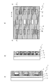
- FIG. 1 is a plan view schematically showing an embodiment of a micro LED display according to the present invention. It is explanatory drawing which shows the micro LED mounting structure by this invention. It is explanatory drawing which shows an example of a cell. It is a detailed explanatory view of the cell shown in FIG. 3 is a flowchart showing steps of a method for manufacturing a micro LED display according to the present invention. It is explanatory drawing which shows an example of a wafer. It is a flowchart which shows the process of processing a wafer. It is explanatory drawing which shows the state by which the 1st adhesive agent was laminated
- FIG. 6 is a process diagram illustrating a process from alignment to bonding shown in FIG. 5.
- FIG. 6 is a process diagram illustrating a process from pressing to separation of a wafer shown in FIG. 5. It is a graph which shows the temperature characteristic of the viscosity of a 1st adhesive agent and a 2nd adhesive agent.
- FIG. 1 is a plan view schematically showing an embodiment of a micro LED display according to the present invention.
- This micro LED display is a device capable of full color display by combining a micro LED and an RGB phosphor, and includes an LED array substrate 1 and a fluorescent light emitting layer array 2.
- the micro LED display according to the present invention can be applied to a flat display or a flexible display. When this micro LED display is applied to, for example, a flat display, illustration of a protective glass as another component is omitted in FIG. 1.
- the LED array substrate 1 is for individually emitting micro LEDs 3 (hereinafter, simply referred to as “LED3”), and includes a plurality of LEDs 3 arranged in a matrix as shown in FIG. 1 and a wiring substrate for driving the LEDs 3. Including 4 and.
- the fluorescent light emitting layer array 2 is excited by the light (excitation light) emitted from the LED 3 and wavelength-converted into fluorescence of corresponding colors of R (red), G (green) and B (blue) which are the three primary colors of light. And a plurality of fluorescent light emitting layers containing the fluorescent material.
- the fluorescent light emitting layer array 2 has a plurality of fluorescent light emitting layers 11 arranged in a matrix.
- a combination of three LEDs 3 corresponding to one pixel and one fluorescent light emitting layer 11 including the fluorescent material layers 11R, 11G, and 11B provided on each LED 3 is one cell. 21. That is, by combining the LED array substrate 1 and the fluorescent light emitting layer array 2, the cells 21 can be handled as a unit. As a result, in the micro LED display, the plurality of cells 21 for realizing full-color display are arranged in a matrix. In FIG. 1, the cells 21 are arranged in 4 rows and 5 columns for easy understanding of the description.
- the fluorescent light emitting layer 11 has a fluorescent material layer 11R filled with a red fluorescent dye, a fluorescent material layer 11G filled with a green fluorescent dye, and a fluorescent material layer 11B filled with a blue fluorescent dye. These fluorescent dyes are examples of RGB phosphors.
- the LED 3 emits light having a specific spectrum and is manufactured using gallium nitride (GaN) as a main material.
- the LED 3 is an ultraviolet light emitting diode (UV-LED), and is an LED that emits near-ultraviolet light having a wavelength of, for example, 200 nm to 380 nm.
- the LED 3 may be an LED that emits blue light having a wavelength of, for example, 380 nm to 500 nm.
- Near-ultraviolet light having a wavelength of, for example, 200 nm to 380 nm and blue light having a wavelength of, for example, 380 nm to 500 nm correspond to an example of light having a specific spectrum.
- FIG. 2 is an explanatory view showing a micro LED mounting structure according to the present invention.
- the LED array substrate 1 is an example of a micro LED mounting structure according to the present invention.
- FIG. 2A shows a sectional view taken along the line AA of the LED array substrate 1 in the region surrounded by the broken line R1 shown in FIG. 2B is a sectional view taken along line BB of the LED array substrate 1 in the area surrounded by the broken line R1 shown in FIG. 2C is an enlarged view of a main part of the LED array substrate 1 surrounded by a broken line R2 shown in FIG. 2A, and FIG. 2D is a broken line R3 shown in FIG. 2B. It is a principal part enlarged view of the LED array substrate 1 enclosed.
- the LED array substrate 1 has a wiring substrate 4 on a base substrate 5, the LEDs 3 are connected on the wiring substrate 4, and a flattening film 9 is further laminated. It has a structure. Then, the wiring board 4 and the LED 3 are excellently realized by a first adhesive 6 and a second adhesive 8, which will be described later, in a mechanical connection and an electrical connection.
- the LED 3 has a compound semiconductor 30 including a plurality of layers such as a peeling layer for laser lift-off and a light emitting layer.
- the LED 3 has LED electrodes 31a and 31b for light emission at a predetermined position on one surface of the compound semiconductor 30, and a light emitting surface 32 for emitting light from a light source (light emitting layer) on the other surface. Are formed.
- Laser lift-off is, for example, a means of irradiating an LED formed on one surface of a sapphire substrate with laser light by pulse oscillation from the other surface of the sapphire substrate to separate each LED from the sapphire substrate.
- a laser beam by focusing and irradiating a laser beam on an interface region (for example, a peeling layer) at a portion to be peeled off, for example, due to a phenomenon that nitrogen of GaN is vaporized, an LED is emitted in the interface region. It is separated from the sapphire substrate.
- a YAG laser oscillator in the solid-state UV (Ultra Violet) region uses a fourth harmonic (FHG: Fourth-Harmonic Generation) wavelength of 266 nm. It is preferable to use a picosecond pulsed laser.
- the wafer 10 which is a transparent substrate such as sapphire is adjusted by adjusting parameters such as laser power, a laser beam irradiation region, and the number of times of irradiation based on pulse irradiation using a device for performing laser lift-off. (See FIG. 6) is not peeled from the LED 3, but the wafer 10 is easily peeled from the LED 3. Details will be described later with reference to FIGS. 9 to 11.
- the wiring board 4 is, for example, a flexible printed wiring board (FPC: Flexible Printed Circuits), and is a film-like board including an insulating base film (for example, polyimide) and a wiring layer on which an electric circuit is formed. is there.
- the wiring board 4 has bump electrodes 7 for conductive connection arranged on one surface in accordance with a predetermined arrangement. Wiring is provided on the wiring board 4 so that a driving circuit (not shown) provided outside can supply a driving current for turning on and off to each of the plurality of LEDs 3.
- the base substrate 5 supports the wiring substrate 4 on which the LEDs 3 are mounted, and is a transparent substrate such as quartz glass.
- the first adhesive 6 ensures adhesion and conduction between the LED electrodes 31a and 31b and the bump electrodes 7.
- the first adhesive 6 is a resin composition that is laminated on the LED electrode surface of each LED 3 and includes a thermosetting adhesive having conductivity and the like.
- the bump electrode 7 is an example of an electrode portion, is provided on the wiring board 4, and is electrically connected to the LED electrodes 31a and 31b (see FIG. 2D) of the LED 3 via the first adhesive 6. It is a possible electrode.
- the bump electrode 7 has, for example, conductivity and is elastically deformed by applying pressure. As a result, the connection between the LED electrodes 31a and 31b of the LED 3 and the wiring board 4 becomes more reliable.
- the second adhesive 8 is provided on the wiring board 4 and is adhered so as to surround part or all of the peripheral side surface of the LED 3 including the LED electrodes 31a and 31b in which the first adhesive 6 is laminated.
- the flattening film 9 is a film that is laminated in a region including the light emitting surface 32 of the LED 3 and has a flat plate shape.
- the thickness of the flattening film 9 is determined on the light emitting surface 32 based on the emission angle of the light emitted from the light emitting surface 32. Details will be described later with reference to FIGS.
- each LED 3 is pressed against the bump electrode 7 via the first adhesive 6, and the first bonding is performed.
- the agent 6 and the second adhesive 8 are cured by heating.
- the LED electrodes 31a and 31b of the LED 3 and the bump electrodes 7 of the wiring board 4 are bonded together via the first adhesive 6. Specifically, as described later, the LED electrode 31a and the bump electrode 7 (anode electrode 7a shown in FIG. 13) are adhered to each other via the first adhesive 6. Further, the LED electrode 31b and the bump electrode 7 (cathode electrode 7b shown in FIG. 13) are adhered to each other via the first adhesive 6. Further, a part of the peripheral side surface of the LED 3 is surrounded and adhered by the second adhesive agent 8, and each LED 3 is fixed to the wiring board 4 via the second adhesive agent 8. The entire peripheral side surface of the LED 3 may be surrounded and adhered by the second adhesive 8.
- FIG. 3 is an explanatory diagram showing an example of a cell.
- FIG. 4 is a detailed explanatory diagram of the cell shown in FIG. 3A is a plan view of the cell 21 shown in FIG. 1, and FIG. 3B is a sectional view taken along the line CC shown in FIG. 3A.
- the cell 21 does not include the wiring substrate 4 and the base substrate 5.
- the fluorescent light emitting layer 11 uses red light (R) for realizing full-color display of red, green, and blue fluorescent dyes (an example of a fluorescent material) by light (excitation light) emitted from the light emitting surface 32 of the LED 3. The wavelengths are converted into green (G) and blue (B) fluorescence, respectively.
- the fluorescent light emitting layer 11 causes the fluorescent dyes of the respective fluorescent material layers 11R, 11G, and 11B to transition to an excited state by excitation light, and then, when the fluorescent dyes return to the ground state, the respective fluorescent materials convert wavelengths.
- the emitted red (R), green (G), and blue (B) corresponding to the visible spectrum emits fluorescence.
- These fluorescent material layers 11R, 11G, and 11B are partitioned by partition walls 12 having a reflective film 13 on the surface.
- the fluorescent light emitting layer 11 is provided on the LED array substrate 1.
- the fluorescent material layer 11R of the fluorescent light emitting layer 11 is formed by mixing and dispersing a fluorescent dye 14a having a particle size of micron size and a fluorescent dye 14b having a particle size of nanosize in a resist film.
- the fluorescent material layer 11G is formed by mixing and dispersing a fluorescent dye 14c having a micron-sized particle diameter and a fluorescent pigment 14d having a nano-sized particle diameter, like the fluorescent material layer 11R.
- the fluorescent material layer 11B is formed by mixing and dispersing a fluorescent dye 14e having a particle size of micron size and a fluorescent dye 14f having a particle size of nano size.
- a fluorescent dye 14e having a particle size of micron size and a fluorescent dye 14f having a particle size of nano size.
- the fluorescent dyes with nano-sized particles can prevent the leakage of excitation light due to the decrease in the packing ratio of the fluorescent dyes, and the fluorescent dyes with micron-sized particles can be used. Can improve the luminous efficiency.
- the partition wall 12 is an example of a light shielding wall, and separates the fluorescent material layers 11R, 11G, and 11B from each other.
- the partition wall 12 is formed of, for example, a transparent photosensitive resin.
- the partition wall 12 in order to increase the filling rate of the fluorescent dye 14a having a particle size larger than that of the fluorescent dye 14b, the partition wall 12 has an aspect ratio of height to width of 3 or more. It is desirable to use high aspect materials that allow. The same applies to the fluorescent material layers 11G and 11B.
- An example of such a high aspect material is SU-83000 photoresist manufactured by Nippon Kayaku Co., Ltd.
- a reflective film 13 is provided on the surface of the partition wall 12, as shown in FIG.
- the reflective film 13 prevents the excitation light and the fluorescent light FL from passing through the partition wall 12 and entering into another adjacent fluorescent material layer.
- This fluorescent light FL emits light when each fluorescent dye of each fluorescent material layer 11R, 11G, and 11B is excited by excitation light.
- the reflective film 13 is formed with a thickness that can sufficiently block the excitation light and the fluorescent light FL.
- the reflection film 13 is preferably a thin film of aluminum or aluminum alloy that easily reflects the excitation light and the fluorescent light FL.
- the fluorescent light emitting layer 11 can be used to emit light from the fluorescent material layers 11R, 11G, and 11B by reflecting the excitation light toward the partition wall 12 with the reflective film 13 such as aluminum. Therefore, the luminous efficiency of each of the fluorescent material layers 11R, 11G, and 11B is improved.
- the thin film deposited on the surface of the partition wall 12 is not limited to the reflective film 13 that reflects the excitation light and the fluorescence FL, and may be one that absorbs the excitation light and the fluorescence FL.
- the configuration of the micro LED display of the present invention has been described above.
- the LED electrodes 31a and 31b of each LED 3 and the bump electrode 7 are connected via the first adhesive 6 having conductivity, and the bumps 7 are attached to the peripheral side surface of the LED 3.
- a part of the LED 3 is surrounded and adhered by a second adhesive having an insulating property, and the LED 3 is fixed to the wiring board 4 via the second adhesive.
- the LED electrodes 31a and 31b of the LED 3 and the bump electrodes 7 of the wiring board 4 can be reliably bonded and conducted, and the LED 3 is bonded via the second adhesive.
- the wiring board 4 can be securely fixed and connected. That is, in the micro LED mounting structure according to the present invention, the electrical and mechanical connection between the LED 3 and the wiring board 4 can be reliably performed.
- the micro LED display of the present invention since the LED array substrate 1 is provided as the micro LED mounting structure, it is possible to surely perform the electrical and mechanical connection between the LED 3 and the wiring substrate 4. Then, by supplying a drive current to the wiring board 4 from a drive circuit provided outside, the micro LED display of the present invention can perform full color display.
- FIG. 5 is a flowchart showing steps of the method for manufacturing a micro LED display according to the present invention.
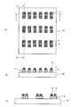
- FIG. 6 is an explanatory diagram showing an example of a wafer.
- FIG. 3A is a plan view of the wafer 10.
- (B) is a DD line sectional view of (a)
- (c) is a EE line sectional view of (a).
- a wafer 10 having a plurality of LEDs 3 arranged in a matrix (3 rows and 6 columns) at a predetermined interval on one surface (front surface) is used to A method for manufacturing the LED display will be described.
- the plurality of LEDs 3 are formed on one surface of the wafer 10 by a crystal growth process such as MOCVD (Metal Organic Chemical Vapor Deposition).
- MOCVD Metal Organic Chemical Vapor Deposition
- the LEDs 3 are arranged, for example, with a pitch of W 1 in the column direction (y direction) and with a pitch of W 2 in the row direction (x direction). ..
- the ratio P 1 (W 2 /W 1 ) between W 1 and W 2 is preferably about 3 in the arrangement shown in FIG. Therefore, for example, the pitch of W 1 is 50 ⁇ m and the pitch of W 2 is 150 ⁇ m.
- the height (h 1 ) for example, a size of several ⁇ m to 30 ⁇ m can be targeted.
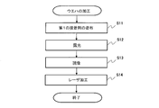
- FIG. 7 is a flowchart showing the steps of wafer processing.
- the processes from step S11 to step S14 shown in FIG. 7 are performed.
- a photolithography technique using a photomask (not shown) is applied to apply the thermosetting first adhesive 6 having conductivity and photosensitivity to the wafer 10. Apply.
- the first adhesive 6 is laminated on the LED electrodes 31a and 31b by patterning by exposure and development. The details will be described below.
- the first adhesive 6 is applied on the surface of the wafer 10 on which the LEDs 3 are arranged.
- the first adhesive 6 is, for example, a resin composition in which an electrically conductive material, an adhesive material, and a photosensitizer are mixed with an insulating thermosetting resin.
- the first adhesive 6 is a resin composition that develops an adhesive function and is cured by heating.
- the adhesive material may be, for example, a thermosetting epoxy resin.
- the first adhesive 6 contains, as a conductive material, for example, fine carbon particles selected from a particle diameter in the range of 10 nm to 1.0 ⁇ m, and has a conductive function added. .. In the present embodiment, as an example, fine particles of carbon of about 0.5 ⁇ m to 1.0 ⁇ m are used.
- the first adhesive 6 contains a photosensitizer, it has a photosensitivity function capable of patterning by ultraviolet rays. That is, the first adhesive 6 also functions as a photoresist.
- the first adhesive 6 may be a resin composition in which a conductive material and a photosensitizer are mixed, and the adhesive strength is further increased. Adhesive materials may be included to enhance.
- the conductive material is not limited to the above-mentioned carbon, and metal fine particles may be adopted.
- the fine metal particles are preferably silver (Ag), for example.
- nickel (Ni), copper (Cu), aluminum (Al), gold (Au) or the like may be adopted depending on the application.
- an applicable material may be selected from metal nanoparticles having a metal particle diameter of about 10 nm to metal fine particles having a particle diameter of 1.0 ⁇ m or less.
- step S11 the first adhesive 6 is applied onto the surface of the wafer 10 on which the LEDs 3 are arranged, for example, using a spin coater (not shown) used in photolithography technology.
- the spin coater is a device for realizing uniform coating.
- the first adhesive 6 is dropped onto the wafer 10 as a photoresist, and the wafer 10 is set on the surface of the wafer 10 by setting a predetermined rotation speed and rotation time.
- Adhesive 6 of No. 1 is applied.
- a bar coater may be applied as a means for applying a uniform film thickness.
- the wafer 10 coated with the first adhesive 6 is pre-baked by a heating means such as a heater (not shown).
- the prebaking conditions are, for example, a heating temperature of 100° C. and a heating time of 1 minute.
- step S12 the wafer 10 coated with the first adhesive 6 is irradiated with ultraviolet (UV) light through a photomask.
- step S13 the wafer 10 is immersed in a developing solution for cleaning. As a result, the first adhesive 6 is laminated on the LED electrodes 31a and 31b.
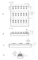
- FIG. 8 is an explanatory diagram showing a state in which the first adhesive is laminated on the LED electrodes.
- FIG. 3A is a plan view of the surface of the wafer 10.
- (B) is the FF line sectional view of (a)
- (c) is the GG line sectional view of (a).
- the film thickness (h 2 ) of the first adhesive 6 laminated on the LED electrodes 31a and 31b is, for example, 2 ⁇ m.
- the interface between the wafer 10 and the LED 3 is focused and irradiated with the laser light L from the back surface of the wafer 10.
- the laser beam L is irradiated from the back surface of the wafer 10 to weaken the bonding state of the LEDs 3 formed on the front surface of the wafer 10 as compared with that before the laser beam L is irradiated.
- Perform processing In this case, in step S14, the laser lift-off for peeling the LED 3 from the wafer 10 is not performed, but the LED 3 is easily peeled off.
- the state of easy peeling means a state in which the adhesive force of the second adhesive 8 bonded to the LED 3 is larger than the adhesive force of the LED 3 bonded to the wafer 10 in the bonded state.
- FIG. 9 to 11 are explanatory views of laser processing.
- (a) is a plan view of the wafer 10 seen from the back surface.
- the wafer 10 is transparent, the light emitting surface 32 of the LED 3 is visible.
- (a) schematically illustrates a state in which the laser light L is focused and applied to the boundary between the light emitting surface 32 of one LED 3 and the wafer 10.
- 9B is a sectional view taken along the line HH of FIG. 9A
- FIG. 9C is a sectional view taken along the line II of FIG. 9A, showing a laser irradiation state.
- the laser processing energy is, for example, weaker than the energy when the LED 3 is laser lifted off, and is preferably processed by a plurality of shots so that the LED 3 is easily peeled off from the wafer 10.
- step S14 for example, about 20 shots may be irradiated with an energy that is 1/2 of that at the time of laser lift-off.
- the peeling layer in the LED 3 is modified so that the wafer 10 can be peeled from the wiring substrate 4 without laser irradiation in the wafer peeling (step S8) described below.
- the modified release layer is referred to as a GaN re-fusion layer.
- the adhesive force of the GaN re-fusion layer to the wafer 10 is the adhesive force in the bonded state of the LED 3, and may be, for example, 230 kg/cm 2 or less.
- the adhesive force of the GaN re-fusion layer is preferably about 100 kg/cm 2 .
- step S14 as shown in FIG. 10, the light emitting surface 32 of one LED 3 is divided into two parts such as the upper half surface and the lower half surface of the light emitting surface 32 by using a projection mask or a slit.
- the laser light L may be emitted.
- FIG. 10 shows a state in which the LEDs 3 are sequentially irradiated with the laser light L by moving the wafer 10 in steps.
- each LED 3 is irradiated with the laser light L divided by a projection mask or the like so that the entire surface of the light emitting surface 32 is not irradiated with the laser light L at a time.
- FIG. 11 shows a state in which the LEDs 3 are sequentially irradiated with the laser light L by moving the wafer 10 in steps. As described above, the wafer processing (step S1) is completed, and the process proceeds to the wiring board processing (step S2).
- FIG. 12 is a flowchart showing the steps of processing the wiring board.
- step S2 the processing from step S21 to step S24 shown in FIG. 12 is performed.
- FIG. 13 is an explanatory diagram showing an example of a wiring board on which bump electrodes are formed.
- FIG. 7A is a plan view of the wiring board 4 on which the bump electrodes 7 are formed.
- B is a sectional view taken along the line JJ of (a)
- (c) is a sectional view taken along the line KK of (a).
- D) is an enlarged view of a region R5 indicated by a broken line in (b).
- the wiring board 4 is provided with a plurality of electrode pads 4a (see FIG. 13D) corresponding to the LED electrodes 31a and 31b of the plurality of LEDs 3 arranged in a matrix.
- the conductive elastic protrusion 71 is formed on the electrode pad 4a (see FIG. 13D). Specifically, in step S21, a resist for a photo spacer is applied to the entire surface of the wiring board 4, and then exposed by using a photo mask and developed to pattern and form a protrusion on the electrode pad 4a. In step S21, a conductive film 72 of good conductivity such as gold or aluminum is formed on the projection and the electrode pad 4a by sputtering, vapor deposition or the like to form a conductive elastic projection 71.
- the bump electrode 7 including the elastic protrusion 71, the conductor film 72, and the electrode pad 4a is formed.
- the bump electrode 7 is specifically composed of an anode electrode 7a and a cathode electrode 7b corresponding to the LED electrodes 31a and 31b (see FIGS. 13A and 13C).
- the bump electrode 7 has, for example, a height (h 3 ) of 4 ⁇ m and a diameter (d) of 10 ⁇ m (see FIG. 13D).
- the elastic protrusion 71 may be a protrusion formed of a conductive photoresist in which conductive fine particles such as silver are added to the photoresist or a conductive photoresist containing a conductive polymer.
- a conductive photoresist is applied to the entire upper surface of the wiring substrate 4 with a predetermined thickness, and then exposed using a photomask and developed to form protrusions on the electrode pads as elastic protrusions. 71 is patterned.
- the bump electrode 7 is composed of the elastic protrusion 71 having conductivity and the electrode pad 4a. As described above, since the bump electrode 7 can be formed by applying the photolithography process, it is possible to secure high accuracy in position and shape.
- the second adhesive 8 is applied on the wiring board 4 on which the bump electrodes 7 are formed.
- the second adhesive 8 is, for example, a resin composition in which an insulating thermosetting resin is mixed with an adhesive material and a photosensitizer.
- the second adhesive 8 is a resin composition that develops an adhesive function and is cured by heating.
- the second adhesive 8 contains a photosensitizer, it has a photosensitivity function capable of patterning by ultraviolet rays. That is, the second adhesive 8 also functions as a photoresist.
- step S22 the second adhesive 8 is applied onto the wiring board 4 using a spin coater in the same manner as the application of the first adhesive (step S11).
- step S22 the wiring board 4 coated with the second adhesive 8 is pre-baked by a heating means such as a heater (not shown).
- the prebaking conditions are, for example, a heating temperature of 100° C. and a heating time of 5 minutes.
- step S23 the wiring board 4 coated with the second adhesive 8 is irradiated with ultraviolet (UV) light through a photomask.
- step S24 the wiring board 4 is immersed in a developing solution and washed.
- the second adhesive 8 is patterned around each bump electrode 7 (anode electrode 7a and cathode electrode 7b) in a predetermined arrangement by a photomask.
- FIG. 14 is an explanatory diagram showing a state in which the second adhesive is laminated on the wiring board.
- FIG. 3A is a plan view of the surface of the wiring board 4.
- (B) is a sectional view taken along line LL in (a)
- (c) is a sectional view taken along line MM in (a).
- FIG. 15 is an explanatory diagram showing the positional relationship between the second adhesive and the bump electrodes.
- FIG. 14A is an enlarged view of a main part (a portion marked with a reference numeral) of a region R6 indicated by a broken line in FIG.
- FIG. 14B is an enlarged view of the region R7 indicated by the broken line in FIG. (C) is a modification of (b).
- the second adhesive 8 surrounds the bump electrode 7 with a space. Further, as shown in FIG. 15A, the height (h 4 ) of the second adhesive 8 is set higher than the height (h 3 ) of the bump electrode 7. Height of the second adhesive 8 (h 4) the height of the bump electrode 7 (h 3) the ratio of P 2 (h 4 / h 3 ) , for example, preferably about 1.5. Therefore, in FIG. 15A, the height (h 3 ) of the bump electrode 7 is 4 ⁇ m and the height (h 4 ) of the second adhesive 8 is 6 ⁇ m, as an example.
- the bump electrode 7 is pressed, the first adhesive 6 is also deformed by the pressure so as to fill the gap in the space. By doing so, the bump electrode 7 (anode electrode 7a and cathode electrode 7b) is surely bonded with the first adhesive 6 before thermosetting.
- the second adhesive 8 leaves a space and surrounds the periphery of the bump electrode 7, it is not limited to the space having the shape as shown in FIG. 15B, but the shape as shown in FIG. 15C. It may be a space.
- the order of execution of the wafer processing (step S1) and the wiring board processing (step S2) shown in FIG. 5 may be interchanged.
- step S3 when the surface of the wafer 10 and the surface of the wiring substrate 4 are bonded together, a mechanism (not shown) capable of alignment is provided on the wafer 10 and the wiring substrate 4 in advance. Using the provided alignment marks (not shown). Align.
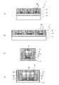
- FIG. 16 is a process diagram illustrating the process from the alignment to the bonding shown in FIG.
- FIG. 17 is a process diagram for explaining the process from pressing to peeling of the wafer shown in FIG.
- FIG. 16A is a diagram showing the alignment between the wafer 10 and the wiring board 4.
- step S3 the LED electrode 31a and the anode electrode 7a of the wiring substrate 4 are aligned so as to contact each other via the first adhesive 6, and the LED electrode 31b and the wiring are connected via the first adhesive 6.
- the substrate 4 is aligned so as to come into contact with the cathode electrode 7b.
- FIG. 16B illustrates a state where the first adhesive 6 and the second adhesive 8 are heated by the heater H.
- FIG. 18 is a graph showing the temperature characteristics of the viscosities of the first adhesive and the second adhesive.
- FIG. 18 shows the outline of the experimental results.
- the horizontal axis represents temperature (° C.), and the vertical axis represents arbitrary unit of viscosity (Pa).
- the first adhesive 6 and the second adhesive 8 used in this embodiment have the characteristic that the viscosity becomes the lowest at about 120°C.
- the first adhesive 6 and the second adhesive 8 may be adhesives having both thermoplasticity and thermosetting, 120° C. and It has the characteristic that it becomes the softest before and after.
- it is preferable that the first adhesive 6 and the second adhesive 8 are attached in the softest state and pressed. Therefore, the first adhesive 6 and the second adhesive 8 are heated to about 120° C., and the process proceeds to bonding (step S5).
- step S5 the wafer 10 and the wiring board 4 are bonded together based on the alignment mark described above.
- FIG. 16C is a diagram showing the bonding between the wafer 10 and the wiring board 4.
- the wafer 10 is lowered by an elevating mechanism (not shown) while the first adhesive 6 and the second adhesive 8 are heated to about 120° C., and the wiring substrate 4 and the wafer 10 are bonded to each other.
- the first adhesive 6 on one side and the anode electrode 7a of the wiring board 4 contact each other, and the first adhesive 6 on the other side and the cathode electrode 7b of the wiring board 4 contact each other. The state which abutted is illustrated.
- step S6 the wafer 10 is further lowered by the elevating mechanism to press the wafer 10 against the wiring substrate 4 at a predetermined pressure P.
- the LED electrodes 31a and 31b of the LEDs 3 on the wafer 10 and the bump electrodes 7 on the wiring board 4 are bonded together via the first adhesive 6 and pressed.
- FIG. 17A is a diagram showing a state in which the wafer 10 is pressed against the wiring board 4 with the pressure P.
- step S7 the first adhesive 6 and the second adhesive 8 are heated by the heater H in order to be further hardened.
- step S7 for example, the curing temperature is set to 230° C. and the heating time is set to 30 minutes to cure the first adhesive agent 6 and the second adhesive agent 8.
- the curing temperature may be set to 200° C. and the heating time may be set to 60 minutes.
- the curing temperature may be 180° C. and the heating time may be 90 minutes.
- FIG. 17B illustrates a state in which the first adhesive 6 and the second adhesive 8 are further heated using the heater H.
- step S8 the bonded wafer 10 and the wiring board 4 are cooled and returned to room temperature (for example, 25° C.), and then the wafer 10 is lifted by the elevating mechanism to move the wafer 10 to the wiring board 4 Peel from. As a result, the LED 3 is mounted on the wiring board 4.
- room temperature for example, 25° C.
- FIG. 19 is an explanatory diagram of the LED array substrate formed by peeling the wafer.
- FIG. 3A is a plan view of the LED array substrate 1.
- (B) is a sectional view taken along line NN of (a), and
- (c) is a sectional view taken along line OO of (a).
- the LED array substrate 1 is an example of a micro LED mounting structure as described above.
- step S9 for example, a transparent insulating photosensitive resin is applied onto the LED array substrate 1 shown in FIG. 19 by using a micro dispenser (not shown) under automatic control. Then, the flattening film 9 is formed by irradiating the photosensitive resin with ultraviolet (UV) light to cure it. That is, the flattening film 9 is laminated on the LED array substrate 1. In this case, all the LEDs 3 are covered with the flattening film 9. In this embodiment, since the photosensitive resin is applied so as to have a uniform height, the flattened film 9 having a flat plate shape is formed.
- UV ultraviolet
- FIG. 20 is an explanatory diagram of an LED array substrate on which a flattening film is laminated.
- FIG. 3A is a plan view of the LED array substrate 1 on which a flattening film is formed.
- (B) is a sectional view taken along the line PP of (a), and
- (c) is a sectional view taken along the line QQ of (a).
- 20A since the flattening film 9 is transparent, the light emitting surface 32 of each LED 3 can be seen.
- the flattening film 9 will be described later with reference to FIG.
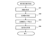
- FIG. 21 is a flowchart showing the steps of forming the fluorescent light emitting layer.
- FIG. 22 is a process diagram illustrating a process of forming a fluorescent light emitting layer. In the formation of the fluorescent light emitting layer (step S10), the processes from step S31 to step S34 shown in FIG. 22 are performed.
- step S31 the partition 12 is formed on the LED array substrate 1 on which the flattening film 9 is formed.
- FIG. 22A shows a state in which the partition wall 12 is provided on the LED array substrate 1 shown in FIG. 20B.
- step S31 for example, a transparent photosensitive resin for the partition wall 12 is applied, and then exposed using a photomask and developed to form the respective fluorescent material layers 11R, 11G, and 11B (see FIG. 22D).
- the opening 12a is provided in accordance with the above (see).
- the transparent partition wall 12 having a height-to-width aspect ratio of 3 or more is formed with a height of about 20 ⁇ m per minute.
- the photosensitive resin used is preferably a high aspect material such as SU-83000 manufactured by Nippon Kayaku Co., Ltd., for example.
- a film formation technique such as sputtering is applied from the side of the partition 12 formed on the LED array substrate 1 to form a predetermined reflection film 13 such as aluminum or aluminum alloy.
- the film is formed to a thickness.
- the reflection film 13 may be formed to have a predetermined thickness by plating.
- FIG. 22B shows a state after the reflective film 13 is formed.
- the unnecessary reflection film 13 is removed.
- the reflection film 13 covering the upper portion of the opening surrounded by the partition 12 is removed by laser irradiation suitable for laser processing of the reflection film 13.
- the laser irradiation removes the reflection film 13 in the region other than the side surface inside the opening.
- the second harmonic SHG: Second-Harmonic Generation
- the third harmonic TMG: Third-Harmonic Generation
- the fourth harmonic has a wavelength of 266 nm.
- FIG. 22C shows a state where the reflective film 13 is formed on the partition wall 12 after laser processing.
- step S34 in the filling of the fluorescent material (step S34), as the fluorescent material of RGB, a red fluorescent pigment is filled in the opening corresponding to red to form the fluorescent material layer 11R, and a green fluorescent pigment is filled in the opening corresponding to green.
- a fluorescent material layer 11G blue fluorescent dye is filled in the opening corresponding to blue to form the fluorescent material layer 11B.
- step S34 a resist containing the red fluorescent dye 14 is applied, and then exposed by using a photomask, developed, and baked, whereby the red fluorescent material is provided in the opening corresponding to red.
- the layer 11R is formed.
- the resist is obtained by mixing and dispersing the fluorescent dye 14a having a large particle diameter and the fluorescent dye 14b having a small particle diameter.
- step S34 the method of forming the red fluorescent material layer 11R in the opening corresponding to red is similarly applied to form the green fluorescent material layer 11G in the opening corresponding to green. Further, in step S34, the technique of forming the red fluorescent material layer 11R in the opening corresponding to red is similarly applied to form the blue fluorescent material layer 11B in the opening corresponding to blue.
- FIG. 22D is a diagram showing a state after filling the RGB fluorescent materials.
- the fluorescent light emitting layer 11 can be formed on the LED array substrate 1 as shown in FIG.
- FIG. 23 is an explanatory diagram showing the influence of the thickness of the flattening film on the light emission.
- the thickness (T) of the flattening film 9 indicates the distance from the bottom surface of the partition wall 12 to the light emitting surface 32 of the LED 3.
- the flattening film 9 may not have the thickness (T), or may have a predetermined thickness (see FIG. 23A).
- FIG. 23A shows a state in which the partition wall 12 is formed in the sectional view taken along the line PP of FIG. 20A.
- the thickness (T) is made larger than that in FIG. 23(a). That is, depending on the thickness (T) of the flattening film 9, light emitted from the light emitting surface 32 of the LED 3 may enter the adjacent fluorescent material layer. In this case, for example, when the light emission of the LED 3 located immediately below the adjacent fluorescent material layer is turned off (extinguished), the adjacent fluorescent material layer may also emit fluorescent light FL to cause color mixing (see FIG. 23(b)). ). Therefore, it is desirable that the thickness (T) of the flattening film 9 be optimized.
- FIG. 23C is an explanatory diagram for optimizing the thickness (T) of the flattening film.
- the thickness (T) of the flattening film 9 is obtained depending on parameters including the width D1 of the partition wall 12, the lateral width D2 of the LED 3, and the emission angle ( ⁇ ) of the light emitted from the light emitting surface 32 of the LED 3.
- the emission angle ( ⁇ ) of the light emitted from the light emitting surface 32 intersects with the horizontal line of the light emitting surface 32 and the vector of the arrow A indicating the light emitting direction in the cross-sectional view of FIG. Angle. That is, in the flattening film 9, the thickness (T) on the light emitting surface 32 is determined based on the light emission angle ( ⁇ ).
- the thickness (T) of the flattening film 9 is based on the parameters including the width D1 of the partition wall 12, the lateral width D2 of the LED 3, and the emission angle ( ⁇ ) of the light emitted from the light emitting surface 32 of the LED 3.
- the manufacturing method of the micro LED display of the present invention it is possible to manufacture the micro LED display including the micro LED mounting structure of the present invention as described above. As a result, it is possible to improve the yield due to a defective connection of the micro LED in the manufacturing stage of the micro LED display.
- the bump-free electrode wiring may be provided as the electrode portion on the surface of the wiring board 4.
- the bonding surface is small, so that soldering or anisotropic conductive film (ACF: Anisotropic Conductive Film) is used. ) Was difficult to bond.
- ACF Anisotropic Conductive Film
- the above embodiment is characterized in that the electrode surfaces are adhered to each other and the side surfaces of the LED 3 are adhered to each other, and a stable connection and a strong adhesive force can be obtained even for a minute micro LED like the LED 3.
- LED array substrate (micro LED mounting structure) 2... Fluorescent light emitting layer array 3... Micro LED 4... Wiring board 6... 1st adhesive agent 7... Bump electrode 8... 2nd adhesive agent 9... Flattening film 11... Fluorescent light emitting layer 21... Cell 31a, 31b... LED electrode 32... Light emission surface
Landscapes
- Led Device Packages (AREA)
- Devices For Indicating Variable Information By Combining Individual Elements (AREA)
Abstract
La présente invention concerne une structure de montage de micro-LED comprenant : une carte de câblage (4) qui comporte, sur l'un de ses côtés, des parties d'électrode (7) agencées selon un réseau prédéterminé ; et une micro-LED (3) qui est disposée de façon à correspondre aux positions des parties d'électrode (7), qui émet de la lumière présentant un spectre déterminé allant de la bande des longueurs d'ondes ultraviolettes à la bande des longueurs d'ondes bleues, qui comporte, sur l'une de ses surfaces parmi ses surfaces se faisant face, des électrodes (31a, 31b) qui sont électriquement connectées aux parties d'électrode (7), et qui comporte, sur son autre surface, une surface d'émission de lumière (32) qui projette la lumière émise. Les électrodes (31a, 31b) et les parties d'électrode (7) sont liées par un premier adhésif (6) thermodurcissable conducteur. Tout ou partie de la surface latérale périphérique de la micro-LED (3) est renfermée et liée par un second adhésif (8) thermodurcissable isolant. La micro-LED (3) est fixée à la carte de câblage par l'intermédiaire du second adhésif (8). Grâce à cette configuration, l'invention concerne un moyen pour lier et connecter électriquement de façon fiable les électrodes de la micro-LED aux parties d'électrode de la carte de câblage et pour connecter de façon fiable la micro-LED à la carte de câblage.
Applications Claiming Priority (2)
| Application Number | Priority Date | Filing Date | Title |
|---|---|---|---|
| JP2018-227975 | 2018-12-05 | ||
| JP2018227975A JP2020092159A (ja) | 2018-12-05 | 2018-12-05 | マイクロled実装構造、マイクロledディスプレイ及びマイクロledディスプレイの製造方法 |
Publications (1)
| Publication Number | Publication Date |
|---|---|
| WO2020116207A1 true WO2020116207A1 (fr) | 2020-06-11 |
Family
ID=70973740
Family Applications (1)
| Application Number | Title | Priority Date | Filing Date |
|---|---|---|---|
| PCT/JP2019/045816 Ceased WO2020116207A1 (fr) | 2018-12-05 | 2019-11-22 | Structure de montage de micro-led, unité d'affichage à micro-led et procédé de fabrication d'une unité d'affichage à micro-led |
Country Status (3)
| Country | Link |
|---|---|
| JP (1) | JP2020092159A (fr) |
| TW (1) | TW202032817A (fr) |
| WO (1) | WO2020116207A1 (fr) |
Cited By (6)
| Publication number | Priority date | Publication date | Assignee | Title |
|---|---|---|---|---|
| WO2022052310A1 (fr) * | 2020-09-09 | 2022-03-17 | 深圳市奥拓电子股份有限公司 | Procédé, dispositif et système d'affichage à fluorescence excitée par del ultraviolettes |
| JPWO2023182263A1 (fr) * | 2022-03-25 | 2023-09-28 | ||
| CN117083656A (zh) * | 2021-03-26 | 2023-11-17 | 京瓷株式会社 | 显示装置 |
| WO2024204455A1 (fr) * | 2023-03-29 | 2024-10-03 | 東レエンジニアリング株式会社 | Dispositif de transfert d'élément et procédé de transfert d'élément |
| EP4400904A4 (fr) * | 2022-01-19 | 2025-02-19 | Samsung Electronics Co., Ltd. | Écran d'affichage et dispositif d'affichage le comprenant |
| US12288769B2 (en) | 2021-04-30 | 2025-04-29 | Sharp Kabushiki Kaisha | Micro-LED mounting substrate, micro-led display, and method of manufacturing micro-LED mounting substrate |
Families Citing this family (11)
| Publication number | Priority date | Publication date | Assignee | Title |
|---|---|---|---|---|
| CN115769145A (zh) | 2020-08-07 | 2023-03-07 | 东丽株式会社 | 导电糊剂、印刷布线板、印刷布线板的制造方法、印刷电路板的制造方法 |
| TWI796598B (zh) * | 2020-09-22 | 2023-03-21 | 宏齊科技股份有限公司 | 全彩顯示裝置 |
| TWI780503B (zh) * | 2020-10-22 | 2022-10-11 | 欣興電子股份有限公司 | 發光封裝體及其製造方法 |
| TWI757037B (zh) * | 2021-01-06 | 2022-03-01 | 揚朋科技股份有限公司 | 顯示面板的修補方法 |
| KR20220114967A (ko) * | 2021-02-09 | 2022-08-17 | 삼성전자주식회사 | 디스플레이 모듈 및 그 제조 방법 |
| TWI781754B (zh) * | 2021-09-08 | 2022-10-21 | 隆達電子股份有限公司 | 像素單元與其製造方法 |
| JP7772081B2 (ja) * | 2021-11-04 | 2025-11-18 | コニカミノルタ株式会社 | 隔壁形成用インクジェットインク、及びledデバイス |
| KR20240118058A (ko) * | 2021-12-06 | 2024-08-02 | 도레이 카부시키가이샤 | Led 실장 기판의 제조 방법 |
| CN117012863A (zh) * | 2022-04-29 | 2023-11-07 | 深超光电(深圳)有限公司 | 发光装置、发光装置制作方法和发光装置修补方法 |
| JP2024017711A (ja) * | 2022-07-28 | 2024-02-08 | デクセリアルズ株式会社 | 発光装置の製造方法及び黒色転写フィルム |
| WO2024058282A1 (fr) * | 2022-09-14 | 2024-03-21 | 엘지전자 주식회사 | Dispositif d'affichage faisant appel à un élément électroluminescent et son procédé de fabrication |
Citations (3)
| Publication number | Priority date | Publication date | Assignee | Title |
|---|---|---|---|---|
| JP2008027933A (ja) * | 2006-07-18 | 2008-02-07 | Sony Corp | 素子、素子の製造方法、基板、基板の製造方法、実装構造体、実装方法、発光ダイオードディスプレイ、発光ダイオードバックライトおよび電子機器 |
| US20180233536A1 (en) * | 2014-10-17 | 2018-08-16 | Intel Corporation | Microled display & assembly |
| JP2018182282A (ja) * | 2017-04-21 | 2018-11-15 | ルーメンス カンパニー リミテッド | マイクロledディスプレイ装置及びその製造方法 |
-
2018
- 2018-12-05 JP JP2018227975A patent/JP2020092159A/ja active Pending
-
2019
- 2019-11-22 WO PCT/JP2019/045816 patent/WO2020116207A1/fr not_active Ceased
- 2019-11-29 TW TW108143589A patent/TW202032817A/zh unknown
Patent Citations (3)
| Publication number | Priority date | Publication date | Assignee | Title |
|---|---|---|---|---|
| JP2008027933A (ja) * | 2006-07-18 | 2008-02-07 | Sony Corp | 素子、素子の製造方法、基板、基板の製造方法、実装構造体、実装方法、発光ダイオードディスプレイ、発光ダイオードバックライトおよび電子機器 |
| US20180233536A1 (en) * | 2014-10-17 | 2018-08-16 | Intel Corporation | Microled display & assembly |
| JP2018182282A (ja) * | 2017-04-21 | 2018-11-15 | ルーメンス カンパニー リミテッド | マイクロledディスプレイ装置及びその製造方法 |
Cited By (8)
| Publication number | Priority date | Publication date | Assignee | Title |
|---|---|---|---|---|
| WO2022052310A1 (fr) * | 2020-09-09 | 2022-03-17 | 深圳市奥拓电子股份有限公司 | Procédé, dispositif et système d'affichage à fluorescence excitée par del ultraviolettes |
| CN117083656A (zh) * | 2021-03-26 | 2023-11-17 | 京瓷株式会社 | 显示装置 |
| US12288769B2 (en) | 2021-04-30 | 2025-04-29 | Sharp Kabushiki Kaisha | Micro-LED mounting substrate, micro-led display, and method of manufacturing micro-LED mounting substrate |
| EP4400904A4 (fr) * | 2022-01-19 | 2025-02-19 | Samsung Electronics Co., Ltd. | Écran d'affichage et dispositif d'affichage le comprenant |
| JPWO2023182263A1 (fr) * | 2022-03-25 | 2023-09-28 | ||
| WO2023182263A1 (fr) * | 2022-03-25 | 2023-09-28 | 東レ株式会社 | Procédé de production d'un substrat monté sur led comportant un film durci |
| JP7711749B2 (ja) | 2022-03-25 | 2025-07-23 | 東レ株式会社 | 硬化膜付きled実装基板の製造方法 |
| WO2024204455A1 (fr) * | 2023-03-29 | 2024-10-03 | 東レエンジニアリング株式会社 | Dispositif de transfert d'élément et procédé de transfert d'élément |
Also Published As
| Publication number | Publication date |
|---|---|
| JP2020092159A (ja) | 2020-06-11 |
| TW202032817A (zh) | 2020-09-01 |
Similar Documents
| Publication | Publication Date | Title |
|---|---|---|
| WO2020116207A1 (fr) | Structure de montage de micro-led, unité d'affichage à micro-led et procédé de fabrication d'une unité d'affichage à micro-led | |
| TWI745206B (zh) | 發光顯示單元及顯示裝置 | |
| US20200295224A1 (en) | Manufacturing method for led display panel | |
| US20200243739A1 (en) | Board connection structure, board mounting method, and micro-led display | |
| US20200243712A1 (en) | Inspection method for led chip, inspection device therefor, and manufacturing method for led display | |
| JP2020004939A (ja) | 基板実装方法及び電子部品実装基板 | |
| JP2004304161A (ja) | 発光素子、発光装置、画像表示装置、発光素子の製造方法及び画像表示装置の製造方法 | |
| US20200373350A1 (en) | Full-Color Led Display Panel And Method For Manufacturing Same | |
| JP2020043140A (ja) | Led表示パネルの製造方法及びled表示パネル | |
| WO2021010079A1 (fr) | Structure de montage de composant électronique, procédé de montage de composant électronique et panneau d'affichage à del | |
| TW202029531A (zh) | 固晶結構及其製造方法 | |
| US20200411588A1 (en) | Full-Color Led Diplay Panel And Method For Manufacturing Same | |
| JP2020013954A (ja) | 基板接続構造、マイクロledディスプレイ及び部品実装方法 | |
| CN112885823B (zh) | 显示面板及其制备方法、显示装置 | |
| WO2020079921A1 (fr) | Cellule de réparation, dispositif d'affichage à micro-del et procédé de fabrication de la cellule de réparation | |
| JP4749870B2 (ja) | 発光装置の製造方法 | |
| JP7554852B2 (ja) | デバイスおよびそれを製造するための方法 | |
| JP2021056386A (ja) | Led表示装置の製造方法及びled表示装置 | |
| WO2020003869A1 (fr) | Procédé de montage de carte et carte de montage de composants électroniques | |
| JP7573407B2 (ja) | 回路基板の製造方法及び回路基板 | |
| CN113257963A (zh) | 微led芯片结构、制作方法及显示面板 | |
| KR102901591B1 (ko) | 단자가 상부로 형성되는 소자를 포함하는 표시패널 및 이의 제조방법 | |
| JP7769190B2 (ja) | ディスプレイ用基板、ディスプレイ用基板を用いた発光装置及びそれらの製造方法 | |
| TWI703750B (zh) | 顯示面板 | |
| CN112002791B (zh) | Micro-LED芯片及其制作方法、显示面板 |
Legal Events
| Date | Code | Title | Description |
|---|---|---|---|
| 121 | Ep: the epo has been informed by wipo that ep was designated in this application |
Ref document number: 19892218 Country of ref document: EP Kind code of ref document: A1 |
|
| NENP | Non-entry into the national phase |
Ref country code: DE |
|
| 122 | Ep: pct application non-entry in european phase |
Ref document number: 19892218 Country of ref document: EP Kind code of ref document: A1 |