WO2020121856A1 - 光出力システム、測定システム、光学的ポンプ・プローブ走査トンネル顕微鏡システム、演算器、プログラム、演算方法 - Google Patents
光出力システム、測定システム、光学的ポンプ・プローブ走査トンネル顕微鏡システム、演算器、プログラム、演算方法 Download PDFInfo
- Publication number
- WO2020121856A1 WO2020121856A1 PCT/JP2019/046904 JP2019046904W WO2020121856A1 WO 2020121856 A1 WO2020121856 A1 WO 2020121856A1 JP 2019046904 W JP2019046904 W JP 2019046904W WO 2020121856 A1 WO2020121856 A1 WO 2020121856A1
- Authority
- WO
- WIPO (PCT)
- Prior art keywords
- laser
- light
- signal
- timing
- variable delay
- Prior art date
- Legal status (The legal status is an assumption and is not a legal conclusion. Google has not performed a legal analysis and makes no representation as to the accuracy of the status listed.)
- Ceased
Links
Images




Classifications
-
- G—PHYSICS
- G01—MEASURING; TESTING
- G01Q—SCANNING-PROBE TECHNIQUES OR APPARATUS; APPLICATIONS OF SCANNING-PROBE TECHNIQUES, e.g. SCANNING PROBE MICROSCOPY [SPM]
- G01Q60/00—Particular types of SPM [Scanning Probe Microscopy] or microscopes; Essential components thereof
- G01Q60/10—STM [Scanning Tunnelling Microscopy] or apparatus therefor, e.g. STM probes
- G01Q60/12—STS [Scanning Tunnelling Spectroscopy]
-
- G—PHYSICS
- G01—MEASURING; TESTING
- G01N—INVESTIGATING OR ANALYSING MATERIALS BY DETERMINING THEIR CHEMICAL OR PHYSICAL PROPERTIES
- G01N21/00—Investigating or analysing materials by the use of optical means, i.e. using sub-millimetre waves, infrared, visible or ultraviolet light
- G01N21/62—Systems in which the material investigated is excited whereby it emits light or causes a change in wavelength of the incident light
- G01N21/63—Systems in which the material investigated is excited whereby it emits light or causes a change in wavelength of the incident light optically excited
- G01N21/636—Systems in which the material investigated is excited whereby it emits light or causes a change in wavelength of the incident light optically excited using an arrangement of pump beam and probe beam; using the measurement of optical non-linear properties
-
- G—PHYSICS
- G01—MEASURING; TESTING
- G01Q—SCANNING-PROBE TECHNIQUES OR APPARATUS; APPLICATIONS OF SCANNING-PROBE TECHNIQUES, e.g. SCANNING PROBE MICROSCOPY [SPM]
- G01Q30/00—Auxiliary means serving to assist or improve the scanning probe techniques or apparatus, e.g. display or data processing devices
- G01Q30/02—Non-SPM analysing devices, e.g. SEM [Scanning Electron Microscope], spectrometer or optical microscope
- G01Q30/025—Optical microscopes coupled with SPM
-
- G—PHYSICS
- G01—MEASURING; TESTING
- G01N—INVESTIGATING OR ANALYSING MATERIALS BY DETERMINING THEIR CHEMICAL OR PHYSICAL PROPERTIES
- G01N21/00—Investigating or analysing materials by the use of optical means, i.e. using sub-millimetre waves, infrared, visible or ultraviolet light
- G01N21/01—Arrangements or apparatus for facilitating the optical investigation
-
- G—PHYSICS
- G01—MEASURING; TESTING
- G01N—INVESTIGATING OR ANALYSING MATERIALS BY DETERMINING THEIR CHEMICAL OR PHYSICAL PROPERTIES
- G01N21/00—Investigating or analysing materials by the use of optical means, i.e. using sub-millimetre waves, infrared, visible or ultraviolet light
- G01N21/17—Systems in which incident light is modified in accordance with the properties of the material investigated
-
- G—PHYSICS
- G01—MEASURING; TESTING
- G01N—INVESTIGATING OR ANALYSING MATERIALS BY DETERMINING THEIR CHEMICAL OR PHYSICAL PROPERTIES
- G01N21/00—Investigating or analysing materials by the use of optical means, i.e. using sub-millimetre waves, infrared, visible or ultraviolet light
- G01N21/17—Systems in which incident light is modified in accordance with the properties of the material investigated
- G01N21/25—Colour; Spectral properties, i.e. comparison of effect of material on the light at two or more different wavelengths or wavelength bands
- G01N21/31—Investigating relative effect of material at wavelengths characteristic of specific elements or molecules, e.g. atomic absorption spectrometry
- G01N21/39—Investigating relative effect of material at wavelengths characteristic of specific elements or molecules, e.g. atomic absorption spectrometry using tunable lasers
-
- G—PHYSICS
- G01—MEASURING; TESTING
- G01N—INVESTIGATING OR ANALYSING MATERIALS BY DETERMINING THEIR CHEMICAL OR PHYSICAL PROPERTIES
- G01N21/00—Investigating or analysing materials by the use of optical means, i.e. using sub-millimetre waves, infrared, visible or ultraviolet light
- G01N21/17—Systems in which incident light is modified in accordance with the properties of the material investigated
- G01N21/55—Specular reflectivity
-
- G—PHYSICS
- G01—MEASURING; TESTING
- G01Q—SCANNING-PROBE TECHNIQUES OR APPARATUS; APPLICATIONS OF SCANNING-PROBE TECHNIQUES, e.g. SCANNING PROBE MICROSCOPY [SPM]
- G01Q30/00—Auxiliary means serving to assist or improve the scanning probe techniques or apparatus, e.g. display or data processing devices
- G01Q30/02—Non-SPM analysing devices, e.g. SEM [Scanning Electron Microscope], spectrometer or optical microscope
-
- G—PHYSICS
- G01—MEASURING; TESTING
- G01Q—SCANNING-PROBE TECHNIQUES OR APPARATUS; APPLICATIONS OF SCANNING-PROBE TECHNIQUES, e.g. SCANNING PROBE MICROSCOPY [SPM]
- G01Q60/00—Particular types of SPM [Scanning Probe Microscopy] or microscopes; Essential components thereof
- G01Q60/10—STM [Scanning Tunnelling Microscopy] or apparatus therefor, e.g. STM probes
-
- G—PHYSICS
- G01—MEASURING; TESTING
- G01N—INVESTIGATING OR ANALYSING MATERIALS BY DETERMINING THEIR CHEMICAL OR PHYSICAL PROPERTIES
- G01N21/00—Investigating or analysing materials by the use of optical means, i.e. using sub-millimetre waves, infrared, visible or ultraviolet light
- G01N21/17—Systems in which incident light is modified in accordance with the properties of the material investigated
- G01N2021/1789—Time resolved
-
- G—PHYSICS
- G01—MEASURING; TESTING
- G01N—INVESTIGATING OR ANALYSING MATERIALS BY DETERMINING THEIR CHEMICAL OR PHYSICAL PROPERTIES
- G01N21/00—Investigating or analysing materials by the use of optical means, i.e. using sub-millimetre waves, infrared, visible or ultraviolet light
- G01N21/62—Systems in which the material investigated is excited whereby it emits light or causes a change in wavelength of the incident light
- G01N21/63—Systems in which the material investigated is excited whereby it emits light or causes a change in wavelength of the incident light optically excited
- G01N21/636—Systems in which the material investigated is excited whereby it emits light or causes a change in wavelength of the incident light optically excited using an arrangement of pump beam and probe beam; using the measurement of optical non-linear properties
- G01N2021/637—Lasing effect used for analysis
Definitions
- the present invention relates to a light output system, a measurement system, an optical pump/probe scanning tunneling microscope system, a computing unit, and a program.
- Patent Document 1 discloses a configuration in which the optical path length is changed in order to change the irradiation timing.
- Patent Document 2 discloses a configuration in which the pulse picker is used to control the irradiation timing of laser light.
- An optical output system includes a first laser that outputs a first light that is a pulse laser according to an input signal, and a second light that is a pulse laser according to an input signal.
- a second laser for outputting and a calculator for inputting a signal to the first laser and the second laser are provided, and the calculator has a timing for inputting a signal to the first laser and a signal for the second laser.
- the variable delay value which is the difference from the timing of inputting, is switched in a plurality of ways to repeatedly input the signal.
- a measurement system provides a light output system described above, pump light and probe light for at least a part of the first light and at least a part of the second light output from the light output system. And a measurement system for performing measurement by the pump/probe method.
- An optical pump/probe scanning tunneling microscope system provides the above-mentioned light output system, at least a part of the first light output from the light output system, and at least one of the second light.
- An optical pump/probe scanning tunneling microscope that utilizes the part as pump light and probe light.
- An arithmetic unit outputs a first laser which is a pulsed laser in response to an input signal, and a second laser which is a pulsed laser in response to an input signal. And a signal generator that inputs signals to the first laser and the second laser, a timing of inputting a signal to the first laser, and a timing of inputting a signal to the second laser. And a signal output unit for outputting a reference signal indicating a timing for changing the variable delay value.
- a program outputs a first laser, which is a pulsed laser, in response to an input signal, and a second laser, which is a pulsed laser in response to an input signal.
- An optical output system includes a first device that outputs a first light that is an optical pulse at a predetermined cycle, and a second device that outputs a second light that is a pulse laser according to an input signal.
- Two devices and an arithmetic unit for inputting a signal to the second device on the basis of the timing at which the first light is output are provided, and the arithmetic unit inputs the timing for outputting the first light and the signal to the second device.
- the variable delay value which is the difference from the timing of switching, is switched in a plurality of ways and the signal is repeatedly input.
- the timing of outputting two pulse lasers can be switched with a simple configuration.
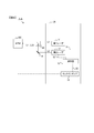
- FIG. 1 is an overall configuration diagram of the OPP-STM 1 according to the first embodiment.
- light is shown by a solid line and an electric signal is shown by a broken line.
- the OPP-STM1 is composed of a light output system 2 and an STM200.
- the optical output system 2 includes a first laser 11, a second laser 12, a calculator 13, a lock-in amplifier 14, a mirror M, and a beam splitter BS.
- the first laser 11 is a laser light source that outputs the first light L1 that is a laser light.
- the first laser 11 outputs the pulsed first light L1 after the first delay time.
- the second laser 12 is a laser light source that outputs the second light L2 that is a laser light.
- the pulse signal is input from the calculator 13, the second laser 12 outputs the pulsed second light L2 after the second delay time.
- the first delay time and the second delay time are substantially the same and very short time. The two do not have to match exactly, and the difference between the two is absorbed by the adjustment described later.
- the intensities of the first light L1 and the second light L2 may be the same or different.
- the pulse widths of the first light L1 and the second light L2 may be the same or different.
- the pulse widths of the first light L1 and the second light L2 may be fixed values or may be variable. When the pulse widths of the first light L1 and the second light L2 are variable, it may be changeable by manually operating the switches provided in the first laser 11 and the second laser 12, or the first laser may be changed. 11 and the second laser 12 may be changeable according to the pulse width of the pulse signal.
- the calculator 13 is a pulse signal generator, and is configured to include a voltage generation source and a calculator.
- the arithmetic unit 13 is realized by, for example, an FPGA (Field Programmable Gate Array) which is a rewritable logic circuit.
- the arithmetic unit 13 outputs a pulse signal to the first laser 11 and the second laser 12, and outputs a reference signal to the lock-in amplifier 14.
- a signal line connecting the calculator 13 and the first laser 11 is called S1
- a signal line connecting the calculator 13 and the second laser 12 is called S2
- a signal line connecting the calculator 13 and the lock-in amplifier 14 is called S3.
- the lock-in amplifier 14 processes the signal output by the STM 200, and uses the reference signal output by the arithmetic unit 13 to detect a weak signal included in the output signal of the STM 200.
- the detected weak signal may be stored inside the lock-in amplifier 14 or may be stored in a storage device outside the lock-in amplifier 14.
- Mirror M is a plane mirror.
- the mirror M has a position/orientation adjusting mechanism for coaxially adjusting the spectrum L11 and the spectrum L22 output from the beam splitter BS.
- the operator adjusts the position and orientation of the mirror M in advance while observing the spectrum L11 and the spectrum L22 so that the spectrum L11 and the spectrum L22 are coaxial.
- the position/orientation adjusting mechanism may be provided on the first laser 11 or the second laser 12.
- the spectrum L11 and the spectrum L22 are collectively referred to as "output light”.
- Beam splitter BS splits incident light into transmitted light and reflected light. Specifically, the beam splitter BS splits the first light L1 into a spectrum L11 which is a transmitted light and a spectrum L12 which is a reflected light, and the second light L2 is a spectrum L21 which is a transmitted light and a spectrum L2 which is a reflected light. Separate into L22.
- the beam splitter BS may be a so-called half mirror in which the transmitted light amount and the reflected light amount are 1:1 and the ratio of the transmitted light amount and the reflected light amount may be other than that.
- the spectrum L12 and the spectrum L21 are not used and therefore not shown.
- the beam splitter BS may also be provided with a position/orientation adjusting mechanism in order to coaxially adjust the spectrum L11 and the spectrum L22 output from the beam splitter BS. Then, for example, the position may be adjusted by adjusting the angle of the mirror M, and the angle may be adjusted by adjusting the angle of the beam splitter BS.
- the STM 200 is a scanning tunneling microscope (STM) that uses the laser light output from the first laser 11 and the second laser 12 as pump light and probe light. Although the configuration of the STM 200 will be described in detail later, the STM 200 outputs the detected signal to the lock-in amplifier 14.
- STM scanning tunneling microscope
- the laser beam L1 output from the first laser 11 is split into a spectrum L11 and a spectrum L12 by the beam splitter BS.
- the spectrum L11 that has passed through the beam splitter BS enters the STM 200.
- the laser beam L2 output from the second laser 12 is reflected by the plurality of mirrors M, and is split into the spectrum L21 and the spectrum L22 by the beam splitter BS.
- the spectrum L22 reflected by the beam splitter BS enters the STM 200.
- the spectrum L11 is also referred to as "pump light” L11
- the spectrum L22 is also referred to as "probe light” L22.
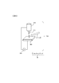
- FIG. 2 is a schematic diagram of the STM 200.
- the STM 200 includes a probe 210 and a tunnel current detector 220. Although the lock-in amplifier 14 is also shown in FIG. 2, it is shown by a broken line because it is not included in the configuration of the STM 200.
- a sample 900 is set in the STM 200.
- the spectrum L11 and the spectrum L22 emitted from the outside of the STM 200 are emitted to the surface of the sample 900 including the tip 211 of the probe 210.
- the sample 900 is excited when it is irradiated with the pump light L11, and is mainly irradiated with the probe light L22 while the sample 900 is excited.
- the probe light L22 is irradiated while the sample 900 is excited at at least one time difference.
- the number of optical carriers excited by the probe light L22 changes depending on the delay time, which is the difference between the timings at which the two spectra are irradiated to the sample 900, and the difference between the probe tip portion 51a and the surface of the sample 900 is changed.
- the tunnel current that flows in is changed and detected by the tunnel current detection unit 220.
- the tunnel current detector 220 outputs a signal of the detected current to the lock-in amplifier 14.
- FIG. 3 is a functional block diagram showing each function of the computing unit 13 as a functional block.
- the arithmetic unit 13 is realized by the FPGA.
- the FPGA reads the logic circuit information from the ROM (not shown) at the time of startup and writes it in the FPGA.
- the signal generation unit 132, the delay determination unit 133, the reference signal output unit 134, the input unit 135, and the storage unit 136 are formed.
- the delay determination unit 133 determines the value of the variable delay value 138 described later.
- the signal generator 132 includes a delay time counter and a voltage generator capable of generating a pulsed voltage.
- the reference signal output unit 134 includes a voltage generation source capable of generating a voltage signal.
- the input unit 135 includes a physical interface such as a button that receives a user command, or an electrical interface that receives a user command by an electric signal.
- the storage unit 136 stores a fixed delay value 137 and a variable delay value 138.
- the fixed delay value 137 and the variable delay value 138 may not be stored in the ROM (not shown), and in this case, the user inputs the values via the input unit 135 each time the arithmetic unit 13 is activated.
- the signal generator 132 outputs a pulse signal to the first laser 11 and the second laser 12.
- the delay determining unit 133 determines the variable delay value 138.
- the input unit 135 writes the value of the fixed delay value 137 in the storage unit 136 based on the input by the user.
- the delay value from the signal generator 132 outputting the pulse signal to the first laser 11 to the pulse signal outputting to the second laser 12, that is, the time interval, is the sum of the fixed delay value 137 and the variable delay value 138.
- the fixed delay value 137 is for canceling the influence of the optical path length, the length of the signal cable, and the individual difference between the first laser 11 and the second laser 12, and the fixed delay value 137 is set to an appropriate value.
- variable delay value 138 is a value that sets a difference in timing when the pump light L11 and the probe light L22 reach the sample 900.
- the variable delay value 138 is also referred to as “time difference ⁇ t”.
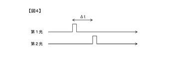
- FIG. 4 is a diagram showing an example of a temporal change in the light intensity of the spectrum L11 and the spectrum L22 at the position of the sample 900.
- time elapses from the left side to the right side in the drawing, and in the example shown in FIG. 4, the first light L11 reaches the sample 900 first, and then the second light L22 reaches the sample 900.
- the time difference ⁇ t has a positive value when the first light L11 reaches the sample 900 first, as shown in FIG.
- Measurement signal Before describing the operation of the calculator 13, an outline of the measurement signal of the STM 200 will be described to help understanding of the operation. However, the following description is for explaining typical measurement results when a sample having STM200 is used as a measurement target, and OPP-STM1 does not have the same tendency regardless of the type of sample. Absent.
- FIG. 5 is a diagram showing the relationship between the output signal of the STM 200 and the time difference ⁇ t.
- the sample 900 is excited by being irradiated with the pump light L11, and relaxes with the passage of time.
- the measured values when the time difference ⁇ t is t1, t2, and t3 are s13, s12, and s11, respectively, and the relationship of s13>s12>s11 is satisfied.
- the measurement signal decreases, and when the time difference ⁇ t is a certain value or more, that is, when the time difference ⁇ t is t6 or more in the example shown in FIG. 5, the measurement signal converges to the minimum value s0 in this measurement.
- the difference between the signal levels of s0 and s13 is smaller than the difference between the minimum value of the measurement signal, that is, the signal level between “0” on the vertical axis of FIG. 5 and the minimum measurement value s0.
- the lock-in amplifier 14 is used. By periodically using the lock-in amplifier 14 while switching the delay time ⁇ t, the measured values s13, s12, s11, etc. are evaluated by comparison with s0 instead of comparison with zero. This solves the problem of low SN ratio.
- t6 and s0 are not clear before the measurement, a sufficiently long time, for example, a time several times as long as the assumed attenuation time is used. It is widely used instead of t6. In the present embodiment, a sufficiently long time will be described as t9. Further, in the present embodiment, the values of s0 and s11 shown in FIG. 5 cannot be directly measured, and the relative value with respect to the reference s0, that is, the value of “s13-s0” or the value of “s12-s0”. Is obtained.
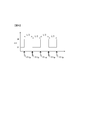
- FIG. 6 is a diagram showing the operation of the arithmetic unit 13 for obtaining s13 based on s0, that is, "s13-s0".
- the arrow Flip shown at the bottom of FIG. 6 indicates the timing at which the reference signal output from the calculator 13 to the lock-in amplifier 14 is inverted.
- the calculator 13 switches the time difference ⁇ t between t1 and t9 at every predetermined time L/2 that is half the time.
- the pump light L11 and the probe light L22 are output a plurality of times, for example, tens or hundreds of times.
- the signal generator 132 first outputs a pulse signal to the first laser 11, and outputs a pulse signal to the second laser 12 after the time of the sum of the fixed delay value 137 and the variable delay value 138 has elapsed from the output.
- the signal generator 132 measures the passage of time by counting the number of oscillations of an internal oscillator. That is, in the present embodiment, the fixed delay value 137 and the variable delay value 138 can be controlled in units of the oscillation cycle of the oscillator.
- the calculator 13 outputs the pump light L11 and the probe light L22 100 times over the time L/2 with the time difference ⁇ t being t9, and then outputs the output light 100 times over the time L/2 with the time difference ⁇ t being t1. ..
- the calculator 13 repeats this operation a plurality of times to realize the periodic change of ⁇ t shown in FIG.
- the arithmetic unit outputs -1V to the reference signal for the time period of L/2 where ⁇ t is t9, and outputs 1V to the reference signal for the time period of L/2 where ⁇ t is t1, thereby causing the lock-in amplifier 14 to operate.
- the output from the STM 200 oscillates between S0 and S13 in the cycle L according to the change in delay time.
- S13-S0 From the output of the lock-in amplifier that operates in synchronization with the reference signal, "S13-S0", which is the difference between S0 and S13, can be measured with a high SN ratio.
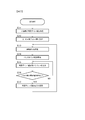
- FIG. 7 is a flowchart showing the operation of the arithmetic unit 13.
- the arithmetic unit 13 is realized by an FPGA, so the flowchart shown in FIG. 7 does not necessarily show the operation of the hardware faithfully.
- a counter circuit that counts the number of pulses and a circuit that generates an electric pulse when the counter has a specific value are always operating independently and in parallel, and their inputs and outputs are connected to each other. To be done.
- the operation of the arithmetic unit 13 will be described using a flowchart for convenience.
- the calculator 13 determines two variable delay values 138 that are periodically changed. This variable delay value 138 may be stored in the storage unit 136 in advance, or may be input by the user from the input unit 135 each time it is executed. In subsequent S312, the computing unit 13 sets one of the two types of variable delay values 138 set in S311 as the variable delay value 138 to be used, and proceeds to S313.
- the calculator 13 inverts the reference signal output to the lock-in amplifier 14. For example, if the reference signal was “ ⁇ 1V” until immediately before the execution of S313, the reference signal is changed to “+1V” in S313.
- the calculator 13 initializes a pulse counter for counting the number of pulses to zero.
- the arithmetic unit 13 causes the signal generation unit 132 to output the pulse signal to the first laser 11 and the second laser 12, using the currently set variable delay value 138.
- the calculator 13 increments the count number of the pulse counter by 1, and determines whether or not the count number of the pulse counter reaches a predetermined prescribed value, for example, 100.
- the arithmetic unit 13 proceeds to S317 when determining that the predetermined count has been reached, that is, when the time L/2 has elapsed since the execution of S314, and returns to S315 when determining that the predetermined count has not been reached.
- the computing unit 13 changes the variable delay value 138 to the other of the two types determined in S311, which is not the currently set value, and returns to S313.
- the arithmetic unit 13 further determines whether or not the number of times of processing reaches a predetermined number of times, and if it determines that the number of times of processing reaches a predetermined number of times, the operation unit 13 returns to S311 and sets two different variable delay values. Measurement may be continued and the process shown in FIG. 7 may be terminated.
- the optical output system 2 outputs a first laser 11 that outputs a first light L1 that is a pulse laser according to an input signal, and outputs a second light L2 that is a pulse laser according to an input signal.
- the second laser 12 and the calculator 13 for inputting signals to the first laser 11 and the second laser 12.
- the calculator 13 switches the variable delay value 138, which is the difference between the timing of inputting a signal to the first laser 11 and the timing of inputting a signal to the second laser 12, in a plurality of ways. Therefore, the timing at which the first laser 11 and the second laser 12 output the pulse laser can be switched with a simple configuration.
- the method of changing the optical path length in the prior art requires mechanical operations such as movement of the stage and driving of the mirror, and thus there is a problem that the occurrence of vibration is unavoidable, and the switching speed is physically limited. There is a problem. It is known to use a Pockels cell to solve these problems. However, although the Pockels cell can solve the above-mentioned two problems, it has a problem that light cannot be completely blocked and a device configuration becomes large.
- the problem of not being able to block light completely is that weak light leaks out when the light should be blocked. That is, weak light is always emitted, which has an unintended effect on the measured value.
- the problem that the device configuration becomes large is that the resolution of the delay time that can be set only with the Pockels cell is limited by the repetition period (up to 10 ns) of the original laser, so if a delay time resolution lower than that is required. That is, a mechanism is separately required to control the pulse output timings of the two lasers. If the control becomes complicated, the device becomes large in size, and the installation area of the device and the required cost also become large.
- the optical output system 2 can freely set the delay time by controlling the timing of the electric signals input to the first laser 11 and the second laser 12, so that the method of changing the optical path length or the method of using the Pockels cell is used. Such a problem does not occur.
- the light output system 2 has the advantages that there is no vibration, there is no limit on the switching speed, there is no unnecessary weak light pulse irradiation between pulses, and the device configuration is simple and the installation area is small. Have.
- the calculator 13 includes a reference signal output unit 134 that changes the variable delay value 138 in two ways at a predetermined cycle L and outputs a reference signal indicating a timing for changing the variable delay value. Therefore, on the assumption that the lock-in amplifier 14 is used, necessary information can be acquired from the weak signal output from the STM 200.
- the optical output system 2 includes the lock-in amplifier 14 that performs the lock-in detection using the reference signal, with the output of the STM 200 using the first light L1 and the second light L2 as a processing target. Therefore, necessary information can be acquired from the weak signal output from the STM 200.
- the light output system 2 includes a beam splitter BS that coaxially outputs at least a part of the first light L1 and at least a part of the second light L2 as output light. If the output of the light output system 2 has the different optical axes of the first light L1 and the second light L2, they must be coaxial depending on the measurement system used. Since it is coaxial, it has the advantage of being easy to use.
- the optical pump/probe scanning tunneling microscope system 1 includes a light output system 2, a part of the first light L1 and a part of the second light L2 output from the light output system 2, and a pump light L11 and a probe.
- the arithmetic unit 13 is realized by the FPGA.
- the arithmetic unit 13 may be realized by a combination of a CPU that is a central processing unit instead of the FPGA, a ROM that is a read-only storage area, and a RAM that is a readable/writable storage area.
- the CPU stores the program stored in the ROM in the RAM and executes the program.
- the arithmetic unit 13 may be realized by an ASIC (Application Specific Integrated Circuit) which is an integrated circuit for a specific application, instead of the FPGA.
- the arithmetic unit 13 may be realized by a combination of different configurations, for example, a combination of CPU, ROM, RAM and FPGA.
- the variable delay value 138 which is the difference between the timing of inputting the signal and the timing of inputting the signal to the second laser 12, and the output of the reference signal indicating the timing of changing the variable delay value 138.
- the present invention also includes a program for an FPGA circuit that enables the same operation as the above program.
- the light output system 2 may not include the lock-in amplifier 14. In this case, the calculator 13 does not output the pulse signal to the lock-in amplifier 14.
- the lock-in amplifier 14 may be external to the light output system 2.
- the calculator 13 outputs a pulse signal to the lock-in amplifier 14 existing outside the optical output system 2.
- the measuring device used in combination with the light output system 2 is not limited to the STM 200. Any measuring device may be used as long as it is a pump/probe method.
- the light output system 2 may include a plurality of mirrors M to increase the degree of freedom of arrangement and adjustment.
- the first laser 11, the beam splitter BS, and the second laser 11 are further adjusted so that the optical path length from the first laser 11 to the beam splitter BS and the optical path length from the second laser 12 to the beam splitter BS can be adjusted. 12, and a plurality of mirrors M may be arranged.
- the computing unit 13 may include an input interface, and may be configured such that the user can input or adjust the fixed delay value 137.
- the calculator 13 may include a volume switch, and the user may increase or decrease the fixed delay value 137 according to the rotation direction and the rotation amount of the volume switch.
- FIG. 1 A second embodiment of the optical pump-probe scanning tunneling microscope system will be described with reference to FIG.
- the same components as those of the first embodiment are designated by the same reference numerals, and the differences are mainly described.
- the points that are not particularly described are the same as those in the first embodiment.
- the present embodiment differs from the first embodiment mainly in that the optical output system outputs two laser beams independently and the two laser beams are coaxial with each other outside the optical output system.
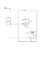
- FIG. 8 is an overall configuration diagram of an optical pump/probe scanning tunneling microscope system 1A according to the second embodiment. The difference from the first embodiment is that the mirror M and the beam splitter BS are not included in the optical output system 2A. Other configurations are similar to those of the first embodiment.
- the measuring device combined with the optical output system 2A measures the pump-probe method using non-coaxial light. Further, even when the measurement is performed by the pump-probe method using the coaxial light, the same effect can be obtained by using the mirror M and the beam splitter BS as in the first embodiment.
- FIG. 1 A third embodiment of the optical pump-probe scanning tunneling microscope system will be described with reference to FIG.
- the same components as those of the first embodiment are designated by the same reference numerals, and the differences are mainly described.
- the points that are not particularly described are the same as those in the first embodiment.
- the present embodiment is different from the first embodiment mainly in that the optical output system outputs two laser beams without making them coaxial.
- FIG. 9 is an overall configuration diagram of an optical pump/probe scanning tunneling microscope system 1B according to the third embodiment.
- the difference from the first embodiment is that the beam splitter and the mirror are not provided. That is, in the present embodiment, the output light L1 and the output light L2 are directly input to the STM 200.
- the measuring device combined with the optical output system 2A measures the pump-probe method using non-coaxial light.
- FIG. 1 A fourth embodiment of the optical pump/probe scanning tunneling microscope system will be described with reference to FIG.
- the same components as those of the first embodiment are designated by the same reference numerals, and the differences are mainly described.
- the points that are not particularly described are the same as those in the first embodiment.
- the present embodiment is different from the first embodiment mainly in that highly accurate control of the time difference ⁇ t is possible.
- the oscillation time per oscillation of the oscillator included in the computing unit 13 is sufficiently shorter than the required timekeeping accuracy. However, if the condition that the oscillation time per oscillation of the oscillator included in the computing unit 13 is sufficiently short compared with the required timekeeping accuracy is not satisfied, it is effective to use the analog delay circuit described below together. is there.
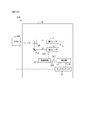
- FIG. 10 is an overall configuration diagram of an optical pump/probe scanning tunneling microscope system 1C according to the fourth embodiment.
- the optical pump/probe scanning tunneling microscope system 1C comprises a light output system 2C and an STM 200.
- the difference between the optical output system 2C and the optical output system 2 is that the optical output system 2C further includes a delay circuit 18.
- the output of the pulse signal from the calculator 13 to the second laser 12 is performed via the delay circuit 18.
- the delay time in the delay circuit 18 can be adjusted by the control signal from the calculator 13 through S25.
- the delay circuit 18 can adjust the delay time in units of ps, for example.
- the delay circuit 18 outputs the pulse signal to the second laser 12 through S22 with a delay time set by the characteristics of the analog circuit.
- the time difference ⁇ t it is possible to control the time difference ⁇ t with higher accuracy.
- the frequency of the oscillator provided in the arithmetic unit 13 is 1 GHz
- one cycle is 1 ns, so that control in units of ps, which is a time less than one cycle, cannot be realized.
- the delay circuit 18 the time difference ⁇ t can be controlled with a resolution of a time shorter than one cycle of the oscillator included in the calculator 13.
- the delay circuit 18 may be configured integrally with the calculator 13. For example, by using the FPGA including the output delay circuit, the arithmetic unit 13 including the delay circuit 18 can be realized.
- FIG. 1 A fifth embodiment of the optical pump/probe scanning tunneling microscope system will be described with reference to FIG.
- the same components as those of the first embodiment are designated by the same reference numerals, and the differences are mainly described.
- the points that are not particularly described are the same as those in the first embodiment.
- This embodiment is different from the first embodiment mainly in that the first laser continues to output a pulse laser at a predetermined cycle without receiving a signal from the outside.
- FIG. 11 is an overall configuration diagram of an optical pump/probe scanning tunneling microscope system 1D according to the fifth embodiment.
- the difference from the first embodiment is that a first laser 11A that operates independently is provided instead of the first laser 11, and two beams that split the first light L1 that is the output of the first laser 11A.
- the points are that the splitters BS1 and BS2 are provided, and that the photodetector 15 that detects the output of the first laser 11A is provided.
- the operation of the calculator 13 is also different from that of the first embodiment.
- the frequency at which the first laser 11A outputs a pulse laser is known, and is 100 kHz, for example. However, this frequency is not always exact, and perfect synchronization cannot be expected at least with the oscillator incorporated in the arithmetic unit 13.
- the photodetector 15 converts the received light into an electric signal and outputs it.
- the photodetector 15 may be realized using a photomultiplier tube or a photodiode using a semiconductor pn junction.
- the light detector 15 is supplied with the spectrum L12 which is a part of the first light L1 output from the first laser 11.
- the photodetector 15 outputs the electric signal obtained by converting the received light to the calculator 13 as a synchronization signal S5.
- the arithmetic unit 13 generates a clock several hundred to several thousand times with the synchronization signal S5 as a reference timing, and uses it to count the variable delay value 138. For example, when the output of the first laser 11A is 100 kHz, the calculator 13 generates a 100 MHz clock and counts the variable delay value 138 with reference to the reception time of the synchronization signal S5.
- the light output system 2D includes a first laser 11A that outputs a first light L1 that is an optical pulse at a predetermined cycle, and a second laser that outputs a second light that is a pulse laser according to an input signal. 12 and a calculator 13 that inputs a signal to the second laser 12 with reference to the timing at which the first light L1 is output.
- the calculator 13 switches the variable delay value 138, which is the difference between the timing at which the first light L1 is output and the timing at which a signal is input to the second laser 12, in a plurality of ways.
- the second laser 12 that outputs a pulse laser in response to the input pulse signal does not necessarily have a high output, so that the configuration of the present embodiment has the further advantage that a high-output laser oscillator can be used.
- the first device 1011 may output something other than a laser.
- the first device 1011 may be a synchrotron and may output X-ray pulses at a predetermined cycle.
- FIG. 1 A sixth embodiment of the optical pump-probe scanning tunneling microscope system will be described with reference to FIG.
- the same components as those of the first embodiment are designated by the same reference numerals, and the differences are mainly described.
- the points that are not particularly described are the same as those in the first embodiment.
- the present embodiment differs from the first embodiment mainly in that the output timing of the electric signal from the signal generating unit 132 is specified.
- the hardware configuration of the optical pump/probe scanning tunneling microscope system in the sixth embodiment is the same as that in the first embodiment, and the description thereof is omitted.
- the functional configuration of the optical pump/probe scanning tunneling microscope system according to the sixth embodiment is the same as that of the first embodiment except for the details of the mounting of the signal generator 132.
- the operation of the signal generator 132 and the calculator 13 including the signal generator 132 will be described below.
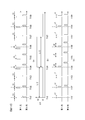
- FIG. 12 is a diagram for explaining the operation of the arithmetic unit 13 in the sixth embodiment.
- FIG. 12A is a diagram showing an operation of the arithmetic unit 13 in the sixth embodiment
- FIG. 12B is a diagram showing a reference signal
- FIG. 12C is a diagram showing an operation of a comparative example. 12A to 12C, the time axis in the horizontal direction in the figure is synchronized.
- each of the first light L1 and the second light L2 is output only three times on average in the time of L/2, which is half the modulation period. 12, T101, T102, T103,... Are times at which the length of L/2 is divided into N, with the start time of the modulation period L being the reference, in the example shown in FIG. Below, each of these T101, T102, etc. is called "reference time.”
- the signal generator 132 sets the second light L2 to the first light L1 before the reference time such as T101 or T102 by half the variable delay value 138. Is shifted backward by half the value of the variable delay value 138, and the time difference between the two reaching the sample 900 is set as the variable delay value 138. For example, when the variable delay value 138 is t1, the first light beam L1 arrives t1/2 earlier than the reference time, and the second light beam L2 arrives later t1/2 later than the reference time. And outputs a signal to the second laser 12.
- variable delay value 138 When the variable delay value 138 is t9, L1 reaches the first laser 11 and the second laser 12 so that L1 arrives earlier than the reference time by t9/2 and L2 arrives later than the reference time by t9/2. Output a signal.
- the signal generation unit 132 makes sure that the first light L1 always arrives at the reference time and the second light L2 arrives after a delay of the variable delay value 138 from the reference time. By operating them, the time difference between the two reaching the sample 900 is set as the variable delay value 138.
- the difference between the two becomes noticeable before and after the time when the variable delay value is switched.
- the density of the total number of light pulses of the first light L1 and the second light L2 in the time direction is substantially constant before and after the switching, and there is no temporal density.
- the density of the number of light pulses of the first light L1 in the time direction is completely constant regardless of time, but for the second light L2, the light irradiated to the sample 900 is temporally before and after T104. It becomes coarse, and the light irradiated to the sample 900 becomes dense in time before and after T107.
- the output of the STM 200 includes not only the effect of changing the variable delay value 138 for each half cycle of the modulation period L but also the effect of the temporal density of the emitted light generated for each half cycle.
- the present embodiment has an advantage that the influence of the variable delay value 138 can be easily measured because the density of the light with which the sample 900 is irradiated is less likely to occur before and after the modulation.
- the following operational effects can be obtained.
- the average time of the timing at which the first light L1 reaches the sample 900 and the timing at which the second light L2 reaches the sample 900 matches the reference time based on the modulation timing of the reference signal.
- the signal is output to the first laser 11 and the second laser 12 so as to do so. Therefore, before and after the change of the variable delay value 138, the density of the light irradiating the sample 900 hardly occurs, and the influence of the variable delay value 138 can be easily measured.
Landscapes
- Physics & Mathematics (AREA)
- Health & Medical Sciences (AREA)
- General Health & Medical Sciences (AREA)
- General Physics & Mathematics (AREA)
- Nuclear Medicine, Radiotherapy & Molecular Imaging (AREA)
- Analytical Chemistry (AREA)
- Life Sciences & Earth Sciences (AREA)
- Chemical & Material Sciences (AREA)
- Biochemistry (AREA)
- Immunology (AREA)
- Pathology (AREA)
- Radiology & Medical Imaging (AREA)
- Spectroscopy & Molecular Physics (AREA)
- Optics & Photonics (AREA)
- Nonlinear Science (AREA)
- Microscoopes, Condenser (AREA)
- Investigating Or Analysing Materials By Optical Means (AREA)
- Investigating, Analyzing Materials By Fluorescence Or Luminescence (AREA)
Abstract
Description
本発明の第2の態様による測定システムは、上述する光出力システムと、前記光出力システムから出力される前記第1光の少なくとも一部および前記第2光の少なくとも一部をポンプ光およびプローブ光としてポンプ・プローブ法による測定を行う測定系とを備える。
本発明の第3の態様による光学的ポンプ・プローブ走査トンネル顕微鏡システムは、上述する光出力システムと、前記光出力システムから出力される前記第1光の少なくとも一部および前記第2光の少なくとも一部をポンプ光およびプローブ光として利用する光学的ポンプ・プローブ走査トンネル顕微鏡とを備える。
本発明の第4の態様による演算器は、入力された信号に応じてパルスレーザである第1光を出力する第1レーザ、および入力された信号に応じてパルスレーザである第2光を出力する第2レーザとともに用いられる演算器であって、第1レーザおよび第2レーザに信号を入力する信号発生部と、第1レーザに信号を入力するタイミングと、第2レーザに信号を入力するタイミングとの差である可変ディレイ値を複数とおりに切り替えて前記信号を繰り返し入力するディレイ決定部と、可変ディレイ値を変化させるタイミングを示す参照信号を出力する信号出力部とを備える。
本発明の第5の態様によるプログラムは、入力された信号に応じてパルスレーザである第1光を出力する第1レーザ、および入力された信号に応じてパルスレーザである第2光を出力する第2レーザとともに用いられる演算器に、第1レーザおよび第2レーザに信号を入力することと、第1レーザに信号を入力するタイミングと、第2レーザに信号を入力するタイミングとの差である可変ディレイ値を複数とおりに切り替えて前記信号を繰り返し入力することと、可変ディレイ値を変化させるタイミングを示す参照信号を出力させることとを実行させる。
本発明の第6の態様による光出力システムは、所定の周期で光パルスである第1光を出力する第1装置と、入力された信号に応じてパルスレーザである第2光を出力する第2装置と、第1光が出力されるタイミングを基準として第2装置に信号を入力する演算器とを備え、演算器は、第1光が出力されるタイミングと、第2装置に信号を入力するタイミングとの差である可変ディレイ値を複数とおりに切り替えて前記信号を繰り返し入力する。
以下、図1~図7を参照して、OPP-STM(Optical Pump-Probe Scanning Tunneling Microscopy;光学的ポンプ・プローブ走査トンネル顕微鏡)の第1の実施の形態を説明する。
図1は第1の実施の形態におけるOPP-STM1の全体構成図である。図1では光を実線で示し、電気信号を破線で示している。
図2は、STM200の模式図である。STM200は、探針210と、トンネル電流検出部220と、を備える。なお図2にはロックインアンプ14も記載しているが、STM200の構成には含まれないので破線で示している。STM200には試料900がセットされる。STM200の外部から照射される分光L11および分光L22は、探針210の先端211を含む試料900の表面に照射される。試料900はポンプ光L11が照射されると励起され、主に試料900が励起されている間にプローブ光L22が照射される。
図3は、演算器13が有する各機能を機能ブロックとして表した機能ブロック図である。前述のとおり演算器13はFPGAにより実現される。FPGAは起動時に不図示のROMから論理回路情報を読み込んでFPGA内に書き込む。この書き込みにより、信号発生部132と、ディレイ決定部133と、参照信号出力部134と、入力部135と、記憶部136とが形成される。ディレイ決定部133は、後述する可変ディレイ値138の値を決定する。信号発生部132は、遅延時間の計数部およびパルス状の電圧を発生可能な電圧発生源を含む。参照信号出力部134は電圧信号を発生可能な電圧発生源を含む。
図4は試料900の位置における分光L11および分光L22の光強度の時間変化の例を示す図である。図4では図示左側から右側に向かって時間が経過しており、図4に示す例では第1光L11が先に試料900に到達し、その後に第2光L22が試料900に到達した。本実施の形態では、図4に示すように第1光L11が先に試料900に到達する場合に時間差Δtが正の値をとることとする。
演算器13の動作を説明する前に、その動作の理解を助けるためにSTM200の測定信号の概要を説明する。ただし以下の説明はSTM200がある試料を測定対象とした際の代表的な測定結果を説明するものであり、試料の種類を問わず同様の傾向を有することをOPP-STM1の前提とするものではない。
図6は、s0を基準としたs13、すなわち「s13-s0」を得るための演算器13の動作を示す図である。図6では図示左から右に向かって時間が経過しており、縦軸は時間差Δtを示している。図6下部に示す矢印Flipは、演算器13がロックインアンプ14に出力する参照信号が反転するタイミングを示している。図6に示す例では演算器13は、変調周期をLとすると、その半分の時間である所定の時間L/2ごとに時間差Δtをt1とt9とに切り替える。所定の時間L/2において、ポンプ光L11やプローブ光L22は複数回、たとえば数十回や数百回出力される。
図7は、演算器13の動作を示すフローチャートである。なお本実施の形態では演算器13はFPGAにより実現されるため、図7に示すフローチャートはハードウエアの動作を必ずしも忠実には示していない。たとえば実際にはパルス数をカウントするカウンタ―回路と、カウンタが特定の値の場合に電気パルスを発生させる回路などが常時独立して並列に動作しており、それらの入力や出力が相互に接続される。本実施の形態では、便宜的にフローチャートを用いて演算器13の動作を説明する。
(1)光出力システム2は、入力された信号に応じてパルスレーザである第1光L1を出力する第1レーザ11と、入力された信号に応じてパルスレーザである第2光L2を出力する第2レーザ12と、第1レーザ11および第2レーザ12に信号を入力する演算器13とを備える。演算器13は、第1レーザ11に信号を入力するタイミングと、第2レーザ12に信号を入力するタイミングとの差である可変ディレイ値138を複数とおりに切り替える。そのため第1レーザ11と第2レーザ12がパルスレーザを出力するタイミングを簡易な構成で切り替えることができる。
上述した第1の実施の形態では、演算器13は、FPGAにより実現された。しかし演算器13の少なくとも一部は、FPGAの代わりに中央演算装置であるCPU、読み出し専用の記憶領域であるROM、および読み書き可能な記憶領域であるRAMの組み合わせによって実現されてもよい。この場合にはROMに格納されるプログラムをCPUがRAMに展開して実行する。また演算器13は、FPGAの代わりに特定用途向け集積回路であるASIC(Application Specific Integrated Circuit)により実現されてもよい。さらに演算器13は、異なる構成の組み合わせ、たとえばCPU、ROM、およびRAMとFPGAの組み合わせにより実現されてもよい。
(6)第1レーザ11、および第2レーザ12とともに用いられる演算器13が実行するプログラムであって、第1レーザ11および第2レーザ12に信号を入力することと、第1レーザ11に信号を入力するタイミングと、第2レーザ12に信号を入力するタイミングとの差である可変ディレイ値138を複数とおりに切り替えることと、可変ディレイ値138を変化させるタイミングを示す参照信号を出力させることとを実行させるプログラム。
光出力システム2は、ロックインアンプ14を備えなくてもよい。この場合は演算器13はロックインアンプ14にパルス信号を出力しない。
ロックインアンプ14は光出力システム2の外部に存在してもよい。この場合は演算器13は、光出力システム2の外部に存在するロックインアンプ14にパルス信号を出力する。
光出力システム2と組み合わせて利用する計測装置は、STM200に限定されない。ポンプ・プローブ法による測定を行う計測装置であればよい。
図1に示した光出力システム2の構成では、ミラーMは1つのみ含まれた。しかし光出力システム2は、配置や調整の自由度を上げるために複数のミラーMを備えてもよい。この場合はさらに、第1レーザ11からビームスプリッタBSまでの光路長と第2レーザ12からビームスプリッタBSまでの光路長が調整可能となるように、第1レーザ11、ビームスプリッタBS、第2レーザ12、および複数のミラーMを配置してもよい。
演算器13は、入力インタフェースを備え、固定ディレイ値137をユーザが入力や調整可能に機構されてもよい。たとえば演算器13はボリュームスイッチを備え、ユーザがボリュームスイッチの回転方向および回転量に合わせて固定ディレイ値137を増減してもよい。
図8を参照して、光学的ポンプ・プローブ走査トンネル顕微鏡システムの第2の実施の形態を説明する。以下の説明では、第1の実施の形態と同じ構成要素には同じ符号を付して相違点を主に説明する。特に説明しない点については、第1の実施の形態と同じである。本実施の形態では、主に、光出力システムが2つのレーザ光を独立して出力し、光出力システムの外部で2つのレーザ光を同軸にする点で、第1の実施の形態と異なる。
図9を参照して、光学的ポンプ・プローブ走査トンネル顕微鏡システムの第3の実施の形態を説明する。以下の説明では、第1の実施の形態と同じ構成要素には同じ符号を付して相違点を主に説明する。特に説明しない点については、第1の実施の形態と同じである。本実施の形態では、主に、光出力システムが2つのレーザ光を同軸とせずに出力する点で、第1の実施の形態と異なる。
図10を参照して、光学的ポンプ・プローブ走査トンネル顕微鏡システムの第4の実施の形態を説明する。以下の説明では、第1の実施の形態と同じ構成要素には同じ符号を付して相違点を主に説明する。特に説明しない点については、第1の実施の形態と同じである。本実施の形態では、主に、高精度な時間差Δtの制御が可能な点で、第1の実施の形態と異なる。
遅延回路18は、演算器13と一体に構成されていてもよい。たとえば出力遅延回路を備えるFPGAを用いることで、遅延回路18を内蔵する演算器13を実現できる。
図11を参照して光学的ポンプ・プローブ走査トンネル顕微鏡システムの第5の実施の形態を説明する。以下の説明では、第1の実施の形態と同じ構成要素には同じ符号を付して相違点を主に説明する。特に説明しない点については、第1の実施の形態と同じである。本実施の形態では、主に、第1レーザが外部から信号を入力されることなく、所定の周期でパルスレーザを出力し続ける点が第1の実施の形態と異なる。
(7)光出力システム2Dは、所定の周期で光パルスである第1光L1を出力する第1レーザ11Aと、入力された信号に応じてパルスレーザである第2光を出力する第2レーザ12と、第1光L1が出力されるタイミングを基準として第2レーザ12に信号を入力する演算器13とを備える。演算器13は、第1光L1が出力されるタイミングと、第2レーザ12に信号を入力するタイミングとの差である可変ディレイ値138を複数とおりに切り替える。そのため、従来から用いられている所定の周期でレーザ光を出力するレーザ発振器を用いて第1の実施の形態と同様の作用効果を得ることができる。入力されたパルス信号に応じてパルスレーザを出力する第2レーザ12などは、出力が必ずしも高くないため、本実施の形態の構成であれば高出力のレーザ発振器を利用できるというさらなる利点を有する。
第1装置1011は、レーザ以外を出力してもよい。たとえば第1装置1011がシンクロトロンであり、所定の周期でX線パルスを出力してもよい。
図12を参照して光学的ポンプ・プローブ走査トンネル顕微鏡システムの第6の実施の形態を説明する。以下の説明では、第1の実施の形態と同じ構成要素には同じ符号を付して相違点を主に説明する。特に説明しない点については、第1の実施の形態と同じである。本実施の形態では、主に、信号発生部132からの電気信号の出力タイミングを特定している点で第1の実施の形態と異なる。
(8)信号発生部132は、第1光L1が試料900に到達するタイミングと第2光L2が試料900に到達するタイミングの平均時刻が、参照信号の変調タイミングを基準とする基準時刻に一致するように第1レーザ11および第2レーザ12に信号を出力する。そのため、可変ディレイ値138の変化の前後でも試料900に照射される光の粗密が起こりにくく、可変ディレイ値138の影響を測定しやすい。
日本国特許出願2018-233878(2018年12月13日出願)
2、2A…光出力システム
3…演算器
11…第1レーザ
12…第2レーザ
13…演算器
14…ロックインアンプ
15…光検出器
131…調整部
132…信号発生部
133…ディレイ決定部
134…参照信号出力部
135…入力部
136…記憶部
137…固定ディレイ値
138…可変ディレイ値
900…試料
L1…第1光
L11…ポンプ光
L2…第2光
L22…プローブ光
Claims (12)
- 入力された信号に応じてパルスレーザである第1光を出力する第1レーザと、
入力された信号に応じてパルスレーザである第2光を出力する第2レーザと、
前記第1レーザおよび前記第2レーザに信号を入力する演算器とを備え、
前記演算器は、前記第1レーザに信号を入力するタイミングと、前記第2レーザに信号を入力するタイミングとの差である可変ディレイ値を複数とおりに切り替えて前記信号を繰り返し入力する光出力システム。 - 請求項1に記載の光出力システムにおいて、
前記演算器は、前記可変ディレイ値を2通りに所定の周期で変化させ、
前記可変ディレイ値を変化させるタイミングを示す参照信号を出力する参照信号出力部をさらに備える光出力システム。 - 請求項2に記載の光出力システムにおいて、
前記第1光および前記第2光を用いた測定系の出力を処理対象とし、前記参照信号を用いてロックイン検出を行うロックインアンプをさらに備える光出力システム。 - 請求項1に記載の光出力システムにおいて、
前記第1光の少なくとも一部、および前記第2光の少なくとも一部を出力光として同軸に出力する光学系をさらに備える光出力システム。 - 請求項1から請求項4までのいずれか一項に記載の光出力システムと、
前記光出力システムから出力される前記第1光の少なくとも一部および前記第2光の少なくとも一部をポンプ光およびプローブ光としてポンプ・プローブ法による試料の測定を行う測定系とを備える測定システム。 - 請求項2または請求項3に従属する請求項5に記載の測定システムにおいて、
前記演算器は、前記可変ディレイ値を決定するディレイ決定部と、前記ディレイ決定部が決定した前記可変ディレイ値に基づいて、前記第1レーザおよび前記第2レーザに信号を入力する信号発生部を含んで構成され、
前記信号発生部は、前記第1光の少なくとも一部が前記試料に到達するタイミングと第2光が前記試料に到達するタイミングの平均時刻が、前記参照信号により示される前記可変ディレイ値を変化させるタイミングを基準とする基準時刻に一致するように前記第1レーザおよび前記第2レーザに信号を出力する測定システム。 - 請求項1から請求項4までのいずれか一項に記載の光出力システムと、
前記光出力システムから出力される前記第1光の少なくとも一部および前記第2光の少なくとも一部をポンプ光およびプローブ光として利用し試料の測定を行う光学的ポンプ・プローブ走査トンネル顕微鏡とを備える光学的ポンプ・プローブ走査トンネル顕微鏡システム。 - 請求項2または請求項3に従属する請求項7に記載の光学的ポンプ・プローブ走査トンネル顕微鏡システムにおいて、
前記演算器は、前記可変ディレイ値を決定するディレイ決定部と、前記ディレイ決定部が決定した前記可変ディレイ値に基づいて、前記第1レーザおよび前記第2レーザに信号を入力する信号発生部を含んで構成され、
前記信号発生部は、前記第1光の少なくとも一部が前記試料に到達するタイミングと第2光が前記試料に到達するタイミングの平均時刻が、前記参照信号により示される前記可変ディレイ値を変化させるタイミングを基準とする基準時刻に一致するように前記第1レーザおよび前記第2レーザに信号を出力する光学的ポンプ・プローブ走査トンネル顕微鏡システム。 - 入力された信号に応じてパルスレーザである第1光を出力する第1レーザ、および入力された信号に応じてパルスレーザである第2光を出力する第2レーザとともに用いられる演算器であって、
前記第1レーザおよび前記第2レーザに信号を入力する信号発生部と、
前記第1レーザに信号を入力するタイミングと、前記第2レーザに信号を入力するタイミングとの差である可変ディレイ値を複数とおりに切り替えて前記信号を繰り返し入力するディレイ決定部と、
前記可変ディレイ値を変化させるタイミングを示す参照信号を出力する信号出力部とを備える演算器。 - 入力された信号に応じてパルスレーザである第1光を出力する第1レーザ、および入力された信号に応じてパルスレーザである第2光を出力する第2レーザとともに用いられる演算器に、
前記第1レーザおよび前記第2レーザに信号を入力することと、
前記第1レーザに信号を入力するタイミングと、前記第2レーザに信号を入力するタイミングとの差である可変ディレイ値を複数とおりに切り替えて前記信号を繰り返し入力することと、
前記可変ディレイ値を変化させるタイミングを示す参照信号を出力させることとを実行させるためのプログラム。 - 所定の周期で光パルスである第1光を出力する第1装置と、
入力された信号に応じてパルスレーザである第2光を出力する第2装置と、
前記第1光が出力されるタイミングを基準として前記第2装置に信号を入力する演算器とを備え、
前記演算器は、第1光が出力されるタイミングと、前記第2装置に信号を入力するタイミングとの差である可変ディレイ値を複数とおりに切り替えて前記信号を繰り返し入力する光出力システム。 - 入力された信号に応じてパルスレーザである第1光を出力する第1レーザ、および入力された信号に応じてパルスレーザである第2光を出力する第2レーザとともに用いられる演算器が実行する演算方法であって、
前記第1レーザおよび前記第2レーザに信号を入力することと、
前記第1レーザに信号を入力するタイミングと、前記第2レーザに信号を入力するタイミングとの差である可変ディレイ値を複数とおりに切り替えて前記信号を繰り返し入力することと、
前記可変ディレイ値を変化させるタイミングを示す参照信号を出力させることとを含む演算方法。
Priority Applications (5)
| Application Number | Priority Date | Filing Date | Title |
|---|---|---|---|
| US17/312,844 US12222365B2 (en) | 2018-12-13 | 2019-11-29 | Optical output system, measurement system, optical pump-probe scanning tunneling microscope system, computing device, program, and computing method |
| JP2020559151A JP6964366B2 (ja) | 2018-12-13 | 2019-11-29 | 光出力システム、測定システム、光学的ポンプ・プローブ走査トンネル顕微鏡システム、演算器、プログラム、演算方法 |
| EP19895256.6A EP3896462A4 (en) | 2018-12-13 | 2019-11-29 | OUTPUT OPTICAL SYSTEM, MEASUREMENT SYSTEM, PUMP PROBE OPTICAL TUNNEL MICROSCOPE SYSTEM, COMPUTING DEVICE, PROGRAM AND COMPUTING METHOD |
| CN201980082262.8A CN113167811B (zh) | 2018-12-13 | 2019-11-29 | 光输出系统、测量系统、光学泵浦探测扫描隧道显微镜系统、运算器、程序、运算方法 |
| KR1020217021888A KR102660600B1 (ko) | 2018-12-13 | 2019-11-29 | 광출력 시스템, 측정 시스템, 광학적 펌프·프로브 주사 터널 현미경 시스템, 연산기, 프로그램, 연산 방법 |
Applications Claiming Priority (2)
| Application Number | Priority Date | Filing Date | Title |
|---|---|---|---|
| JP2018-233878 | 2018-12-13 | ||
| JP2018233878 | 2018-12-13 |
Publications (1)
| Publication Number | Publication Date |
|---|---|
| WO2020121856A1 true WO2020121856A1 (ja) | 2020-06-18 |
Family
ID=71076948
Family Applications (1)
| Application Number | Title | Priority Date | Filing Date |
|---|---|---|---|
| PCT/JP2019/046904 Ceased WO2020121856A1 (ja) | 2018-12-13 | 2019-11-29 | 光出力システム、測定システム、光学的ポンプ・プローブ走査トンネル顕微鏡システム、演算器、プログラム、演算方法 |
Country Status (6)
| Country | Link |
|---|---|
| US (1) | US12222365B2 (ja) |
| EP (1) | EP3896462A4 (ja) |
| JP (3) | JP6964366B2 (ja) |
| KR (1) | KR102660600B1 (ja) |
| CN (1) | CN113167811B (ja) |
| WO (1) | WO2020121856A1 (ja) |
Citations (9)
| Publication number | Priority date | Publication date | Assignee | Title |
|---|---|---|---|---|
| US20030184328A1 (en) * | 2002-03-26 | 2003-10-02 | Jongjoo Lee | Near-field probe for use in scanning system |
| JP2008139028A (ja) * | 2006-11-29 | 2008-06-19 | Japan Science & Technology Agency | ポンププローブ測定装置及びそれを用いた走査プローブ顕微鏡装置 |
| WO2013018813A1 (ja) * | 2011-08-02 | 2013-02-07 | 独立行政法人科学技術振興機構 | ポンププローブ測定装置 |
| JP2014518387A (ja) * | 2011-06-29 | 2014-07-28 | エコール ポリテクニーク/デジェアエル | ポンプ・プローブ分光法におけるパルス管理装置 |
| JP2014175442A (ja) | 2013-03-08 | 2014-09-22 | Dainippon Screen Mfg Co Ltd | 検査装置および検査方法 |
| JP2017003338A (ja) * | 2015-06-08 | 2017-01-05 | 日本電信電話株式会社 | モード結合比率分布測定方法及びモード結合比率分布測定装置 |
| JP2018179506A (ja) * | 2017-04-03 | 2018-11-15 | 花王株式会社 | 拡散反射スペクトル測定装置 |
| JP2018175999A (ja) * | 2017-04-03 | 2018-11-15 | 花王株式会社 | 光触媒活性の評価方法 |
| WO2019142914A1 (ja) * | 2018-01-19 | 2019-07-25 | Gセラノスティックス株式会社 | 走査プローブ顕微鏡 |
Family Cites Families (4)
| Publication number | Priority date | Publication date | Assignee | Title |
|---|---|---|---|---|
| WO2007132540A1 (ja) * | 2006-05-15 | 2007-11-22 | Osaka University | パルスレーザ光のタイミング調整装置、調整方法及び光学顕微鏡 |
| JP6386655B2 (ja) * | 2015-03-03 | 2018-09-12 | 株式会社日立ハイテクノロジーズ | テラヘルツ波発生装置及びそれを用いた分光装置 |
| FR3042609B1 (fr) * | 2015-10-19 | 2018-02-16 | Amplitude Systemes | Systeme optique non lineaire de generation ou d'amplification d'impulsions lumineuses par melange a n ondes comportant un dispositif de modulation rapide |
| EP3264540B1 (en) * | 2016-07-01 | 2020-02-26 | Deutsches Elektronen-Synchrotron DESY | Device and method for determining a temporal relationship of laser pulses, and applications thereof |
-
2019
- 2019-11-29 KR KR1020217021888A patent/KR102660600B1/ko active Active
- 2019-11-29 EP EP19895256.6A patent/EP3896462A4/en active Pending
- 2019-11-29 US US17/312,844 patent/US12222365B2/en active Active
- 2019-11-29 CN CN201980082262.8A patent/CN113167811B/zh active Active
- 2019-11-29 JP JP2020559151A patent/JP6964366B2/ja active Active
- 2019-11-29 WO PCT/JP2019/046904 patent/WO2020121856A1/ja not_active Ceased
-
2021
- 2021-08-25 JP JP2021137584A patent/JP2021192042A/ja active Pending
- 2021-08-25 JP JP2021137582A patent/JP6964377B1/ja active Active
Patent Citations (10)
| Publication number | Priority date | Publication date | Assignee | Title |
|---|---|---|---|---|
| US20030184328A1 (en) * | 2002-03-26 | 2003-10-02 | Jongjoo Lee | Near-field probe for use in scanning system |
| JP2008139028A (ja) * | 2006-11-29 | 2008-06-19 | Japan Science & Technology Agency | ポンププローブ測定装置及びそれを用いた走査プローブ顕微鏡装置 |
| JP2014518387A (ja) * | 2011-06-29 | 2014-07-28 | エコール ポリテクニーク/デジェアエル | ポンプ・プローブ分光法におけるパルス管理装置 |
| WO2013018813A1 (ja) * | 2011-08-02 | 2013-02-07 | 独立行政法人科学技術振興機構 | ポンププローブ測定装置 |
| JP2013032993A (ja) | 2011-08-02 | 2013-02-14 | Japan Science & Technology Agency | ポンププローブ測定装置 |
| JP2014175442A (ja) | 2013-03-08 | 2014-09-22 | Dainippon Screen Mfg Co Ltd | 検査装置および検査方法 |
| JP2017003338A (ja) * | 2015-06-08 | 2017-01-05 | 日本電信電話株式会社 | モード結合比率分布測定方法及びモード結合比率分布測定装置 |
| JP2018179506A (ja) * | 2017-04-03 | 2018-11-15 | 花王株式会社 | 拡散反射スペクトル測定装置 |
| JP2018175999A (ja) * | 2017-04-03 | 2018-11-15 | 花王株式会社 | 光触媒活性の評価方法 |
| WO2019142914A1 (ja) * | 2018-01-19 | 2019-07-25 | Gセラノスティックス株式会社 | 走査プローブ顕微鏡 |
Non-Patent Citations (2)
| Title |
|---|
| MOGI, HIROYUKI ET AL.: "Externally triggerable optical pump-probe scanning tunneling microscopy", APPLIED PHYSICS EXPRESS, vol. 12, no. 2, 18 January 2019 (2019-01-18), XP55717120, Retrieved from the Internet <URL:https://doi.org/10.7567/1882-0786/aaf8b2> * |
| See also references of EP3896462A4 |
Also Published As
| Publication number | Publication date |
|---|---|
| CN113167811B (zh) | 2024-07-23 |
| CN113167811A (zh) | 2021-07-23 |
| KR20210109553A (ko) | 2021-09-06 |
| JP6964377B1 (ja) | 2021-11-10 |
| JP2021193380A (ja) | 2021-12-23 |
| JP6964366B2 (ja) | 2021-11-10 |
| EP3896462A1 (en) | 2021-10-20 |
| KR102660600B1 (ko) | 2024-04-26 |
| JPWO2020121856A1 (ja) | 2021-09-30 |
| US20220026462A1 (en) | 2022-01-27 |
| JP2021192042A (ja) | 2021-12-16 |
| EP3896462A4 (en) | 2022-08-10 |
| US12222365B2 (en) | 2025-02-11 |
Similar Documents
| Publication | Publication Date | Title |
|---|---|---|
| CN101595379B (zh) | 泵浦探针测量装置、扫描探针显微镜装置以及测量装置 | |
| US7675037B2 (en) | Method and apparatus for measuring terahertz time-domain spectroscopy | |
| US10483713B2 (en) | Laser apparatus and measurement unit | |
| JP2016027625A (ja) | 光学走査 | |
| US7957435B2 (en) | Electronically controlled optical scanning | |
| JP2014106127A (ja) | テラヘルツ波計測装置及び方法 | |
| JP4654996B2 (ja) | テラヘルツ波応答測定装置 | |
| JP6470343B2 (ja) | ポンプ・プローブ分光法におけるパルス管理装置 | |
| Kehrer et al. | Synchronous detection of longitudinal and transverse bunch signals at a storage ring | |
| JP6964377B1 (ja) | 光出力システム、測定システム、光学的ポンプ・プローブ走査トンネル顕微鏡システム、演算器、プログラム、演算方法 | |
| US20250389751A1 (en) | Measurement system and measurement method | |
| JP2012132711A (ja) | パルス間位相ズレ測定装置、オフセット周波数制御装置、パルス間位相ズレ測定方法、オフセット周波数制御方法 | |
| US9335261B2 (en) | Time-domain spectroscopy and time-domain spectroscopic analysis system | |
| JP7498497B2 (ja) | 光コム発生装置及び光コム距離計測装置 | |
| JP7129099B2 (ja) | 走査プローブ顕微鏡、測定方法 | |
| US20250349492A1 (en) | Beam synchronization in microscopy | |
| RU138509U1 (ru) | Установка для измерения порога статического захвата в зеемановском кольцевом лазере | |
| Switka et al. | Synchrotron Radiation Diagnostics Performance at ELSA | |
| WO2022030063A1 (ja) | 時間計測装置、蛍光寿命計測装置、及び時間計測方法 | |
| JP2013134194A (ja) | 粒子検出装置、フローサイトメータ、及び粒子検出方法 |
Legal Events
| Date | Code | Title | Description |
|---|---|---|---|
| 121 | Ep: the epo has been informed by wipo that ep was designated in this application |
Ref document number: 19895256 Country of ref document: EP Kind code of ref document: A1 |
|
| ENP | Entry into the national phase |
Ref document number: 2020559151 Country of ref document: JP Kind code of ref document: A |
|
| NENP | Non-entry into the national phase |
Ref country code: DE |
|
| ENP | Entry into the national phase |
Ref document number: 20217021888 Country of ref document: KR Kind code of ref document: A |
|
| ENP | Entry into the national phase |
Ref document number: 2019895256 Country of ref document: EP Effective date: 20210713 |