WO2020122032A1 - 固体撮像素子及び固体撮像素子の製造方法 - Google Patents
固体撮像素子及び固体撮像素子の製造方法 Download PDFInfo
- Publication number
- WO2020122032A1 WO2020122032A1 PCT/JP2019/048162 JP2019048162W WO2020122032A1 WO 2020122032 A1 WO2020122032 A1 WO 2020122032A1 JP 2019048162 W JP2019048162 W JP 2019048162W WO 2020122032 A1 WO2020122032 A1 WO 2020122032A1
- Authority
- WO
- WIPO (PCT)
- Prior art keywords
- microlens
- layer
- color filter
- solid
- imaging device
- Prior art date
- Legal status (The legal status is an assumption and is not a legal conclusion. Google has not performed a legal analysis and makes no representation as to the accuracy of the status listed.)
- Ceased
Links
Images






Classifications
-
- G—PHYSICS
- G02—OPTICS
- G02B—OPTICAL ELEMENTS, SYSTEMS OR APPARATUS
- G02B3/00—Simple or compound lenses
-
- H—ELECTRICITY
- H10—SEMICONDUCTOR DEVICES; ELECTRIC SOLID-STATE DEVICES NOT OTHERWISE PROVIDED FOR
- H10F—INORGANIC SEMICONDUCTOR DEVICES SENSITIVE TO INFRARED RADIATION, LIGHT, ELECTROMAGNETIC RADIATION OF SHORTER WAVELENGTH OR CORPUSCULAR RADIATION
- H10F39/00—Integrated devices, or assemblies of multiple devices, comprising at least one element covered by group H10F30/00, e.g. radiation detectors comprising photodiode arrays
- H10F39/10—Integrated devices
- H10F39/12—Image sensors
Definitions
- the present invention relates to a solid-state image sensor and a method for manufacturing the solid-state image sensor.
- solid-state image sensors such as CCD (Charge Coupled Device) image sensors and CMOS (Complementary Metal-Oxide-Semiconductor) image sensors installed in digital cameras have been increasing in number of pixels and miniaturization.
- the pixel size is less than 1.1 ⁇ m ⁇ 1.1 ⁇ m.
- the solid-state image sensor is colorized by providing color filters that pair with multiple photoelectric conversion elements.
- the region (opening) in which the photoelectric conversion element provided in the solid-state image sensor contributes to photoelectric conversion depends on the size and the number of pixels of the solid-state image sensor.
- the opening is limited to 20% or more and 50% or less of the total area of the solid-state image sensor. Since the small opening directly leads to a decrease in the sensitivity of the photoelectric conversion element, in a solid-state image sensor, it is general to form a microlens for condensing light on the photoelectric conversion element to compensate for the decrease in the sensitivity. By collecting the light with the microlens and guiding it to the light receiving portion of the photoelectric conversion element, it is possible to increase the apparent aperture ratio of the light receiving portion and improve the sensitivity of the solid-state imaging device.
- back-side illuminated solid-state imaging devices (BSI: Back Side Illumination) have been developed to improve the sensitivity and shading characteristics of fine pixels.
- BBI Back Side Illumination
- the opening can be 50% or more of the total area of the solid-state image sensor, and the incident light can be efficiently converted into the photoelectric conversion element. Can be captured.
- the photoelectric conversion element exists on the front surface side of the solid-state image pickup element on which light is incident.
- a material having a high refractive index is used as the material of the microlens, and the microlens is formed without providing a flat space between the microlenses, thereby increasing the number of pixels and miniaturization. It has been disclosed that even the solid-state image pickup device described above improves the light capturing efficiency (Patent Document 3). Further, there is disclosed a microlens in which sensitivity unevenness is suppressed by forming the microlens with a multi-layer structure and adjusting the film thickness of each layer (Patent Document 4).
- Patent Document 5 a technique of suppressing the reduction in sensitivity characteristics by showing the relationship between the refractive index of a microlens made of an inorganic material and the film thickness of the non-planarizing layer formed between the microlens and the color filter. Is disclosed (Patent Document 5).
- Patent No. 6052353 International Publication No. 2017/073321 Japanese Patent Laid-Open No. 2005-019573 JP, 2015-230896, A Japanese Patent No. 6366101
- the microlenses it may not be possible to increase the sensitivity with all color filters when the pixel size becomes smaller. For example, when the height of the microlens is high, the incident light that should be incident on the adjacent pixel may be blocked by the microlens, and the light receiving efficiency may decrease.
- the present invention has been made in view of the above points, and provides a solid-state imaging device having a high definition and high sensitivity in all colors, which improves the light-collecting efficiency even in a fine pixel, and a solid-state imaging device manufacturing method.
- the purpose is to do.
- a solid-state imaging device a semiconductor substrate, a plurality of photoelectric conversion elements provided on the semiconductor substrate and arranged in a matrix in a plan view, and arranged in association with each of the plurality of photoelectric conversion elements.
- the color filters of a plurality of colors have a color filter layer two-dimensionally arranged in a preset regular pattern, and a plurality of lenses arranged corresponding to the color filters of the plurality of colors and the plurality of photoelectric conversion elements, respectively.
- a microlens layer, and the microlens layer is formed so as to be laminated on the lens surface of the first microlens layer and the first microlens layer which is arranged closest to the photoelectric conversion element side.
- the first microlens layer has a film thickness of 150 nm or more and 400 nm or less, a refractive index of 1.75 or more and 2.15 or less, and silicon nitride or oxynitride.
- the second microlens layer is formed of silicon, and the second microlens layer is formed of silicon oxynitride or silicon oxide having a refractive index lower than that of the first microlens layer.
- a method for manufacturing a solid-state imaging device is directed to a photoelectric conversion on a semiconductor substrate in which a plurality of photoelectric conversion elements are arranged in a matrix in a plan view and an element isolation structure is provided between the plurality of photoelectric conversion elements.
- a step of forming a partition wall at a position surrounding the element a step of forming color filters of a plurality of colors at a position corresponding to the photoelectric conversion element surrounded by the partition wall, and a film thickness above the color filter and the partition wall.
- a silicon nitride film or a silicon nitride oxide film having a refractive index of 1.75 or more and 400 nm or less and a refractive index of 1.75 or more and 2.15 or less is formed, and a plurality of lenses are formed at positions corresponding to a plurality of photoelectric conversion elements, respectively.
- the present invention it is possible to provide a solid-state image sensor and a method for manufacturing a solid-state image sensor that improve the light-collecting efficiency even in a minute pixel and have high definition and sensitivity in all colors.
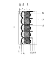
- FIG. 3 is a partial cross-sectional view of the solid-state image sensor according to the first embodiment of the present invention.
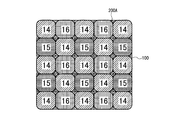
- FIG. 3 is a partial plan view of the color filter array of the solid-state image sensor according to the first embodiment of the present invention.
- It is a fragmentary sectional view of the solid-state image sensing device concerning a 2nd embodiment of the present invention.
- It is a fragmentary sectional view showing a modification of a solid-state image sensing device concerning a 2nd embodiment of the present invention.
- It is a fragmentary sectional view of the solid-state image sensing device concerning a 3rd embodiment of the present invention.
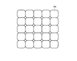
- It is a top view showing an example of 1 composition of a micro lens layer of a solid-state image sensing device concerning a 4th embodiment of the present invention.
- FIG. 6B is a process cross-sectional diagram illustrating a manufacturing process of the solid-state imaging device according to the first embodiment of the present invention, and is a diagram illustrating a partition wall structure forming process.
- FIG. 3C is a process cross-sectional diagram illustrating a manufacturing process of the solid-state imaging device according to the first embodiment of the present invention, and a diagram illustrating a first color filter forming process.
- FIG. 6C is a process cross-sectional diagram illustrating a manufacturing process of the solid-state imaging device according to the first embodiment of the present invention, and a diagram illustrating a second color filter forming process.
- FIG. 6B is a process cross-sectional diagram illustrating the manufacturing process of the solid-state imaging device according to the first embodiment of the present invention, and a diagram illustrating a third color filter forming process.
- FIG. 3C is a process cross-sectional diagram illustrating a manufacturing process of the solid-state imaging device according to the first embodiment of the present invention, and a diagram illustrating a microlens forming process.
- 6B is a process cross-sectional diagram illustrating a manufacturing process of the solid-state imaging device according to the first embodiment of the present invention, which is a diagram illustrating a microlens planarization layer forming process. It is a manufacturing process sectional view of the solid-state image sensor concerning Example 2 of the present invention, and is a figure showing a microlens formation process from a color filter layer flattening layer. It is a manufacturing process sectional view of a solid-state image sensor concerning Example 3 of the present invention, and is a figure showing a micro lens formation process. It is a manufacturing process sectional view of a solid-state image sensor concerning Example 4 of the present invention, and is a figure showing a micro lens formation process.
- the present invention describes a structure in which there is an element isolation structure between photoelectric conversion elements of a solid-state image sensor, and a partition structure is provided between each color filter. It can also be used when forming.
- the solid-state imaging device 1 includes a semiconductor substrate 10, a plurality of microlenses 200 arranged above the semiconductor substrate 10, and between the semiconductor substrate 10 and the microlens 200.
- the color filter 100 and the partition wall 50 are provided.
- a microlens planarization layer 300 is formed on the microlens 200.
- the semiconductor substrate 10 is two-dimensionally, that is, a plurality of photoelectric conversion elements 11 arranged in a matrix in a plan view and the elements separated between the photoelectric conversion elements 11 so that electrons converted between the photoelectric conversion elements 11 are not mixed.
- structure 12 The semiconductor substrate 10 is two-dimensionally, that is, a plurality of photoelectric conversion elements 11 arranged in a matrix in a plan view and the elements separated between the photoelectric conversion elements 11 so that electrons converted between the photoelectric conversion elements 11 are not mixed.
- structure 12 is two-dimensionally, that is, a plurality of photoelectric conversion elements 11 arranged in a matrix in a plan view and the elements separated between the photoelectric conversion elements 11 so
- the microlens 200 is formed of a plurality of microlens layers. Specifically, the microlens 200 is provided closest to the photoelectric conversion element 11 (that is, the first microlens layer 20 provided at the bottom and the second microlens formed above the first microlens layer 20). It is composed of layer 21.
- the color filter 100 is composed of color filters of a plurality of colors. Specifically, the color filter 100 is configured by arranging the first color filter 14, the second color filter 15, and the third color filter 16 in a predetermined regular pattern.
- the partition wall 50 is formed between each of the first color filter 14, the second color filter 15, and the third color filter 16.
- the partition wall 50 is formed of two layers, that is, an inner partition wall 30 and a partition wall 31 that covers and covers the partition wall 30.
- FIG. 1 illustrates a configuration in which the microlens flattening layer 300 exists above the microlens 200, it may be omitted depending on the configuration of the solid-state imaging device 1.
- the partition wall 50 has a two-layer structure of the partition wall 30 and the partition wall 31, it may have a one-layer structure or a two-layer structure or more depending on the structure of the solid-state imaging device 1.
- the height of the partition wall 50 may be lower or higher than that of the color filter 100. If the pixel size of the solid-state image sensor 1 is large, the partition wall 50 may be omitted.
- a color filter which is first formed in the manufacturing process of the color filter 100 and has the largest occupied area in the color filter 100 is defined as the first color filter 14.
- the color filter formed second in the manufacturing process of the color filter 100 is defined as the second color filter 15
- the color filter formed third in the manufacturing process of the color filter 100 is defined as the third color filter 16.
- the first color filter 14 is green, but the first color filter 14 may be blue or red.
- a plurality of photoelectric conversion devices 11 are two-dimensionally arranged corresponding to pixel positions.
- Each of the photoelectric conversion elements 11 has a function of converting light into an electric signal.
- each of the plurality of photoelectric conversion elements 11 receives light into an adjacent photoelectric conversion element 11 before being absorbed by the photoelectric conversion element 11 or a circuit of another photoelectric conversion element 11 in which photoelectrically converted electrons are adjacent to each other.
- the element isolation structure 12 is formed so as not to flow.
- Various methods can be used for element isolation, such as doping the semiconductor substrate 10 in the element isolation region, forming a void, or embedding a metal, an oxide, a nitride, a dielectric, or the like.
- a structure in which electrons and electrons are less likely to flow in the circuit of another photoelectric conversion element 11 adjacent thereto is desirable.
- the semiconductor substrate 10 between the photoelectric conversion elements 11 is dug by etching and then formed by depositing a metal, an oxide, a dielectric or the like.
- the semiconductor substrate 10 on which the photoelectric conversion element 11 is formed usually has a protective film formed on the outermost surface for the purpose of protecting and flattening the surface (light incident surface).
- the semiconductor substrate 10 is formed of a material that transmits visible light and can withstand a temperature of at least about 300° C.
- examples of the heat-resistant material used for the semiconductor substrate 10 include Si, oxides such as SiO 2 and nitrides such as SiN, and materials containing Si such as a mixture thereof.
- the photoelectric conversion element 11 is arranged at a position where the incident light can be received according to the material and height of the microlens 200 described later.
- the first color filter 14, the second color filter 15, and the third color filter 16 (an example of the first, second, and third color filters) that configure the color filter 100 with a predetermined pattern It is a filter corresponding to each color (green, blue and red) to be color separated.
- the first color filter 14, the second color filter 15, and the third color filter 16 are provided between the semiconductor substrate 10 and the microlens 200, and are arranged between the plurality of photoelectric conversion elements 11. In order to correspond to each of them, they are arranged in a regular pattern preset according to the pixel position.
- FIG. 2 is a plan view showing the arrangement of the first color filter 14, the second color filter 15, the third color filter 16, and the partition wall 50 formed between the color filters constituting the color filter 100. It is a figure.
- the array shown in FIG. 2 is a so-called Bayer array, and is an array in which the first color filter 14, the second color filter 15, and the third color filter 16 are spread.
- the color filters (the first color filter 14, the second color filter 15, and the third color filter 16) of the solid-state image sensor 1 are not necessarily limited to the Bayer array, and the color of each color filter is red ( It is not limited to the three colors of R), green (G), and blue (B).
- a transparent layer having a controlled refractive index or a layer that blocks visible light and transmits infrared light may be arranged in a part of the arrangement of the color filter 100.
- four adjacent pixels may have the same color, and a plurality of pixels may be arranged so as to form a Bayer array with 16 pixels.
- Each color filter that constitutes the color filter 100 contains a pigment (colorant) of a predetermined color and a thermosetting component or a photocuring component.
- the first color filter 14 contains a green pigment as a colorant
- the second color filter 15 contains a blue pigment
- the third color filter 16 contains a red pigment.
- the partition wall 50 is formed between each of the color filters of the plurality of colors (the first color filter 14, the second color filter 15, and the third color filter 16) that form the color filter 100.
- the first color filter 14, the second color filter 15, and the third color filter 16 are respectively provided by the partition wall 50 provided on the side wall portion (outer periphery) of the first color filter 14. Can be separated.
- the partition 50 has a two-layer structure in which the partition 30 is formed inside as shown in FIG. 1 and the partition 31 is formed so as to cover the outside and the semiconductor substrate 10.
- the inner partition wall 30 has a high light-shielding property and is preferably formed of, for example, a film of tungsten (W), aluminum (Al), or copper (Cu) as a metal material that can be finely processed by etching or the like with high precision. Furthermore, a laminated structure of a plurality of metal films may be used such that the lower layer is made of tungsten and the upper layer is made of titanium. Further, a compound may be used instead of a simple substance of these metals.
- the partition wall 31 covers the outside of the partition wall 30 and can guide light like an optical waveguide by using a material having a lower refractive index than the color filter, using an oxide or a nitride such as SiO 2 , SiN, or SiON. It is formed by the composition. Further, the partition wall 31 serves as a protective film for the partition wall 30, and when a metal is used for the partition wall 30, the reaction of the metal can be suppressed.
- the partition wall 30 inside the partition wall may be formed using a plurality of materials such as metal, oxide, and nitride. It is preferable to use a material having a structure that blocks or reflects light that enters an adjacent color filter and also serves as an optical waveguide.
- the height of the partition wall 50 be equal to the film thickness of each color filter that can obtain desired spectral characteristics.
- the valley portion where the film thickness of the microlens 200 described later and the partition wall 50 are arranged are likely to overlap each other in the central portion of the photoelectric conversion element 11. Therefore, the probability that light that cannot be condensed by the microlens enters from the upper portion of the partition wall 50, passes through the outer partition wall 31 and is not dispersed into the photoelectric conversion element 11 increases.
- the color filters 100 are configured to have the same film thickness but a certain width.
- the thickness is preferably about 50 nm thicker than the thickest color filter to about half the thickness of the thickest color filter.
- the thickness is preferably about 50 nm thicker than the thickest color filter to about half the thickness of the thickest color filter.
- the width of the partition wall 50 is preferably 100 nm or less, more preferably 50 nm or less.
- each color filter is formed at the place where the groove is formed on the grid.
- the color filter is made photosensitive on a flat surface and selectively exposed and developed to form a rectangular pattern.
- the film thickness of each color filter tends to be a thin film. Therefore, when forming a desired color with a thin film, it is necessary to increase the content of a coloring component such as a pigment, and as a result of the content of a photosensitive component becoming small, patterning becomes difficult.
- the microlens 200 in the solid-state imaging device 1 is arranged above the semiconductor substrate 10 at a position corresponding to a pixel position. That is, the microlens 200 is provided with a plurality of lenses at positions corresponding to the plurality of photoelectric conversion elements 11, respectively.
- the microlens 200 can compensate the decrease in the sensitivity of the photoelectric conversion element 11 by condensing the incident light incident on the microlens 200 on each of the photoelectric conversion elements 11.
- the microlens 200 of the present invention is formed of a plurality of microlens layers as shown in FIG.
- the first microlens layer 20 provided in the lower layer closest to the photoelectric conversion element 11 forms a microlens shape
- the plurality of microlens layers after the second microlens layer 21 are the first microlens layer 20.
- the structure formed on the lens surface is preferable.
- the microlens 200 is formed of two layers, the first microlens layer 20 and the second microlens layer 21.
- the first microlens layer 20 is preferably made of a high-refractive index material so that the microlens 200 can improve the light-collecting efficiency.
- the refractive index is preferably in the range of 1.75 or more and 2.15 or less.
- the refractive index of the material is 2.15 or more, the light condensing ability of the microlens 200 is improved, but the difference in the refractive index between the microlens 200 and the color filter 100 becomes large, so that the light reflected by the interface between the microlens 200 and the color filter 100 is increased. May increase and the light collection efficiency may decrease.
- an organic resin material is generally used for the microlens 200, and the organic resin has a high refractive index material of about 1.7 or less. Further, when an organic material having a high refractive index is used, the transmittance tends to decrease.
- the outside of the microlens 200 on which light is incident is in contact with air whose refractive index is close to 1.
- the refractive index of the microlens 200 is 1.75 or more, the light-collecting ability of the microlens 200 is improved, but since the refractive index difference between the microlens 200 and air is large, light is likely to be reflected. In this case, the amount of light entering the inside of the microlens 200 is reduced, which may lead to a decrease in light receiving sensitivity.
- Inorganic materials having a high refractive index and a high transmittance of visible light of 380 nm to 700 nm include silicon nitride (refractive index: about 2.0), zirconium oxide (refractive index: about 2.2), titanium oxide (refractive index: about 2.49), zinc sulfide (refractive index: about 2.35), zinc oxide (refractive index: about 2.01), hafnium oxide (refractive index: about 1.91), aluminum nitride (refractive index: about 2.1). 16), tantalum oxide (refractive index: about 2.16) and the like.
- the heat resistance of the color filter 100 provided in the lower layer is generally 300° C.
- the material for forming the microlens 200 can be formed at a temperature of 300° C. or lower, can be easily processed by a known method such as dry etching, and any material having a low extinction coefficient described later can be used. Considering the temperature and the reflection due to the difference in refractive index described above, it is preferable to use silicon nitride as the inorganic material. By using transparent and high-refractive-index silicon nitride as the inorganic material, the first microlens layer 20 becomes a high-refractive-index microlens.
- the incident light is transmitted to the pixel provided corresponding to each lens. Each can be made incident. Further, since the height of the first microlens layer 20 can be formed lower than in the conventional case, the incident light to be made incident on the adjacent pixel is blocked by the first microlens layer 20, and the solid-state imaging device 1 It is possible to suppress a decrease in the overall light receiving efficiency. Therefore, it is possible to provide the solid-state imaging device 1 exhibiting high light condensing characteristics without deteriorating the sensitivity characteristics for each color.
- the refractive index of silicon nitride is about 2.0, but the ratio of silicon and nitrogen changes depending on the film forming conditions, and the refractive index changes from about 1.7 to about 2.1. Further, when silicon nitride is used as the material of the microlens 200, the transmittance needs to be high. Since the transmittance changes depending on the film thickness of the material, it can be indicated by the extinction coefficient of the optical constant as an index. The inventors have found that the extinction coefficient is important as a material used for microlenses. The refractive index and the extinction coefficient differ depending on the film forming conditions.
- the silicon nitride used in the solid-state imaging device 1 is often formed by using CVD (Chemical Vapor Deposition).
- CVD Chemical Vapor Deposition
- the film forming conditions when forming by using CVD have different qualities depending on the control of temperature, pressure, gas species, gas flow rate and the like.
- plasma CVD Pullasma-enhanced Chemical Vapor Deposition
- a silicon nitride film suitable for the microlens 200 has a refractive index of 1.75 or more and 2.0 or less and an extinction coefficient of 1.0 ⁇ 10 ⁇ 3 in the visible light range of 380 nm or more and 700 nm or less. The following is preferable.
- a silicon nitride film suitable for the microlens 200 has a refractive index of 1.85 or more and 2.0 or less and an extinction coefficient of 1.0 ⁇ 10 ⁇ 3 or less in the wavelength range of 300 nm or more and 700 nm or less.
- the film quality is most preferable.
- silicon nitride oxide compositional formula SiON
- the silicon nitride oxide film can form a refractive index from silicon nitride (refractive index: 2.0) to silicon oxide (refractive index: 1.45) depending on the oxygen content, and the extinction coefficient can be easily controlled. Therefore, silicon nitride oxide may be used for the first microlens layer 20.
- a high-refractive first layer is formed on the color filter 100 under various film forming conditions.
- the method of forming the above-mentioned silicon nitride layer by plasma CVD is preferable.
- an intermediate sacrificial layer which is a second layer for forming a lens matrix described later, is formed.
- the intermediate sacrificial layer is formed of a resin material, and for example, a photosensitive resin having no heat flow property is used. As a result, it is possible to prevent the photosensitive resin pattern from being melted by the heat flow, and the volume of the photosensitive resin pattern from expanding to bring adjacent lenses into contact with each other.
- the photosensitive resin that does not flow heat that can be used for forming the lens matrix is a thermoplastic resin material that has a high glass transition temperature and does not lose its shape before being cured by heat treatment at 100 to 220° C. Is preferred.
- a photosensitive resin that does not flow heat contains a base resin having a mass average molecular weight (Mw: measured value by styrene conversion of gel permeation chromatography (GPC)) of 10,000 or more and 30,000 or less. Is preferred. More preferably, the mass average molecular weight is 20,000 or more and 30,000 or less.
- the mass average molecular weight of the base resin is 10,000 or more, heat resistance and heat flow resistance are improved. Further, when the mass average molecular weight of the base resin is 30,000 or less, the solubility at the time of development does not decrease, so that the generation of residues can be suppressed.
- a photosensitive photoresist is formed on the intermediate sacrificial layer to form a lens master.
- the photoresist is formed in the place where the microlens is formed, and baking is performed under the temperature condition that the shape of this photoresist is destroyed, and the resist shape is heat-flowed to form the lens shape.
- Forming a resist is performed on the entire surface of the intermediate sacrificial layer by using the lens-shaped resist as a mask, and etching is performed at a time setting such that the positive resist is completely exhausted, thereby forming a lens matrix in which the lens shape is transferred to the intermediate sacrificial layer. ..
- a lens forming method of the microlens a known method can be used in addition to the above-described method of using the resist heat flow method.
- a photomask having a gradation pattern may be used to adjust the amount of exposure to form a lens shape directly after development. Whichever method is used, since it is difficult to directly form the first microlens layer 20 in a lens shape, a sacrificial layer to be removed later is formed on the first microlens layer 20 formed flat.
- a method is suitable in which a lens shape is produced by using the lens shape, and the shape is transferred to the first microlens layer 20 by a known etching method.
- the thickness of the first microlens layer 20 in the height direction is 150 nm or more and 400 nm or less.
- the “thickness of the first microlens layer 20 in the height direction” refers to the bottom surface of the semicircular lens (the top surface of the color filter 100 in the first embodiment) to the first microlens layer 20. The height to the top of the lens.
- the pitch of each photoelectric conversion element 11 that is, the pitch of the plurality of lenses included in the first microlens layer 20
- the thickness of the first microlens layer 20 in the height direction is The film thickness may be 150 nm or more and 400 nm, and more preferably 150 nm or more and 300 nm.
- the thickness of the first microlens layer 20 in the height direction is increased, the incident light to be made incident on the adjacent pixel is blocked by the first microlens layer 20, and the solid-state imaging device 1
- the light receiving efficiency (light receiving sensitivity) of the device decreases.
- the film thickness (lens height) of the first microlens layer 20 is increased under the condition that the area where the microlens 200 is formed is small, the film thickness at the portion corresponding to the valley portion of the lens becomes thick and the lens shape collapses. There is also a problem that a region where light is mixed is formed.
- the film thickness range to the above range, these problems can be suppressed, and the solid-state imaging device 1 exhibiting high light condensing characteristics can be provided.
- the position of the light condensing point can be placed on the color filter 100, so that the sensitivity characteristic is improved.
- the height of the first microlens layer 20 in the range of 150 nm or more and 300 nm or less, good sensitivity characteristics can be obtained in all colors of green (G), blue (B), and red (R). You can
- the second microlens layer 21 of the microlens 200 is a layer that reduces reflection by the first microlens layer 20.
- the refractive index of the first microlens layer 20 is about 1.75 or more and 2.15 or less
- the air with a low refractive index is on the outside, so that the surface of the first microlens layer 20 is There is a lot of reflection and sensitivity is likely to decrease. Therefore, the second and subsequent layers of the microlens 200 including a plurality of layers are formed as antireflection layers by controlling the refractive index. That is, by providing the second microlens layer 21 on the lens surface of the first microlens layer 20, it is possible to prevent the sensitivity characteristic of the solid-state imaging device 1 from being impaired.
- the refractive index of the second microlens layer 21 is preferably lower than the refractive index of the first microlens layer 20, for example, 1.4 or more and 1.75 or less.
- the refractive index of the second microlens layer 21 is preferably lower than the refractive index of the first microlens layer 20, for example, 1.4 or more and 1.75 or less.
- the microlens 200 has a two-layer structure, and silicon oxide (SiO 2 ) or silicon oxynitride (SiON) having a large oxygen content is suitable for the second microlens layer 21. There is. That is, it is preferable that the second microlens layer 21 has a higher oxygen content than the first microlens layer 20.
- a coating type material such as SOG (Spin On Glass) or siloxane may be used instead of the vapor phase film forming method such as plasma CVD. Any known method may be used as long as it can be formed at a heat resistant temperature of 300° C. or lower of the color filter in the lower layer.
- the film thickness of the second microlens layer 21 is preferably 5 nm or more and 2000 nm or less, more preferably 10 nm or more and 200 nm or less, and further preferably 50 nm or more and 150 nm or less.
- the ratio (T2/T1) of the film thickness T2 of the second microlens layer 21 to the film thickness T1 of the first microlens layer 20 described above is preferably 0.125 or more and 1.0 or less.
- Microlens flattening layer In the present embodiment, a structure is shown in which the microlens flattening layer 300 having a flat upper surface is formed on the lens surface of the microlens 200 above the microlens 200 (light incident direction). There is.
- an air layer is provided outside the microlens 200, and a module structure such as a condenser lens and an infrared cut plate is formed on the camera module structure.
- the structure of the microlens 200 is also miniaturized, and each lens forming the microlens 200 is The distance is close to the wavelength of light. Therefore, there is a high possibility that the structure of the microlens itself has a structure that affects the incident light like a Fresnel lens or a diffractive lens. Therefore, even in the case of the general solid-state imaging device in which the air layer is normally outside as shown in the former case, it is suitable to form the microlens flattening layer 300 above the microlens 200.
- the material of the microlens flattening layer 300 may be an organic material or an inorganic material, but a material considering the refractive index is preferable.
- a material between air and the refractive index of the second microlens layer 21 on the surface of the microlenses 200 is desirable. ..
- the refractive index is preferably 1.1 or more and 1.6 or less, and more preferably 1.20 or more and 1.45 or less.
- a material having a refractive index in this range and a high transmittance for visible light is desirable.
- the film thickness is not particularly limited as long as it is 100 nm or more and 100 ⁇ m or less, but a film thickness that can flatten the microlens 200 is desirable.
- a refractive index of 1.6 or less can be formed by containing a siloxane polymer, silica, or a fluoropolymer as an inorganic polymer in an organic resin, or by containing a hollow filler. Not limited to the above method, there is no problem as long as it is a combination of materials having high transparency and flatness.
- the microlens 200 is formed on the color filter 100.
- the second microlens layer 21 is formed on the first microlens layer 20.
- the film thickness of the first microlens layer 20 (the height from the lens bottom surface to the lens apex) is 150 nm or more and 400 nm or less.
- the description is based on the configuration of only a normal photoelectric conversion element, but in recent years, the image plane phase difference autofocus (Phase Detection AF) is formed by changing a part of the structure of the photoelectric conversion element unit for focus detection.
- a part of the arrangement may change in the image sensor, or a plurality of pixels may be formed as one pixel.
- the image plane phase difference autofocus pixel has various configurations such as one pixel, two pixels, and four pixels.
- the color filter or the microlens corresponding to the photoelectric conversion element is not necessarily the photoelectric conversion element. Not a pair.
- the configuration is such that a plurality of photoelectric conversion elements has one color filter and one microlens, or a plurality of photoelectric conversion elements and color filters has one microlens.
- the partition wall 50 is formed in accordance with these configurations. Even in the case of a solid-state image pickup device in which image plane phase difference autofocus is formed as described above, the present embodiment can be applied, and the microlens in that portion is not necessarily paired with the photoelectric conversion device, and the shape is slightly different. The other parts are the same as those in the embodiment.
- a second embodiment of the present invention will be described with reference to FIG.
- a color that flattens the unevenness of the color filter 100 between the color filter 100 and the microlens 200 and relieves the stress when the microlens 200 is formed.
- the solid-state imaging device 1 according to the first embodiment is different in that the filter flattening layer 40 is formed.
- the color filter flattening layer 40 is formed on the upper surfaces of the color filters 100 and the partitions 50 formed on the semiconductor substrate 10.
- the film thickness of the color filter flattening layer 40 is formed by each color filter (first color filter 14, second color filter 15, third color filter 16) forming the color filter 100 and the partition wall 50.
- the film is formed with a film thickness that can flatten the step.
- the first microlens layer 20 is formed on the color filter flattening layer 40.
- the first microlens layer 20 is formed of an inorganic material and has a high refractive index and a high extinction coefficient. When a low microlens is formed, the microlens is likely to be formed with stress.
- the thermal expansion coefficient of the color filter 100 in the lower layer is different from that of the microlens 200 when the heating process proceeds after the baking process or the like. Problems such as misalignment may occur.
- the color filter flattening layer 40 can alleviate such a stress shift.
- the first microlens layer 20 if the film is formed under the condition that the refractive index and the extinction coefficient are important, the flatness may be poor and the film may be formed following the unevenness of the pattern. There may be a gap between the color filter 100 and the color filter 100.
- the color filter flattening layer 40 below the first microlens layer 20, the gap between the color filter flattening layer 40 and the color filter 100 is filled and the deterioration of the sensitivity characteristic is prevented. You can
- the refractive index of the microlens 200 is 1.75 or more and 2.15 or less, and the refractive index of each color filter is different for each color, but is generally 1.4 or more and 1.7 or less.
- the refractive index of the color filter flattening layer 40 is preferably 1.6 or more and 1.8 or less, and more preferably 1.6 or more and 1.7 or less.
- the material forming the color filter flattening layer 40 is a material to which stress from an organic resin or the like is unlikely to be applied, and is preferably a material which is transparent to visible light having a wavelength of 380 nm to 700 nm and has a high transmittance.
- the material of the color filter flattening layer 40 examples include acrylic resin, epoxy resin, polyimide resin, phenol novolac resin, polyester resin, urethane resin, melamine resin, urea resin, styrene resin and silicon. It is formed of a resin containing one or more of a series resin and the like. Further, the color filter flattening layer 40 is made of, for example, silicon, carbon, oxygen, hydrogen, tin, zinc, indium, aluminum, gallium, titanium, molybdenum, tungsten, niobium, tantalum, hafnium, silver, and fluorine other than organic compounds. It may be formed of a compound containing at least one kind, an oxide compound or a nitride compound.
- the color filter flattening layer 40 is formed of these materials in a single layer or a multilayer.
- the color filter flattening layer 40 may be formed by using an organic resin.
- silicon nitride oxide may be used as the material of the color filter flattening layer 40 to increase the proportion of oxygen, thereby adjusting the refractive index to form the flattening layer.
- the thickness of the color filter flattening layer 40 is preferably in the range of 10 nm or more and 300 nm or less. Further, the color filter flattening layer 40 is preferably thin from the viewpoint of miniaturization of the solid-state imaging device 2 and suppressing color mixing, and the thickness of the color filter flattening layer 40 is more preferably 10 nm or more and 150 nm or less. Further, the color filter flattening layer 40 of the present embodiment also has a purpose of relaxing the difference in stress and the coefficient of thermal expansion, and it is preferable that the color filter flattening layer 40 is a thin film within the range where this purpose can be achieved.
- the first microlens layer 20 is formed on the color filter flattening layer 40 that flattens the color filter 100 formed as described above.
- the first microlens layer 20 is formed of an inorganic material, stress is easily included under the condition that the extinction coefficient is close to 0 by increasing the refractive index. Similar to the first embodiment, when silicon nitride (SiN) is used for the first microlens layer 20, this tendency becomes remarkable.
- SiN silicon nitride
- the first microlens layer 20 is directly formed on the lower color filter 100, it is necessary to form the first microlens layer 20 with reduced stress, and the range of formation conditions tends to be narrowed. ..
- the color filter flattening layer 40 is provided below the first microlens layer 20, there is an advantage that the range of conditions for forming the first microlens can be expanded.
- the height of the first microlens layer 20 (the height from the upper surface of the color filter flattening layer 40 to the apex of the first microlens layer 20) is preferably about 150 nm to 400 nm.
- the solid-state imaging device 2 has the microlens flattening layer 300, but the configuration is not limited to this.
- the solid-state imaging device 2A of the modified example of the second embodiment includes a semiconductor substrate 10, a color filter 100, a color filter flattening layer 40, a microlens 200, and a partition wall 50. Is equipped with. That is, it is different from the solid-state imaging device 2 according to the second embodiment in that the microlens flattening layer 300 is not provided.
- the semiconductor substrate 10, the color filter 100, the color filter flattening layer 40, the microlens 200, and the partition wall 50 have the same configurations as the parts described in the first embodiment and the second embodiment, so description thereof will be omitted. To do.
- the color filter flattening layer 40 is provided between the color filter 100 and the microlens 200. Therefore, the color filter flattening layer 40 relieves stress from other layers, and the lower surface of the microlens 200 can be flattened, so that the microlens 200 can be preferably formed.
- the solid-state image sensor 2 of the present embodiment has an advantage of widening the range of conditions for forming the first microlens layer 20. Specifically, there is an advantage that the film forming temperature can be increased when using a film forming apparatus such as plasma CVD.
- Inorganic materials and the like tend to change the included stress and the like depending on the film formation temperature, so that the color filter flattening layer 40 has the effect of relaxing the stress and the like as described above. Therefore, even if the film-forming temperature fluctuates to some extent from the set temperature, there is an effect that quality problems do not occur.
- the microlens 200 has the third microlens layer 22 provided on the upper surface of the second microlens layer 21.
- the solid-state image sensor 1 according to the first embodiment is different.
- the microlens 200 has a first microlens layer 20, a second microlens layer 21, and a third microlens layer 22.
- the first microlens layer 20 and the second microlens layer 21 are the same as the first microlens layer 20 and the second microlens layer 21 of the solid-state imaging device 1 according to the first embodiment.
- the third microlens layer 22 is a layer that reduces reflection by the first microlens layer 20, and has a lower refractive index than the second microlens layer 21.
- the third microlens layer 22 preferably has a higher oxygen content than the second microlens layer 21.
- the microlens 200 has a structure of three layers, but any number of layers may be used as long as the refractive index tends to decrease from the lower layer near the photoelectric conversion element 11 to the upper layer.
- the color filter flattening layer 40 is not provided between the color filter 100 and the microlens 200, but the color filter flattening layer 40 is provided. Good.
- the steps up to the step of forming the first microlens layer 20 are the same as those in the first embodiment.
- the second microlens layer 21 is formed.
- the second microlens is formed with a refractive index in the range of 1.5 to 1.75.
- the third microlens layer 22 is formed.
- the third microlens layer 22 is formed with a refractive index of 1.3 or more and 1.5 or less. Reflection on the surface of the microlens is reduced by gradually decreasing the refractive index from the inside to the outside of the microlens to reduce the difference in the refractive index from the air.
- the second and subsequent microlenses may be formed layer by layer or continuously.
- silicon oxynitride formed by plasma CVD it is formed under the condition that the ratio of the nitride is large at the beginning, and the flow rate of the gas is changed so as to change to the condition where the amount of oxide is large,
- the refractive index may be controlled.
- the microlens planarizing layer 300 in the subsequent step can be omitted and the process can be facilitated.
- a low refractive index material having a refractive index of 1.2 or more and 1.5 or less may be used.
- FIG. 6 is a plan view showing a configuration example of the solid-state imaging device 4 according to this embodiment.
- the solid-state imaging device 4 includes at least a semiconductor substrate 10, a color filter 100, a microlens 200A, and a partition wall 50.
- the solid-state imaging device 4 is different from the solid-state imaging devices 1 to 3 of the first to third embodiments in that it includes a microlens 200A instead of the microlens 200.
- the microlens 200A will be described in detail.
- the semiconductor substrate 10, the color filter 100, the color filter flattening layer 40, and the partition wall 50 have the same configurations as the parts described in the first embodiment and the second embodiment, and therefore description thereof will be omitted.
- the microlens 200A is formed of a plurality of (for example, two layers) microlens layers.
- the microlens 200A includes the first microlens layer 20A provided in the lower layer closest to the photoelectric conversion element 11 and the second microlens layer provided on the lens surface of the first microlens layer 20A.
- the case of including the lens layer 21A will be described.
- the sectional configurations of the first microlens layer 20A and the second microlens layer 21A are the same as those of the first microlens layer 20 and the second microlens layer 21 of the microlens 200, and will be described later with reference to FIG. In, the first microlens layer 20A and the second microlens layer 21A are not shown.
- the microlens 200A has a plurality of lenses respectively corresponding to the plurality of photoelectric conversion elements 11. As shown in FIG. 6, in the microlens 200A, a plurality of adjacent lenses are in contact with each other in a plan view. In the microlens 200A, a plurality of adjacent lenses are in linear contact with each other in a plan view, but they do not necessarily have to be in linear contact. In addition, the microlens 200A has gaps on the corners of the first color filter 14, the second color filter 15, and the third color filter 16 that form the color filter 100, and the lens is The shape may not cover the corners.
- the Fill Factor indicating the ratio of the lens covering one pixel having the photoelectric conversion element 11 is preferably 80% or more and 100% or less, and 85% or more and 95% or less. Is more preferable.
- the Fill Factor is 80% or more and 100% or less, deterioration of the light-collecting characteristics due to the gap between the adjacent lenses is suppressed, and the light-receiving sensitivity is green (G), blue (B), or red (R). Is improved, and when it is 85% or more and 95% or less, the light receiving sensitivity is particularly improved, which is preferable.
- FIG. 7 is a plan view schematically showing a planar configuration of four pixels and four lenses provided on each pixel P.
- the Fill Factor is defined by the following equation (1).
- Fill Factor [%] ⁇ 1-(a ⁇ a)/(A ⁇ A) ⁇ 100 (1)
- A is the pixel size
- a is the distance on the diagonal line of the gap generated in the lens
- a ⁇ A is the ratio of the lens covering one pixel, which is 100% at the maximum.
- the microlens 200A as described above can be formed by using a method for forming a microlens via a lens matrix described later. As shown in FIG. 8, when a microlens (200′) is formed without using a lens matrix described later, a plurality of adjacent lenses of the microlens 20′ do not contact each other on each pixel P. , A plurality of lenses are formed independently of each other. In this case, the gap G between the lenses becomes large, and it is difficult to improve the light collection efficiency.
- the solid-state imaging device 4 includes the microlens 200A having a lens having a Fill Factor of preferably 80% or more and 100% or less, more preferably 85% or more and 95% or less, thereby improving the light condensing characteristics. be able to.
- the influence of the sensitivity characteristic due to the gap of the microlens 200A is influenced by lowering the lens height of the microlens 200A (first microlens layer 20). Therefore, when the film thickness of the first microlens layer 20 is 150 nm or more and 400 nm or less, by reducing the gap between the lenses, it is possible to provide a fine and highly sensitive solid-state imaging device 4.
- Example 1 In Example 1, a manufacturing method similar to that of the solid-state imaging device 1 (see FIG. 1) according to the first embodiment described above will be described.
- photoelectric conversion elements 11 arranged two-dimensionally are provided, and each photoelectric conversion element 11 is separated by an element separation structure 12.
- the semiconductor substrate 10 was prepared (FIG. 9A).
- the partition wall 50 was formed on the semiconductor substrate 10 (FIGS. 9B and 9C).
- a tungsten film was formed to a thickness of 350 nm by plasma CVD.
- a positive resist (TDMR-AR: manufactured by Tokyo Ohka Kogyo Co., Ltd.) was spin-coated on the tungsten film at a rotation speed of 1000 rpm using a spin coater, and then prebaked at 90° C. for 1 minute.
- a sample was prepared in which a photoresist, which is a photosensitive resin mask material layer (etching mask), was applied to a film thickness of 1.5 ⁇ m.
- the positive type resist which is the photosensitive resin mask material layer, is exposed to ultraviolet rays, and a portion of the ultraviolet rays irradiated causes a chemical reaction to be dissolved in a developing solution.
- Photolithography of exposing this sample through a photomask was performed.
- the exposure apparatus used was an exposure apparatus using a wavelength of i-line as a light source.
- the portion of the photosensitive resin mask material layer forming the color filter was irradiated with ultraviolet rays.
- a development step was performed using 2.38 mass% TMAH (tetramethylammonium hydride) as a developing solution to form a photosensitive resin mask layer having an opening at a position where a color filter is formed.
- TMAH tetramethylammonium hydride
- dehydration baking is often performed after development to cure the photoresist, which is the photosensitive resin mask material layer. This time, dehydration baking was performed at a temperature of 120°C.
- the photosensitive resin mask layer was formed to have a film thickness of 1.5 ⁇ m.
- dry etching was performed using the photosensitive resin mask layer as a mask.
- the dry etching apparatus used was a parallel plate type dry etching apparatus. Further, the etching conditions were changed in the middle so that the underlying semiconductor substrate 10 was not affected, and the dry etching was performed in multiple stages.
- etching was carried out using an etching gas in which SF 6 and Ar gas were mixed.
- the gas flow rate of SF 6 was 50 ml/min, and the gas flow rate of Ar was 100 ml/min.
- the pressure inside the chamber at this time was set to 2 Pa and the RF power was set to 1000 W. Under this condition, about 180 nm, which is 90% of the total film thickness of 200 nm of the tungsten film exposed from the photosensitive resin mask layer, was etched.
- the etching conditions were changed to the following.
- etching was performed using an etching gas in which three kinds of SF 6 , O 2 , and Ar gas were mixed.
- the gas flow rate of SF 6 was 5 ml/min, the gas flow rate of O 2 was 50 ml/min, the gas flow rate of Ar was 100 ml/min, and all the tungsten film exposed from the photosensitive resin mask layer was removed by etching.
- the photosensitive resin mask layer used as the etching mask was removed.
- the method used at this time was a method using a solvent, and the photosensitive resin mask layer was removed with a spray cleaning device using a stripping solution 104 (manufactured by Tokyo Ohka Kogyo Co., Ltd.). After that, ashing with oxygen plasma was performed to remove the remaining photosensitive resin mask layer.
- the inner partition walls 30 having a tungsten partition structure in a lattice shape were formed on the semiconductor substrate to have a film thickness (height) of 350 nm and a width of 60 nm (FIG. 9B).
- the SiO 2 film to be the partition wall 31 was formed by using plasma CVD.
- the SiO 2 film forming conditions used at this time are the conditions for forming a thick film in the height direction with respect to the tungsten pattern (partition wall 30 ).
- the height of the partition wall 50 formed by the partition wall 30 and the partition wall 31 was 600 nm (FIG. 9C).
- a resist containing a green (G) pigment and having photosensitivity (hereinafter referred to as a green resist 14a) was applied to the entire surface of the semiconductor substrate 10 (FIG. 10A).
- HMDS treatment hydrophobic surface treatment
- the green resist 14a was selectively exposed by photolithography and then developed to form a green filter having a pattern corresponding to the formation position of the first color filter 14.
- an acrylic resin having photosensitivity was used as the resin as the main component of the green resist 14a.
- the pigments used for the green resist 14a are C.I. I. PG58, C.I. I. It was PY150 and the pigment concentration was 60 mass %.
- the film thickness of the green filter was 600 nm.
- the first color filter 14 was formed by baking at 230° C. for 6 minutes on a hot plate to cure it (FIG. 10( b )). After passing through this heating step, peeling of the first color filter 14 and collapse of the pattern were not confirmed even after passing through steps such as the third color filter forming step.
- a second color filter forming step of forming the second color filter 15 was performed (FIGS. 11A and 11B).
- a photosensitive resist containing a blue (B) pigment (hereinafter referred to as “blue resist”) is provided on the entire surface of the semiconductor substrate 10 except the first color filter 14 forming region. It was applied (FIG. 11(a)).
- the entire surface of the semiconductor substrate 10 may be subjected to a hydrophobic surface treatment (HMDS treatment) in order to improve adhesion.
- HMDS treatment hydrophobic surface treatment
- the blue resist was selectively exposed by photolithography and then developed to form a blue filter pattern corresponding to the position where the second color filter 15 was formed.
- an acrylic resin having photosensitivity was used as a resin as a main component of the blue resist.
- the pigments used for the blue resist are C.I. I. PB156, C.I. I. PV23 and the pigment concentration was 50 mass %.
- the film thickness of the blue filter was 590 nm.
- a third color filter forming step of forming the third color filter 16 was performed (FIGS. 12A and 12B ).
- a resist containing a red (R) pigment and having photosensitivity hereinafter, referred to as a red resist
- HMDS treatment hydrophobic surface treatment
- red filter pattern corresponding to the formation position of the third color filter 16.
- a photosensitive acrylic resin was used as the resin as the main component of the red resist.
- the pigment used for the red resist is C.I. I. PR254, C.I. I. It was PY139 and the pigment concentration was 60 mass %.
- the film thickness of the red filter was 610 nm.
- a microlens forming step of forming the microlens 200 was performed (FIGS. 13A to 13E).
- a silicon nitride (SiN) film 20a having a film thickness of 600 nm was formed on the formed color filter 100 using plasma CVD (FIG. 13A).
- the film formation temperature in plasma CVD was 240° C.
- the formed silicon nitride film 20a had a refractive index of 1.85 and an extinction coefficient of 1.0 ⁇ 10 ⁇ 3 or less after a wavelength of 340 nm. Further, the extinction coefficient of the silicon nitride film 20a at a wavelength of 330 nm was 4.0 ⁇ 10 ⁇ 2 , and it was confirmed that light was somewhat absorbed in this region.
- a resin having alkali solubility, photosensitivity, and thermal reflow property was applied onto the formed silicon nitride film 20a to form a photosensitive sacrificial layer.
- the photosensitive sacrificial layer was patterned by a photolithography process using a photomask, and then heat-treated at 200° C. to form a lens matrix 20b as a sacrificial layer.
- the lens matrix 20b was formed by providing a plurality of smooth semicircular shapes each having a thickness of about 300 nm (FIG. 13B).
- the patterns of the lens mother die 20b is transferred to the silicon nitride film 20a, the first micro-lens layer 20 Formed (FIG. 13( c )).
- the etching rate at this time was such that the lens matrix 20b and the silicon nitride film 20a have the same etching rate and the selection ratio is 1.
- the dry etching time was 5 minutes. Thereby, the height from the apex of the semicircular lens of the first microlens layer 20 to the bottom surface of the semicircular lens (the upper surface of the red third color filter 16) is 300 nm.
- the microlens layer 20 was formed.
- a silicon oxide (SiO 2 ) film to be the second microlens layer 21 was formed with a thickness of 50 nm by using plasma CVD as a film forming device (FIG. 13). (D)).
- the refractive index of the silicon oxide film was 1.45. Thereby, the microlens 200 was formed.
- microlens flattening layer forming step of forming the microlens flattening layer 300 was performed (FIG. 14).
- the microlens flattening layer 300 is formed using, for example, an organic resin having a refractive index of 1.35. This organic resin was spin-coated by a spin coating method to a film thickness of 500 nm to flatten the microlens 200. Note that the microlens flattening layer 300 is not limited to this thickness, and may be thicker than the height of the unevenness of the microlens 200 and have a thickness capable of flattening the unevenness.
- the solid-state imaging device 1 of the example was formed by the above steps.
- the microlens 200 is formed of a material having a high refractive index, so that the light-collecting ability is improved, and the extinction coefficient is small, so that the light transmission of the material
- the characteristics are high, and by forming the film thickness of the microlens 200 to 300 nm, good sensitivity can be obtained with all three color filters of red, blue and green.
- the second embodiment is different from the first embodiment in that the color filter flattening layer 40 is provided between the color filter 100 and the microlens 200.
- each process up to forming the color filter 100 is the same as each process up to forming the color filter 100 described in the first embodiment (FIGS. 9A to 12B). .. Therefore, the configuration after the color filter 100 is formed will be described below.
- the color filter flattening layer 40 is formed on the upper surface of the color filter 100 (FIG. 15A).
- the color filter flattening layer 40 is provided to reduce unevenness due to a difference in height between the color filter 100 formed of three colors of red, blue, and green and the partition wall 50, and of the microlens 200 formed above the color filter 100. It is formed to relieve stress.
- the microlens 200 is formed of silicon nitride, the coefficient of thermal expansion of the microlens 200 is different from that of the color filter 100, but the color filter flattening layer 40 is provided to reduce the difference in coefficient of thermal expansion. There is also an effect.
- the viscosity of a coating liquid containing an acrylic resin was adjusted, spin coating was performed at a rotation speed of 1000 rpm, and heat treatment was performed on a hot plate at a temperature of 230° C. for 6 minutes to cure the resin and flatten the color filter.
- Layer 40 was formed. At this time, the film thickness of the color filter flattening layer 40 was 100 nm, and the visible light transmittance of the color filter flattening layer 40 was 99%.
- the refractive index of the color filter flattening layer 40 was 1.6.
- the steps of forming the first microlens layer 20 are the same as the steps of forming the first microlens layer 20 of Example 1 (FIGS. 13A to 13C). )) is the same. Further, the steps after the step of forming the second microlens layer 21 are the same as the steps after the step of forming the second microlens layer 21 of Example 1 (FIGS. 13D and 14).
- the solid-state imaging device of Example 2 was formed by the above steps. In Example 2, by forming the color filter flattening layer 40 under the first microlens layer 20, the stress can be eased easily, and the first microlens can be used in a large sample range such as a 300 mm wafer surface. There is an advantage that the conditions for forming the layer 20 are widened.
- Example 3 is different from Example 1 in that the number of layers of microlenses to be laminated when forming the microlens 200 is three.
- the steps up to the formation of the first microlens layer 20 are the same as the steps up to the formation of the first microlens layer 20 in the first embodiment (FIGS. 9A to 13C). )) is the same. Therefore, the configuration after forming the first microlens layer 20 will be described below.
- a silicon nitride oxide (SiON) film to be the second microlens layer 21 was formed by using plasma CVD as a film forming device.
- SiH 4 , NH 3 , and N 2 are used as gas species when forming a silicon nitride (SiN) film, but N 2 O gas is also added when forming a silicon nitride oxide (SiON) film.
- the refractive index of the silicon nitride oxide (SiON) film is controlled mainly by changing the flow rate ratio of the N 2 O gas and the other gas.
- a silicon nitride oxide (SiON) film having a refractive index of 1.68 is formed with a thickness of 50 nm.
- a silicon oxide (SiO 2 ) film was formed as a third microlens layer 22 on the second microlens layer 21 by using plasma CVD (FIG. 16A).
- the silicon oxide (SiO 2 ) film has a refractive index of 1.47 and a film thickness of 50 nm.
- microlens flattening layer 300 was formed in the same manner as microlens flattening layer 300 of Example 1 (FIG. 14) (FIG. 16B). Thereby, the microlens 200 was formed.
- the solid-state imaging device of Example 3 was formed by the above steps. In this embodiment, by forming the microlens 200 in multiple layers, there is an advantage that the reflectance of the microlens 200 itself formed of a high refractive index material is reduced and the light receiving sensitivity is improved.
- Example 4 when forming the microlens 200, a lens matrix 20e made of a resin material is formed on the silicon nitride film 20a to be the first microlens layer 20, and a plurality of lenses are in contact with each other.
- This example differs from Example 1 in that the first microlens layer 20 was formed using the matrix 20e as a mask and that the microlens planarizing layer 300 was not formed.
- each step up to forming the first color filter 14, the second color filter 15 and the third color filter 16 is the same as in the first embodiment (FIGS. 9A to 12B). It is similar to FIG. Therefore, hereinafter, the formation of the silicon nitride film 20a to be the first microlens layer 20 and the subsequent steps will be described.
- an intermediate sacrificial layer 20c was formed on the silicon nitride film 20a with a resin material.
- a mask 20d having a lens shape was formed of a resist on the intermediate sacrificial layer 20c.
- the intermediate sacrificial layer 20c was processed into a microlens shape by dry etching using the mask 20d as a mask to form a lens matrix 20e. At this time, the microlens shape was transferred to the intermediate sacrificial layer 20c so that the distance between the lenses was narrowed.
- the silicon nitride film 20a was processed into a microlens shape by dry etching using the intermediate sacrificial layer 20c (lens matrix 20e) processed into a microlens shape as a mask. Thereby, the first microlens layer 20 was formed.
- the second microlens layer 21 was formed, and the microlens 200 was formed. At this time, the microlens 200 was formed so that the Fill Factor was 90%.
- a solid-state image sensor having the lens 200 was formed.
- the height of the first microlens can be made variable by changing the height of the lens matrix for dry etching when forming the solid-state imaging device of each of the above-described embodiments.
- the Fill Factor of the microlens layer can be made variable by changing the shape of the lens matrix. Therefore, the height of the microlens and the Fill Factor were changed at the levels shown in Table 1 to evaluate the light receiving sensitivity. Further, as a comparison, a comparison was made with the following conventional structure in which a high-refractive index material is not applied to a microlens and a microlens is formed using an organic resin which is a conventional material.
- sample No. 1 to sample No. Reference numeral 5 is a solid-state image sensor having a conventional structure
- sample No. 14 is a solid-state imaging device having a structure according to the third embodiment
- sample No. Sample Nos. 15 to 19 are solid-state image pickup devices having the structure according to the fourth embodiment.
- the solid-state image pickup device having the conventional structure is different from the solid-state image pickup device of each embodiment in that the microlenses are formed of an organic resin material containing an acrylic resin.
- the microlens in the solid-state image sensor having the conventional structure was formed as follows. The microlens in the solid-state imaging device having the conventional structure was formed by the same process as in Example 1 (FIGS. 9A to 12B) up to the color filter forming process. Next, an organic resin material containing an acrylic resin was spin-coated to a thickness of 1.0 ⁇ m and cured by heating at 230° C. to form an organic resin film.
- a resin having alkali solubility, photosensitivity, and thermal reflow property was applied on the formed organic resin film to form a photosensitive sacrificial layer.
- the photosensitive sacrificial layer was patterned by a photolithography process using a photomask and then heat-treated at 200° C. to form a lens matrix.
- Sample No. 1 to sample No. In No. 5 a lens master block having a plurality of smooth semicircular shapes each having a thickness of about 150 nm to about 500 nm was formed.
- sample No. 1 to sample No. 19 shows the microlens material and structure of each solid-state imaging device of 19.
- sample No. 1 to sample No. 19 The result of having compared the light receiving sensitivity evaluation result of each 19 solid-state image sensor is shown.
- Sample No. 1 to sample No. The light-receiving sensitivity of each solid-state imaging device of No. 19 indicates the amount of increase or decrease of the light-receiving sensitivity when the light-receiving sensitivity of the solid-state imaging device of the conventional structure (Sample No. 1) having a microlens height of 200 nm is used as a reference.
- Sample No. 1 to sample No. From the result of No. 5, it was found that in the conventional structure, as the height of the microlens is increased, the light receiving sensitivity is improved in many colors. However, a microlens having a height of more than 550 nm cannot be manufactured because it is difficult to form due to the process. In addition, sample No. In the solid-state image sensor 5 (microlens height 550 nm), the lens shape was not hemispherical but the lens shape was broken, and the light receiving sensitivity was lowered. If the microlenses are further miniaturized than the solid-state imaging device formed this time, it becomes more difficult to form a shape having a high lens height.
- the green light receiving sensitivity is high when the microlens height is 120 nm, and the conventional structure (Sample No.) is used when the microlens height is 150 nm to 500 nm.
- the result is that the light receiving sensitivity is higher than that in the case of 1).
- the height of the microlens was 550 nm, the light receiving sensitivity was lower than that of the conventional structure (Sample No. 1).
- the refractive index of the microlens is increased, the light that should enter the adjacent pixels may be blocked by the lens, and the light receiving sensitivity may not be improved in all color filters. Was shown.
- sample No. 1 having the same microlens height. 9 sample No. 13, sample No. As a result of comparing No. 14, sample No. 14 having the configuration according to the first and third embodiments. 13, No. It was found that particularly high light receiving sensitivity was obtained in No. 14.
- the color filter flattening layer 40 having different refractive index is provided between the color filter 100 and the microlens 200, the sample No. 13, No. It is considered that the reflection of light occurs and the light-receiving sensitivity is partially reduced as compared with Example 14 (Examples 1 and 3).
- the color filter flattening layer 40 was formed to have a film thickness of 100 nm.
- Sample No. 9 The light receiving sensitivity of Sample No. 9 is Sample No. Although it is lower than the light receiving sensitivity of No. 13, there is an advantage that manufacturing is easy because the range of forming conditions is wide in the manufacturing process.
- Sample No. in Example 14 Example 3
- the microlenses were formed in a three-layer structure, the effect of reducing light reflection on the surface of the microlenses having a high refractive index was obtained.
- the light receiving sensitivity is higher than that in Example 13 (Example 1).
- a solid-state imaging device having a plurality of adjacent lenses in contact with each other and having a micro lens 200 having a Fill Factor of 80% or more and 100% or less. Further, it is preferable to use a solid-state image sensor having a plurality of adjacent lenses in contact with each other, having a gap on each corner of each color filter, and having a micro lens 200 having a Fill Factor of 85% or more and 95% or less. preferable.
- the color filter 100 is formed by applying a color filter material having photosensitivity to the entire surface, and selectively exposing a portion where the color filter is formed to be cured to obtain a color filter.
- a filter pattern was formed.
- the color filter material is not limited to such a structure. For example, as shown in FIG. 19, after the color filter material is not photosensitized and is cured by heat baking using a thermosetting resin or the like, a mask pattern is formed with a photoresist and an opening is desired. It is also possible to use a process of etching away only the color filter of. Further, this dry etching process and a lithography process using a photosensitive color filter may be used together.
- any of the embodiments may be used as the color filter forming step.
- the partition wall 50 is formed to have the same height as the color filter 100 will be described, a partition wall structure having a height about half that of the color filter may be used.
Landscapes
- Physics & Mathematics (AREA)
- General Physics & Mathematics (AREA)
- Optics & Photonics (AREA)
- Solid State Image Pick-Up Elements (AREA)
Abstract
微細画素でも集光効率を向上させ、全ての色で高精細で感度の良い固体撮像素子及び固体撮像素子製造方法を得る。固体撮像素子は、半導体基板と、半導体基板に設けられ、平面視でマトリクス状に配置された複数の光電変換素子と、複数の光電変換素子のそれぞれに対応させて配置された複数色の色フィルターが、予め設定した規則パターンで二次元的に配置された色フィルター層と、複数色の色フィルター及び複数の光電変換素子にそれぞれ対応させて配置された複数のレンズを有するマイクロレンズ層が複数積層して形成されたマイクロレンズと、を備える。複数のマイクロレンズ層のうち、光電変換素子に最も近接して配置された第1のマイクロレンズ層の膜厚は、150nm以上400nm以下である。
Description
本発明は、固体撮像素子及び固体撮像素子の製造方法に関する。
近年、デジタルカメラ等に搭載されるCCD(Charge Coupled Device)イメージセンサやCMOS(Complementary Metal-Oxide-Semiconductor)イメージセンサ等の固体撮像素子は、高画素化、微細化が進んでおり、特に微細なものでは1.1μm×1.1μmを下回る画素サイズとなっている。
固体撮像素子は、複数の光電変換素子と対になる色フィルターをそれぞれ設けることでカラー化を図っている。また、固体撮像素子に設けられた光電変換素子が光電変換に寄与する領域(開口部)は、固体撮像素子のサイズや画素数に依存する。その開口部は、固体撮像素子の全面積に対し、20%以上50%以下程度に限られている。開口部が小さいことは、そのまま光電変換素子の感度低下につながることから、固体撮像素子では感度低下を補うために光電変換素子上に集光用のマイクロレンズを形成することが一般的である。マイクロレンズで光を集光して光電変換素子の受光部に導くことで、受光部の見かけ上の開口率を大きくする事が可能になり、固体撮像素子の感度が向上できる。
また、近年、微細画素の感度やシェーディング特性を改善するために、裏面照射型固体撮像素子(BSI:Back Side Illumination)が開発されている。裏面照射型固体撮像素子では、光の入射側に多層メタル配線を設けないことで、開口部を固体撮像素子の全面積の50%以上にすることができ、入射光を効率良く光電変換素子に取り込むことができる。しかしながら、裏面照射技術を用いることで、光電変換素子が固体撮像素子の光が入射する表面側に存在する。このため、色フィルターに隣接する別の色フィルターの漏れ光が光電変換素子に入ることや、光電変換素子の内部で吸収される光が隣接する光電変換素子に入ることや、光電変換されて発生した電子が隣接する光電変換素子の回路部に流れるなどの要因で混色が発生しやすくなる。その対策として、色フィルター間に隔壁を形成し、隔壁により光を遮る、または隔壁が導波路として光を誘導するようにしている、また、光電変換素子間にも深い素子分離構造を形成し、電子の流れや光電変換素子内部で吸収される光を分離するようにしている(特許文献1、2)。
固体撮像素子の高画素化、微細化に伴い、光電変換素子と一対でマイクロレンズを形成する必要がある。このため、マイクロレンズの形成領域のサイズは小さくなり、マイクロレンズの微細化が求められている。また、マイクロレンズをそのまま微細化した場合、マイクロレンズによる集光点がずれることや、マイクロレンズの端で光の集光力が劣る。このため、各色フィルター間の隔壁部分に光が当たるなど、光を効率的に光電変換素子に集められないという問題がある。これを解決するために、マイクロレンズを微細化した上で、マイクロレンズのアスペクト比を上げる必要があるが、微細化しつつアスペクト比が高い形状に制御することは、製造プロセス上困難である。更に、アスペクト比を高くすると、隣接するマイクロレンズ同士が干渉するため、レンズ形状を維持しつつ微細化することができないという問題がある。
このような問題を解決するために、マイクロレンズの材料に屈折率の高い材料を用いて、マイクロレンズ間の平らになるスペースを設けずにマイクロレンズを形成することで、高画素化、微細化した固体撮像素子でも光の取り込み効率を向上させることが開示されている(特許文献3)。
また、マイクロレンズを複数層構造で形成し、各層の膜厚を調整することで、感度むらを抑制したマイクロレンズが開示されている(特許文献4)。さらに、特許文献5では、無機材料からなるマイクロレンズの屈折率と、マイクロレンズと色フィルターとの間に形成した非平坦化層の膜厚の関係を示して、感度特性の低減を抑制する技術が開示されている(特許文献5)。
また、マイクロレンズを複数層構造で形成し、各層の膜厚を調整することで、感度むらを抑制したマイクロレンズが開示されている(特許文献4)。さらに、特許文献5では、無機材料からなるマイクロレンズの屈折率と、マイクロレンズと色フィルターとの間に形成した非平坦化層の膜厚の関係を示して、感度特性の低減を抑制する技術が開示されている(特許文献5)。
しかしながら、マイクロレンズに屈折率の高い無機材料を用いると、画素サイズが微細化した場合、全ての色フィルターで高感度化できない場合がある。例えば、マイクロレンズの高さが高い場合、隣接する画素に入射されるべき入射光がマイクロレンズによって遮断され、受光効率が低下する場合がある。
本発明は、上述のような点に鑑みてなされたものであって、微細画素でも集光効率を向上させ、全ての色で高精細で感度の良い固体撮像素子及び固体撮像素子製造方法を提供することを目的とする。
本発明の一態様による固体撮像素子は、半導体基板と、半導体基板に設けられ、平面視でマトリクス状に配置された複数の光電変換素子と、複数の光電変換素子のそれぞれに対応させて配置された複数色の色フィルターが、予め設定した規則パターンで二次元的に配置された色フィルター層と、複数色の色フィルター及び複数の光電変換素子にそれぞれ対応させて配置された複数のレンズを有するマイクロレンズ層と、を備え、マイクロレンズ層は、光電変換素子側に最も近接して配置された第1のマイクロレンズ層と、第1のマイクロレンズ層のレンズ面上に積層するように形成された第2のマイクロレンズ層とを有し、第1のマイクロレンズ層は、膜厚が150nm以上400nm以下であり、屈折率が1.75以上2.15以下であり、かつ窒化シリコンまたは窒化酸化シリコンで形成されており、第2のマイクロレンズ層は、第1のマイクロレンズ層よりも低い屈折率を有する窒化酸化シリコンまたは酸化シリコンで形成されていることを特徴とする。
本発明の一態様による固体撮像素子の製造方法は、複数の光電変換素子が平面視でマトリクス状に配置され、複数の光電変換素子の間に素子分離構造が設けられた半導体基板上の光電変換素子を取り囲む位置に、隔壁を形成する工程と、隔壁で囲まれた光電変換素子に対応する位置に、複数色の色フィルターをそれぞれ形成する工程と、色フィルター及び隔壁の上部に、膜厚が150nm以上400nm以下である、屈折率が1.75以上2.15以下の窒化シリコン膜または窒化酸化シリコン膜を形成し、複数の光電変換素子にそれぞれ対応する位置に複数のレンズを形成して第1のマイクロレンズ層を形成する工程と、第1のマイクロレンズ層のレンズ面上に、第1のマイクロレンズ層よりも低い屈折率を有する窒化酸化シリコン膜または酸化シリコン膜を形成して第2のマイクロレンズ層を形成する工程と、を備えることを特徴とする。
本発明によれば、微細画素でも集光効率を向上させ、全ての色で高精細で感度の良い固体撮像素子及び固体撮像素子製造方法を提供することができる。
以下、本発明の実施形態について図面を参照しながら説明する。ここで、図面は模式的なものであり、色フィルター等の各層の厚みと平面寸法との関係、各層の厚みの比率等は現実のものとは異なる。また、固体撮像素子の色フィルター部の構成を示す断面図では、後述する公知のベイヤー配列を元に記載するが、実際のベイヤー配列では、3色以上の色フィルターが図面のように横に並ぶ構造とはならないが、説明の為に並べた図面で記載する。以下に示す各実施形態は、本発明の技術的思想を具体化するための構成を例示するものであって、本発明の技術的思想は、構成部品の材質、形状、構造等が下記のものに特定されるものでない。本発明の技術的思想は、特許請求の範囲に記載された請求項が規定する技術的範囲内において、種々の変更を加えることができる。
また本発明では、固体撮像素子の光電変換素子の間に素子分離構造があり、各色フィルターの間に隔壁構造がある構造について記載するが、これらの構造が無い公知の構造に対して、マイクロレンズを形成する際にも用いることができる。
1.第1の実施形態
(固体撮像素子の構成)
本発明の第1の実施形態に係る固体撮像素子の構成について、図1及び図2を用いて説明する。
図1に示すように、本実施形態に係る固体撮像素子1は、半導体基板10と、半導体基板10の上方に配置された複数のマイクロレンズ200と、半導体基板10とマイクロレンズ200との間に設けられた色フィルター100及び隔壁50とを備えている。また、マイクロレンズ200の上には、マイクロレンズ平坦化層300が形成されている。
半導体基板10は、二次元的、すなわち平面視でマトリクス状に配置された複数の光電変換素子11と、各光電変換素子11間で変換した電子が混在しないように光電変換素子11間に素子分離構造12とを有している。
(固体撮像素子の構成)
本発明の第1の実施形態に係る固体撮像素子の構成について、図1及び図2を用いて説明する。
図1に示すように、本実施形態に係る固体撮像素子1は、半導体基板10と、半導体基板10の上方に配置された複数のマイクロレンズ200と、半導体基板10とマイクロレンズ200との間に設けられた色フィルター100及び隔壁50とを備えている。また、マイクロレンズ200の上には、マイクロレンズ平坦化層300が形成されている。
半導体基板10は、二次元的、すなわち平面視でマトリクス状に配置された複数の光電変換素子11と、各光電変換素子11間で変換した電子が混在しないように光電変換素子11間に素子分離構造12とを有している。
マイクロレンズ200は、複数のマイクロレンズ層で形成されている。具体的には、マイクロレンズ200は、光電変換素子11に最も近接して設けられた(すなわち、最も下部に設けられた第1のマイクロレンズ層20、その上部に形成された第2のマイクロレンズ層21で構成されている。
色フィルター100は、複数色の色フィルターで構成されている。具体的には、色フィルター100は、第1の色フィルター14、第2の色フィルター15及び第3の色フィルター16が所定の規則パターンで配置されて構成される。
隔壁50は、第1の色フィルター14、第2の色フィルター15及び第3の色フィルター16のそれぞれの間に形成されている。隔壁50は、内側の隔壁30と、隔壁30を保護して覆っている隔壁31の二層で形成されている。
色フィルター100は、複数色の色フィルターで構成されている。具体的には、色フィルター100は、第1の色フィルター14、第2の色フィルター15及び第3の色フィルター16が所定の規則パターンで配置されて構成される。
隔壁50は、第1の色フィルター14、第2の色フィルター15及び第3の色フィルター16のそれぞれの間に形成されている。隔壁50は、内側の隔壁30と、隔壁30を保護して覆っている隔壁31の二層で形成されている。
図1は、マイクロレンズ200の上部にマイクロレンズ平坦化層300が存在する構成を図示しているが、固体撮像素子1の構成によっては無くても良い。また、隔壁50は、隔壁30及び隔壁31の二層の構成を示しているが、固体撮像素子1の構成によっては、1層の構成でも、2層以上の構成でもよい。また、隔壁50は、高さが色フィルター100より低くても、高くてもよい。また、固体撮像素子1の画素サイズが大きい場合は、隔壁50は無くても良い。
以下、本実施形態に係る固体撮像素子1の説明にあたり、色フィルター100の製造工程上最初に形成し、且つ色フィルター100における占有面積が最も広い色フィルターを第1の色フィルター14と定義する。また、色フィルター100の製造工程上二番目に形成する色フィルターを第2の色フィルター15、色フィルター100の製造工程上三番目に形成する色フィルターを第3の色フィルター16と定義する。他の実施形態であっても同様である。また、以下の説明では、第1の色フィルター14がグリーンである場合を想定して説明するが、第1の色フィルター14がブルー又はレッドであっても良い。
以下、固体撮像素子1の各構成要素について詳細に説明する。
以下、固体撮像素子1の各構成要素について詳細に説明する。
(光電変換素子及び半導体基板)
図1に示すように、本実施形態による固体撮像素子1における半導体基板10には、画素位置に対応させて複数の光電変換素子11が二次元的に配置されている。光電変換素子11のそれぞれは、光を電気信号に変換する機能を有している。また複数の光電変換素子11のそれぞれは、光電変換素子11で吸収される前に隣接する光電変換素子11に光が入ることや、光電変換した電子が隣接する他の光電変換素子11の回路に流れないように、素子分離構造12が形成されている。素子分離の方法としては、素子分離領域の半導体基板10をドーピングすることや、空隙を空けることや、金属や酸化物、窒化物、誘電体などを埋め込む方法などさまざまな構成が取られるが、光や電子が隣接する他の光電変換素子11の回路に流れにくい構造が望ましい。一般的には、光電変換素子11間の半導体基板10をエッチングで掘り込んだ後で、金属や酸化物、誘電体などを堆積して形成する。光電変換素子11が形成されている半導体基板10は、通常、表面(光入射面)の保護及び平坦化を目的として、最表面に保護膜が形成されている。半導体基板10は、可視光を透過して、少なくとも300℃程度の温度に耐えられる材料で形成されている。ここで、半導体基板10に用いられる耐熱材料としては、例えば、Si、SiO2等の酸化物及びSiN等の窒化物、並びにこれらの混合物等のSiを含む材料等が挙げられる。このとき、光電変換素子11は、後述するマイクロレンズ200の材料、高さ等に合わせて、入光した光を受光可能な位置に配置される。
図1に示すように、本実施形態による固体撮像素子1における半導体基板10には、画素位置に対応させて複数の光電変換素子11が二次元的に配置されている。光電変換素子11のそれぞれは、光を電気信号に変換する機能を有している。また複数の光電変換素子11のそれぞれは、光電変換素子11で吸収される前に隣接する光電変換素子11に光が入ることや、光電変換した電子が隣接する他の光電変換素子11の回路に流れないように、素子分離構造12が形成されている。素子分離の方法としては、素子分離領域の半導体基板10をドーピングすることや、空隙を空けることや、金属や酸化物、窒化物、誘電体などを埋め込む方法などさまざまな構成が取られるが、光や電子が隣接する他の光電変換素子11の回路に流れにくい構造が望ましい。一般的には、光電変換素子11間の半導体基板10をエッチングで掘り込んだ後で、金属や酸化物、誘電体などを堆積して形成する。光電変換素子11が形成されている半導体基板10は、通常、表面(光入射面)の保護及び平坦化を目的として、最表面に保護膜が形成されている。半導体基板10は、可視光を透過して、少なくとも300℃程度の温度に耐えられる材料で形成されている。ここで、半導体基板10に用いられる耐熱材料としては、例えば、Si、SiO2等の酸化物及びSiN等の窒化物、並びにこれらの混合物等のSiを含む材料等が挙げられる。このとき、光電変換素子11は、後述するマイクロレンズ200の材料、高さ等に合わせて、入光した光を受光可能な位置に配置される。
(色フィルター及び隔壁)
所定のパターンにより色フィルター100を構成する第1の色フィルター14、第2の色フィルター15及び第3の色フィルター16(第1、第2及び第3の色フィルタの一例)は、入射光を色分解する各色(グリーン、ブルー及びレッド)に対応するフィルターである。図1に示すように、第1の色フィルター14、第2の色フィルター15及び第3の色フィルター16は、半導体基板10とマイクロレンズ200との間に設けられ、複数の光電変換素子11のそれぞれに対応するように、画素位置に応じて予め設定された規則パターンで配置されている。
所定のパターンにより色フィルター100を構成する第1の色フィルター14、第2の色フィルター15及び第3の色フィルター16(第1、第2及び第3の色フィルタの一例)は、入射光を色分解する各色(グリーン、ブルー及びレッド)に対応するフィルターである。図1に示すように、第1の色フィルター14、第2の色フィルター15及び第3の色フィルター16は、半導体基板10とマイクロレンズ200との間に設けられ、複数の光電変換素子11のそれぞれに対応するように、画素位置に応じて予め設定された規則パターンで配置されている。
図2には、第1の色フィルター14、第2の色フィルター15及び第3の色フィルター16及び、色フィルター100を構成する各色フィルターの間に形成された隔壁50の配列を平面的に示す図である。図2に示す配列は、いわゆるベイヤー配列であり、第1の色フィルター14、第2の色フィルター15及び第3の色フィルター16を敷き詰めた配列である。なお、固体撮像素子1の各色フィルター(第1の色フィルター14、第2の色フィルター15及び第3の色フィルター16)は、必ずしもベイヤー配列に限定されず、また、各色フィルターの色もレッド(R)、グリーン(G)、ブルー(B)の3色に限定されない。また、色フィルター100の配列の一部に屈折率を調整した透明の層や可視光は遮光し赤外線は透過する層(すなわち赤外線用などのフィルター)を配置してもよい。また隣接する4つの画素を同じ色として、16個の画素でベイヤー配列を作るように複数画素を用いて配置しても良い。
色フィルター100を構成する各色フィルターは、所定の色の顔料(着色剤)と、熱硬化成分または光硬化成分とを含んでいる。例えば、第1の色フィルター14は着色剤としてグリーン顔料を含み、第2の色フィルター15はブルー顔料を含み、第3の色フィルター16はレッド顔料を含んでいる。
隔壁50は色フィルター100を構成する複数色の色フィルター(第1の色フィルター14、第2の色フィルター15及び第3の色フィルター16)のそれぞれの間に構成される。本実施形態では、第1の色フィルター14の側壁部(外周囲)に設けられた隔壁50により、第1の色フィルター14と、第2の色フィルター15及び第3の色フィルター16のそれぞれとを分け隔てることができる。隔壁50は、図1に示すように内側に隔壁30を形成し、その外側及び半導体基板10を覆うように隔壁31を形成して、2層構成とする形を図1に示す。
内側の隔壁30は遮光性が高く、エッチングなどで精度良く微細加工できる金属材料として、例えばタングステン(W)、アルミニウム(Al)、銅(Cu)の膜で形成することが好ましい。また更に、下層をタングステンで形成し、上層をチタンを用いるなどの複数の金属膜による積層構造を用いても良い。またこれらの金属の単体ではなく、化合物を用いても良い。
隔壁31は、隔壁30の外側を覆い、SiO2やSiNやSiONなどの酸化物、窒化物などを用いて、色フィルターよりも低屈折率材料を用いることで光導波路のように光を誘導できる構成で形成する。またこの隔壁31が隔壁30の保護膜となり、隔壁30に金属を用いた場合に、金属の反応を抑制することが出来る。隔壁内側の隔壁30を金属と酸化物、窒化物などの複数の材料を用いて形成しても良い。隣の色フィルターに入る光を遮光、反射、また光導波路となる構成の材料で形成することが好ましい。
隔壁50の高さは、所望の分光特性が得られる各色フィルターの膜厚と同等なことが望ましい。隔壁50の高さが色フィルターよりも高い場合は、後述するマイクロレンズ200の膜厚が薄い谷部と隔壁50の配置が光電変換素子11の中心部分では重なりやすい。このため、マイクロレンズで集光できない光が隔壁50の上部から入射し、外側の隔壁31を通過して分光されずに光電変換素子11に入る確率が上昇するからである。また色フィルター100の膜厚は各色フィルター間で全く同じ膜厚にすることは、困難である為、同等の膜厚ではあるが幅を持たせて構成する。具体的に最も膜厚が厚い色フィルターよりも50nm厚い程度から、最も膜厚が厚い色フィルターの膜厚の半分程度までが望ましい。
固体撮像素子1の構造によって混色が抑制できる場合は、色フィルター100の膜厚の半分以下の高さでも問題はない。隔壁50の高さが色フィルター100よりも低い場合は、隔壁50の上部に色フィルター100が形成されるため、前述した分光されずに隔壁50の上部から入射する光が低減するからである。隔壁50の横方向の幅は光を遮光、反射、また光導波路となる範囲で薄ければ薄いほど良い。薄いほど光電変換素子11の開口面積を大きく出来るためであり、前述した隔壁50の上部から入る光を抑制するからである。具体的には、隔壁50の幅は100nm以下が望ましく、50nm以下が更に望ましい。
固体撮像素子1の構造によって混色が抑制できる場合は、色フィルター100の膜厚の半分以下の高さでも問題はない。隔壁50の高さが色フィルター100よりも低い場合は、隔壁50の上部に色フィルター100が形成されるため、前述した分光されずに隔壁50の上部から入射する光が低減するからである。隔壁50の横方向の幅は光を遮光、反射、また光導波路となる範囲で薄ければ薄いほど良い。薄いほど光電変換素子11の開口面積を大きく出来るためであり、前述した隔壁50の上部から入る光を抑制するからである。具体的には、隔壁50の幅は100nm以下が望ましく、50nm以下が更に望ましい。
隔壁50は、一般的には色フィルター100よりも先に半導体基板10に形成することが望ましい。隔壁50を先に形成することで、格子上に溝が出来た場所に各色フィルターを形成することになる。従来構造の色フィルターの形成方法は、平坦な面上で色フィルターに感光性を持たせて、選択的に露光現像することで矩形なパターンを形成している。画素パターンの微細化を行う場合、各色フィルターの膜厚は薄膜になる傾向である。そのため、所望の色を薄膜で形成する場合、顔料などの着色成分の含有量を多くする必要があり、感光性成分の含有量が少なくなる結果、パターニングが困難になるという問題があった。しかし、隔壁50が既に設けられており、その格子上の溝部分に穴埋めして各色フィルターを形成する場合は、選択的に露光した部分が十分に固まれば良い。このため、上述したパターニングの難易度が低下し、感光性成分の含有量が少なくても可能となり、色フィルター材料の作成難易度が容易になる利点がある。
(マイクロレンズ)
固体撮像素子1におけるマイクロレンズ200は、半導体基板10の上方において、画素位置に対応する位置に配置されている。すなわち、マイクロレンズ200は、複数の光電変換素子11のそれぞれに対応する位置に複数のレンズがそれぞれ設けられる。マイクロレンズ200は、マイクロレンズ200に入射した入射光を光電変換素子11のそれぞれに集光させることにより、光電変換素子11の感度低下を補うことができる。本発明のマイクロレンズ200は、図1に示すように複数のマイクロレンズ層で形成されている。また、光電変換素子11に最も近い下層に設けられた第1のマイクロレンズ層20がマイクロレンズ形状を作り、第2のマイクロレンズ層21以降の複数のマイクロレンズ層が第1のマイクロレンズ層20のレンズ面上に形成されている構成が好ましい。本実施形態では、マイクロレンズ200が第1のマイクロレンズ層20と第2のマイクロレンズ層21の2層で形成されている。
固体撮像素子1におけるマイクロレンズ200は、半導体基板10の上方において、画素位置に対応する位置に配置されている。すなわち、マイクロレンズ200は、複数の光電変換素子11のそれぞれに対応する位置に複数のレンズがそれぞれ設けられる。マイクロレンズ200は、マイクロレンズ200に入射した入射光を光電変換素子11のそれぞれに集光させることにより、光電変換素子11の感度低下を補うことができる。本発明のマイクロレンズ200は、図1に示すように複数のマイクロレンズ層で形成されている。また、光電変換素子11に最も近い下層に設けられた第1のマイクロレンズ層20がマイクロレンズ形状を作り、第2のマイクロレンズ層21以降の複数のマイクロレンズ層が第1のマイクロレンズ層20のレンズ面上に形成されている構成が好ましい。本実施形態では、マイクロレンズ200が第1のマイクロレンズ層20と第2のマイクロレンズ層21の2層で形成されている。
マイクロレンズ200で集光効率を向上させるため、第1のマイクロレンズ層20は高屈折率材料であることが好ましい。具体的には屈折率1.75以上2.15以下の範囲であることが好ましい。屈折率が2.15以上の材料の場合、マイクロレンズ200の集光能力は向上するが、色フィルター100との屈折率差が大きくなることでマイクロレンズ200と色フィルター100の界面などで反射光が増え、集光効率が低下する場合がある。マイクロレンズの従来構造では、一般的にマイクロレンズ200に有機系樹脂の材料が用いられており、有機系樹脂では高屈折率材料でも1.7以下程度である。また、屈折率が高い有機系材料を用いると、透過率が低下しやすい傾向がある。
微細な固体撮像素子1が使用される一般的なカメラモジュールの場合、マイクロレンズ200は光が入射してくる外側は屈折率が1に近い空気と接している。マイクロレンズ200の屈折率が1.75以上の場合、マイクロレンズ200による集光能力は向上するが、マイクロレンズ200と空気との間で屈折率差が大きいため、光の反射が起こり易くなる。この場合、マイクロレンズ200の内部に入射する光が減少して、受光感度の低下を招く可能性がある。
屈折率が高く、380nmから700nmの可視光の透過率が高い無機材料は、窒化シリコン(屈折率約、2.0)、酸化ジルコニウム(屈折率約、2.2)、酸化チタン(屈折率約2.49)、硫化亜鉛(屈折率:約2.35)、酸化亜鉛(屈折率:約2.01)、酸化ハフニウム(屈折率:約1.91)、窒化アルミニウム(屈折率約、2.16)、酸化タンタル(屈折率約、2.16)などが考えられる。マイクロレンズ200を形成する場合は、下層に設けられた色フィルター100の耐熱性が一般的に300℃以下のため、この温度以下で形成できる材料が好ましい。マイクロレンズ200を形成する材料は、300℃以下の温度で形成でき、ドライエッチングなどの公知の方法で形状加工が容易であり、後述する消衰係数が低い材料ならどの材料でも問題ないが、形成温度や前述した屈折率差による反射を考慮すると、無機材料としては窒化シリコンを用いることが好ましい。無機材料として透明で高屈折率を示す窒化シリコンを用いることにより、第1のマイクロレンズ層20は、高い屈折率のマイクロレンズとなる。第1のマイクロレンズ層20が高い屈折率を示すことにより、第1のマイクロレンズ層20の高さを従来よりも低く形成しても、入射光を各レンズに対応して設けられた画素にそれぞれ入射させることができる。また、第1のマイクロレンズ層20の高さを従来よりも低く形成することができるため、隣接する画素に入射されるべき入射光が第1のマイクロレンズ層20によって遮断され、固体撮像素子1全体の受光効率が低下することを抑制できる。このため、各色での感度特性を損なうことなく、高い集光特性を示す固体撮像素子1を提供することができる。
窒化シリコン(Si3N4)の屈折率は2.0程度となるが、成膜条件によってシリコンと窒素の割合が変わり、屈折率は1.7から2.1程度まで変化する。また、窒化シリコンをマイクロレンズ200の材料とし用いる場合は透過率が高い必要がある。透過率は、材質の膜厚によって変化するため、指標としては光学定数の消衰係数で示すことが出来る。発明者らはマイクロレンズに用いる材料として、消衰係数が重要と知見した。屈折率と消衰係数は成膜条件で違いが現れる。固体撮像素子1で使用される窒化シリコンはCVD(Chemical Vapor Deposition)を用いて形成されることが多い。CVDを用いて形成する際の成膜条件は、温度、圧力、ガス種及びガス流量などの制御により、品質が異なる。下層の色フィルター100の耐熱温度300℃以下で形成する場合は、上記の条件でプラズマ源を用いて低圧環境下で低温プロセスを用いることができるプラズマCVD(Plasma-enhanced Chemical Vapor Deposition)を使用することで、窒化シリコンを品質良く形成し易い。窒化シリコンの屈折率が高い成膜条件では消衰係数が悪くなりやすく、屈折率と消衰係数が両方優れている成膜条件の場合は、条件の範囲が狭く、膜が内包する応力が高く成りやすい。応力が高い場合は、色フィルター100上にマイクロレンズ200を形成する際には適していない傾向がある。そのため、マイクロレンズ200に適している窒化シリコン膜として、屈折率が1.75以上2.0以下であり、380nm以上700nm以下の可視光の範囲での消衰係数が1.0×10⁻³以下であることが好ましい。更に、マイクロレンズ200に適している窒化シリコン膜として、屈折率が1.85以上2.0以下であり、波長300nm以上700nm以下の範囲での消衰係数が1.0×10⁻³以下の膜質が最も好ましい。
前述した条件は、窒化シリコン膜を形成した場合であるが、プラズマCVDで形成する際に酸素が含まれるN2Oガスなどを併用することで、窒化酸化シリコン(組成式SiON)膜を形成することができる。窒化酸化シリコン膜は酸素の含有量により、窒化シリコン(屈折率:2.0)から酸化シリコン(屈折率:1.45)までの屈折率を形成でき、消衰係数も制御し易い。その為、窒化酸化シリコンを第1のマイクロレンズ層20に用いても良い。
第1のマイクロレンズ層20の形成方法としては、色フィルター100上に、各種の成膜条件で、高屈折の第1の層を形成する。第1の層としては、前述した窒化シリコン層をプラズマCVDで形成する方法が好ましい。次に、後述するレンズ母型を形成するための第2の層である中間犠牲層を形成する。中間犠牲層は、樹脂材料により形成され、例えば熱フロー性を有しない感光性樹脂が用いられる。これにより、熱フローにより感光性樹脂パターンが溶融し、体積が膨張して隣接するレンズ同士が接触することを回避できる。その結果、隣り合うレンズ同士の境界部分で形状崩れの発生を防ぐことが可能となる。
ここで、レンズ母型の形成に採用可能な熱フローしない感光性樹脂としては、ガラス転移温度が高く、100~220℃の条件の熱処理によって硬化前に形状が崩れることがない熱可塑性の樹脂材料が好適である。このような熱フローしない感光性樹脂としては、質量平均分子量(Mw:ゲルパーミエーションクロマトグラフィ(GPC)のスチレン換算による測定値)が10,000以上30,000以下のベース樹脂を含有していることが好ましい。より好ましくは、質量平均分子量が20,000以上30,000以下である。ベース樹脂の質量平均分子量が、10,000以上であることにより耐熱性、熱フロー耐性が向上する。また、ベース樹脂の質量平均分子量が、30,000以下にすることにより、現像時の溶解性が低下しないため、残渣の発生を抑えることができる。
ここで、レンズ母型の形成に採用可能な熱フローしない感光性樹脂としては、ガラス転移温度が高く、100~220℃の条件の熱処理によって硬化前に形状が崩れることがない熱可塑性の樹脂材料が好適である。このような熱フローしない感光性樹脂としては、質量平均分子量(Mw:ゲルパーミエーションクロマトグラフィ(GPC)のスチレン換算による測定値)が10,000以上30,000以下のベース樹脂を含有していることが好ましい。より好ましくは、質量平均分子量が20,000以上30,000以下である。ベース樹脂の質量平均分子量が、10,000以上であることにより耐熱性、熱フロー耐性が向上する。また、ベース樹脂の質量平均分子量が、30,000以下にすることにより、現像時の溶解性が低下しないため、残渣の発生を抑えることができる。
続いて、レンズ母型を形成するために感光性のあるフォトレジストを中間犠牲層上に形成する。このフォトレジストを選択的に露光現像することで、マイクロレンズを形成する場所にフォトレジストを形成し、このフォトレジストの形状が崩れる温度条件で加熱ベークを行い、レジスト形状を熱フローしてレンズ形状のレジストを形成する。次に、レンズ形状のレジストをマスクとして中間犠牲層全面にドライエッチングを行い、ポジ型のレジストが全量無くなる時間設定でエッチングすることで、中間犠牲層にレンズ形状を転写したレンズ母型を形成する。続いて、レンズ母型をマスクとして第1の層全面にドライエッチングを行い、第1の層にレンズ母型の形状を転写して第1のマイクロレンズ層20を形成する。
マイクロレンズのレンズ形成方法は前述したレジストの熱フロー法を用いる方法以外にも公知の方法を用いることが出来る。例えば、階調パターンのフォトマスクを用いて、露光量を調整することで、現像後に直接レンズ形状に成るように形成しても良い。いずれの方法を用いる場合でも、第1のマイクロレンズ層20を直接レンズ形状で形成することは困難なため、平坦に形成した第1のマイクロレンズ層20上で、後で除去される犠牲層を用いてレンズ形状を作製して、その形状を公知のエッチング方法により、第1のマイクロレンズ層20に転写する方法が適している。
マイクロレンズのレンズ形成方法は前述したレジストの熱フロー法を用いる方法以外にも公知の方法を用いることが出来る。例えば、階調パターンのフォトマスクを用いて、露光量を調整することで、現像後に直接レンズ形状に成るように形成しても良い。いずれの方法を用いる場合でも、第1のマイクロレンズ層20を直接レンズ形状で形成することは困難なため、平坦に形成した第1のマイクロレンズ層20上で、後で除去される犠牲層を用いてレンズ形状を作製して、その形状を公知のエッチング方法により、第1のマイクロレンズ層20に転写する方法が適している。
この際、第1のマイクロレンズ層20の高さ方向の膜厚は、150nm以上400nm以下である。なお、「第1のマイクロレンズ層20の高さ方向の膜厚」とは、半円形状レンズの底面(第1の実施形態においては、色フィルター100の上面)から第1のマイクロレンズ層20のレンズの頂点までの高さをいう。各光電変換素子11のピッチ(すなわち第1のマイクロレンズ層20が有する複数のレンズのピッチ)が1.0μm以下の微細構造の場合、第1のマイクロレンズ層20の高さ方向の膜厚は、膜厚150nm以上400nmであればよく、150nm以上300nmであることがより好ましい。
微細な画素パターンにおいて、第1のマイクロレンズ層20の高さ方向の膜厚を大きくすると、隣接する画素に入射されるべき入射光が第1のマイクロレンズ層20によって遮断され、固体撮像素子1の受光効率(受光感度)が低下するという問題がある。また、マイクロレンズ200形成箇所の面積が狭い条件で第1のマイクロレンズ層20の膜厚(レンズ高さ)を高くすると、レンズの谷部に当たる部分の膜厚が厚くなり、レンズ形状がくずれて光が混色してしまう領域が形成されるという問題もある。しかしながら、膜厚範囲を上述の範囲とすることにより、これらの問題を抑制することができ、高い集光特性を示す固体撮像素子1を提供することができる。また、第1のマイクロレンズ層20の高さを低くすることで、色フィルター100に集光点の位置を置くことができるため、感度特性が良くなる。特に、第1のマイクロレンズ層20の高さを150nm以上300nm以下の範囲とすることで、グリーン(G)、ブルー(B)、レッド(R)の全ての色において良好な感度特性を得ることができる。
微細な画素パターンにおいて、第1のマイクロレンズ層20の高さ方向の膜厚を大きくすると、隣接する画素に入射されるべき入射光が第1のマイクロレンズ層20によって遮断され、固体撮像素子1の受光効率(受光感度)が低下するという問題がある。また、マイクロレンズ200形成箇所の面積が狭い条件で第1のマイクロレンズ層20の膜厚(レンズ高さ)を高くすると、レンズの谷部に当たる部分の膜厚が厚くなり、レンズ形状がくずれて光が混色してしまう領域が形成されるという問題もある。しかしながら、膜厚範囲を上述の範囲とすることにより、これらの問題を抑制することができ、高い集光特性を示す固体撮像素子1を提供することができる。また、第1のマイクロレンズ層20の高さを低くすることで、色フィルター100に集光点の位置を置くことができるため、感度特性が良くなる。特に、第1のマイクロレンズ層20の高さを150nm以上300nm以下の範囲とすることで、グリーン(G)、ブルー(B)、レッド(R)の全ての色において良好な感度特性を得ることができる。
マイクロレンズ200の第2のマイクロレンズ層21は第1のマイクロレンズ層20による反射を低減する層である。前述したように、第1のマイクロレンズ層20の屈折率が1.75以上2.15以下程度の場合、屈折率の低い空気が外側にある為、第1のマイクロレンズ層20の表面での反射が多く、感度低下が起こり易い。そのため、複数の層で構成されたマイクロレンズ200の第2以降の層は、屈折率を制御して反射防止層として形成する。すなわち、第1のマイクロレンズ層20のレンズ面上に第2のマイクロレンズ層21を設けることにより、固体撮像素子1の感度特性を損なうことを防止することができる。その為、第2のマイクロレンズ層21の屈折率は、第1のマイクロレンズ層20の屈折率よりも低いことが好ましく、例えば1.4以上1.75以下であることが好ましい。屈折率が1.75以上の材料を用いる場合、第1のマイクロレンズ層20のレンズ表面(第1のマイクロレンズ層20と第2のマイクロレンズ層21との境界)での入射光の反射が多く、固体撮像素子1において感度低下が起こりやすい。特に、画素が微細化すると上述した反射光が発現しやすい。このため、第2のマイクロレンズ層21の屈折率を1.4以上1.75以下とすることにより、反射光を抑制した微細な固体撮像素子1を提供できる。
本実施例では、マイクロレンズ200は2層構成の場合を示しており、第2のマイクロレンズ層21としては、酸化シリコン(SiO2)または、酸素量の多い窒化酸化シリコン(SiON)が適している。すなわち、第2のマイクロレンズ層21は、第1のマイクロレンズ層20よりも酸素含有量が高いことが好ましい。酸化シリコンを用いる場合は、プラズマCVDなどの気相成膜方法以外にも、SOG(Spin On Glass)やシロキサンなどの塗布型の材料を用いて形成しても良い。前述した下層にある色フィルターの耐熱温度300℃以下で形成できる方法であれば、公知のどの方法を用いても良い。
本実施例では、マイクロレンズ200は2層構成の場合を示しており、第2のマイクロレンズ層21としては、酸化シリコン(SiO2)または、酸素量の多い窒化酸化シリコン(SiON)が適している。すなわち、第2のマイクロレンズ層21は、第1のマイクロレンズ層20よりも酸素含有量が高いことが好ましい。酸化シリコンを用いる場合は、プラズマCVDなどの気相成膜方法以外にも、SOG(Spin On Glass)やシロキサンなどの塗布型の材料を用いて形成しても良い。前述した下層にある色フィルターの耐熱温度300℃以下で形成できる方法であれば、公知のどの方法を用いても良い。
第2のマイクロレンズ層21の膜厚は薄く形成できるなら薄い方が適している。具体的に、第2のマイクロレンズ層21の膜厚は、5nm以上2000nm以下であることが好ましく、10nm以上200nm以下であることがより好ましく、50nm以上150nm以下であることがさらに好ましい。
また、上述した第1のマイクロレンズ層20の膜厚T1に対する第2のマイクロレンズ層21の膜厚T2の比率(T2/T1)は、0.125以上1.0以下であることが好ましい。
また、上述した第1のマイクロレンズ層20の膜厚T1に対する第2のマイクロレンズ層21の膜厚T2の比率(T2/T1)は、0.125以上1.0以下であることが好ましい。
(マイクロレンズ平坦化層)
本実施形態では、マイクロレンズ200の上部(光が入射方向)に、マイクロレンズ200のレンズ面上に設けられ、上面が平坦に形成されたマイクロレンズ平坦化層300が形成される構造を示している。一般的な固体撮像素子の場合は、マイクロレンズ200の外側は空気層であり、カメラモジュール構造として、その上部に集光レンズや、赤外線カット板などのモジュール構造が形成されている。
本実施形態に示すような、一つの画素サイズが1μm以下になるような微細化した固体撮像素子1の場合、マイクロレンズ200の構造も同様に微細化しており、マイクロレンズ200を構成する各レンズの間隔が光の波長に近づく構成となる。その為、マイクロレンズの構造自体がフレネルレンズや回折レンズのように入射する光に対して影響をおよぼす構造になる可能性が高くなる。その為、前者に示した通常時は空気層が外側にあるような一般的な固体撮像素子の場合でも、マイクロレンズ200の上部にはマイクロレンズ平坦化層300を形成することが適している。
本実施形態では、マイクロレンズ200の上部(光が入射方向)に、マイクロレンズ200のレンズ面上に設けられ、上面が平坦に形成されたマイクロレンズ平坦化層300が形成される構造を示している。一般的な固体撮像素子の場合は、マイクロレンズ200の外側は空気層であり、カメラモジュール構造として、その上部に集光レンズや、赤外線カット板などのモジュール構造が形成されている。
本実施形態に示すような、一つの画素サイズが1μm以下になるような微細化した固体撮像素子1の場合、マイクロレンズ200の構造も同様に微細化しており、マイクロレンズ200を構成する各レンズの間隔が光の波長に近づく構成となる。その為、マイクロレンズの構造自体がフレネルレンズや回折レンズのように入射する光に対して影響をおよぼす構造になる可能性が高くなる。その為、前者に示した通常時は空気層が外側にあるような一般的な固体撮像素子の場合でも、マイクロレンズ200の上部にはマイクロレンズ平坦化層300を形成することが適している。
マイクロレンズ平坦化層300の材料としては、有機材料や無機材料が考えられるが、屈折率を考慮した材料が望ましい。マイクロレンズ200の上方が空気になるような一般的なモジュールの場合は、空気とマイクロレンズ200の表面になっている第2のマイクロレンズ層21の屈折率との間の材料であることが望ましい。具体的には屈折率1.1以上1.6以下程度の屈折率であることが好ましく、1.20以上1.45以下であることがより好ましい。この範囲の屈折率で、可視光に対して透過率が高い材料が望ましい。これにより、マイクロレンズ平坦化層300を介して入射した光がマイクロレンズ200表面で反射することを抑制し、集光特性、感度特性を向上させつつ微細な固体撮像素子を得ることができる。また、膜厚は100nm以上100μm以下程度までで特に制限は受けないが、マイクロレンズ200を平坦化できる膜厚が望ましい。低屈折率材料としては、有機系樹脂に無機ポリマーとしてシロキサン系ポリマーやシリカ、フッ素ポリマーを含有するなどや、中空フィラーを含有させることで屈折率1.6以下を形成することができる。上記の方法に限らず、透明性が高く平坦に出来る材料の組み合わせなら問題ない。
<第1の実施形態の効果>
本実施形態では、色フィルター100の上にマイクロレンズ200が形成される。マイクロレンズ200は第1のマイクロレンズ層20の上に第2のマイクロレンズ層21が形成されている。第1のマイクロレンズ層20の膜厚(レンズ底面からレンズ頂点までの高さ)は、150nm以上400nm以下である。これらの構成により、屈折率の高いマイクロレンズにより集光能力が高く、複数の層から形成されたマイクロレンズ200によりマイクロレンズ部分での反射を低減することが出来る。また第1のマイクロレンズ層20の高さを設定することにより、全ての色フィルターで高感度に形成することができる。
本実施形態では、色フィルター100の上にマイクロレンズ200が形成される。マイクロレンズ200は第1のマイクロレンズ層20の上に第2のマイクロレンズ層21が形成されている。第1のマイクロレンズ層20の膜厚(レンズ底面からレンズ頂点までの高さ)は、150nm以上400nm以下である。これらの構成により、屈折率の高いマイクロレンズにより集光能力が高く、複数の層から形成されたマイクロレンズ200によりマイクロレンズ部分での反射を低減することが出来る。また第1のマイクロレンズ層20の高さを設定することにより、全ての色フィルターで高感度に形成することができる。
本実施形態では、通常の光電変換素子のみの構成を元に記述したが、近年焦点検出用に光電変換素子部の一部の構造を変えて像面位相差オートフォーカス(Phase Detection AF)が形成されている構造もある。撮像素子内の複数の焦点検出画素を用いて信号からずれ量を求め、焦点の補正量を算出する。そのような構造の場合、撮像素子内で一部配列が変わることや、複数の画素を一つの画素として形成されることがある。像面位相差オートフォーカスの画素は1画素分、2画素分、4画素分などの様々な構成があるが、その場合は光電変換素子に対応する色フィルターやマイクロレンズは必ずしも光電変換素子とは一対とはならない。例えば、光電変換素子が複数に対して、色フィルター及びマイクロレンズが1個や、光電変換素子と色フィルターが複数に対して、マイクロレンズが1個の構成である。また、これらの構成に合わせて、隔壁50が形成されている。このよう像面位相差オートフォーカスが形成された固体撮像素子の場合でも、本実施形態は適用でき、その部分のマイクロレンズが、光電変換素子と必ずしも一対にはならず、形状が若干異なるだけで、それ以外の部分は実施形態と同様となる。
2.第2の実施形態
次に、本発明の第2の実施形態について、図3を用いて説明する。図3に示すように、本実施形態に係る固体撮像素子2は、色フィルター100とマイクロレンズ200との間に、色フィルター100の凹凸を平坦化し、マイクロレンズ200形成時の応力を緩和する色フィルター平坦化層40が形成されている点で、第1の実施形態に係る固体撮像素子1と相違する。
次に、本発明の第2の実施形態について、図3を用いて説明する。図3に示すように、本実施形態に係る固体撮像素子2は、色フィルター100とマイクロレンズ200との間に、色フィルター100の凹凸を平坦化し、マイクロレンズ200形成時の応力を緩和する色フィルター平坦化層40が形成されている点で、第1の実施形態に係る固体撮像素子1と相違する。
以下、固体撮像素子2の構成について、第1の実施形態における固体撮像素子1の製造方法と異なる部分を記載する。
(色フィルター平坦化層)
色フィルター平坦化層40は、半導体基板10上に形成された色フィルター100及び隔壁50の上面に形成される。色フィルター平坦化層40の膜厚は、色フィルター100を形成している各色フィルター(第1の色フィルター14、第2の色フィルター15、第3の色フィルター16)と隔壁50によって形成される段差を平坦化できる膜厚で形成する。また、色フィルター平坦化層40の上部には、第1のマイクロレンズ層20を形成することになるが、第1のマイクロレンズ層20を無機材料で形成し、屈折率が高く消衰係数が低いマイクロレンズを形成した場合、マイクロレンズが応力を持って形成される可能性が高くなりやすい。マイクロレンズ200が内包する応力が大きい場合は、ベーク工程などの後で加熱工程が進行した場合、下層の色フィルター100とマイクロレンズ200の熱膨張係数が異なることで、クラックやレンズと色フィルターの位置ずれなどの問題が発生することがある。色フィルター平坦化層40は、このような応力のずれを緩和することができる。また、第1のマイクロレンズ層20を形成する際に、屈折率や消衰係数を重視した条件で成膜した場合、平坦性が悪くパターンの凹凸を追従して成膜されることがあり、色フィルター100との間に隙間ができる場合がある。しかしながら、第1のマイクロレンズ層20の下層に色フィルター平坦化層40を形成することで、色フィルター平坦化層40と色フィルター100との間の隙間を埋め、感度特性の劣化を防止することができる。
色フィルター平坦化層40は、半導体基板10上に形成された色フィルター100及び隔壁50の上面に形成される。色フィルター平坦化層40の膜厚は、色フィルター100を形成している各色フィルター(第1の色フィルター14、第2の色フィルター15、第3の色フィルター16)と隔壁50によって形成される段差を平坦化できる膜厚で形成する。また、色フィルター平坦化層40の上部には、第1のマイクロレンズ層20を形成することになるが、第1のマイクロレンズ層20を無機材料で形成し、屈折率が高く消衰係数が低いマイクロレンズを形成した場合、マイクロレンズが応力を持って形成される可能性が高くなりやすい。マイクロレンズ200が内包する応力が大きい場合は、ベーク工程などの後で加熱工程が進行した場合、下層の色フィルター100とマイクロレンズ200の熱膨張係数が異なることで、クラックやレンズと色フィルターの位置ずれなどの問題が発生することがある。色フィルター平坦化層40は、このような応力のずれを緩和することができる。また、第1のマイクロレンズ層20を形成する際に、屈折率や消衰係数を重視した条件で成膜した場合、平坦性が悪くパターンの凹凸を追従して成膜されることがあり、色フィルター100との間に隙間ができる場合がある。しかしながら、第1のマイクロレンズ層20の下層に色フィルター平坦化層40を形成することで、色フィルター平坦化層40と色フィルター100との間の隙間を埋め、感度特性の劣化を防止することができる。
本実施形態では、マイクロレンズ200の屈折率は1.75以上2.15以下であり、各色フィルターの屈折率は各色で異なるが、一般的に1.4以上1.7以下程度である。このため、色フィルター100とマイクロレンズ200との間に屈折率が大きく異なる材料が形成されると、界面で反射が起こりやすくなり、感度の低下が生じる可能性がある。このため、色フィルター平坦化層40の屈折率は1.6以上1.8以下であることが好ましく、1.6以上1.7以下であることがより好ましい。色フィルター平坦化層40の屈折率が1.6以上1.8以下である場合、第1のマイクロレンズ層20との屈折率の差を小さくして趣向特性を向上させることができる。
また、色フィルター平坦化層40を構成する材料は、有機樹脂等からの応力がかかりにくい材料であり、波長380nm以上700nm以下の可視光に対して透明で透過率が高い材料が好ましい。
また、色フィルター平坦化層40を構成する材料は、有機樹脂等からの応力がかかりにくい材料であり、波長380nm以上700nm以下の可視光に対して透明で透過率が高い材料が好ましい。
色フィルター平坦化層40の材料としては、例えばアクリル系樹脂、エポキシ系樹脂、ポリイミド系樹脂、フェノールノボラック系樹脂、ポリエステル系樹脂、ウレタン系樹脂、メラミン系樹脂、尿素系樹脂、スチレン系樹脂及びケイ素系樹脂等のうち一又は複数を含む樹脂により形成される。また色フィルター平坦化層40は、有機化合物以外でも、例えば珪素、炭素、酸素、水素、錫、亜鉛、インジウム、アルミニウム、ガリウム、チタン、モリブデン、タングステン、ニオブ、タンタル、ハフニウム、銀及びフッ素のうち少なくとも1種類を含有する化合物、酸化化合物又は窒化化合物により形成されても良い。これらの材料の化合物としては、例えばITOやZnO、TiO2、HfO2等を用いることができる。また、色フィルター平坦化層40は、これらの材料により単層又は多層に形成される。本実施形態では、色フィルター平坦化層40に有機系樹脂を用いることで形成しても良い。また色フィルター平坦化層40の材料として、窒化酸化シリコンで、酸素の割合を増やして形成することで、屈折率を調整して平坦化層として形成してもよい。
色フィルター平坦化層40の膜厚は、10nm以上300nm以下の範囲の膜厚が好ましい。また、固体撮像素子2の微細化及び、混色を抑制する観点から色フィルター平坦化層40は薄い方が好ましく、色フィルター平坦化層40の膜厚が10nm以上150nm以下であることがより好ましい。また、本実施形態の色フィルター平坦化層40は応力や熱膨張係数の差を緩和する目的もあり、この目的が果たせる範囲で薄い膜であることが好ましい。
上述したようにして形成した色フィルター100を平坦化する色フィルター平坦化層40上には、第1のマイクロレンズ層20が形成される。第1のマイクロレンズ層20を無機材料で形成する場合は、屈折率を高くして消衰係数を0に近づける条件では、応力を内包しやすい。第1の実施形態と同様に、第1のマイクロレンズ層20に窒化シリコン(SiN)を用いる場合は、この傾向が顕著になる。第1の実施形態では、下層の色フィルター100上に第1のマイクロレンズ層20を直接形成するため、応力を低減させて形成する必要があり、形成条件の取りえる範囲は狭くなる傾向にある。本実施形態では、第1のマイクロレンズ層20の下層に色フィルター平坦化層40を設けるため、第一マイクロレンズの形成条件の範囲を広げられる利点がある。
本実施形態では、第1のマイクロレンズ層20の高さ(色フィルター平坦化層40の上面から第1のマイクロレンズ層20の頂点までの高さ)が150nmから400nm程度であることが好ましい。
<変形例>
以下、本発明の第2の実施形態の変形例について、図4を用いて説明する。図3に示すように、本実施形態に係る固体撮像素子2は、マイクロレンズ平坦化層300を有していたが、このような構成に限られない。
例えば、図4に示すように、第2の実施形態の変形例の固体撮像素子2Aは、半導体基板10と、色フィルター100と、色フィルター平坦化層40と、マイクロレンズ200と、隔壁50とを備えている。すなわち、マイクロレンズ平坦化層300を有していない点で第2の実施形態に係る固体撮像素子2と相違する。
なお、半導体基板10、色フィルター100、色フィルター平坦化層40、マイクロレンズ200及び隔壁50は、第1の実施形態及び第2の実施形態で説明した各部と同一の構成であるため説明を省略する。
以下、本発明の第2の実施形態の変形例について、図4を用いて説明する。図3に示すように、本実施形態に係る固体撮像素子2は、マイクロレンズ平坦化層300を有していたが、このような構成に限られない。
例えば、図4に示すように、第2の実施形態の変形例の固体撮像素子2Aは、半導体基板10と、色フィルター100と、色フィルター平坦化層40と、マイクロレンズ200と、隔壁50とを備えている。すなわち、マイクロレンズ平坦化層300を有していない点で第2の実施形態に係る固体撮像素子2と相違する。
なお、半導体基板10、色フィルター100、色フィルター平坦化層40、マイクロレンズ200及び隔壁50は、第1の実施形態及び第2の実施形態で説明した各部と同一の構成であるため説明を省略する。
<第2の実施形態の効果>
本実施形態の固体撮像素子2では、色フィルター100とマイクロレンズ200との間に、色フィルター平坦化層40が設けられている。このため、色フィルター平坦化層40が他の層からの応力を緩和するとともに、マイクロレンズ200の下面を平坦にすることができ、マイクロレンズ200を好適に形成することができる。
また、本実施形態の固体撮像素子2では、第1のマイクロレンズ層20の形成条件の範囲を広くする利点がある。具体的には、プラズマCVDなどの成膜装置を使用する際に、成膜温度を高くすることが可能となる利点がある。無機材料などは、成膜温度により内包する応力などが変化する傾向にある為、上述したように色フィルター平坦化層40が応力などを緩和する効果が得られる。その為、成膜温度が設定温度よりも多少変動しても、品質上問題が発生しなくなる効果が得られる。
本実施形態の固体撮像素子2では、色フィルター100とマイクロレンズ200との間に、色フィルター平坦化層40が設けられている。このため、色フィルター平坦化層40が他の層からの応力を緩和するとともに、マイクロレンズ200の下面を平坦にすることができ、マイクロレンズ200を好適に形成することができる。
また、本実施形態の固体撮像素子2では、第1のマイクロレンズ層20の形成条件の範囲を広くする利点がある。具体的には、プラズマCVDなどの成膜装置を使用する際に、成膜温度を高くすることが可能となる利点がある。無機材料などは、成膜温度により内包する応力などが変化する傾向にある為、上述したように色フィルター平坦化層40が応力などを緩和する効果が得られる。その為、成膜温度が設定温度よりも多少変動しても、品質上問題が発生しなくなる効果が得られる。
3.第3の実施形態
次に、本発明の第3の実施形態について、図5を用いて説明する。図5に示すように、本実施形態に係る固体撮像素子3は、マイクロレンズ200が、第2のマイクロレンズ層21の上面に設けられた第3のマイクロレンズ層22を有している点で、第1の実施形態に係る固体撮像素子1と相違する。
次に、本発明の第3の実施形態について、図5を用いて説明する。図5に示すように、本実施形態に係る固体撮像素子3は、マイクロレンズ200が、第2のマイクロレンズ層21の上面に設けられた第3のマイクロレンズ層22を有している点で、第1の実施形態に係る固体撮像素子1と相違する。
以下、固体撮像素子3の構成について、第1の実施形態における固体撮像素子1の製造方法と異なる部分を記載する。
(マイクロレンズ)
マイクロレンズ200は、第1のマイクロレンズ層20、第2のマイクロレンズ層21、第3のマイクロレンズ層22を有している。第1のマイクロレンズ層20及び第2のマイクロレンズ層21は、第1の実施形態に係る固体撮像素子1の第1のマイクロレンズ層20及び第2のマイクロレンズ層21と同様である。
第3のマイクロレンズ層22は、は第1のマイクロレンズ層20による反射を低減する層であり、第2のマイクロレンズ層21よりも低い屈折率を有している。第3のマイクロレンズ層22は、第2のマイクロレンズ層21よりも酸素含有量が高いことが好ましい。
マイクロレンズ200は、第1のマイクロレンズ層20、第2のマイクロレンズ層21、第3のマイクロレンズ層22を有している。第1のマイクロレンズ層20及び第2のマイクロレンズ層21は、第1の実施形態に係る固体撮像素子1の第1のマイクロレンズ層20及び第2のマイクロレンズ層21と同様である。
第3のマイクロレンズ層22は、は第1のマイクロレンズ層20による反射を低減する層であり、第2のマイクロレンズ層21よりも低い屈折率を有している。第3のマイクロレンズ層22は、第2のマイクロレンズ層21よりも酸素含有量が高いことが好ましい。
本実施形態では、マイクロレンズ200は3層で形成されている構成を示すが、光電変換素子11に近い下層から上層に進むにつれて、屈折率が低くなる傾向であれば何層でも問題ない。
また、本実施形態では、第1の実施形態と同様に、色フィルター100とマイクロレンズ200の間に色フィルター平坦化層40が無い構成を示すが、色フィルター平坦化層40が設けられていてもよい。
また、本実施形態では、第1の実施形態と同様に、色フィルター100とマイクロレンズ200の間に色フィルター平坦化層40が無い構成を示すが、色フィルター平坦化層40が設けられていてもよい。
(マイクロレンズの形成方法)
第1のマイクロレンズ層20の形成工程までは、第1の実施形態と同様である。次に第2のマイクロレンズ層21を形成する。第二マイクロレンズは屈折率が1.5~1.75の範囲で形成する。次に、第3のマイクロレンズ層22を形成する。第3のマイクロレンズ層22は、屈折率が1.3以上1.5以下で形成する。マイクロレンズの内側から外側に進むにつれて段階的に屈折率を下げて、空気との屈折率差を小さくすることで、マイクロレンズの表面での反射を低減する。
第1のマイクロレンズ層20の形成工程までは、第1の実施形態と同様である。次に第2のマイクロレンズ層21を形成する。第二マイクロレンズは屈折率が1.5~1.75の範囲で形成する。次に、第3のマイクロレンズ層22を形成する。第3のマイクロレンズ層22は、屈折率が1.3以上1.5以下で形成する。マイクロレンズの内側から外側に進むにつれて段階的に屈折率を下げて、空気との屈折率差を小さくすることで、マイクロレンズの表面での反射を低減する。
第2以降のマイクロレンズは、一層ごとに形成しても、連続的に形成してもよい。例えばプラズマCVDを用いて形成する窒化酸化シリコンを用いて、初期は窒化物の割合が多い条件で形成して、途中で酸化物が多い条件に変更するようにガスの流量を変化させるなどで、屈折率を制御しても良い。
また、第3のマイクロレンズ層22の膜厚を厚くすることで屈折率の変化と、マイクロレンズの形状を変化させることが出来る。マイクロレンズを平坦化することで、後工程のマイクロレンズ平坦化層300を省略化して工程を容易にすることも可能となる。
第2以降のマイクロレンズを用いてマイクロレンズ平坦化層300の効果を持たせる場合は、例えば屈折率1.2以上1.5以下程度の低屈率材料を用いても良い。
第3の実施形態を用いることで、マイクロレンズの屈折率を制御することができ、集光能力を制御することが可能となる。
4.第4の実施形態
次に、本発明の第4の実施形態について、図6から図8を用いて説明する。図6は、本実施形態に係る固体撮像素子4の一構成例を示す平面図である。固体撮像素子4は、半導体基板10と、色フィルター100と、マイクロレンズ200Aと、隔壁50とを少なくとも備えている。固体撮像素子4は、マイクロレンズ200に代えて、マイクロレンズ200Aを備えている点で、第1実施形態~第3実施形態の各固体撮像素子1~3と相違する。
以下、マイクロレンズ200Aについて詳細に説明する。なお、半導体基板10、色フィルター100、色フィルター平坦化層40及び隔壁50は、第1の実施形態及び第2の実施形態で説明した各部と同一の構成であるため説明を省略する。
次に、本発明の第4の実施形態について、図6から図8を用いて説明する。図6は、本実施形態に係る固体撮像素子4の一構成例を示す平面図である。固体撮像素子4は、半導体基板10と、色フィルター100と、マイクロレンズ200Aと、隔壁50とを少なくとも備えている。固体撮像素子4は、マイクロレンズ200に代えて、マイクロレンズ200Aを備えている点で、第1実施形態~第3実施形態の各固体撮像素子1~3と相違する。
以下、マイクロレンズ200Aについて詳細に説明する。なお、半導体基板10、色フィルター100、色フィルター平坦化層40及び隔壁50は、第1の実施形態及び第2の実施形態で説明した各部と同一の構成であるため説明を省略する。
(マイクロレンズ)
マイクロレンズ200Aは、マイクロレンズ200と同様に、複数(例えば2層)のマイクロレンズ層で形成されている。本実施形態では、マイクロレンズ200Aが、光電変換素子11に最も近い下層に設けられた第1のマイクロレンズ層20Aと、第1のマイクロレンズ層20Aのレンズ面上に設けられた第2のマイクロレンズ層21Aとを備える場合について説明する。なお、第1のマイクロレンズ層20A及び第2のマイクロレンズ層21Aの断面構成は、マイクロレンズ200の第1のマイクロレンズ層20及び第2のマイクロレンズ層21と同様であり、後述する図6において第1のマイクロレンズ層20A及び第2のマイクロレンズ層21Aは図示しない。
マイクロレンズ200Aは、マイクロレンズ200と同様に、複数(例えば2層)のマイクロレンズ層で形成されている。本実施形態では、マイクロレンズ200Aが、光電変換素子11に最も近い下層に設けられた第1のマイクロレンズ層20Aと、第1のマイクロレンズ層20Aのレンズ面上に設けられた第2のマイクロレンズ層21Aとを備える場合について説明する。なお、第1のマイクロレンズ層20A及び第2のマイクロレンズ層21Aの断面構成は、マイクロレンズ200の第1のマイクロレンズ層20及び第2のマイクロレンズ層21と同様であり、後述する図6において第1のマイクロレンズ層20A及び第2のマイクロレンズ層21Aは図示しない。
マイクロレンズ200Aは、複数の光電変換素子11にそれぞれ対応する複数のレンズを有している。図6に示すように、マイクロレンズ200Aは、隣接する複数のレンズが平面視で接触している。マイクロレンズ200Aでは、隣接する複数のレンズが平面視で線状に接触しているが、必ずしも線状に接触している必要はない。また、マイクロレンズ200Aは、色フィルター100を構成する第1の色フィルター14、第2の色フィルター15及び第3の色フィルター16それぞれの角部上に隙間(ギャップ)を有し、レンズが当該角部上を覆わない形状となっていてもよい。また、マイクロレンズ200Aは、光電変換素子11を有する一つの画素上をレンズが覆う割合を示すFill Factorが80%以上100%以下となっていることが好ましく、85%以上95%以下となっていることがより好ましい。Fill Factorが80%以上100%以下である場合、隣接するレンズ間の隙間による集光特性の低下を抑制し、グリーン(G)、ブルー(B)又はレッド(R)のいずれの色も受光感度が向上し、85%以上95%以下で受光感度が特に向上するため好ましい。
以下、図7を参照して、Fill Factorについて説明する。図7は、4つの画素及び各画素P上に設けられた4つのレンズの平面構成を模式的に示した平面図である。Fill Factorは、以下の式(1)で規定される。
Fill Factor[%]={1-(a×a)/(A×A)}×100 ・・・(1)
ここで、Aは画素サイズ、aはレンズに生じたギャップの対角線上の距離を示しており、a<Aである。また、Fill Factorは、一つの画素上をレンズが覆う割合を示し、最大で100%となる。
Fill Factor[%]={1-(a×a)/(A×A)}×100 ・・・(1)
ここで、Aは画素サイズ、aはレンズに生じたギャップの対角線上の距離を示しており、a<Aである。また、Fill Factorは、一つの画素上をレンズが覆う割合を示し、最大で100%となる。
以上のようなマイクロレンズ200Aは、後述するレンズ母型を介したマイクロレンズの形成方法を用いることにより形成することができる。
なお、図8に示すように、後述するレンズ母型を用いずにマイクロレンズ(200’)を形成した場合、各画素P上において当該マイクロレンズ20’の隣接する複数のレンズ同士が接触せず、複数のレンズがそれぞれ独立して形成される。この場合、レンズ間のギャップGが大きくなり、集光効率を向上させることが困難である。
なお、図8に示すように、後述するレンズ母型を用いずにマイクロレンズ(200’)を形成した場合、各画素P上において当該マイクロレンズ20’の隣接する複数のレンズ同士が接触せず、複数のレンズがそれぞれ独立して形成される。この場合、レンズ間のギャップGが大きくなり、集光効率を向上させることが困難である。
<第4の実施形態の効果>
本実施形態では、固体撮像素子4が、Fill Factorが好ましくは80%以上100以下、より好ましくは85%以上95%以下であるレンズを有するマイクロレンズ200Aを備えることにより、集光特性を向上させることができる。マイクロレンズ200Aが有するギャップによる感度特性の影響は、マイクロレンズ200A(第1のマイクロレンズ層20)のレンズ高さを低くした時により影響を受ける。このため、第1のマイクロレンズ層20の膜厚が150nm以上400nm以下の場合において、レンズ間のギャップを少なくすることで、微細かつより高感度の固体撮像素子4を提供することができる。
本実施形態では、固体撮像素子4が、Fill Factorが好ましくは80%以上100以下、より好ましくは85%以上95%以下であるレンズを有するマイクロレンズ200Aを備えることにより、集光特性を向上させることができる。マイクロレンズ200Aが有するギャップによる感度特性の影響は、マイクロレンズ200A(第1のマイクロレンズ層20)のレンズ高さを低くした時により影響を受ける。このため、第1のマイクロレンズ層20の膜厚が150nm以上400nm以下の場合において、レンズ間のギャップを少なくすることで、微細かつより高感度の固体撮像素子4を提供することができる。
以下、本発明に係る固体撮像素子及び従来の固体撮像素子について、具体的に説明する。
<実施例1>
実施例1では、上述の第1の実施形態に係る固体撮像素子1(図1参照)と同様の製造方法を説明する。
<実施例1>
実施例1では、上述の第1の実施形態に係る固体撮像素子1(図1参照)と同様の製造方法を説明する。
まず、図9(a)から図9(c)に示すように、二次元的に配置された光電変換素子11を備え、各光電変換素子11の間が素子分離構造12で素子分離されている半導体基板10を用意した(図9(a))。半導体基板10としては、光電変換素子11のパターンサイズが1μm以下の微細なものを使用した。
(隔壁の形成)
次に、この半導体基板10上に、隔壁50を形成した(図9(b)、図9(c))。まず、プラズマCVDによりタングステン膜を350nmの膜厚で成膜した。次に、タングステン膜上に、ポジ型レジスト(TDMR-AR:東京応化工業株式会社製)をスピンコーターを用いて1000rpmの回転数でスピンコートした後、90℃で1分間プリベークを行った。これにより、感光性樹脂マスク材料層(エッチングマスク)であるフォトレジストを膜厚1.5μmで塗布したサンプルを作製した。この感光性樹脂マスク材料層であるポジ型レジストは、紫外線照射により、紫外線照射部分が化学反応を起こして現像液に溶解するようになった。
次に、この半導体基板10上に、隔壁50を形成した(図9(b)、図9(c))。まず、プラズマCVDによりタングステン膜を350nmの膜厚で成膜した。次に、タングステン膜上に、ポジ型レジスト(TDMR-AR:東京応化工業株式会社製)をスピンコーターを用いて1000rpmの回転数でスピンコートした後、90℃で1分間プリベークを行った。これにより、感光性樹脂マスク材料層(エッチングマスク)であるフォトレジストを膜厚1.5μmで塗布したサンプルを作製した。この感光性樹脂マスク材料層であるポジ型レジストは、紫外線照射により、紫外線照射部分が化学反応を起こして現像液に溶解するようになった。
このサンプルに対して、フォトマスクを介して露光するフォトリゾグラフィーを行った。露光装置は光源にi線の波長を用いた露光装置を使用した。フォトリゾグラフィーでは、感光性樹脂マスク材料層のうち、色フィルターを形成する部分に対して紫外線を照射した。
次に、2.38質量%のTMAH(テトラメチルアンモニウムハイドライド)を現像液として用いて現像工程を行い、色フィルターを形成する場所に開口部を有する感光性樹脂マスク層を形成した。感光性樹脂マスク材料層としてポジ型レジストを用いた場合には、現像後脱水ベークを行い、感光性樹脂マスク材料層であるフォトレジストの硬化を行うことが多い。今回は、120℃の温度で脱水ベークを実施した。感光性樹脂マスク層は、膜厚を1.5μmで形成した。
次に、感光性樹脂マスク層をマスクとして、ドライエッチングを行った。この際、用いたドライエッチング装置は、平行平板方式のドライエッチング装置を用いた。また、下地の半導体基板10に影響を与えないように、途中でエッチング条件の変更を行い、ドライエッチングを多段階で実施した。
始めに、ガス種は、SF6、Arガスの二種を混合したエッチングガスを用いてエッチングを実施した。SF6のガス流量を50ml/min、Arのガス流量を100ml/minとした。また、この際のチャンバー内の圧力を2Paの圧力とし、RFパワーを1000Wとして実施した。この条件を用いて、感光性樹脂マスク層から露出するタングステン膜の総膜厚200nmのうちの90%に当たる180nm程度をエッチングした。この段階で、次のエッチング条件に変更した。
次に、SF6、O2、Arガスの三種を混合したエッチングガスを用いてエッチングを実施した。SF6のガス流量を5ml/min、O2のガス流量を50ml/min、Arのガス流量を100ml/minとし、感光性樹脂マスク層から露出するタングステン膜全てをエッチングで除去した。
次に、SF6、O2、Arガスの三種を混合したエッチングガスを用いてエッチングを実施した。SF6のガス流量を5ml/min、O2のガス流量を50ml/min、Arのガス流量を100ml/minとし、感光性樹脂マスク層から露出するタングステン膜全てをエッチングで除去した。
次に、エッチングマスクとして用いた感光性樹脂マスク層の除去を行った。この際用いた方法は溶剤を用いた方法であり、剥離液104(東京応化工業株式会社製)を用いてスプレー洗浄装置で感光性樹脂マスク層の除去を行った。その後、酸素プラズマによるアッシングを行い、残留している感光性樹脂マスク層の除去を行った。これらの工程により、半導体基板上に格子形状にタングステン隔壁構造を有する内側の隔壁30を膜厚(高さ)350nm、幅60nmで形成した(図9(b))。
次に、プラズマCVDを用いて、隔壁31となるSiO2膜を形成した。この際用いたSiO2の成膜条件は、タングステンパターン(隔壁30)に対して、高さ方向に厚膜で形成される条件を用いている。隔壁30と隔壁31により形成した隔壁50の高さは600nmであった(図9(c))。
(第1の色フィルターの形成)
次に、第1の色フィルター14を形成する第1の色フィルター形成工程を行った(図10(a)、図10(b))。
まず、第1の色フィルター14を設けるべく、グリーン(G)の顔料を含有し感光性を有するレジスト(以下、グリーンレジスト14aと言う)を半導体基板10の全面に塗布した(図10(a))。この時、グリーンレジスト14a塗布前に、半導体基板10の全面に対して、密着性を向上させるため疎水化表面処理(HMDS処理)を施しても良い。
次に、フォトリソグラフィによりグリーンレジスト14aを選択的に露光した後、現像を行い、第1の色フィルター14形成位置に対応するパターンのグリーンフィルターを形成した。このとき、グリーンレジスト14aの主成分である樹脂としては、感光性を持たせたアクリル系の樹脂を用いた。また、グリーンレジスト14aに用いた顔料は、それぞれカラーインデックスにてC.I.PG58、C.I.PY150であり、顔料濃度は60質量%であった。また、グリーンフィルターの膜厚は600nmであった。
次に、第1の色フィルター14を形成する第1の色フィルター形成工程を行った(図10(a)、図10(b))。
まず、第1の色フィルター14を設けるべく、グリーン(G)の顔料を含有し感光性を有するレジスト(以下、グリーンレジスト14aと言う)を半導体基板10の全面に塗布した(図10(a))。この時、グリーンレジスト14a塗布前に、半導体基板10の全面に対して、密着性を向上させるため疎水化表面処理(HMDS処理)を施しても良い。
次に、フォトリソグラフィによりグリーンレジスト14aを選択的に露光した後、現像を行い、第1の色フィルター14形成位置に対応するパターンのグリーンフィルターを形成した。このとき、グリーンレジスト14aの主成分である樹脂としては、感光性を持たせたアクリル系の樹脂を用いた。また、グリーンレジスト14aに用いた顔料は、それぞれカラーインデックスにてC.I.PG58、C.I.PY150であり、顔料濃度は60質量%であった。また、グリーンフィルターの膜厚は600nmであった。
次に、グリーンフィルターを強固に硬化させるため、ホットプレートで230℃で6分間ベークを行い硬化を行い、第1の色フィルター14を形成した(図10(b))。この加熱工程を経た後は、第3の色フィルター形成工程等の工程を経ても、第1の色フィルター14の剥がれや、パターンの崩れ等が確認されなかった。
(第2の色フィルターの形成)
次に、第2の色フィルター15を形成する第2の色フィルター形成工程を行った(図11(a)、図11(b))。
第2の色フィルター15を設けるべく、ブルー(B)の顔料を含有し感光性を有するレジスト(以下、ブルーレジストと言う)を、第1の色フィルター14形成領域を除く半導体基板10の全面に塗布した(図11(a))。この時、ブルーレジスト塗布前に、半導体基板10の全面に対して、密着性を向上させるため疎水化表面処理(HMDS処理)を施しても良い。
次に、フォトリソグラフィによりブルーレジストを選択的に露光した後、現像を行い、第2の色フィルター15形成位置に対応するブルーフィルターパターンを形成した。このとき、ブルーレジストの主成分である樹脂としては、感光性を持たせたアクリル系の樹脂を用いた。また、ブルーレジストに用いた顔料は、それぞれカラーインデックスにてC.I.PB156、C.I.PV23であり、顔料濃度は50質量%であった。また、ブルーフィルターの膜厚は590nmであった。
次に、第2の色フィルター15を形成する第2の色フィルター形成工程を行った(図11(a)、図11(b))。
第2の色フィルター15を設けるべく、ブルー(B)の顔料を含有し感光性を有するレジスト(以下、ブルーレジストと言う)を、第1の色フィルター14形成領域を除く半導体基板10の全面に塗布した(図11(a))。この時、ブルーレジスト塗布前に、半導体基板10の全面に対して、密着性を向上させるため疎水化表面処理(HMDS処理)を施しても良い。
次に、フォトリソグラフィによりブルーレジストを選択的に露光した後、現像を行い、第2の色フィルター15形成位置に対応するブルーフィルターパターンを形成した。このとき、ブルーレジストの主成分である樹脂としては、感光性を持たせたアクリル系の樹脂を用いた。また、ブルーレジストに用いた顔料は、それぞれカラーインデックスにてC.I.PB156、C.I.PV23であり、顔料濃度は50質量%であった。また、ブルーフィルターの膜厚は590nmであった。
次に、ブルーフィルターを強固に硬化させるため、ホットプレートで230℃で6分間ベークを行い硬化を行い、第2の色フィルター15を形成した(図11(b))。この加熱工程を経た後は、第3の色フィルター形成工程等の工程を経ても、第2の色フィルター15の剥がれや、パターンの崩れ等が確認されなかった。
(第3の色フィルターの形成)
次に、第3の色フィルター16を形成する第3の色フィルター形成工程を行った(図12(a)、図12(b))。
第3の色フィルター16を設けるべく、レッド(R)の顔料を含有し感光性を有するレジスト(以下、レッドレジストと言う)を、第1の色フィルター14及び第2の色フィルター15形成領域を除く半導体基板10の全面に塗布した(図12(a))。この時、レッドレジスト塗布前に、半導体基板10の全面に対して、密着性を向上させるため疎水化表面処理(HMDS処理)を施しても良い。
次に、フォトリソグラフィによりレッドレジストを選択的に露光した後、現像を行い、第3の色フィルター16形成位置に対応するレッドフィルターパターンを形成した。このとき、レッドレジストの主成分である樹脂としては、感光性を持たせたアクリル系の樹脂を用いた。また、レッドレジストに用いた顔料は、それぞれカラーインデックスにてC.I.PR254、C.I.PY139であり、顔料濃度は60質量%であった。また、レッドフィルターの膜厚は610nmであった。
次に、第3の色フィルター16を形成する第3の色フィルター形成工程を行った(図12(a)、図12(b))。
第3の色フィルター16を設けるべく、レッド(R)の顔料を含有し感光性を有するレジスト(以下、レッドレジストと言う)を、第1の色フィルター14及び第2の色フィルター15形成領域を除く半導体基板10の全面に塗布した(図12(a))。この時、レッドレジスト塗布前に、半導体基板10の全面に対して、密着性を向上させるため疎水化表面処理(HMDS処理)を施しても良い。
次に、フォトリソグラフィによりレッドレジストを選択的に露光した後、現像を行い、第3の色フィルター16形成位置に対応するレッドフィルターパターンを形成した。このとき、レッドレジストの主成分である樹脂としては、感光性を持たせたアクリル系の樹脂を用いた。また、レッドレジストに用いた顔料は、それぞれカラーインデックスにてC.I.PR254、C.I.PY139であり、顔料濃度は60質量%であった。また、レッドフィルターの膜厚は610nmであった。
次に、レッドフィルターを強固に硬化させるため、ホットプレートで230℃で6分間ベークを行い硬化を行い、第3の色フィルター16を形成した(図12(b))。この際、レッドフィルターは、周囲を矩形性の良いグリーンフィルター及び隔壁50に囲まれており、矩形性良く形成されるため、開口の底面及び周囲との間で、密着性良く硬化することが確認された。
以上により、第1の色フィルター14、第2の色フィルター15、第3の色フィルター16を備える色フィルター100を形成した。
以上により、第1の色フィルター14、第2の色フィルター15、第3の色フィルター16を備える色フィルター100を形成した。
(マイクロレンズ形成工程)
次に、マイクロレンズ200を形成するマイクロレンズ形成工程を行った(図13(a)~図13(e))。
形成した色フィルター100の上層に、プラズマCVDを用いて窒化シリコン(SiN)膜20aを600nmの膜厚で形成した(図13(a))。この際、プラズマCVDでの成膜温度は240℃とした。形成した窒化シリコン膜20aの屈折率は1.85であり、波長340nm以降の消衰係数は1.0×10⁻³以下であった。また、窒化シリコン膜20aの波長330nmの消衰係数は4.0×10⁻²であり、この領域では多少光を吸収することを確認した。
次に、マイクロレンズ200を形成するマイクロレンズ形成工程を行った(図13(a)~図13(e))。
形成した色フィルター100の上層に、プラズマCVDを用いて窒化シリコン(SiN)膜20aを600nmの膜厚で形成した(図13(a))。この際、プラズマCVDでの成膜温度は240℃とした。形成した窒化シリコン膜20aの屈折率は1.85であり、波長340nm以降の消衰係数は1.0×10⁻³以下であった。また、窒化シリコン膜20aの波長330nmの消衰係数は4.0×10⁻²であり、この領域では多少光を吸収することを確認した。
次に、形成した窒化シリコン膜20aの上に、アルカリ可溶性・感光性・熱リフロー性を有する樹脂を塗布して感光性犠牲層を形成した。その後、感光性犠牲層を、フォトマスクを使用してフォトリソグラフィのプロセスによりパターン化した後、200℃で熱処理して犠牲層であるレンズ母型20bを形成した。レンズ母型20bは、厚さ約300nmのスムースな半円形状が複数設けられて形成された(図13(b))。
次に、フロン系ガスであるCF4及びC3F8の混合系ガスを用いてドライエッチングを施し、レンズ母型20bのパターンを窒化シリコン膜20aに転写し、第1のマイクロレンズ層20を形成した(図13(c))。この際のエッチングレートは、レンズ母型20bと窒化シリコン膜20aのエッチングレートが同等であり、選択比が1となる条件で実施した。ドライエッチング時間は5分とした。これにより、第1のマイクロレンズ層20の半円形状レンズの頂点から半円形状レンズの底面(赤色の第3の色フィルター16の上面)までの高さが300nmとなるように、第1のマイクロレンズ層20を形成した。
次に、第1のマイクロレンズ層20の上層に、成膜装置としてプラズマCVDを用いて第2のマイクロレンズ層21となる酸化シリコン(SiO2)膜を50nmの膜厚で形成した(図13(d))。酸化シリコン膜の屈折率は1.45であった。これにより、マイクロレンズ200を形成した。
次に、マイクロレンズ平坦化層300を形成するマイクロレンズ平坦化層形成工程を行った(図14)。
マイクロレンズ平坦化層300は、例えば屈折率1.35の有機系の樹脂を用いて形成した。この有機系樹脂を回転塗布法で500nmの膜厚で回転塗布してマイクロレンズ200を平坦化した。なお、マイクロレンズ平坦化層300は、この厚みに限られたものではなく、マイクロレンズ200の凹凸の高さよりも厚く、当該凹凸を平坦化可能な厚みであればよい。
以上の各工程により、実施例の固体撮像素子1を形成した。
マイクロレンズ平坦化層300は、例えば屈折率1.35の有機系の樹脂を用いて形成した。この有機系樹脂を回転塗布法で500nmの膜厚で回転塗布してマイクロレンズ200を平坦化した。なお、マイクロレンズ平坦化層300は、この厚みに限られたものではなく、マイクロレンズ200の凹凸の高さよりも厚く、当該凹凸を平坦化可能な厚みであればよい。
以上の各工程により、実施例の固体撮像素子1を形成した。
以上のようにして得た固体撮像素子1は、マイクロレンズ200が高屈折率の材料で形成されていることで集光能力が向上しており、消衰係数が小さいことで、材料の光透過特性が高く、マイクロレンズ200の膜厚を300nmで形成することで、レッド、ブルー、グリーンの3色全ての色フィルターで良好な感度を有するものとなった。
<実施例2>
実施例2は、色フィルター100とマイクロレンズ200との間に色フィルター平坦化層40を備える点で、実施例1と異なる。実施例2において、色フィルター100を形成するまでの各工程は、実施例1に記載の色フィルター100を形成するまでの各工程(図9(a)~図12(b))と同様である。このため、以下、色フィルター100形成後の構成について説明する。
実施例2は、色フィルター100とマイクロレンズ200との間に色フィルター平坦化層40を備える点で、実施例1と異なる。実施例2において、色フィルター100を形成するまでの各工程は、実施例1に記載の色フィルター100を形成するまでの各工程(図9(a)~図12(b))と同様である。このため、以下、色フィルター100形成後の構成について説明する。
色フィルター100の上面に、色フィルター平坦化層40を形成する(図15(a))。色フィルター平坦化層40は、レッド、ブルー、グリーンの三色で形成した色フィルター100と隔壁50の高さの違いによる凹凸を低減するため、及び色フィルター100の上層に形成するマイクロレンズ200の応力を緩和するために形成される。また、マイクロレンズ200を窒化シリコンで形成する場合は、マイクロレンズ200の熱膨張係数が色フィルター100の熱膨張係数と異なるが、色フィルター平坦化層40を設けることで熱膨張係数の差を緩和する効果もある。
本実施例では、アクリル樹脂を含む塗布液の粘度を調整して回転数1000rpmでスピンコートし、ホットプレートにて温度230℃で6分間の加熱処理を施して樹脂を硬化し、色フィルター平坦化層40を形成した。この際の色フィルター平坦化層40の膜厚は100nmであり、色フィルター平坦化層40の可視光の透過率は99%であった。また色フィルター平坦化層40の屈折率は1.6であった。
本実施例では、アクリル樹脂を含む塗布液の粘度を調整して回転数1000rpmでスピンコートし、ホットプレートにて温度230℃で6分間の加熱処理を施して樹脂を硬化し、色フィルター平坦化層40を形成した。この際の色フィルター平坦化層40の膜厚は100nmであり、色フィルター平坦化層40の可視光の透過率は99%であった。また色フィルター平坦化層40の屈折率は1.6であった。
第1のマイクロレンズ層20の形成工程(図15(b)~図15(d))は、実施例1の第1のマイクロレンズ層20の形成工程(図13(a)~図13(c))と同一である。また、第2のマイクロレンズ層21の形成工程以降は、実施例1の第2のマイクロレンズ層21の形成工程以降(図13(d)、図14)と同一である。
以上の各工程により、実施例2の固体撮像素子を形成した。
実施例2では、第1のマイクロレンズ層20の下層に色フィルター平坦化層40を形成することにより応力の緩和が容易であり、300mmのウエハ面内などの大きなサンプル範囲で第1のマイクロレンズ層20の形成条件が広がる利点がある。
以上の各工程により、実施例2の固体撮像素子を形成した。
実施例2では、第1のマイクロレンズ層20の下層に色フィルター平坦化層40を形成することにより応力の緩和が容易であり、300mmのウエハ面内などの大きなサンプル範囲で第1のマイクロレンズ層20の形成条件が広がる利点がある。
<実施例3>
実施例3は、マイクロレンズ200を形成する際に、積層するマイクロレンズの層数が3層である点で実施例1と異なる。実施例3において、第1のマイクロレンズ層20を形成するまでの各工程は、実施例1における第1のマイクロレンズ層20を形成するまでの各工程(図9(a)~図13(c))と同様である。このため、以下、第1のマイクロレンズ層20形成後の構成について説明する。
実施例3は、マイクロレンズ200を形成する際に、積層するマイクロレンズの層数が3層である点で実施例1と異なる。実施例3において、第1のマイクロレンズ層20を形成するまでの各工程は、実施例1における第1のマイクロレンズ層20を形成するまでの各工程(図9(a)~図13(c))と同様である。このため、以下、第1のマイクロレンズ層20形成後の構成について説明する。
第1のマイクロレンズ層20を形成した後で、成膜装置としてプラズマCVDを用いて第2のマイクロレンズ層21となる窒化酸化シリコン(SiON)膜を形成した。窒化シリコン(SiN)膜を成膜する際には、ガス種としてSiH4、NH3、N2を用いるが、窒化酸化シリコン(SiON)膜を成膜する場合は、N2Oガスも加えて、主にN2Oガスと他のガスの流量比を変えることで、窒化酸化シリコン(SiON)膜の屈折率を制御する。本実施例では、第2のマイクロレンズ層21として、屈折率1.68の窒化酸化シリコン(SiON)膜を50nm形成した。
次に、第2のマイクロレンズ層21の上に、第3のマイクロレンズ層22として、酸化シリコン(SiO2)膜をプラズマCVDを用いて成膜した(図16(a))。酸化シリコン(SiO2)膜の屈折率は1.47であり、膜厚は50nmで形成した。
これ以降のマイクロレンズ平坦化層300を、実施例1のマイクロレンズ平坦化層300と同様(図14)にして形成した(図16(b))。これにより、マイクロレンズ200を形成した。
以上の各工程により、実施例3の固体撮像素子を形成した。
本実施例では、マイクロレンズ200を多層で形成することで、高屈折率材料で形成したマイクロレンズ200自体の反射率を低減し、受光感度を向上する利点がある。
以上の各工程により、実施例3の固体撮像素子を形成した。
本実施例では、マイクロレンズ200を多層で形成することで、高屈折率材料で形成したマイクロレンズ200自体の反射率を低減し、受光感度を向上する利点がある。
<実施例4>
実施例4は、マイクロレンズ200を形成する際に、第1のマイクロレンズ層20となる窒化シリコン膜20aの上に樹脂材料により、複数のレンズがそれぞれ接触したレンズ母型20eを形成し、レンズ母型20eをマスクとして第1のマイクロレンズ層20を形成した点、及び、マイクロレンズ平坦化層300を形成しなかった点で、実施例1と異なる。実施例4において、第1の色フィルター14、第2の色フィルター15及び第3の色フィルター16を形成するまでの各工程は、実施例1(図9(a)~図12(b)、図15(a))と同様である。このため、以下、第1のマイクロレンズ層20となる窒化シリコン膜20a形成以降について説明する。
実施例4は、マイクロレンズ200を形成する際に、第1のマイクロレンズ層20となる窒化シリコン膜20aの上に樹脂材料により、複数のレンズがそれぞれ接触したレンズ母型20eを形成し、レンズ母型20eをマスクとして第1のマイクロレンズ層20を形成した点、及び、マイクロレンズ平坦化層300を形成しなかった点で、実施例1と異なる。実施例4において、第1の色フィルター14、第2の色フィルター15及び第3の色フィルター16を形成するまでの各工程は、実施例1(図9(a)~図12(b)、図15(a))と同様である。このため、以下、第1のマイクロレンズ層20となる窒化シリコン膜20a形成以降について説明する。
図17(a)に示すように、第1のマイクロレンズ層20となる窒化シリコン膜20aを形成した後、窒化シリコン膜20aの上に樹脂材料により中間犠牲層20cを形成した。次に、図17(b)に示すように、中間犠牲層20cの上にレジストによりレンズ形状を有するマスク20dを形成した。続いて、図17(c)に示すように、マスク20dをマスクとしてドライエッチングにより中間犠牲層20cをマイクロレンズ形状に加工し、レンズ母型20eを形成した。このとき、レンズ間の間隔が狭まるように、中間犠牲層20cに対してマイクロレンズ形状を転写した。続いて、図17(c)に示すように、マイクロレンズ形状に加工された中間犠牲層20c(レンズ母型20e)をマスクとして、ドライエッチングにより窒化シリコン膜20aをマイクロレンズ形状に加工した。これにより、第1のマイクロレンズ層20を形成した。最後に、実施例2と同様に、第2のマイクロレンズ層21を形成し、マイクロレンズ200を形成した。このとき、Fill Factorが90%となるようにマイクロレンズ200を形成した。この方法により、複数のレンズ間の隙間(ギャップ)がきわめて少ないマイクロレンズ200を形成することができる。
以上により、隣接する複数のレンズが平面視でそれぞれ線上に接触しており、第1の色フィルター14、第2の色フィルター15及び第3の色フィルター16それぞれの角部上にギャップを有するマイクロレンズ200を有する固体撮像素子を形成した。
以上により、隣接する複数のレンズが平面視でそれぞれ線上に接触しており、第1の色フィルター14、第2の色フィルター15及び第3の色フィルター16それぞれの角部上にギャップを有するマイクロレンズ200を有する固体撮像素子を形成した。
<固体撮像素子の評価>
上述した各実施例の固体撮像素子を形成する際に、ドライエッチングのレンズ母型の高さを変更することで、第一マイクロレンズの高さを可変とすることが出来る。また、レンズ母型の形状を変更することによりマイクロレンズ層のFill Factorを可変とすることができる。そのため、表1に示す水準でマイクロレンズの高さ及びFill Factorを変更して、受光感度評価を実施した。また、比較として、高屈折率材料をマイクロレンズに適用せずに、従来材料である有機系樹脂を用いてマイクロレンズを形成した以下の従来構造と比較した。
固体撮像素子の評価は、表1に示すように、サンプルNo.1からサンプルNo.19の各固体撮像素子を形成した。ここで、サンプルNo.1からサンプルNo.5は従来構造の固体撮像素子、サンプルNo.6からサンプルNo.12は実施例2に係る構造の固体撮像素子、サンプルNo.13は実施例1に係る構造の固体撮像素子、サンプルNo.14は実施例3に係る構造の固体撮像素子、サンプルNo.15からサンプルNo.19は実施例4に係る構造の固体撮像素子である。
上述した各実施例の固体撮像素子を形成する際に、ドライエッチングのレンズ母型の高さを変更することで、第一マイクロレンズの高さを可変とすることが出来る。また、レンズ母型の形状を変更することによりマイクロレンズ層のFill Factorを可変とすることができる。そのため、表1に示す水準でマイクロレンズの高さ及びFill Factorを変更して、受光感度評価を実施した。また、比較として、高屈折率材料をマイクロレンズに適用せずに、従来材料である有機系樹脂を用いてマイクロレンズを形成した以下の従来構造と比較した。
固体撮像素子の評価は、表1に示すように、サンプルNo.1からサンプルNo.19の各固体撮像素子を形成した。ここで、サンプルNo.1からサンプルNo.5は従来構造の固体撮像素子、サンプルNo.6からサンプルNo.12は実施例2に係る構造の固体撮像素子、サンプルNo.13は実施例1に係る構造の固体撮像素子、サンプルNo.14は実施例3に係る構造の固体撮像素子、サンプルNo.15からサンプルNo.19は実施例4に係る構造の固体撮像素子である。
<従来構造>
従来構造の固体撮像素子は、マイクロレンズがアクリル樹脂を含む有機系樹脂材料にて形成されている点で各実施例の固体撮像素子と異なる。
従来構造の固体撮像素子におけるマイクロレンズは、以下のようにして形成した。従来構造の固体撮像素子におけるマイクロレンズは、色フィルター形成工程までは実施例1と同一工程(図9(a)~図12(b))により形成した。次に、アクリル樹脂を含む有機系樹脂材料を膜厚1.0μmの厚みになるように回転塗布して、230℃で加熱硬化し、有機系樹脂膜を形成した。
従来構造の固体撮像素子は、マイクロレンズがアクリル樹脂を含む有機系樹脂材料にて形成されている点で各実施例の固体撮像素子と異なる。
従来構造の固体撮像素子におけるマイクロレンズは、以下のようにして形成した。従来構造の固体撮像素子におけるマイクロレンズは、色フィルター形成工程までは実施例1と同一工程(図9(a)~図12(b))により形成した。次に、アクリル樹脂を含む有機系樹脂材料を膜厚1.0μmの厚みになるように回転塗布して、230℃で加熱硬化し、有機系樹脂膜を形成した。
次に、形成した有機系樹脂膜上に、アルカリ可溶性・感光性・熱リフロー性を有する樹脂を塗布して感光性犠牲層を形成した。その後、感光性犠牲層を、フォトマスクを使用して、フォトリソグラフィのプロセスによりパターン化した後、200℃で熱処理して、レンズ母型を形成した。サンプルNo.1からサンプルNo.5において、厚さがそれぞれ約150nmから約500nmのスムースな半円形状が複数設けられたレンズ母型を形成した。
次に、フロン系ガスであるCF4とC3F8の混合系ガスを用いてドライエッチングを施し、レンズ母型のパターンを有機系樹脂膜に形状を転写し、マイクロレンズを形成した。この際のエッチングレートは、レンズ母型と有機系樹脂膜のエッチングレートが同等であり、選択比が1に近い条件で実施した。ドライエッチング時間は8分とした。これにより、サンプルNo.1~サンプルNo.5において、マイクロレンズの半円形状レンズの頂点から半円形状レンズの底面(赤色の第3の色フィルター16の上面)までの高さがそれぞれ200nmから550nm(表1参照)となるように、マイクロレンズを形成した。
表1に、サンプルNo.1~サンプルNo.19の各固体撮像素子のマイクロレンズ材料及び構造を示す。
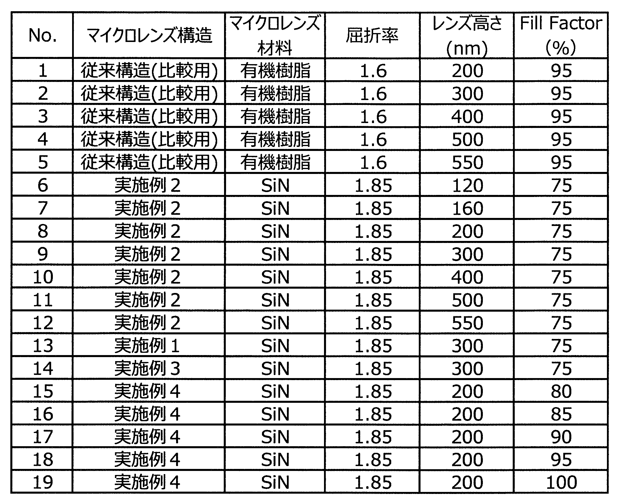
表2に、サンプルNo.1からサンプルNo.19の各固体撮像素子の受光感度評価結果を比較した結果を示す。サンプルNo.1からサンプルNo.19の各固体撮像素子の受光感度は、マイクロレンズ高さが200nmの従来構造の固体撮像素子(サンプルNo.1)の受光感度を基準とした場合の受光感度の増減量を示す。

サンプルNo.1からサンプルNo.5の結果より、従来構造ではマイクロレンズ高さを高くするほど、多くの色で受光感度が向上する結果が得られた。しかしながら、高さが550nmを超えるマイクロレンズは、プロセス上形成が困難で作製できなかった。また、サンプルNo.5の固体撮像素子(マイクロレンズ高さ550nm)は、レンズ形状が半球形状とはならずに、レンズ形状が崩れた結果となり、受光感度が低下した。今回形成した固体撮像素子よりもマイクロレンズの微細化が進んだ場合、レンズ高さが高い形状は更に形成困難となる。
次に、サンプルNo.6からサンプルNo.12の結果より、実施例2に係る構成の固体撮像素子では、マイクロレンズ高さが120nmの際にGreenの受光感度が高くなり、マイクロレンズ高さが150nm~500nmの際に従来構造(サンプルNo.1)よりも受光感度が高くなる結果が得られた。また、マイクロレンズ高さが550nmの際には、従来構造(サンプルNo.1)よりも受光感度が低下した結果であった。発明者らが知見したように、マイクロレンズの屈折率を高くした場合は、隣接画素に入射するべき光がレンズによって遮られる場合があり、全ての色フィルターで受光感度が良化しない場合があることが示された。
次に、マイクロレンズ高さが同一のサンプルNo.9、サンプルNo.13、サンプルNo.14を比較した結果、実施例1、実施例3に係る構成のサンプルNo.13、No.14で特に高い受光感度が得られることが分かった。
実施例2に係る構成のサンプルNo.9では、色フィルター100とマイクロレンズ200との間に屈折率の異なる色フィルター平坦化層40があることで、サンプルNo.13、No.14(実施例1、3)と比較して光の反射が発生して受光感度が一部低下していると思われる。また、サンプルNo.9では、色フィルター平坦化層40の膜厚を100nmで形成したことで、他の実施例の構成を有するサンプルNo.13、No.14と比較して、マイクロレンズ200から光電変換素子11までの距離が長くなっている影響も想定される。サンプルNo.9の受光感度は、サンプルNo.13の受光感度より低下するが、製造工程においては形成条件の幅が広いため、製造が容易な利点がある。
サンプルNo.14(実施例3)は、マイクロレンズを3層構造で形成したことで、高屈折率のマイクロレンズの表面で光の反射を低減する効果が得られ、サンプルNo.13(実施例1)よりも受光感度が向上している。サンプルNo.14では、プロセスの工程数が増えるものの、受光感度を向上させる構造として用いることが出来る。
サンプルNo.15~サンプルNo.19は、マイクロレンズ層を実施例4の方法で形成したことで、マイクロレンズ層のFill Factorが80%以上100%以下と高く、実施例1~3の方法で形成した場合と比較してより高い受光感度を得ることができた。
実施例2に係る構成のサンプルNo.9では、色フィルター100とマイクロレンズ200との間に屈折率の異なる色フィルター平坦化層40があることで、サンプルNo.13、No.14(実施例1、3)と比較して光の反射が発生して受光感度が一部低下していると思われる。また、サンプルNo.9では、色フィルター平坦化層40の膜厚を100nmで形成したことで、他の実施例の構成を有するサンプルNo.13、No.14と比較して、マイクロレンズ200から光電変換素子11までの距離が長くなっている影響も想定される。サンプルNo.9の受光感度は、サンプルNo.13の受光感度より低下するが、製造工程においては形成条件の幅が広いため、製造が容易な利点がある。
サンプルNo.14(実施例3)は、マイクロレンズを3層構造で形成したことで、高屈折率のマイクロレンズの表面で光の反射を低減する効果が得られ、サンプルNo.13(実施例1)よりも受光感度が向上している。サンプルNo.14では、プロセスの工程数が増えるものの、受光感度を向上させる構造として用いることが出来る。
サンプルNo.15~サンプルNo.19は、マイクロレンズ層を実施例4の方法で形成したことで、マイクロレンズ層のFill Factorが80%以上100%以下と高く、実施例1~3の方法で形成した場合と比較してより高い受光感度を得ることができた。
表2に示すように、Fill Factorが80%以上100%以下のマイクロレンズ層を有するサンプルNo.15~サンプルNo.19の固体撮像素子では、いずれの色の受光感度比較においても5%以上の増加が確認された。また、Fill Factorが80%以上100%以下のマイクロレンズ層を有する固体撮像素子では、グリーン(G)の受光感度比較は7.5%以上の増加となった。さらに、Fill Factorが85%以上95%以下のマイクロレンズ層を有するサンプルNo.16~サンプルNo.18の固体撮像素子では、いずれの色の受光感度比較も特に高い吸収率となった。
したがって、隣接する複数のレンズがそれぞれ接触しており、Fill Factorが80%以上100%以下のマイクロレンズ200を有する固体撮像素子を用いることが好ましい。また、隣接する複数のレンズがそれぞれ接触しており、色フィルターそれぞれの角部上にギャップを有し、Fill Factorが85%以上95%以下のマイクロレンズ200を有する固体撮像素子を用いることがさらに好ましい。
したがって、隣接する複数のレンズがそれぞれ接触しており、Fill Factorが80%以上100%以下のマイクロレンズ200を有する固体撮像素子を用いることが好ましい。また、隣接する複数のレンズがそれぞれ接触しており、色フィルターそれぞれの角部上にギャップを有し、Fill Factorが85%以上95%以下のマイクロレンズ200を有する固体撮像素子を用いることがさらに好ましい。
以上、各実施形態により本発明を説明したが、本発明の範囲は、図示され記載された例示的な実施形態に限定されるものではなく、本発明が目的とするものと均等な効果をもたらす全ての実施形態をも含む。さらに、本発明の範囲は、請求項により記される発明の特徴の組み合わせに限定されるものではなく、全ての開示されたそれぞれの特徴のうち特定の特徴のあらゆる所望する組み合わせによって形成されうる。
また、第1から第3の実施形態では、色フィルター100は感光性を持たせた色フィルター材料を全面に塗布し、選択的に色フィルターを形成する箇所を露光することで硬化させて、色フィルターパターンを形成した。しかしながら、色フィルター材料は、このような構成に限られない。例えば、図19に示すように、色フィルター材料に感光性を持たせずに、熱硬化性樹脂などを用いて加熱ベークで硬化した後で、フォトレジストでマスクパターンを形成して、開口したい位置の色フィルターだけをエッチングで除去するプロセスを用いても良い。またこのドライエッチングプロセスと感光性色フィルターを用いたリソグラフィプロセスを併用しても良い。また各実施形態で色フィルターの形成工程としてどれを用いても良い。また、隔壁50は色フィルター100と同様の高さとなるように形成する場合で説明するが、色フィルターの半分程度の高さの隔壁構造を用いても良い。
10・・・半導体基板
11・・・光電変換素子
12・・・素子分離構造
14・・・第1の色フィルター
15・・・第2の色フィルター
16・・・第3の色フィルター
20・・・第1のマイクロレンズ層
21・・・第2のマイクロレンズ層
22・・・第3のマイクロレンズ層
30,31,50・・・隔壁
40・・・色フィルター平坦化層
100・・・色フィルター
200・・・マイクロレンズ
300・・・マイクロレンズ平坦化層
11・・・光電変換素子
12・・・素子分離構造
14・・・第1の色フィルター
15・・・第2の色フィルター
16・・・第3の色フィルター
20・・・第1のマイクロレンズ層
21・・・第2のマイクロレンズ層
22・・・第3のマイクロレンズ層
30,31,50・・・隔壁
40・・・色フィルター平坦化層
100・・・色フィルター
200・・・マイクロレンズ
300・・・マイクロレンズ平坦化層
Claims (13)
- 半導体基板と、
前記半導体基板に設けられ、平面視でマトリクス状に配置された複数の光電変換素子と、
前記複数の光電変換素子のそれぞれに対応させて配置された複数色の色フィルターが、予め設定した規則パターンで二次元的に配置された色フィルター層と、
前記複数色の色フィルター及び前記複数の光電変換素子にそれぞれ対応させて配置された複数のレンズを有するマイクロレンズ層と、
を備え、
前記マイクロレンズ層は、前記光電変換素子側に最も近接して配置された第1のマイクロレンズ層と、前記第1のマイクロレンズ層のレンズ面上に積層するように形成された第2のマイクロレンズ層とを有し、
前記第1のマイクロレンズ層は、膜厚が150nm以上400nm以下であり、屈折率が1.75以上2.15以下であり、かつ窒化シリコンまたは窒化酸化シリコンで形成されており、
前記第2のマイクロレンズ層は、前記第1のマイクロレンズ層よりも低い屈折率を有する窒化酸化シリコンまたは酸化シリコンで形成されている固体撮像素子。 - 前記第1のマイクロレンズ層の膜厚は、150nm以上300nm以下である請求項1に記載の固体撮像素子。
- 前記第2のマイクロレンズ層の屈折率は、1.4以上1.75以下である請求項1または2に記載の固体撮像素子。
- 前記マイクロレンズ層のFill Factorが80%以上100%以下である請求項1から3のいずれか1項に記載の固体撮像素子。
- 前記マイクロレンズ層は、隣接する前記複数のレンズがそれぞれ接触しており、前記色フィルターの角部上にギャップを有する請求項1から4のいずれか1項に記載の固体撮像素子。
- 前記マイクロレンズと前記色フィルター層との間に設けられ、前記マイクロレンズと対向する面が平坦になるよう形成された色フィルター平坦化層を備える請求項1から5のいずれか1項に記載の固体撮像素子。
- 前記色フィルター平坦化層は、屈折率1.6以上1.8以下の樹脂によって形成されている請求項6に記載の固体撮像素子。
- 前記マイクロレンズ層のレンズ面上に設けられ、上面が平坦になるよう形成されたレンズ平坦化層を備える請求項1から7のいずれか1項に記載の固体撮像素子
- 前記レンズ平坦化層が、屈折率1.1以上1.6以下の樹脂によって形成されている請求項8に記載の固体撮像素子。
- 前記第2のマイクロレンズ層の膜厚は、50nm以上150nm以下である請求項1から9のいずれか1項に記載の固体撮像素子。
- 前記第1のマイクロレンズ層の膜厚に対する前記第2のマイクロレンズ層の膜厚の比率は、0.125以上1.0以下である請求項10に記載の固体撮像素子。
- 複数の光電変換素子が平面視でマトリクス状に配置され、複数の前記光電変換素子の間に素子分離構造が設けられた半導体基板上の前記光電変換素子を取り囲む位置に、隔壁を形成する工程と、
前記隔壁で囲まれた前記光電変換素子に対応する位置に、複数色の色フィルターをそれぞれ形成する工程と、
前記色フィルター及び前記隔壁の上部に、膜厚が150nm以上400nm以下である、屈折率が1.75以上2.15以下の窒化シリコン膜または窒化酸化シリコン膜を形成し、前記複数の光電変換素子にそれぞれ対応する位置に複数のレンズを形成して第1のマイクロレンズ層を形成する工程と、
前記第1のマイクロレンズ層のレンズ面上に、前記第1のマイクロレンズ層よりも低い屈折率を有する窒化酸化シリコン膜または酸化シリコン膜を形成して第2のマイクロレンズ層を形成する工程と、
を備える固体撮像素子の製造方法。 - 前記第1のマイクロレンズを形成する工程は、
色フィルター層、無機材料層、樹脂層及びレジスト層がこの順に積層された積層体の前記レジスト層に対するフォトリソグラフィにより、前記レジスト層にパターンを形成する工程と、
前記パターンを熱フローによって溶融させて、レンズ形状に成形する工程と、
前記レンズ形状に成形されたパターンをマスクとして前記樹脂層に対するドライエッチングを行い、前記樹脂層をレンズ母型に成形する工程と、
前記レンズ母型をマスクとして前記無機材料層に対するドライエッチングを行い、前記無機材料層をマイクロレンズに成形する工程と、を有する請求項12に記載の固体撮像素子の製造方法。
Priority Applications (1)
| Application Number | Priority Date | Filing Date | Title |
|---|---|---|---|
| JP2020560103A JPWO2020122032A1 (ja) | 2018-12-13 | 2019-12-09 | 固体撮像素子及び固体撮像素子の製造方法 |
Applications Claiming Priority (2)
| Application Number | Priority Date | Filing Date | Title |
|---|---|---|---|
| JP2018-233295 | 2018-12-13 | ||
| JP2018233295 | 2018-12-13 |
Publications (1)
| Publication Number | Publication Date |
|---|---|
| WO2020122032A1 true WO2020122032A1 (ja) | 2020-06-18 |
Family
ID=71077277
Family Applications (1)
| Application Number | Title | Priority Date | Filing Date |
|---|---|---|---|
| PCT/JP2019/048162 Ceased WO2020122032A1 (ja) | 2018-12-13 | 2019-12-09 | 固体撮像素子及び固体撮像素子の製造方法 |
Country Status (3)
| Country | Link |
|---|---|
| JP (1) | JPWO2020122032A1 (ja) |
| TW (1) | TW202109858A (ja) |
| WO (1) | WO2020122032A1 (ja) |
Cited By (8)
| Publication number | Priority date | Publication date | Assignee | Title |
|---|---|---|---|---|
| US20210202559A1 (en) * | 2019-12-31 | 2021-07-01 | Semiconductor Components Industries, Llc | Multi-layered microlens systems and related methods |
| JP2022030762A (ja) * | 2020-08-07 | 2022-02-18 | 凸版印刷株式会社 | 固体撮像素子 |
| JP2022030763A (ja) * | 2020-08-07 | 2022-02-18 | 凸版印刷株式会社 | 固体撮像素子 |
| JP2022075462A (ja) * | 2020-11-05 | 2022-05-18 | 采▲ぎょく▼科技股▲ふん▼有限公司 | イメージセンサおよびその形成方法 |
| JPWO2022181536A1 (ja) * | 2021-02-25 | 2022-09-01 | ||
| WO2022226726A1 (zh) * | 2021-04-26 | 2022-11-03 | 京东方科技集团股份有限公司 | 光学模组及其制作方法、显示装置 |
| CN115699315A (zh) * | 2020-06-30 | 2023-02-03 | 凸版印刷株式会社 | 固体拍摄元件 |
| US12266676B2 (en) | 2022-09-22 | 2025-04-01 | Kabushiki Kaisha Toshiba | Solid-state imaging device with anti-reflection film |
Families Citing this family (2)
| Publication number | Priority date | Publication date | Assignee | Title |
|---|---|---|---|---|
| CN115881738A (zh) * | 2021-09-26 | 2023-03-31 | 群创光电股份有限公司 | 光学感测装置 |
| US12369416B2 (en) | 2021-10-01 | 2025-07-22 | Visera Technologies Company Limited | Image sensor having dish structure formed within micro-lens |
Citations (13)
| Publication number | Priority date | Publication date | Assignee | Title |
|---|---|---|---|---|
| JP2005019573A (ja) * | 2003-06-25 | 2005-01-20 | Sanyo Electric Co Ltd | 固体撮像装置および固体撮像装置の製造方法 |
| JP2007019435A (ja) * | 2005-07-11 | 2007-01-25 | Sony Corp | 固体撮像装置およびその製造方法、並びにカメラ |
| JP2008009079A (ja) * | 2006-06-28 | 2008-01-17 | Tokyo Electron Ltd | マイクロレンズの形成方法及び半導体装置 |
| JP2008159748A (ja) * | 2006-12-22 | 2008-07-10 | Toppan Printing Co Ltd | 固体撮像素子の製造方法及び固体撮像素子 |
| JP2008277800A (ja) * | 2007-05-03 | 2008-11-13 | Dongbu Hitek Co Ltd | イメージセンサの製造方法 |
| JP2009260445A (ja) * | 2008-04-11 | 2009-11-05 | Sharp Corp | 固体撮像素子およびその製造方法、電子情報機器 |
| JP2012084608A (ja) * | 2010-10-07 | 2012-04-26 | Sony Corp | 固体撮像装置とその製造方法、並びに電子機器 |
| JP2012138412A (ja) * | 2010-12-24 | 2012-07-19 | Sharp Corp | 半導体装置及びその製造方法、固体撮像装置及びその製造方法、並びに電子情報機器 |
| JP2013077740A (ja) * | 2011-09-30 | 2013-04-25 | Sony Corp | 固体撮像素子、固体撮像素子の製造方法、及び、電子機器 |
| JP2013093371A (ja) * | 2011-10-24 | 2013-05-16 | Sony Corp | 半導体装置、および、その製造方法、固体撮像装置 |
| WO2013179972A1 (ja) * | 2012-05-30 | 2013-12-05 | ソニー株式会社 | 撮像素子、撮像装置、製造装置および方法 |
| JP2014022649A (ja) * | 2012-07-20 | 2014-02-03 | Nikon Corp | 固体撮像素子、撮像装置、及び電子機器 |
| JP2016225392A (ja) * | 2015-05-28 | 2016-12-28 | 凸版印刷株式会社 | 固体撮像素子用マイクロレンズおよび固体撮像素子用マイクロレンズの形成方法 |
Family Cites Families (4)
| Publication number | Priority date | Publication date | Assignee | Title |
|---|---|---|---|---|
| JP2010134352A (ja) * | 2008-12-08 | 2010-06-17 | Fujifilm Corp | カラーフィルタの製造方法及び固体撮像素子 |
| JP5791664B2 (ja) * | 2013-06-28 | 2015-10-07 | キヤノン株式会社 | 光学素子アレイ、及び固体撮像装置 |
| JP2015159231A (ja) * | 2014-02-25 | 2015-09-03 | パナソニックIpマネジメント株式会社 | 固体撮像装置 |
| JP6728820B2 (ja) * | 2016-03-18 | 2020-07-22 | 凸版印刷株式会社 | 固体撮像装置及びその製造方法 |
-
2019
- 2019-12-09 WO PCT/JP2019/048162 patent/WO2020122032A1/ja not_active Ceased
- 2019-12-09 JP JP2020560103A patent/JPWO2020122032A1/ja active Pending
- 2019-12-12 TW TW108145457A patent/TW202109858A/zh unknown
Patent Citations (13)
| Publication number | Priority date | Publication date | Assignee | Title |
|---|---|---|---|---|
| JP2005019573A (ja) * | 2003-06-25 | 2005-01-20 | Sanyo Electric Co Ltd | 固体撮像装置および固体撮像装置の製造方法 |
| JP2007019435A (ja) * | 2005-07-11 | 2007-01-25 | Sony Corp | 固体撮像装置およびその製造方法、並びにカメラ |
| JP2008009079A (ja) * | 2006-06-28 | 2008-01-17 | Tokyo Electron Ltd | マイクロレンズの形成方法及び半導体装置 |
| JP2008159748A (ja) * | 2006-12-22 | 2008-07-10 | Toppan Printing Co Ltd | 固体撮像素子の製造方法及び固体撮像素子 |
| JP2008277800A (ja) * | 2007-05-03 | 2008-11-13 | Dongbu Hitek Co Ltd | イメージセンサの製造方法 |
| JP2009260445A (ja) * | 2008-04-11 | 2009-11-05 | Sharp Corp | 固体撮像素子およびその製造方法、電子情報機器 |
| JP2012084608A (ja) * | 2010-10-07 | 2012-04-26 | Sony Corp | 固体撮像装置とその製造方法、並びに電子機器 |
| JP2012138412A (ja) * | 2010-12-24 | 2012-07-19 | Sharp Corp | 半導体装置及びその製造方法、固体撮像装置及びその製造方法、並びに電子情報機器 |
| JP2013077740A (ja) * | 2011-09-30 | 2013-04-25 | Sony Corp | 固体撮像素子、固体撮像素子の製造方法、及び、電子機器 |
| JP2013093371A (ja) * | 2011-10-24 | 2013-05-16 | Sony Corp | 半導体装置、および、その製造方法、固体撮像装置 |
| WO2013179972A1 (ja) * | 2012-05-30 | 2013-12-05 | ソニー株式会社 | 撮像素子、撮像装置、製造装置および方法 |
| JP2014022649A (ja) * | 2012-07-20 | 2014-02-03 | Nikon Corp | 固体撮像素子、撮像装置、及び電子機器 |
| JP2016225392A (ja) * | 2015-05-28 | 2016-12-28 | 凸版印刷株式会社 | 固体撮像素子用マイクロレンズおよび固体撮像素子用マイクロレンズの形成方法 |
Cited By (16)
| Publication number | Priority date | Publication date | Assignee | Title |
|---|---|---|---|---|
| US20210202559A1 (en) * | 2019-12-31 | 2021-07-01 | Semiconductor Components Industries, Llc | Multi-layered microlens systems and related methods |
| US11760046B2 (en) * | 2019-12-31 | 2023-09-19 | Semiconductor Components Industries, Llc | Multi-layered microlens systems and related methods |
| CN115699315A (zh) * | 2020-06-30 | 2023-02-03 | 凸版印刷株式会社 | 固体拍摄元件 |
| JP7673372B2 (ja) | 2020-08-07 | 2025-05-09 | Toppanホールディングス株式会社 | 固体撮像素子 |
| JP2022030762A (ja) * | 2020-08-07 | 2022-02-18 | 凸版印刷株式会社 | 固体撮像素子 |
| JP2022030763A (ja) * | 2020-08-07 | 2022-02-18 | 凸版印刷株式会社 | 固体撮像素子 |
| JP7729026B2 (ja) | 2020-08-07 | 2025-08-26 | Toppanホールディングス株式会社 | 固体撮像素子 |
| JP2022075462A (ja) * | 2020-11-05 | 2022-05-18 | 采▲ぎょく▼科技股▲ふん▼有限公司 | イメージセンサおよびその形成方法 |
| US11569291B2 (en) | 2020-11-05 | 2023-01-31 | Visera Technologies Company Limited | Image sensor and method forming the same |
| JP7554698B2 (ja) | 2020-11-05 | 2024-09-20 | 采▲ぎょく▼科技股▲ふん▼有限公司 | イメージセンサおよびその形成方法 |
| JPWO2022181536A1 (ja) * | 2021-02-25 | 2022-09-01 | ||
| JP7837941B2 (ja) | 2021-02-25 | 2026-03-31 | ソニーセミコンダクタソリューションズ株式会社 | 光検出装置及び電子機器 |
| CN115769107A (zh) * | 2021-04-26 | 2023-03-07 | 京东方科技集团股份有限公司 | 光学模组及其制作方法、显示装置 |
| US12265236B2 (en) | 2021-04-26 | 2025-04-01 | Boe Technology Group Co., Ltd. | Optical module, manufacturing method, and display device |
| WO2022226726A1 (zh) * | 2021-04-26 | 2022-11-03 | 京东方科技集团股份有限公司 | 光学模组及其制作方法、显示装置 |
| US12266676B2 (en) | 2022-09-22 | 2025-04-01 | Kabushiki Kaisha Toshiba | Solid-state imaging device with anti-reflection film |
Also Published As
| Publication number | Publication date |
|---|---|
| JPWO2020122032A1 (ja) | 2021-10-28 |
| TW202109858A (zh) | 2021-03-01 |
Similar Documents
| Publication | Publication Date | Title |
|---|---|---|
| WO2020122032A1 (ja) | 固体撮像素子及び固体撮像素子の製造方法 | |
| US8853758B2 (en) | Solid-state imaging device, method of manufacturing solid-state imaging device, and electronic apparatus | |
| US7683302B2 (en) | Solid-state imaging device having on-chip color filter layers and solid-state imaging device manufacturing method of the solid-state imaging device | |
| TWI488291B (zh) | 固態成像裝置,其製造方法,及電子設備 | |
| CN101901822B (zh) | 固态图像拾取装置及其制造方法、以及电子设备 | |
| TWI278991B (en) | Solid image-pickup device and method of manufacturing the same | |
| US7750360B2 (en) | Solid-state image pickup device | |
| US20120043634A1 (en) | Method of manufacturing microlens array, method of manufacturing solid-state image sensor, and solid-state image sensor | |
| US20060158547A1 (en) | Solid state imaging device and fabrication method thereof, and camera incorporating the solid state imaging device | |
| KR20140135722A (ko) | 촬상 소자 | |
| US8030117B2 (en) | Image sensor and method for manufacturing the same | |
| KR102468312B1 (ko) | 고체 촬상 소자 및 고체 촬상 소자의 제조 방법 | |
| JP2022032676A (ja) | 固体撮像素子及び固体撮像素子の製造方法 | |
| JP2000180621A (ja) | オンチップカラーフィルタ及びこれを用いた固体撮像素子 | |
| TWI775378B (zh) | 固態成像裝置 | |
| JP2005079344A (ja) | 固体撮像装置及びその製造方法 | |
| CN101183663B (zh) | 图像传感器及其制造方法 | |
| JP2008258203A (ja) | 固体撮像素子及び固体撮像素子の製造方法 | |
| KR100720509B1 (ko) | 이미지 센서 및 이의 제조 방법 | |
| JP7119557B2 (ja) | 固体撮像素子及び固体撮像素子の製造方法 | |
| US7579625B2 (en) | CMOS image sensor and method for manufacturing the same | |
| KR100720524B1 (ko) | 씨모스 이미지 센서 및 그 제조방법 | |
| KR100685874B1 (ko) | 씨모스 이미지 센서 및 그 제조방법 | |
| WO2018193986A1 (ja) | 固体撮像素子及びその製造方法 | |
| KR100731067B1 (ko) | 씨모스 이미지 센서 및 그 제조방법 |
Legal Events
| Date | Code | Title | Description |
|---|---|---|---|
| 121 | Ep: the epo has been informed by wipo that ep was designated in this application |
Ref document number: 19897490 Country of ref document: EP Kind code of ref document: A1 |
|
| ENP | Entry into the national phase |
Ref document number: 2020560103 Country of ref document: JP Kind code of ref document: A |
|
| NENP | Non-entry into the national phase |
Ref country code: DE |
|
| 122 | Ep: pct application non-entry in european phase |
Ref document number: 19897490 Country of ref document: EP Kind code of ref document: A1 |