WO2020130133A1 - 有機フォトダイオード及び赤外線cmosセンサー - Google Patents
有機フォトダイオード及び赤外線cmosセンサー Download PDFInfo
- Publication number
- WO2020130133A1 WO2020130133A1 PCT/JP2019/050075 JP2019050075W WO2020130133A1 WO 2020130133 A1 WO2020130133 A1 WO 2020130133A1 JP 2019050075 W JP2019050075 W JP 2019050075W WO 2020130133 A1 WO2020130133 A1 WO 2020130133A1
- Authority
- WO
- WIPO (PCT)
- Prior art keywords
- group
- substituent
- ring
- organic photodiode
- carbon atoms
- Prior art date
- Legal status (The legal status is an assumption and is not a legal conclusion. Google has not performed a legal analysis and makes no representation as to the accuracy of the status listed.)
- Ceased
Links
- 0 C*(C)c1c([C@@](*)C(C2*)=CC)c2c(*)c(*)c1* Chemical compound C*(C)c1c([C@@](*)C(C2*)=CC)c2c(*)c(*)c1* 0.000 description 6
- RKJHJMAZNPASHY-UHFFFAOYSA-N Cc(cc1C2)ccc1-c1c2cccc1 Chemical compound Cc(cc1C2)ccc1-c1c2cccc1 RKJHJMAZNPASHY-UHFFFAOYSA-N 0.000 description 1
- GRVMBGBDPRLWLA-UHFFFAOYSA-N Cc1cc(-c2ccc(CC3)c3c2)ccc1 Chemical compound Cc1cc(-c2ccc(CC3)c3c2)ccc1 GRVMBGBDPRLWLA-UHFFFAOYSA-N 0.000 description 1
Images
Classifications
-
- H—ELECTRICITY
- H10—SEMICONDUCTOR DEVICES; ELECTRIC SOLID-STATE DEVICES NOT OTHERWISE PROVIDED FOR
- H10F—INORGANIC SEMICONDUCTOR DEVICES SENSITIVE TO INFRARED RADIATION, LIGHT, ELECTROMAGNETIC RADIATION OF SHORTER WAVELENGTH OR CORPUSCULAR RADIATION
- H10F39/00—Integrated devices, or assemblies of multiple devices, comprising at least one element covered by group H10F30/00, e.g. radiation detectors comprising photodiode arrays
- H10F39/10—Integrated devices
- H10F39/12—Image sensors
- H10F39/191—Photoconductor image sensors
-
- C—CHEMISTRY; METALLURGY
- C08—ORGANIC MACROMOLECULAR COMPOUNDS; THEIR PREPARATION OR CHEMICAL WORKING-UP; COMPOSITIONS BASED THEREON
- C08G—MACROMOLECULAR COMPOUNDS OBTAINED OTHERWISE THAN BY REACTIONS ONLY INVOLVING UNSATURATED CARBON-TO-CARBON BONDS
- C08G73/00—Macromolecular compounds obtained by reactions forming a linkage containing nitrogen with or without oxygen or carbon in the main chain of the macromolecule, not provided for in groups C08G12/00 - C08G71/00
- C08G73/02—Polyamines
-
- C—CHEMISTRY; METALLURGY
- C08—ORGANIC MACROMOLECULAR COMPOUNDS; THEIR PREPARATION OR CHEMICAL WORKING-UP; COMPOSITIONS BASED THEREON
- C08G—MACROMOLECULAR COMPOUNDS OBTAINED OTHERWISE THAN BY REACTIONS ONLY INVOLVING UNSATURATED CARBON-TO-CARBON BONDS
- C08G73/00—Macromolecular compounds obtained by reactions forming a linkage containing nitrogen with or without oxygen or carbon in the main chain of the macromolecule, not provided for in groups C08G12/00 - C08G71/00
- C08G73/02—Polyamines
- C08G73/026—Wholly aromatic polyamines
-
- H—ELECTRICITY
- H10—SEMICONDUCTOR DEVICES; ELECTRIC SOLID-STATE DEVICES NOT OTHERWISE PROVIDED FOR
- H10K—ORGANIC ELECTRIC SOLID-STATE DEVICES
- H10K30/00—Organic devices sensitive to infrared radiation, light, electromagnetic radiation of shorter wavelength or corpuscular radiation
- H10K30/30—Organic devices sensitive to infrared radiation, light, electromagnetic radiation of shorter wavelength or corpuscular radiation comprising bulk heterojunctions, e.g. interpenetrating networks of donor and acceptor material domains
-
- H—ELECTRICITY
- H10—SEMICONDUCTOR DEVICES; ELECTRIC SOLID-STATE DEVICES NOT OTHERWISE PROVIDED FOR
- H10K—ORGANIC ELECTRIC SOLID-STATE DEVICES
- H10K85/00—Organic materials used in the body or electrodes of devices covered by this subclass
- H10K85/10—Organic polymers or oligomers
- H10K85/111—Organic polymers or oligomers comprising aromatic, heteroaromatic, or aryl chains, e.g. polyaniline, polyphenylene or polyphenylene vinylene
-
- H—ELECTRICITY
- H10—SEMICONDUCTOR DEVICES; ELECTRIC SOLID-STATE DEVICES NOT OTHERWISE PROVIDED FOR
- H10K—ORGANIC ELECTRIC SOLID-STATE DEVICES
- H10K85/00—Organic materials used in the body or electrodes of devices covered by this subclass
- H10K85/10—Organic polymers or oligomers
- H10K85/111—Organic polymers or oligomers comprising aromatic, heteroaromatic, or aryl chains, e.g. polyaniline, polyphenylene or polyphenylene vinylene
- H10K85/113—Heteroaromatic compounds comprising sulfur or selene, e.g. polythiophene
-
- H—ELECTRICITY
- H10—SEMICONDUCTOR DEVICES; ELECTRIC SOLID-STATE DEVICES NOT OTHERWISE PROVIDED FOR
- H10K—ORGANIC ELECTRIC SOLID-STATE DEVICES
- H10K85/00—Organic materials used in the body or electrodes of devices covered by this subclass
- H10K85/10—Organic polymers or oligomers
- H10K85/141—Organic polymers or oligomers comprising aliphatic or olefinic chains, e.g. poly N-vinylcarbazol, PVC or PTFE
-
- H—ELECTRICITY
- H10—SEMICONDUCTOR DEVICES; ELECTRIC SOLID-STATE DEVICES NOT OTHERWISE PROVIDED FOR
- H10K—ORGANIC ELECTRIC SOLID-STATE DEVICES
- H10K85/00—Organic materials used in the body or electrodes of devices covered by this subclass
- H10K85/10—Organic polymers or oligomers
- H10K85/151—Copolymers
-
- H—ELECTRICITY
- H10—SEMICONDUCTOR DEVICES; ELECTRIC SOLID-STATE DEVICES NOT OTHERWISE PROVIDED FOR
- H10K—ORGANIC ELECTRIC SOLID-STATE DEVICES
- H10K85/00—Organic materials used in the body or electrodes of devices covered by this subclass
- H10K85/40—Organosilicon compounds, e.g. TIPS pentacene
-
- H—ELECTRICITY
- H10—SEMICONDUCTOR DEVICES; ELECTRIC SOLID-STATE DEVICES NOT OTHERWISE PROVIDED FOR
- H10K—ORGANIC ELECTRIC SOLID-STATE DEVICES
- H10K85/00—Organic materials used in the body or electrodes of devices covered by this subclass
- H10K85/60—Organic compounds having low molecular weight
- H10K85/615—Polycyclic condensed aromatic hydrocarbons, e.g. anthracene
- H10K85/626—Polycyclic condensed aromatic hydrocarbons, e.g. anthracene containing more than one polycyclic condensed aromatic rings, e.g. bis-anthracene
-
- H—ELECTRICITY
- H10—SEMICONDUCTOR DEVICES; ELECTRIC SOLID-STATE DEVICES NOT OTHERWISE PROVIDED FOR
- H10K—ORGANIC ELECTRIC SOLID-STATE DEVICES
- H10K85/00—Organic materials used in the body or electrodes of devices covered by this subclass
- H10K85/60—Organic compounds having low molecular weight
- H10K85/649—Aromatic compounds comprising a hetero atom
- H10K85/655—Aromatic compounds comprising a hetero atom comprising only sulfur as heteroatom
-
- H—ELECTRICITY
- H10—SEMICONDUCTOR DEVICES; ELECTRIC SOLID-STATE DEVICES NOT OTHERWISE PROVIDED FOR
- H10K—ORGANIC ELECTRIC SOLID-STATE DEVICES
- H10K85/00—Organic materials used in the body or electrodes of devices covered by this subclass
- H10K85/60—Organic compounds having low molecular weight
- H10K85/649—Aromatic compounds comprising a hetero atom
- H10K85/657—Polycyclic condensed heteroaromatic hydrocarbons
- H10K85/6576—Polycyclic condensed heteroaromatic hydrocarbons comprising only sulfur in the heteroaromatic polycondensed ring system, e.g. benzothiophene
-
- H—ELECTRICITY
- H10—SEMICONDUCTOR DEVICES; ELECTRIC SOLID-STATE DEVICES NOT OTHERWISE PROVIDED FOR
- H10K—ORGANIC ELECTRIC SOLID-STATE DEVICES
- H10K30/00—Organic devices sensitive to infrared radiation, light, electromagnetic radiation of shorter wavelength or corpuscular radiation
- H10K30/20—Organic devices sensitive to infrared radiation, light, electromagnetic radiation of shorter wavelength or corpuscular radiation comprising organic-organic junctions, e.g. donor-acceptor junctions
-
- H—ELECTRICITY
- H10—SEMICONDUCTOR DEVICES; ELECTRIC SOLID-STATE DEVICES NOT OTHERWISE PROVIDED FOR
- H10K—ORGANIC ELECTRIC SOLID-STATE DEVICES
- H10K39/00—Integrated devices, or assemblies of multiple devices, comprising at least one organic radiation-sensitive element covered by group H10K30/00
- H10K39/30—Devices controlled by radiation
- H10K39/32—Organic image sensors
-
- Y—GENERAL TAGGING OF NEW TECHNOLOGICAL DEVELOPMENTS; GENERAL TAGGING OF CROSS-SECTIONAL TECHNOLOGIES SPANNING OVER SEVERAL SECTIONS OF THE IPC; TECHNICAL SUBJECTS COVERED BY FORMER USPC CROSS-REFERENCE ART COLLECTIONS [XRACs] AND DIGESTS
- Y02—TECHNOLOGIES OR APPLICATIONS FOR MITIGATION OR ADAPTATION AGAINST CLIMATE CHANGE
- Y02E—REDUCTION OF GREENHOUSE GAS [GHG] EMISSIONS, RELATED TO ENERGY GENERATION, TRANSMISSION OR DISTRIBUTION
- Y02E10/00—Energy generation through renewable energy sources
- Y02E10/50—Photovoltaic [PV] energy
- Y02E10/549—Organic PV cells
Definitions
- the present invention relates to an organic photodiode (organic photoelectric conversion element) and an infrared CMOS sensor using this organic photodiode. Specifically, the present invention relates to an organic photodiode that achieves both high photoelectric conversion efficiency and low dark current value, and an infrared CMOS sensor that uses this organic photodiode.
- CMOS image sensors are used as image sensors in digital cameras and smartphones.
- the CMOS sensor has a high sensitivity that can be photographed even in a low illuminance, a high dynamic range that can simultaneously capture a mixture of bright and dark images, a simultaneous exposure batch readout (global shutter) function, and a high frame that can track a fast-moving subject. Rates are required.
- the organic photoelectric conversion film is considered to be suitable for CMOS sensor applications from the following points. -Compared to Si photodiodes, they can be made thinner, allowing a wider incident angle and reliably photoelectrically converting a small amount of light. Since the signal storage thick photoelectric conversion unit can be designed independently, the capacity of the signal storage unit can be increased and a high dynamic range can be easily achieved. -The signal storage unit can be used as it is as a memory.
- CMOS sensors using organic photoelectric conversion films have expanded in recent years. There, by using an image different from the image by visible light, especially by using near-infrared rays, it is possible to detect a person on a night road that is difficult to see with the naked eye, or to confirm the crop harvest level from the image of the field, or simply with the naked eye. It is expected to be applied to security applications such as seeing the opposite side through a wall that can only be seen in black. This is because it is said that it is preferable to use the organic photoelectric conversion film because the sensor using silicon has low infrared sensitivity.
- a CMOS sensor using an organic photoelectric conversion film can be thinned, but on the other hand, problems such as short-circuiting of elements and leakage current (dark current) that occur due to thinning occur.
- the smoothing of the electrode exerts a great effect. For example, by providing a coating film on the electrodes, a short circuit preventing effect is obtained.
- the photoelectric conversion layer When the photoelectric conversion layer is divided into a layer having substantially only a p-type semiconductor and a layer having substantially only an n-type semiconductor, the dark current can be suppressed to a low value. It becomes less efficient.
- the photoelectric conversion efficiency is excellent, but there is a problem of dark current generation.
- Non-Patent Document 1 reports on the relationship between the dark current and the Ip difference between the hole blocking layer and the photoelectric conversion layer (quinacridone).
- the dark current density is reduced to about 1 ⁇ 10 ⁇ 7 A/cm 2 due to the presence of the blocking layer.
- Patent Document 1 a structure in which a current blocking layer (a hole blocking layer and an electron blocking layer) is provided on both surfaces of a photoelectric conversion layer is also proposed.
- the dark current density in Patent Document 1 is about 1 ⁇ 10 ⁇ 7 A/cm 2 even at a low level, and it has not reached the level currently required.
- the electron blocking layer 5 has a lower energy level HOMO and a higher energy level LUMO than the p-type semiconductor layer 7 of the photoelectric conversion layer 3'.
- the photoelectric conversion layer 3' is equivalent to the electron blocking layer 5".
- the hole blocking layer 6 is provided to reduce dark current due to holes injected from the upper electrode 4, and prevents holes from the upper electrode 4 from being injected into the photoelectric conversion layer 3. To do.
- hole blocking layer is effective in reducing the dark current, but specific examples of the hole blocking layer are described in the paragraph [0042], "hole blocking layer.” 6 is preferably an organic substance such as copper phthalocyanine, PTCDA, an acetylacetonate complex, BCP or Alq, an organic-metal compound, or an inorganic substance such as MgAg or MgO.”
- Patent Document 3 also discloses a structure in which blocking layers are provided on both surfaces of a photoelectric conversion layer.
- the dark current value is small but the efficiency is low, and 10% in the infrared region. It's just a degree.
- the efficiency is good, but the dark current value is ⁇ 1 V, 1 ⁇ 10 ⁇ 5 A/cm 2 to 1 ⁇ 10 ⁇ 6. Very high at about A/cm 2 .
- An object of the present invention is to provide an organic photodiode capable of reducing a dark current value while maintaining high photoelectric conversion efficiency, and an infrared CMOS sensor using this organic photodiode.
- the present inventor compares photoelectric conversion efficiencies by providing a photoelectric conversion layer with a bulk heterojunction structure containing a p-type semiconductor and an n-type semiconductor and then providing a hole transport layer containing a specific polymer compound as a blocking layer. It has succeeded in suppressing the dark current density to 10 ⁇ 7 A/cm 2 or less while maintaining a relatively high state. That is, the gist of the present invention is as follows.
- An organic photodiode including a first electrode, a hole transport layer, a photoelectric conversion layer, and a second electrode in this order, wherein the photoelectric conversion layer includes a p-type semiconductor and an n-type semiconductor,
- the pore transport layer contains a polymer compound containing a repeating unit represented by the following formula (2), and the polymer compound has a group in which carbon atoms of side chains are mutually bonded at 230° C. between the polymer compounds.
- An organic photodiode comprising:
- m represents an integer of 0 to 3.
- Ar 11 and Ar 12 each independently represent a direct bond, an aromatic hydrocarbon group which may have a substituent or an aromatic heterocyclic group which may have a substituent.
- Ar 13 to Ar 15 each independently represent an aromatic hydrocarbon group which may have a substituent or an aromatic heterocyclic group which may have a substituent.
- the m Ar 14s and the Ar 15s may be the same or different. However, Ar 11 and Ar 12 are not a direct bond at the same time.
- Ar 1 represents an aromatic hydrocarbon group which may have a substituent or an aromatic heterocyclic group which may have a substituent.
- n represents an integer of 1 to 6.
- the n Ar 1 s may be the same or different, and the benzocyclobutene ring in formula (1A) may have a substituent.
- the substituents may combine with each other to form a ring.
- R 3 to R 5 represent a hydrogen atom or an alkyl group.
- R 6 , R 7 and R 10 represent a hydrogen atom, an alkyl group or an alkoxy group.
- r and j are integers of 1 to 5, and k is an integer of 1 to 7.
- R 6 s When r is 2 or more, plural R 6 s may be the same or different, and adjacent R 6 s may be bonded to each other to form a ring.
- R 7 s When j is 2 or more, plural R 7 s may be the same or different, and adjacent R 7 s may be bonded to each other to form a ring.
- k is 2 or more, a plurality of R 10's may be the same or different.
- Ar 2 represents an aromatic hydrocarbon group which may have a substituent or an aromatic heterocyclic group which may have a substituent.
- D represents a donor moiety having a polycyclic aromatic group.
- A represents an acceptor moiety having a malononitrile group.
- Ar 41 is independently represented by the following formulas (5a-1) to (5g-1).
- Ar 42 is independently represented by the following formulas (5a-2) to (5d-2).
- Ar 43 is independently represented by the following formulas (5a-3) to (5d-3).
- Y represents CR 31 R 31 , SiR 31 R 31 , GeR 31 R 31 , NR 31 , or C ⁇ O.
- Z represents CR 31 or N.
- L represents R 31 or a halogen atom.
- Each R 31 independently has a hydrogen atom, an optionally branched alkyl group having 1 to 30 carbon atoms, an optionally branched alkoxy group having 1 to 30 carbon atoms, or a branched one.
- A represents an acceptor moiety having a malononitrile group.
- x1 represents 0 or 1
- x2 represents an integer of 1 to 6
- x3 represents 0 or 1.
- Expression (5f-1) and Expression (5g-1) are not adjacent to each other.
- * represents a binding site.
- Each R A independently represents a hydrogen atom, a halogen atom, an optionally branched alkyl group having 1 to 30 carbon atoms, an optionally branched alkoxy group having 1 to 30 carbon atoms, or a branched chain. It represents a phenyl group which may be substituted with an optionally substituted alkyl group having 1 to 30 carbon atoms and/or an optionally branched alkoxy group having 1 to 30 carbon atoms.
- R B has the same meaning as R A , or adjacent R B forms an aromatic 6-membered ring.
- the polymer compound has a weight average molecular weight (Mw) of 20,000 or more and a dispersity (Mw/Mn) of 2.5 or less (where Mn represents a number average molecular weight) [1] to The organic photodiode according to any one of [7].
- p represents an integer of 1 or more and 6 or less
- q represents an integer of 0 or more and 3 or less.
- Ar 21 and Ar 22 each independently represent a direct bond, an aromatic hydrocarbon group which may have a substituent or an aromatic heterocyclic group which may have a substituent.
- Ar 23 to Ar 27 each independently represent an aromatic hydrocarbon group which may have a substituent or an aromatic heterocyclic group which may have a substituent.
- R 1 is a hydrogen atom, an alkyl group having 1 to 24 carbon atoms which may have a substituent, an alkoxy group having 1 to 24 carbon atoms which may have a substituent, or a substituent. It represents a good aromatic hydrocarbon group or an aromatic heterocyclic group which may have a substituent.
- the p Ar 27 s may be the same or different.
- the q Ar 24's and Ar 25's may be the same or different.
- Ar 21 and Ar 22 are not direct bonds at the same time.
- the proportion of the n-type semiconductor having a fullerene skeleton is 10% by weight or less with respect to the n-type semiconductor having no fullerene skeleton, [1] to [10] Organic photodiode.
- an organic photodiode having a high photoelectric conversion efficiency and a low dark current value.
- a high performance infrared CMOS sensor can be provided using the organic photodiode of the present invention.
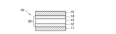
- FIG. 1 is a schematic cross-sectional view showing an example of the embodiment of the organic photodiode of the present invention.
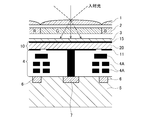
- FIG. 2 is a schematic cross-sectional view showing an example of the structure of the infrared CMOS sensor of the present invention using the organic photodiode of the present invention.
- the organic photodiode of the present invention is an organic photodiode including a first electrode, a hole transport layer, a photoelectric conversion layer, and a second electrode in this order, wherein the photoelectric conversion layer is a p-type semiconductor and an n-type semiconductor.
- the hole transport layer contains a polymer compound containing a repeating unit represented by the following formula (2), and the polymer compounds have side chains at 230° C. between the polymer compounds. It has a group bonded to the carbon atom of.
- a polymer compound containing a repeating unit represented by the following formula (2) which also includes a hole transport layer according to the present invention, wherein carbon atoms of side chains between the polymer compounds are 230°C.
- the polymer compound having a group that binds to may be referred to as the “hole transporting polymer of the present invention”.
- m represents an integer of 0 to 3.
- Ar 11 and Ar 12 each independently represent a direct bond, an aromatic hydrocarbon group which may have a substituent or an aromatic heterocyclic group which may have a substituent.
- Ar 13 to Ar 15 each independently represent an aromatic hydrocarbon group which may have a substituent or an aromatic heterocyclic group which may have a substituent.
- the m Ar 14s and the Ar 15s may be the same or different. However, Ar 11 and Ar 12 are not a direct bond at the same time.
- FIG. 1 is a schematic sectional view showing an example of the organic photodiode of the present invention.
- a first electrode 11, a hole transport layer 12, a photoelectric conversion layer 13, an electron transport layer 14, and a second electrode 15 as a lower electrode are laminated in this order.
- the hole transport layer 12, the photoelectric conversion layer 13, and the electron transport layer 14 form the organic photoelectric film 20.
- a substrate is provided on the side of the first electrode 11 opposite to the hole transport layer 12. It is preferable to provide the hole transport layer according to the present invention on the first electrode formed on the substrate because the smoothness of the substrate affects the hole transport layer side to form a uniform layer.
- the hole-transporting polymer of the present invention having a group to be bonded hereinafter, these groups may be simply referred to as "groups bonded to carbon atoms of side chains at 230°C" will be described.
- Ar 1 represents an aromatic hydrocarbon group which may have a substituent or an aromatic heterocyclic group which may have a substituent.
- n represents an integer of 1 to 6.
- the n Ar 1 s may be the same or different, and the benzocyclobutene ring in formula (1A) may have a substituent.
- the substituents may combine with each other to form a ring.
- R 3 to R 5 represent a hydrogen atom or an alkyl group.
- R 6 , R 7 and R 10 represent a hydrogen atom, an alkyl group or an alkoxy group.
- r and j are integers of 1 to 5, and k is an integer of 1 to 7.
- R 6 s When r is 2 or more, plural R 6 s may be the same or different, and adjacent R 6 s may be bonded to each other to form a ring.
- R 7 s When j is 2 or more, plural R 7 s may be the same or different, and adjacent R 7 s may be bonded to each other to form a ring.
- k is 2 or more, a plurality of R 10's may be the same or different.
- Ar 2 represents an aromatic hydrocarbon group which may have a substituent or an aromatic heterocyclic group which may have a substituent.
- bonding to side-chain carbon atoms at 230° C. to each other means that the hole-transporting polymer of the present invention is polymerized to be insolubilized at 230° C., which is a temperature at which ring-opening and polymerization are performed.
- the subsequent process leads to the possibility of stacking by coating, which is effective in adopting the coating process.
- the groups can bond to carbon atoms of side chains with each other at a lower temperature of 200°C.
- one having ordinary skill in the art can easily discriminate whether or not there are groups that bond to carbon atoms of side chains at 230° C., but if it is difficult to discriminate from the entire structure, You can check it in this way.
- an appropriate amount of the polymer compound is dissolved in toluene, and the solution is applied to a substrate and then dried by heating at 230° C. for 1 hour to obtain a film having a film thickness of 25 nm to 100 nm. It can be confirmed that it does not substantially dissolve even when kept inside. In this case, it can be confirmed by cross-section SEM observation that the film is not substantially dissolved in toluene and the film thickness is hardly reduced.
- the group which the hole transporting polymer of the present invention has, at 230° C., bonded to the carbon atoms of the side chains, is a group in which the polymer compounds are polymerized by ring-opening. It is preferable from the viewpoint of multilayer coating in the process. Therefore, a group represented by any of the above formulas (1A) to (1I) is preferable, and more preferably a group represented by the above formula (1A), (1G), (1H), (1I) having a cyclobutene group. It is a base.
- the hole-transporting polymer (1A) of the present invention has a benzocyclobutene ring with a carbon atom in the main chain via Ar 1 which is 1 to 6 aromatic hydrocarbon groups or aromatic heterocyclic groups. Exists.
- the hole transporting polymer (1A) of the present invention has 1 to 6 aromatic hydrocarbon groups or aromatic heterocyclic groups interposed between the main chain and the crosslinkable group, the main chains have a suitable amount. Since they are separated from each other, aggregation does not occur, and hole transfer between crosslinked main chains is also promoted. Further, since the main chain and the crosslinkable group have a rigid structure, they are also excellent in heat resistance.
- the hole-transporting polymer (1A) of the present invention has 1 to 6 aromatic hydrocarbon groups or aromatic heterocyclic groups via the carbon atom which is the center of the sp 3 hybrid orbital present in the main chain, The presence of a benzocyclobutene ring is preferred.
- the crosslinkable group that is the side chain that bonds to the carbon atom that is the center of the sp 3 hybrid orbital does not hinder the hole transport. Therefore, the hole-transporting polymer and the network polymer obtained by crosslinking the hole-transporting polymer are further improved in the hole-transporting property.
- the atom at the center of the sp 3 hybrid orbital existing in the main chain of the polymer is more likely to rotate the bond around it than the atom at the center of the sp 2 hybrid orbital. Therefore, since the crosslinkable group in the hole transporting polymer reacts efficiently, it is hardly soluble in an organic solvent even if the number of crosslinkable groups is small or the conditions of the crosslink reaction are mild. be able to.
- Examples of the substituent which the benzocyclobutene ring in the formula (1A) may have in addition to Ar 1 include those described in the section of [Substituent group Z] described later. It is preferable that the benzocyclobutene ring in the formula (1A) does not have a substituent other than Ar 1 from the viewpoint that the steric hindrance due to the substituent and the influence of the electronic effect of the substituent upon the crosslinking reaction are small.
- Ar 1 represents an aromatic hydrocarbon group which may have a substituent or an aromatic heterocyclic group which may have a substituent.
- Examples of the aromatic hydrocarbon group for Ar 1 include a benzene ring, a naphthalene ring, an anthracene ring, a phenanthrene ring, a perylene ring, a tetracene ring, a pyrene ring, a benzpyrene ring, a chrysene ring, a triphenylene ring, an acenaphthene ring, a fluoranthene ring and a fluorene ring.
- Examples thereof include a monovalent 6-membered ring or a monovalent group having 2 to 5 condensed rings, such as a ring.
- Examples of the aromatic heterocyclic group for Ar 1 include a furan ring, a benzofuran ring, a thiophene ring, a benzothiophene ring, a pyrrole ring, a pyrazole ring, an imidazole ring, an oxadiazole ring, an indole ring, a carbazole ring, and a pyrroloimidazole ring.
- Examples of the condensed ring include monovalent or higher valent groups.
- Ar 1 is preferably a ring-derived group selected from the group consisting of a benzene ring, a naphthalene ring, an anthracene ring, and a phenanthrene ring, and a group derived from a benzene ring. That is, it is most preferably a phenylene group.
- the substituent that the aromatic hydrocarbon group or aromatic heterocyclic group of Ar 1 may have is not particularly limited, and examples thereof include groups selected from the following substituent group Z.
- the substituent is preferably an alkyl group, an alkoxy group, an aromatic hydrocarbon group or an aromatic heterocyclic group.
- the carbon number of Ar 1 including the substituent is usually 3 or more, preferably 5 or more, more preferably 6 or more, and usually 36 or less, from the viewpoint of excellent hole transportability and durability. Is 24 or less, more preferably 12 or less.
- [Substituent group Z] For example, methyl group, ethyl group, n-propyl group, i-propyl group, n-butyl group, i-butyl group, sec-butyl group, tert-butyl group, n-hexyl group, cyclohexyl group, dodecyl group, A linear, branched or cyclic alkyl group having a carbon number of usually 1 or more and usually 24 or less, preferably 12 or less; An alkenyl group having a carbon number of usually 2 or more and usually 24 or less, preferably 12 or less, such as a vinyl group; An alkynyl group having a carbon number of usually 2 or more and usually 24 or less, preferably 12 or less, such as an ethynyl group; An alkoxy group having a carbon number of usually 1 or more and usually 24 or less, preferably 12 or less, such as a methoxy group and an ethoxy group; An ary
- each of the above substituents may further have a substituent, and examples thereof are selected from the groups exemplified in the item of the substituent group Z.
- n represents an integer of 1 or more and 6 or less.
- N is preferably an integer of 1 or more and 3 or less from the viewpoint that the crosslinking reaction is likely to proceed and that the main chain is not aggregated or separated too much after the crosslinking reaction and the hole transport property is excellent.
- n Ar 1 s may be the same or different.
- the hole transporting polymer of the present invention may have a group represented by any of the above formulas (1B) to (1I) in place of the group represented by the formula (1A), It may have a group represented by the formula (1A) and a group represented by any of the formulas (1B) to (1I).
- the alkyl group represented by R 3 to R 7 and R 10 in the formulas (1B), (1C), (1F) to (1I) is usually a linear or branched chain alkyl group having 6 or less carbon atoms.
- a group is preferable, and examples thereof include a methyl group, an ethyl group, an n-propyl group, a 2-propyl group, an n-butyl group and an isobutyl group. More preferably, it is a methyl group or an ethyl group.
- a linear or branched chain alkoxy group having 6 or less carbon atoms is usually preferable, and examples thereof include a methoxy group, an ethoxy group, an n-propoxy group, and 2-propoxy group. Group, n-butoxy group and the like. More preferably, it is a methoxy group or an ethoxy group.
- the carbon number of R 6 , R 7 and R 10 is 6 or less, the cross-linking reaction is not sterically hindered and the formed film tends to be insolubilized.
- aromatic hydrocarbon group which may have a substituent of Ar 2 in the formula (1E) for example, a 6-membered monocyclic ring having one free valence, such as a benzene ring and a naphthalene ring. Alternatively, 2 to 5 condensed rings may be mentioned. Particularly preferred is a benzene ring having one free valence.
- Ar 2 may be a group in which two or more aromatic hydrocarbon groups which may have a substituent are bonded. Examples of such a group include a biphenylene group and a terphenylene group, and a 4,4′-biphenylene group is preferable.
- a cyclic ether group such as an epoxy group and an oxetane group
- a group that undergoes a crosslinking reaction by cationic polymerization such as a vinyl ether group
- a vinyl ether group has high reactivity and are insolubilized by the crosslinking. Is preferable because it is easy.
- an oxetane group is more preferable in that the rate of cationic polymerization can be easily controlled
- a vinyl ether group is preferable in that it is difficult to generate a hydroxyl group that may lead to deterioration of the device during cationic polymerization.
- An aryl vinyl carbonyl group such as a cinnamoyl group, a benzocyclobutene ring having a monovalent free valence, and a group capable of cycloaddition reaction such as a 1,2-dihydrocyclobuta[a]naphthalene ring having a monovalent free valence; It is preferable in that it further improves the electrochemical stability of the device.
- a cyclobutene ring condensed to an aromatic ring having a monovalent free valence and a 1,2-dihydro having a monovalent free valence in that the structure after crosslinking is particularly stable.
- a group containing a cyclobuta[a]naphthalene ring is preferred.
- a benzocyclobutene ring or a 1,2-dihydrocyclobuta[a]naphthalene ring having a monovalent free valence is more preferable, and a 1,2-dihydro having a monovalent free valence at a low crosslinking reaction temperature.
- the cyclobuta[a]naphthalene ring is particularly preferred.
- the hole transporting polymer of the present invention contains the repeating unit represented by the above formula (2).
- the hole-transporting polymer of the present invention has an amine structure in the main chain and has a nitrogen atom that is the center of the sp 3 hybrid orbital, and thus has excellent hole-transporting properties and electrical durability.
- Ar 11 to Ar 15 are each independently a direct bond, an aromatic hydrocarbon group which may have a substituent, or an aromatic heterocycle which may have a substituent. Represents a group. Ar 11 and Ar 12 are not direct bonds at the same time. Ar 13 to Ar 15 each independently represent an aromatic hydrocarbon group which may have a substituent or an aromatic heterocyclic group which may have a substituent.
- Examples of the aromatic hydrocarbon group which may have a substituent of Ar 11 to Ar 15 include, for example, benzene ring, naphthalene ring, anthracene ring, phenanthrene ring, perylene ring, tetracene ring, pyrene ring, benzpyrene ring, chrysene.
- Examples thereof include a 6-membered monocyclic ring or a group derived from 2 to 5 condensed rings such as a ring, a triphenylene ring, an acenaphthene ring, a fluoranthene ring, and a fluorene ring.
- Examples of the aromatic heterocyclic group which may have a substituent of Ar 11 to Ar 15 include, for example, a furan ring, a benzofuran ring, a thiophene ring, a benzothiophene ring, a pyrrole ring, a pyrazole ring, an imidazole ring and an oxadiazole ring.
- Ar 11 to Ar 15 each independently comprise a benzene ring, a naphthalene ring, an anthracene ring, a phenanthrene ring, a triphenylene ring, a pyrene ring, a thiophene ring, a pyridine ring or a fluorene ring.
- a ring-derived group selected from the group is preferred.
- a group in which one kind or two or more kinds of rings selected from the above group are linked by a direct bond is also preferable, and a biphenyl group, a biphenylene group, a terphenyl group, and a terphenylene group are more preferable.
- the carbon number of Ar 11 to Ar 15 including the substituent is usually 3 or more, preferably 5 or more, more preferably 6 or more, and usually 72 or less, preferably 48 or less, from the viewpoint of excellent hole transportability. , And more preferably 25 or less.
- [3-2. m] M in Formula (2) represents an integer of 0 or more and 3 or less.
- m is 0 from the viewpoint that the solubility of the crosslinkable polymer in an organic solvent and the film forming property are enhanced. From the viewpoint of improving the hole transport ability of the polymer, m is preferably 1 or more and 3 or less.
- the repeating unit represented by the formula (2) has 2 or more Ar 14 and Ar 15 .
- Ar 14's and Ar 15's may be the same or different.
- Ar 14's and Ar 15's may be bonded to each other directly or via a linking group to form a cyclic structure.
- the hole-transporting polymer of the present invention preferably contains a repeating unit represented by the following formula (3) from the viewpoint of excellent hole-transporting property and electrical durability.
- p represents an integer of 1 or more and 6 or less
- q represents an integer of 0 or more and 3 or less.
- Ar 21 and Ar 22 each independently represent a direct bond, an aromatic hydrocarbon group which may have a substituent or an aromatic heterocyclic group which may have a substituent.
- Ar 23 to Ar 27 each independently represent an aromatic hydrocarbon group which may have a substituent or an aromatic heterocyclic group which may have a substituent.
- R 1 is a hydrogen atom, an alkyl group having 1 to 24 carbon atoms which may have a substituent, an alkoxy group having 1 to 24 carbon atoms which may have a substituent, or a substituent. It represents a good aromatic hydrocarbon group or an aromatic heterocyclic group which may have a substituent.
- the p Ar 27 s may be the same or different.
- the q Ar 24's and Ar 25's may be the same or different.
- Ar 21 and Ar 22 are not direct bonds at the same time.
- Ar 21 to Ar 26 , q each independently represent a direct bond, an aromatic hydrocarbon group which may have a substituent, or an aromatic heterocycle which may have a substituent. Represents a group. Ar 21 and Ar 22 are not direct bonds at the same time.
- Ar 23 to Ar 26 each independently represent an aromatic hydrocarbon group which may have a substituent or an aromatic heterocyclic group which may have a substituent.
- Ar 21 to Ar 26 are the same as those of Ar 11 to Ar 15 described above.
- Q in the formula (3) represents an integer of 0 or more and 3 or less. From the viewpoint of improving the solubility of the polymer in an organic solvent and the film forming property, q is preferably 0. From the viewpoint of improving the hole transport ability of the polymer, q is preferably 1 or more and 3 or less.
- the repeating unit represented by the formula (3) has two or more Ar 24 and Ar 25 .
- Ar 24's and Ar 25's may be the same or different.
- Ar 24's and Ar 25's may be bonded to each other directly or via a linking group to form a cyclic structure.
- Ar 27 , p] (Ar 27 )p in formula (3) is a group that bonds to the carbon atom that is the center of the sp 3 hybrid orbital and the benzocyclobutene ring, and is (Ar 1 ) n in formula (1A).
- Ar 27 represents an aromatic hydrocarbon group which may have a substituent or an aromatic heterocyclic group which may have a substituent.
- p represents an integer of 0 or more and 6 or less.
- the p Ar 27 s may be the same or different. Specific examples and preferable examples of Ar 27 are the same as those of Ar 1 described above.
- R 1 is a hydrogen atom, an alkyl group having 1 to 24 carbon atoms which may have a substituent, an alkoxy group having 1 to 24 carbon atoms which may have a substituent, or a substituent. It represents a good aromatic hydrocarbon group or an aromatic heterocyclic group which may have a substituent. Of these, an alkyl group is preferable because of its excellent hole transporting property and high solubility before the crosslinking reaction.
- alkyl group examples include methyl group, ethyl group, n-propyl group, i-propyl group, n-butyl group, i-butyl group, sec-butyl group, tert-butyl group, n-hexyl group, cyclohexyl group and dodecyl group.
- a group such as a group having a carbon number of usually 1 or more and usually 24 or less, preferably 12 or less is preferable.
- the alkoxy group is preferably a group having a carbon number of usually 1 or more, usually 24 or less, preferably 12 or less, such as a methoxy group and an ethoxy group.
- substituent examples include a group selected from the above-mentioned substituent group Z, and an alkyl group, an alkoxy group, an aromatic hydrocarbon group and an aromatic heterocyclic group are preferable.
- aromatic hydrocarbon group which may have a substituent and the aromatic heterocyclic group which may have a substituent are the same as those described above for Ar 11 to Ar 15. The same is true.
- the hole-transporting polymer of the present invention contains a monovalent or divalent or higher valent group derived from a fluorene ring as a partial structure, in addition to the excellent hole-transporting property and the excellent solubility before the crosslinking reaction. preferable.
- the number of groups bonded to carbon atoms of side chains at 230° C. such as groups represented by any one of formulas (1A) to (1I), per 1000 molecular weight of the hole transporting polymer (hereinafter, referred to as “ The formula (1) number/1000” may be referred to as “the number of monomers/1000”.) can be calculated from the molar ratio of the charged monomers at the time of synthesis, excluding the terminal group from the hole-transporting polymer, and the structural formula.
- the case of the polymer (H1) represented by the formula (H1) used in Example 2 described later will be described.
- the molecular weight excluding the terminal groups is 503.42, and the number of groups represented by the formula (1A) is 0.05 on average per molecule.
- the number of groups represented by the formula (1A) per molecular weight 1000 is calculated to be 0.1.
- the number of the groups represented by any one of the formulas (1A) to (1I) in the hole-transporting polymer of the present invention is usually 3.0 or less, preferably 2.0 or less, per 1000 molecular weight. It is preferably 1.0 or less, usually 0.01 or more, and preferably 0.05 or more.
- the number of formulas (1)/1000 exceeds the above upper limit value, a flat film cannot be obtained due to cracks, or the crosslink density becomes too high, and unreacted formulas (1A) to (1I) are present in the crosslink layer. 2) increases the number of groups represented by any of the above), and may affect the life of the obtained organic photodiode.
- the number of formulas (1)/1000 is less than the above lower limit value, the insolubilization of the crosslinked layer becomes insufficient, and there is a possibility that a multilayer laminated structure cannot be formed by a wet film forming method.
- the hole-transporting polymer of the present invention preferably has a weight average molecular weight (Mw) of 20,000 or more, and is preferably 60,000 or more, from the viewpoint of excellent hole-transporting property and being easily insoluble in an organic solvent after a crosslinking reaction. Is more preferable.
- Mw weight average molecular weight
- the upper limit of the weight average molecular weight (Mw) is that the filterability of the composition for forming a hole transport layer, which will be described later, decreases, and the viscosity of the composition for forming a hole transport layer becomes too high, which makes it difficult to form a thin film. Therefore, it is usually 500,000 or less, preferably 200,000 or less.
- the hole-transporting polymer of the present invention preferably has a dispersity (Mw/Mn) of 2.5 or less from the viewpoint of excellent hole-transporting property and being easily insoluble in an organic solvent after a crosslinking reaction. , 2.0 or less is more preferable.
- the weight average molecular weight (Mw) and dispersity (Mw/Mn) are determined by SEC (size exclusion chromatography) measurement. In SEC measurement, the higher the molecular weight component, the shorter the elution time, and the lower the molecular weight component, the longer the elution time.
- the weight average molecular weight is calculated by converting the elution time of the sample into a molecular weight using a calibration curve calculated from the elution time of polystyrene (standard sample) of known molecular weight.
- the hole transporting polymer of the present invention can be synthesized by selecting a raw material according to the structure of the target compound and using a known method.
- G represents a group that reacts during polymerization.
- BR 2 represents a boronic acid group or a boronic acid ester group.
- R 1 is a hydrogen atom, an alkyl group having 1 to 24 carbon atoms which may have a substituent, an alkoxy group having 1 to 24 carbon atoms which may have a substituent, or a substituent. It represents a good aromatic hydrocarbon group or an aromatic heterocyclic group which may have a substituent.
- Ar 1 represents an aromatic hydrocarbon group which may have a substituent or an aromatic heterocyclic group which may have a substituent.
- n represents an integer of 1 to 6. The n Ar 1 may be the same or different.
- the method for producing the hole-transporting polymer of the present invention is not particularly limited, and is arbitrary as long as the hole-transporting polymer of the present invention can be obtained.
- it can be produced by a polymerization method by the Suzuki reaction, a polymerization method by the Grignard reaction, a polymerization method by the Yamamoto reaction, a polymerization method by the Ullmann reaction, a polymerization method by the Buchwald-Hartwig reaction, or the like.
- X′ represents a halogen atom such as I, Br, Cl and F.
- m represents an integer of 0 to 3
- p represents an integer of 1 to 6.
- Ar 11 represents a direct bond, an aromatic hydrocarbon group which may have a substituent or an aromatic heterocyclic group which may have a substituent.
- Ar 13 to Ar 15 each independently represent an aromatic hydrocarbon group which may have a substituent or an aromatic heterocyclic group which may have a substituent.
- Ar 21 represents a direct bond, an aromatic hydrocarbon group which may have a substituent or an aromatic heterocyclic group which may have a substituent.
- Ar 26 and Ar 27 each independently represent an aromatic hydrocarbon group which may have a substituent or an aromatic heterocyclic group which may have a substituent.
- R 1 is a hydrogen atom, an alkyl group having 1 to 24 carbon atoms which may have a substituent, an alkoxy group having 1 to 24 carbon atoms which may have a substituent, or a substituent. It represents a good aromatic hydrocarbon group or an aromatic heterocyclic group which may have a substituent.
- the p Ar 27 s may be the same or different.
- the m Ar 14's and the Ar 15's may be the same or different.
- the reaction for forming the N-aryl bond is usually carried out in the presence of a base such as potassium carbonate, sodium tert-butoxide, triethylamine and the like.
- a base such as potassium carbonate, sodium tert-butoxide, triethylamine and the like.
- a transition metal catalyst such as copper, nickel or palladium.
- a palladium compound and a phosphine ligand as the transition metal catalyst.
- the palladium compound palladium chloride, palladium acetate, bis(dibenzylideneacetone)palladium, and tris(dibenzylideneacetone)dipalladium chloroform complex are preferable.
- phosphine ligand examples include tri-tert-butylphosphine, tricyclohexylphosphine, di-tert-butylphenylphosphine, di-tert-butyl(4-dimethylaminophenyl)phosphine, 2-dicyclohexylphosphino-2′,6 '-Dimethoxybiphenyl is preferred.
- the polymer of the present invention is synthesized by reacting a boron derivative represented by the following formulas 1b and 2b with an aryl dihalogenide represented by the following formula 3b.
- BR 2 represents a boronic acid group or a boronic acid ester group.
- X' represents a halogen atom such as I, Br, Cl and F.
- m represents an integer of 0 to 3
- p represents an integer of 1 to 6.
- Ar 12 to Ar 15 each independently represent an aromatic hydrocarbon group which may have a substituent or an aromatic heterocyclic group which may have a substituent.
- Ar 21 , Ar 27 and Ar 31 to Ar 33 each independently represent an aromatic hydrocarbon group which may have a substituent or an aromatic heterocyclic group which may have a substituent.
- R 1 has a hydrogen atom, an alkyl group which may have a substituent, an alkoxy group which may have a substituent, an aromatic hydrocarbon group which may have a substituent or a substituent. Represents an optionally substituted aromatic heterocyclic group.
- the p Ar 27 s may be the same or different.
- the m Ar 14's and the Ar 15's may be the same or different.
- the reaction step of the boron derivative and the dihalide is usually carried out in the presence of a base such as potassium carbonate, sodium tert-butoxide, triethylamine and the like. If necessary, it can be carried out in the presence of a transition metal catalyst such as copper or palladium complex.
- the reaction step with the boron derivative can be carried out, for example, in the presence of a base such as potassium carbonate, potassium phosphate, sodium tert-butoxy or triethylamine, and a transition metal catalyst such as a palladium complex.
- the polymerization method described in JP 2001-223084 A, the polymerization method described in JP 2003-213002 A, and 2004 The polymerization method described in JP-A-2740, and further, radical polymerization of a compound having an unsaturated double bond, sequential polymerization by a reaction forming an ester bond or an amide bond, and the like can be used.
- the groups represented by the formulas (1A) to (1I) are bound to the monomer, which is a raw material of the hole transporting polymer of the present invention, in advance, and are polymerized to obtain the group of the present invention.
- a hole-transporting polymer may be obtained, or after synthesizing a moiety corresponding to the main chain of the hole-transporting polymer of the present invention, a group represented by the formula (1A) to (1I) is bonded to a desired moiety. May be.
- extraction including suspension cleaning, boiling cleaning, ultrasonic cleaning, acid-base cleaning
- adsorption including recrystallization from solvent, reprecipitation
- distillation normal pressure
- evaporation normal pressure sublimation, vacuum sublimation
- ion exchange dialysis, filtration, ultrafiltration, reverse osmosis, pressure osmosis, zone dissolution, electrophoresis, centrifugation, flotation, sedimentation separation, Magnetic separation, various chromatography (shape classification: column, paper, thin layer, capillary, mobile phase classification: gas, liquid, micelle, supercritical fluid.
- Separation mechanism adsorption, distribution, ion exchange, molecular sieve, chelate, gel filtration , Exclusion, affinity) and the like.
- a gas chromatograph a high performance liquid chromatograph (HPLC), a high performance amino acid analyzer (organic compound), a capillary electrophoresis measurement (CE), a size exclusion chromatography (SEC) , Gel permeation chromatograph (GPC), cross fractionation chromatograph (CFC), mass spectrometry (MS, LC/MS, GC/MS, MS/MS), nuclear magnetic resonance apparatus (NMR ( 1 HNMR, 13 CNMR)), Fourier transform infrared spectrophotometer (FT-IR), ultraviolet-visible near-infrared spectrophotometer (UV.VIS, NIR), electron spin resonance device (ESR), transmission electron microscope (TEM-EDX) electron beam microanalyzer (EPMA) ), metal element analysis (ion chromatograph, inductively coupled plasma-emission spectroscopy (ICP-AES) atomic absorption spectrometry (AAS), fluorescent X-ray analyze
- FT-IR Fourier transform infrared spectrophot
- the hole transport layer of the organic photodiode of the present invention is preferably formed by the wet film forming method using the hole transport polymer of the present invention described above.
- the hole transport layer forming composition containing the hole transporting polymer of the present invention and a solvent hereinafter, referred to as “composition for forming hole transport layer of the present invention Sometimes referred to as ".” is used.
- the solvent preferably dissolves the hole-transporting polymer of the present invention, and is usually 0.05 wt% or more, preferably 0.5 wt% or more, more preferably the hole-transporting polymer of the present invention at room temperature. Is a solvent that dissolves 1% by weight or more.
- the solvent contained in the composition for forming a hole transport layer of the present invention is not particularly limited, but since it is necessary to dissolve the hole transporting polymer of the present invention, for example, an ether solvent , Ester solvents, aromatic hydrocarbon solvents, amide solvents and the like are preferable.
- ether solvents include aliphatic ethers such as ethylene glycol dimethyl ether, ethylene glycol diethyl ether, propylene glycol-1-monomethyl ether acetate (PGMEA), 1,2-dimethoxybenzene, 1,3-dimethoxybenzene, and anisole.
- aromatic ethers such as phenetole, 2-methoxytoluene, 3-methoxytoluene, 4-methoxytoluene, 2,3-dimethylanisole, and 2,4-dimethylanisole.
- ester solvents include aromatic esters such as phenyl acetate, phenyl propionate, methyl benzoate, ethyl benzoate, propyl benzoate and n-butyl benzoate.
- aromatic hydrocarbon solvent examples include toluene, xylene, cyclohexylbenzene, 3-isopropylbiphenyl, 1,2,3,4-tetramethylbenzene, 1,4-diisopropylbenzene, cyclohexylbenzene and methylnaphthalene.
- amide-based solvent examples include N,N-dimethylformamide, N,N-dimethylacetamide and the like.
- dimethyl sulfoxide and the like can also be used.
- the concentration of the hole-transporting polymer of the present invention in the composition for forming a hole-transporting layer of the present invention is arbitrary as long as the effect of the present invention is not significantly impaired, but a lower concentration is preferable in terms of film thickness uniformity.
- the hole transport layer is high in that defects are unlikely to occur in the hole transport layer.
- it is preferably 0.01% by weight or more, more preferably 0.1% by weight or more, and particularly preferably 0.5% by weight or more.
- it is preferably 70% by weight or less, more preferably 60% by weight or less, particularly preferably 50% by weight or less.
- the concentration of the solvent in the composition for forming a hole transport layer of the present invention is usually 10% by weight or more, preferably 30% by weight or more, more preferably 50% by weight or more.
- heating is usually performed after the hole transport layer forming composition is applied.
- the method for heating the layer formed using the composition for forming a hole transport layer of the present invention is not particularly limited.
- the heating temperature in the case of heat drying is usually 100° C. or higher, preferably 120° C. or higher, more preferably 150° C. or higher, usually 400° C. or lower, preferably 350° C. or lower, more preferably 300° C. or lower.
- the heating time is usually 1 minute or longer, preferably 24 hours or shorter.
- the heating means is not particularly limited, but a means such as placing the laminate having the formed layer on a hot plate or heating in an oven is used. For example, conditions such as heating on a hot plate at 120° C. or higher for 1 minute or longer can be used.
- the film thickness of the hole transport layer is usually 5 nm or more, preferably 10 nm or more, and usually 300 nm or less, preferably 100 nm or less.
- the thickness of the hole transport layer is not less than the above lower limit, the effect of reducing the dark current by providing the hole transport layer as the blocking layer can be effectively obtained.
- the film thickness of the hole transport layer is equal to or less than the above upper limit, it is possible to widen the incident angle of light in the CMOS sensor using the organic photodiode of the present invention, and to reduce the thickness of the organic photodiode. be able to.
- the hole transport layer preferably has a shallow LUMO of 0.3 eV or more with respect to the n-type semiconductor of the photoelectric conversion layer, and has a shallow LUMO of 0.5 eV or more. It is preferable to have a LUMO shallower than 1.0 eV. Since the hole transport layer plays a role of efficiently transporting holes generated in the photoelectric conversion layer to the first electrode, it is preferable that the difference in HOMO between the photoelectric conversion layer and the p-type semiconductor is 0.5 eV or less. , 0.3 eV or less is preferable.
- the organic photodiode of the present invention has a first electrode, a hole transport layer, a photoelectric conversion layer, and a second electrode laminated in this order.
- a substrate is used. Is equipped with.
- the substrate may be provided on either the first electrode side or the second electrode side, or may be provided on both sides.
- the substrate is preferably provided at least on the first electrode side.
- the substrate can be made of any material. When the light is incident from the substrate side, it needs to be formed of a highly transparent material.
- the constituent material of the substrate examples include inorganic materials such as glass, sapphire, titania; polyethylene terephthalate, polyethylene naphthalate, polyether sulfone, polyimide, nylon, polystyrene, polyvinyl alcohol, ethylene vinyl alcohol copolymer, fluororesin, Organic materials such as vinyl chloride, polyethylene, cellulose, polyvinylidene chloride, aramid, polyphenylene sulfide, polyurethane, polycarbonate, polyarylate, and polynorbornene; paper materials such as paper and synthetic paper; insulation against metals such as stainless steel, titanium and aluminum Examples thereof include composite materials such as those whose surface is coated or laminated for imparting properties.
- the constituent material of the substrate one kind may be used alone, and two kinds or more may be used in optional combination and ratio.
- Another layer may be laminated on the substrate to provide gas barrier properties and control the surface condition.
- the thickness of the substrate can be designed arbitrarily according to the application of the organic photodiode, the constituent material, etc. If the thickness of the substrate is too thin, the strength is insufficient and the substrate cannot function as a supporting member, and if it is too thick, the cost increases.
- the substrate is usually a film or plate having a thickness of about 10 ⁇ m to 50 mm.
- the electrodes can be formed of any material having conductivity.
- constituent material of the electrode examples include metals such as platinum, gold, silver, aluminum, chromium, nickel, copper, titanium, magnesium, calcium, barium and sodium or alloys thereof; metal oxides such as indium oxide and tin oxide. Or a complex oxide thereof (eg, ITO, IZO); conductive polymer such as polyaniline, polypyrrole, polythiophene, polyacetylene; acid such as hydrochloric acid, sulfuric acid, sulfonic acid, Lewis such as FeCl 3 in the conductive polymer.
- metals such as platinum, gold, silver, aluminum, chromium, nickel, copper, titanium, magnesium, calcium, barium and sodium or alloys thereof
- metal oxides such as indium oxide and tin oxide. Or a complex oxide thereof (eg, ITO, IZO)
- conductive polymer such as polyaniline, polypyrrole, polythiophene, polyacetylene
- acid such as hydrochloric acid, sulfuric acid, sulfonic acid
- Addition of dopants such as acids, halogen atoms such as iodine, and metal atoms such as sodium and potassium; conductive particles obtained by dispersing conductive particles such as metal particles, carbon black, fullerene and carbon nanotubes in a matrix such as a polymer binder.
- dopants such as acids, halogen atoms such as iodine, and metal atoms such as sodium and potassium
- conductive particles obtained by dispersing conductive particles such as metal particles, carbon black, fullerene and carbon nanotubes in a matrix such as a polymer binder.
- Examples include composite materials.
- the constituent material of the electrode one kind may be used alone, and two kinds or more may be used in optional combination and ratio.
- At least one pair (two) of electrodes are provided, and a photoelectric conversion layer is provided between the pair of electrodes.
- at least one of the pair of electrodes is preferably transparent (that is, the light absorbed by the photoelectric conversion layer for power generation is transmitted).
- the material of the transparent electrode examples include complex oxides such as indium tin oxide (ITO) and indium zinc oxide (IZO); and metal thin films.
- ITO indium tin oxide
- IZO indium zinc oxide
- the specific range of the light transmittance at this time is not limited, but it is preferably 80% or more in consideration of the photoelectric conversion efficiency of the organic photodiode.
- the light transmittance can be measured by an ordinary spectrophotometer.
- the electrode has a function of collecting holes and electrons generated in the photoelectric conversion layer. Therefore, as the constituent material of the electrode, it is preferable to use a constituent material suitable for collecting holes and electrons among the above-mentioned materials.
- the material of the electrode suitable for collecting holes include materials having a high work function such as Au and ITO.
- the electrode material suitable for collecting electrons include materials having a low work function such as Al.
- the thickness of the electrode is usually about 10 nm to 100 ⁇ m.
- the electrodes can be formed by a dry process such as vacuum deposition or sputtering. Alternatively, for example, it can be formed by a wet process using a conductive ink or the like. At this time, any conductive ink can be used, for example, a conductive polymer, a metal particle dispersion liquid, or the like can be used.
- the electrodes may be laminated in two or more layers, and may be subjected to surface treatment for improving the characteristics (electrical characteristics, wetting characteristics, etc.).
- the photoelectric conversion layer is a layer that absorbs light and separates charges.
- the photoelectric conversion layer of the organic photodiode of the present invention contains a p-type semiconductor and an n-type semiconductor. Since the photoelectric conversion layer has a bulk heterojunction structure made of a mixed semiconductor film containing a p-type semiconductor and an n-type semiconductor, the organic photodiode having high photoelectric conversion efficiency can be obtained by reducing the distance between the p-type semiconductor and the n-type semiconductor. Can be realized.
- any one of a quinacridone derivative, a naphthalene derivative, an anthracene derivative, a phenanthrene derivative, a tetracene derivative, a pyrene derivative, a perylene derivative, and a fluoranthene derivative is particularly preferable. It can be preferably used.
- the p-type semiconductor is a donor semiconductor (compound), and is a compound represented by a hole-transporting compound and having a property of easily donating an electron. More specifically, it means a compound having a smaller ionization potential when two materials are used in contact with each other. Therefore, as the donor compound, any compound can be used as long as it is a compound having an electron donating property.
- triarylamine compounds for example, triarylamine compounds, benzidine compounds, pyrazoline compounds, styrylamine compounds, hydrazone compounds, triphenylmethane compounds, carbazole compounds, polysilane compounds, thiophene compounds, phthalocyanine compounds, cyanine compounds, merocyanine compounds, oxonol compounds, polyamine compounds, indoles.
- any compound having an ionization potential smaller than that of the compound used as the n-type (acceptor property) compound may be used as the donor semiconductor.
- the n-type semiconductor is an acceptor semiconductor (compound), and is a compound represented by an electron-transporting compound and having a property of easily accepting an electron. More specifically, it means a compound having a larger electron affinity when two compounds are used in contact with each other. Therefore, as the acceptor compound, any compound can be used as long as it is a compound having an electron accepting property.
- a fused aromatic carbocyclic compound naphthalene derivative, anthracene derivative, phenanthrene derivative, tetracene derivative, pyrene derivative, perylene derivative, fluoranthene derivative
- a 5- to 7-membered heterocyclic compound containing a nitrogen atom, an oxygen atom, and a sulfur atom
- the bulky full-junction structure causes the distance between the n-type semiconductor and the p-type semiconductor to increase due to the presence of a bulky fullerene skeleton. Conversion efficiency will decrease.
- the ratio of the n-type semiconductor having the fullerene skeleton in the n-type semiconductor of the present invention is preferably 10% by weight or less with respect to the n-type semiconductor having no fullerene skeleton, and the fullerene skeleton is contained in the n-type semiconductor. It is more preferable that the substance having is not substantially contained.
- substantially free of the fullerene skeleton means that, among the charges generated in the photoelectric conversion layer, the non-fullerene n-type semiconductor plays a role in transporting electrons. It may be contained in a small amount for improvement.
- the n-type semiconductor containing a fullerene skeleton is usually contained in an amount of 5% by weight or less with respect to a non-fullerene n-type semiconductor having no fullerene skeleton, and this ratio is preferably 2% by weight. % Or less.
- Patent Document 3 describes that the problem of dark current generation due to contact between a p-type semiconductor and an n-type semiconductor in a bulk heterojunction structure is suppressed by introducing a fullerene skeleton into the n-type semiconductor. ..
- the fullerene skeleton is introduced into the n-type semiconductor, the effect of the bulk heterojunction structure is reduced and the photoelectric conversion efficiency is reduced.
- the ratio of the p-type semiconductor and the n-type semiconductor contained in the photoelectric conversion layer is 0.5 to 2.5 times the weight ratio of the n-type semiconductor to the p-type semiconductor (n-type semiconductor/p-type semiconductor weight ratio), and particularly 1 It is preferably from 0.0 to 2.0 times. If there are more n-type semiconductors and less p-type semiconductors than the above range, the sensitivity in the near infrared region tends to decrease. On the contrary, when the number of p-type semiconductors is large and the amount of n-type semiconductors is smaller than the above range, dark current tends to occur.
- n-type semiconductors can be used as the n-type semiconductor of the photoelectric conversion layer, and an n-type semiconductor represented by the following formula (4) is preferable.
- D represents a donor moiety having a polycyclic aromatic group.
- A represents an acceptor moiety having a malononitrile group.
- a more preferable structure is an n-type semiconductor represented by the following formula (5).
- Ar 41 is independently represented by the following formulas (5a-1) to (5g-1).
- Ar 42 is independently represented by the following formulas (5a-2) to (5d-2).
- Ar 43 is independently represented by the following formulas (5a-3) to (5d-3).
- Y represents CR 31 R 31 , SiR 31 R 31 , GeR 31 R 31 , NR 31 , or C ⁇ O.
- Z represents CR 31 or N.
- L represents R 31 or a halogen atom.
- Each R 31 independently has a hydrogen atom, an optionally branched alkyl group having 1 to 30 carbon atoms, an optionally branched alkoxy group having 1 to 30 carbon atoms, or a branched one.
- A represents an acceptor moiety having a malononitrile group.
- x1 represents 0 or 1
- x2 represents an integer of 1 to 6
- x3 represents 0 or 1.
- Expression (5f-1) and Expression (5g-1) are not adjacent to each other.
- n-type semiconductors include those in which the acceptor moiety having a malononitrile group of A is represented by any of the following formulas (5A) to (5C).
- * represents a binding site.
- Each R A independently represents a hydrogen atom, a halogen atom, an optionally branched alkyl group having 1 to 30 carbon atoms, an optionally branched alkoxy group having 1 to 30 carbon atoms, or a branched chain. It represents a phenyl group which may be substituted with an optionally substituted alkyl group having 1 to 30 carbon atoms and/or an optionally branched alkoxy group having 1 to 30 carbon atoms.
- R B has the same meaning as R A , or adjacent R B forms an aromatic 6-membered ring.
- Ar 43 having a structure such as (5a-3) to (5d-3) is preferable because the electron donating property of the donor site is further enhanced and the absorption wavelength of light is further lengthened.
- the acceptor site A has the structure of (5A) to (5C) in the formula (5), the planarity and electron withdrawing property of the acceptor site can be improved, and the intermolecular interaction of the n-type semiconductor is strong. Therefore, it is preferable in terms of electron mobility and photoelectric conversion efficiency.
- the method for forming the photoelectric conversion layer having such a bulk heterojunction structure is not particularly limited, but for example, a composition for forming a photoelectric conversion layer prepared by dissolving predetermined amounts of a p-type semiconductor and an n-type semiconductor in an applicable solvent. Can be formed by a wet film forming method.
- the solvent used in the composition for forming a photoelectric conversion layer may be any solvent capable of dissolving a p-type semiconductor and an n-type semiconductor, and examples thereof include aromatic solvents such as toluene, xylene, mesitylene, and cyclohexylbenzene; Halogen-containing solvents such as 2-dichloroethane, chlorobenzene, o-dichlorobenzene; aliphatic ethers such as ethylene glycol dimethyl ether, ethylene glycol diethyl ether, propylene glycol-1-monomethyl ether acetate (PGMEA), 1,2-dimethoxybenzene, Ether solvents such as aromatic ethers such as 1,3-dimethoxybenzene, anisole, phenetole, 2-methoxytoluene, 3-methoxytoluene, 4-methoxytoluene, 2,3-dimethylanisole and 2,4-dimethylanisole; Aliphatic ester
- the film thickness of the photoelectric conversion layer according to the present invention can be arbitrarily designed according to the configuration of the photoelectric conversion layer and the application of the organic photodiode. If the film thickness of the photoelectric conversion layer is too large, the light absorption is insufficient and the efficiency is lowered. If it is too thick, the internal resistance increases and the loss becomes large.
- the film thickness of the photoelectric conversion layer is usually about 10 nm to 1 ⁇ m.
- the electron transport layer is not necessarily required for the organic photodiode of the present invention, but by providing the electron transport layer between the photoelectric conversion layer and the second electrode, the photoelectric conversion efficiency can be increased or the dark current can be reduced. Can be reduced.
- the electron transport layer is formed of a compound that can efficiently transport the electrons generated in the photoelectric conversion layer to the second electrode.
- the electron-transporting compound used in the electron-transporting layer may be a compound having a high electron injection efficiency from the photoelectric conversion layer and having a high electron mobility and capable of efficiently transporting the injected electrons. is necessary.
- the difference in LUMO between the electron transport layer and the n-type semiconductor of the photoelectric conversion layer is preferably 1.5 eV or less, and more preferably 1.0 eV.
- the electron transport layer preferably has a deep HOMO of 0.3 eV or more with respect to the p-type semiconductor of the photoelectric conversion layer, and has a deep HOMO of 0.5 eV or more. It is preferable to have a HOMO deeper than 1.0 eV, and it is more preferable to have a deep HOMO.
- Examples of the electron-transporting compound used in the electron-transporting layer include metal complexes such as aluminum complexes of 8-hydroxyquinoline (JP-A-59-194393), metal complexes of 10-hydroxybenzo[h]quinoline, and oxadiene.
- metal complexes such as aluminum complexes of 8-hydroxyquinoline (JP-A-59-194393), metal complexes of 10-hydroxybenzo[h]quinoline, and oxadiene.
- quinoxaline Compound JP-A-6-207169
- phenanthroline derivative JP-A-5-331459
- 2-t-butyl-9,10-N,N'-dicyanoanthraquinonediimine n-type hydrogenated amorphous Examples thereof include silicon carbide, n-type zinc sulfide, and n-type zinc selenide.
- a metal oxide such as titanium oxide, zinc oxide, tin oxide, or cerium oxide can be used as a material for forming the electron transport layer.
- a method of forming the electron transport layer a method of forming a metal oxide nanoparticle by wet film formation and drying to form a metal oxide layer, or a method of forming a precursor by wet film formation and performing heat conversion. Can be used.
- the thickness of the electron transport layer is usually 1 nm or more, preferably 5 nm or more, and usually 300 nm or less, preferably 100 nm or less.
- the electron transport layer can be formed by a wet film forming method or a vacuum vapor deposition method, but the vacuum vapor deposition method is usually used.
- the organic photodiode of the present invention may include constituent layers other than the above-mentioned substrate, first and second electrodes, hole transport layer, photoelectric conversion layer and electron transport layer, as long as the effects of the present invention are not significantly impaired. good.
- the organic photodiode may be provided with a protective film so as to cover the photoelectric conversion layer portion and further the electrode portion in order to minimize the influence of outside air.
- the protective layer is, for example, a polymer film of styrene resin, epoxy resin, acrylic resin, polyurethane, polyimide, polyvinyl alcohol, polyvinylidene fluoride, polyethylene polyvinyl alcohol copolymer or the like; inorganic oxide film of silicon oxide, silicon nitride, aluminum oxide or the like. Or a nitride film; or a laminated film of these.
- the method of forming the protective film there is no limitation on the method of forming the protective film.
- the protective film is a polymer film
- a forming method by coating and drying a polymer solution, a forming method in which a monomer is applied or vapor-deposited to be polymerized, and the like are included.
- the polymer film it is possible to further perform a crosslinking treatment or form a multilayer film.
- the protective film is an inorganic film such as an inorganic oxide film or a nitride film
- a forming method by a vacuum process such as a sputtering method or an evaporation method
- a forming method by a solution process typified by a sol-gel method, or the like is used. be able to.
- a charge injection layer may be provided between the first electrode and the hole transport layer or between the electron transport layer and the second electrode in order to efficiently collect the charges generated in the photoelectric conversion layer in the electrode. Good.
- the organic photodiode may include, for example, an optical filter that does not transmit ultraviolet rays on the light incident side. Since ultraviolet rays generally promote deterioration of the organic photodiode, blocking the ultraviolet rays can extend the life of the organic photodiode.
- the organic photodiode of the present invention is usually manufactured by laminating a first electrode, a hole transport layer, a photoelectric conversion layer, and a second electrode in this order on the substrate by the method described above. .. A step of forming an electron transport layer and the like, which is provided as needed, is provided between these layers.
- the infrared CMOS sensor of the present invention is an infrared CMOS sensor using the organic photodiode of the present invention.
- the infrared CMOS sensor of the present invention can adopt the configuration of a conventional general infrared CMOS sensor except that the organic photodiode of the present invention is used as the organic photodiode.
- the infrared CMOS sensor of the present invention can be configured, for example, as shown in FIG.
- the organic photodiode 10 of the present invention having the protective film 3 is provided on the metal wiring layer 4 on the silicon substrate 5 having the transistor 6 and the signal storage portion 7.
- the microlens 1 is mounted on the diode 10 via the color filter 2.
- the color filter 2 is shown as R, G, and B in FIG. 2 for the sake of convenience, but a visible light cut filter may be mounted to make it sensitive only to near infrared rays.
- the lower electrode 11 of the organic photodiode 10 is divided corresponding to the colors R, G, B of the color filter 2.
- a hole transport layer 12, a photoelectric conversion layer 13, and an electron transport layer 14 are laminated from the lower electrode 11 side.
- the lower electrode 11 corresponding to each color of R, G, and B of the color filter 2, the upper electrode 15 facing the lower electrode 11, and a part of the photoelectric conversion layer sandwiched therebetween form a photoelectric conversion element corresponding to the color filter 2.
- a photoelectric conversion element corresponding to the color filter 2.
- Light incident on the infrared CMOS sensor is absorbed by the organic photodiode 10 via the microlens 1 and the color filter 2 provided for each pixel, and electron-hole pairs are generated.
- the generated electrons are extracted to the lower electrode 11 side according to the electric field strength applied to the photoelectric conversion layer 13, and are accumulated in the signal accumulating unit 7 as signal charge.
- the value of the external quantum efficiency when a voltage of -1 V was applied to the device at a wavelength of 940 nm was obtained from the measurement of the spectral sensitivity using a pseudo-sunlight device/electrical property measuring instrument (manufactured by Spectrometer Co., Ltd.).
- a dark box was provided in the same device, and a value of dark current density per unit area was obtained by current-voltage measurement when a voltage of -1 V was applied to the device using a 2400 source meter.
- a light-shielding mask having an opening of 1 mm ⁇ was installed in the light receiving portion of the device, and the photoelectric conversion efficiency for light having a wavelength of 850 nm was measured using an action spectrum measuring device PEC-S20 manufactured by Pexel Technology. In the measurement, light was made incident from the ITO substrate side.
- Example 1 An organic photodiode was produced by the following method.
- ITO indium tin oxide
- the polymer represented by the following formula (H4) is polymerized even by heating and drying at 230° C., and does not cause a problem even if the subsequent coating step is performed.
- a photoelectric conversion layer was formed on this hole transport layer as follows.
- the photoelectric conversion layer comprises a p-type semiconductor PCE-10 (manufactured by Aldrich) and an n-type semiconductor material represented by the following formula (N2) (in the formula (N2), all R are 2-ethylhexyl groups): Chlorobenzene (manufactured by Aldrich Co.) and 1-chloronaphthalene (manufactured by Aldrich Co.) were added at a volume ratio of 98:2 in a weight ratio of 1:1 to dissolve the p-type semiconductor and n-type semiconductor described above.
- a composition for forming a photoelectric conversion layer was prepared. This composition was spin-coated on the above hole transport layer at 1000 rpm in a nitrogen atmosphere to form a photoelectric conversion layer having a film thickness of 150 nm.
- Fullerene C 60 (manufactured by Frontier Carbon Co., Ltd.) was formed on the obtained photoelectric conversion layer by a vacuum vapor deposition method so as to have a film thickness of 40 nm, thereby forming an electron transport layer.
- aluminum was formed on the electron transport layer by a vacuum deposition method so as to have a film thickness of 100 nm to form a reflective electrode.
- Example 1 The results of Example 1 and Comparative Examples 1 and 2 are summarized in Table 1.
- An organic photodiode was produced by the following method.
- An indium tin oxide (ITO) transparent conductive film with a thickness of 130 nm formed on a glass substrate (sputter film-formed product, sheet resistance 15 ⁇ ) is patterned into a 2 mm wide stripe by an ordinary photolithography technique to form a transparent electrode. Formed.
- the patterned ITO substrate was cleaned by ultrasonic cleaning in the order of ultrapure water, acetone, and isopropyl alcohol, then dried by nitrogen blowing, and finally, ultraviolet ozone cleaning was performed.
- the composition was spin-coated under nitrogen atmosphere at 1500 rpm for 30 seconds on the electrode surface of the ITO substrate, and dried by heating at 230° C. for 1 hour to form a hole transport layer having a film thickness of 25 nm.
- Ar in the repeating unit contained in a ratio of 0.95 is a 9,9-di-n-hexyl-2-fluorenyl group described as 0.95 below, It is not included at a ratio of 0.95:0.05 at random. The same applies to a repeating unit of 0.05.
- Fullerene C 60 (manufactured by Frontier Carbon Co., Ltd.) was formed on the obtained photoelectric conversion layer by a vacuum vapor deposition method so as to have a film thickness of 40 nm, thereby forming an electron transport layer.
- Example 3 An organic photodiode was produced in the same manner as in Example 2 except that the hole transport layer was formed by the following method.
- a 15 wt% toluene solution of diethylzinc (manufactured by Sigma-Aldrich) was diluted with tetrahydrofuran to a volume ratio of 1:2 to prepare a composition under a nitrogen atmosphere.
- the composition was taken out into the air, spin coated on an ITO substrate prepared in the same manner as in Example 2 at 4000 rpm for 30 seconds, dried at 110° C. for 20 minutes to convert into zinc oxide, and an electron having a thickness of 40 nm was used.
- a transport layer was formed.
- a photoelectric conversion layer was formed in the same manner as in Example 2.
- Molybdenum trioxide was formed on the obtained photoelectric conversion layer by a vacuum vapor deposition method so as to have a film thickness of 7 nm to form a hole transport layer.
- silver was formed in a stripe shape having a width of 2 mm orthogonal to the ITO stripe, which is a transparent electrode, by using a vacuum evaporation method so as to have a film thickness of 100 nm to form a reflective electrode.
- a photodiode having a light receiving area portion having a size of 2 mm ⁇ 2 mm was obtained.
- the organic photodiode of the present invention can significantly reduce dark current while maintaining photoelectric conversion efficiency.
Landscapes
- Chemical & Material Sciences (AREA)
- Engineering & Computer Science (AREA)
- Materials Engineering (AREA)
- Physics & Mathematics (AREA)
- Spectroscopy & Molecular Physics (AREA)
- Chemical Kinetics & Catalysis (AREA)
- Health & Medical Sciences (AREA)
- Medicinal Chemistry (AREA)
- Polymers & Plastics (AREA)
- Organic Chemistry (AREA)
- Electromagnetism (AREA)
- Light Receiving Elements (AREA)
- Solid State Image Pick-Up Elements (AREA)
- Photovoltaic Devices (AREA)
Abstract
光電変換効率が高く、しかも暗電流値の低い有機フォトダイオードと、この有機フォトダイオードを用いた赤外線CMOSセンサーを提供する。第1電極、正孔輸送層、光電変換層、及び第2電極をこの順に含んでなる有機フォトダイオード。該光電変換層はp型半導体とn型半導体を含む。該正孔輸送層は、下記式(2)で表される繰り返し単位を含む高分子化合物を含有する。該高分子化合物は、該高分子化合物間において230℃において互いに側鎖の炭素原子に結合する基を有する。
Description
本発明は有機フォトダイオード(有機光電変換素子)と、この有機フォトダイオードを用いた赤外線CMOSセンサーに関する。詳しくは、高い光電変換効率と低い暗電流値を両立させた有機フォトダイオードと、この有機フォトダイオードを用いた赤外線CMOSセンサーに関する。
CMOSイメージセンサーは、デジタルカメラやスマートフォンの撮像素子として使われている。近年、CMOSセンサーには、低照度でも撮影可能な高感度、明暗が混じった画像を同時に撮像できる高いダイナミックレンジ、同時露光一括読み出し(グローバルシャッター)機能、高速で移動する被写体を追跡可能な高いフレームレートなどが求められている。
一方で、有機光電変換膜は、以下の点からCMOSセンサー用途に適していると考えられている。
・Siフォトダイオードに比較して、薄膜化が可能であるため入射角を広くとれ、少ない光を確実に光電変換ができる。
・信号蓄積太光電変換部を独立に設計できるため、信号蓄積部の容量を大きくでき、高ダイナミックレンジ化が容易である。
・信号蓄積部がそのままメモリとして使用できる。
・Siフォトダイオードに比較して、薄膜化が可能であるため入射角を広くとれ、少ない光を確実に光電変換ができる。
・信号蓄積太光電変換部を独立に設計できるため、信号蓄積部の容量を大きくでき、高ダイナミックレンジ化が容易である。
・信号蓄積部がそのままメモリとして使用できる。
近年、有機光電変換膜を用いたCMOSセンサーのマシンビジョンへの要求が拡大している。そこでは、可視光による画像とは異なった画像、特に近赤外線を用いることにより、肉眼では見えにくい夜道の人を検出したり、あるいは畑の画像から作物の収穫レベルを確認したり、肉眼では単に黒色にしか見えない壁を透過してその反対側を見るセキュリティ用途などへの展開が期待されている。これは、シリコンを用いたセンサーでは赤外域の感度が低いこともあって、有機光電変換膜を用いる方が好ましいとされていることによる。
有機光電変換膜を用いたCMOSセンサーは、薄膜化が可能である反面、薄膜化したために発生する素子の短絡、漏れ電流(暗電流)等の問題が発生する。素子の短絡に関しては、電極の平滑化が大きな効果を発揮する。例えば電極上に塗布膜を設けることにより短絡防止効果が得られている。
暗電流の発生に対しても塗布膜を設けることは効果がある。しかし、暗電流の低減の効果を十分に得るためには、従来公知の塗布膜では膜厚を厚くする必要があり、薄膜化のメリットが損なわれてしまう。
光電変換層が実質的にp型半導体のみを有する層と、実質的にn型半導体のみを有する層に分かれている場合には、暗電流は低い値に抑えられるものの、この場合には光電変換効率が悪くなる。一方で、p型半導体とn型半導体を同一の光電変換層に含有させるバルクヘテロ接合構造では、光電変換効率に優れるものの暗電流発生の問題がある。
この課題に対し、非特許文献1では、正孔ブロッキング層と光電変換層(キナクリドン)とのIp差と暗電流との関係について報告されている。非特許文献1では、ブロッキング層の存在により、暗電流密度を1×10⁻⁷A/cm2程度まで低下させている。
特許文献1のように、光電変換層の両面に電流ブロッキング層(正孔ブロッキング層と電子ブロッキング層)を設けたものも提案されている。特許文献1における暗電流密度は低くても1×10⁻⁷A/cm2程度であり、現在要求されているレベルには到達できていない。
特許文献2の第[0041]段落~第[0042]段落には、以下の記載がある。
「電子ブロッキング層5は、光電変換層3’のp型半導体層7よりも低いエネルギー準位のHOMOおよび高いエネルギー準位のLUMOを有する。言い換えると、光電変換層3’は電子ブロッキング層5との界面近傍において、電子ブロッキング層よりも高いエネルギー準位のHOMOおよび電子ブロッキング層よりも低いエネルギー準位のLUMOを有する。電子ブロッキング層は前述のp型半導体あるいは正孔輸送性有機化合物を用いることもできる。
正孔ブロッキング層6は、上部電極4から正孔が注入されることによる暗電流を低減するために設けられており、上部電極4からの正孔が光電変換層3に注入されるのを阻止する。」との記載があり、正孔ブロッキング層が暗電流の低減に有効であることが記載されているが、正孔ブロッキング層の具体例としては、第[0042]段落に、「正孔ブロッキング層6には、銅フタロシアニン、PTCDA、アセチルアセトネート錯体、BCP、Alqなどの有機物、有機-金属化合物や、MgAg、MgOなどの無機物が好ましく用いられる」
「電子ブロッキング層5は、光電変換層3’のp型半導体層7よりも低いエネルギー準位のHOMOおよび高いエネルギー準位のLUMOを有する。言い換えると、光電変換層3’は電子ブロッキング層5との界面近傍において、電子ブロッキング層よりも高いエネルギー準位のHOMOおよび電子ブロッキング層よりも低いエネルギー準位のLUMOを有する。電子ブロッキング層は前述のp型半導体あるいは正孔輸送性有機化合物を用いることもできる。
正孔ブロッキング層6は、上部電極4から正孔が注入されることによる暗電流を低減するために設けられており、上部電極4からの正孔が光電変換層3に注入されるのを阻止する。」との記載があり、正孔ブロッキング層が暗電流の低減に有効であることが記載されているが、正孔ブロッキング層の具体例としては、第[0042]段落に、「正孔ブロッキング層6には、銅フタロシアニン、PTCDA、アセチルアセトネート錯体、BCP、Alqなどの有機物、有機-金属化合物や、MgAg、MgOなどの無機物が好ましく用いられる」
特許文献3でも、光電変換層の両面にブロッキング層を設けた構造が開示されている。しかし、特許文献3の図10Aと図10Bを見ると、p型半導体とn型半導体が別の層になっている実施例1では暗電流の値は小さいが効率が低く、赤外域では10%程度にすぎない。p型半導体とn型半導体が同じ層になっている実施例2,3では、効率は良いが暗電流の値が、-1Vで、1×10⁻⁵A/cm2~1×10-6A/cm2程度と非常に高い。
このように、従来の技術では、光電変換効率を高くすることと、暗電流値を低くすることは、両立できていない。
日本写真学会誌2008年71巻2号:75-80
本発明は、光電変換効率を高く維持した上で、暗電流値を低くできる有機フォトダイオードと、この有機フォトダイオードを用いた赤外線CMOSセンサーを提供することを課題とする。
本発明者は、光電変換層をp型半導体とn型半導体を含むバルクヘテロ接合構造とした上で、特定の高分子化合物を含む正孔輸送層をブロッキング層として設けることにより、光電変換効率を比較的高い状態に保ちつつ、暗電流密度を10-7A/cm2以下に抑えることに成功した。
即ち、本発明は以下を要旨とする。
即ち、本発明は以下を要旨とする。
[1] 第1電極、正孔輸送層、光電変換層、及び第2電極をこの順に含んでなる有機フォトダイオードであって、該光電変換層がp型半導体とn型半導体を含み、該正孔輸送層が、下記式(2)で表される繰り返し単位を含む高分子化合物を含有し、該高分子化合物が、該高分子化合物間において230℃において互いに側鎖の炭素原子に結合する基を有することを特徴とする有機フォトダイオード。
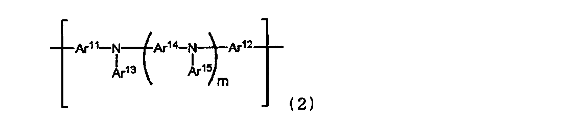
式(2)中、mは0~3の整数を表す。
Ar11及びAr12は、各々独立して、直接結合、置換基を有していてもよい芳香族炭化水素基又は置換基を有していてもよい芳香族複素環基を表す。
Ar13~Ar15は、各々独立に、置換基を有していてもよい芳香族炭化水素基又は置換基を有していてもよい芳香族複素環基を表す。
m個のAr14同士及びAr15同士は、各々、同じでもよく、異なっていてもよい。
但し、Ar11及びAr12が同時に直接結合であることはない。
Ar11及びAr12は、各々独立して、直接結合、置換基を有していてもよい芳香族炭化水素基又は置換基を有していてもよい芳香族複素環基を表す。
Ar13~Ar15は、各々独立に、置換基を有していてもよい芳香族炭化水素基又は置換基を有していてもよい芳香族複素環基を表す。
m個のAr14同士及びAr15同士は、各々、同じでもよく、異なっていてもよい。
但し、Ar11及びAr12が同時に直接結合であることはない。
[2] 前記230℃において互いに側鎖の炭素原子に結合する基が、下記式(1A)~(1I)のいずれかで表される基である[1]に記載の有機フォトダイオード。
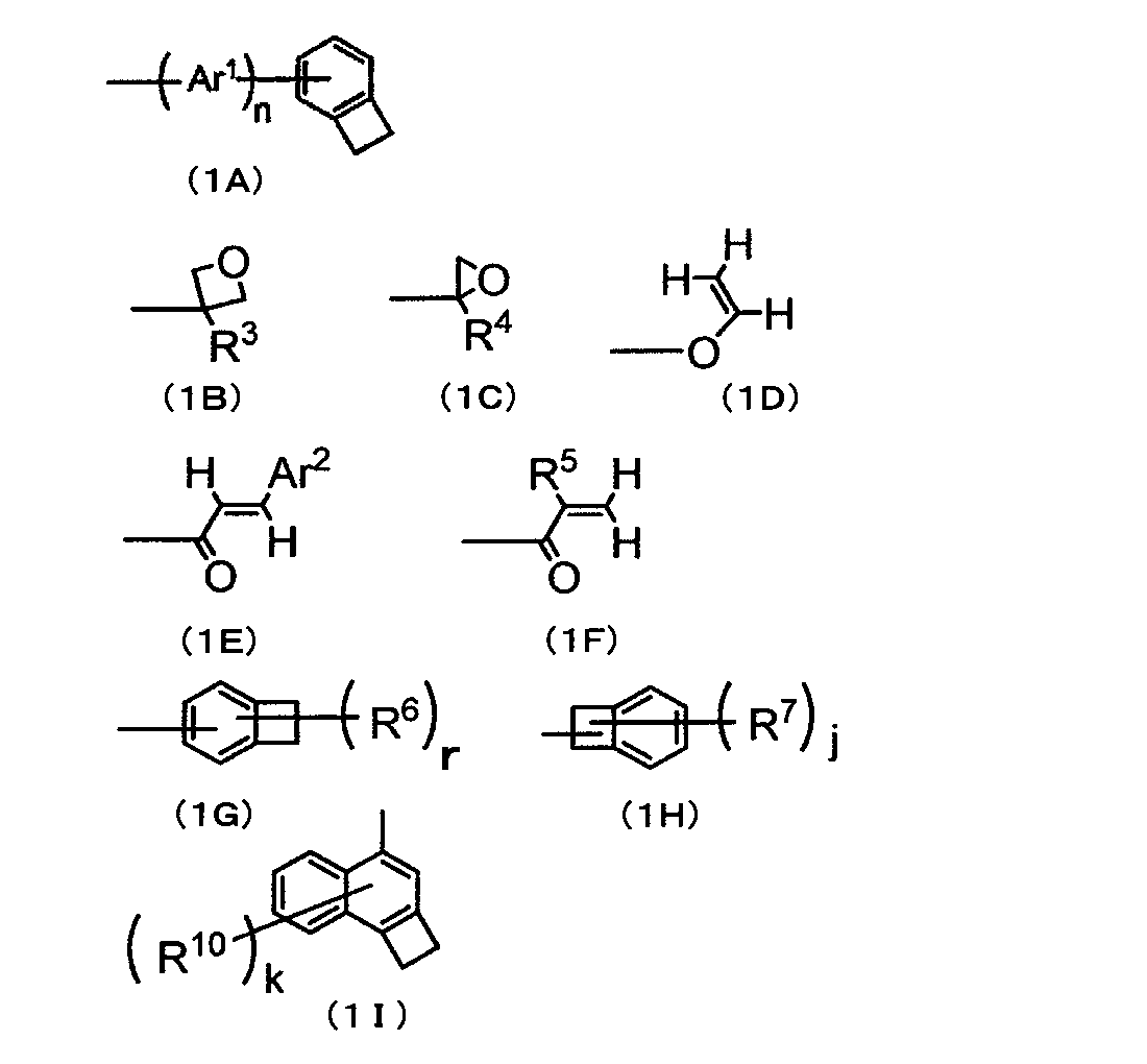
式(1A)中、Ar1は、置換基を有していてもよい芳香族炭化水素基又は置換基を有していてもよい芳香族複素環基を表す。
nは1~6の整数を表す。
n個のAr1は、同じでもよく、異なっていてもよく、式(1A)中のベンゾシクロブテン環は、置換基を有していてもよい。該置換基同士が、互いに結合して環を形成してもよい。
式(1B)~(1I)中、R3~R5は、水素原子又はアルキル基を表す。
R6、R7、R10は、水素原子、アルキル基又はアルコキシ基を表す。
r,jは1~5の整数、kは1~7の整数を表す。
rが2以上のとき、複数のR6は同じであっても異なっていてもよく、隣接するR6同士が結合して環を形成してもよい。
jが2以上のとき、複数のR7は同じであっても異なっていてもよく、隣接するR7同士が結合して環を形成してもよい。
kが2以上のとき、複数のR10は同じであっても異なっていてもよい。
Ar2は、置換基を有していてもよい芳香族炭化水素基又は置換基を有していてもよい芳香族複素環基を表す。
nは1~6の整数を表す。
n個のAr1は、同じでもよく、異なっていてもよく、式(1A)中のベンゾシクロブテン環は、置換基を有していてもよい。該置換基同士が、互いに結合して環を形成してもよい。
式(1B)~(1I)中、R3~R5は、水素原子又はアルキル基を表す。
R6、R7、R10は、水素原子、アルキル基又はアルコキシ基を表す。
r,jは1~5の整数、kは1~7の整数を表す。
rが2以上のとき、複数のR6は同じであっても異なっていてもよく、隣接するR6同士が結合して環を形成してもよい。
jが2以上のとき、複数のR7は同じであっても異なっていてもよく、隣接するR7同士が結合して環を形成してもよい。
kが2以上のとき、複数のR10は同じであっても異なっていてもよい。
Ar2は、置換基を有していてもよい芳香族炭化水素基又は置換基を有していてもよい芳香族複素環基を表す。
[3] 前記230℃において互いに側鎖の炭素原子に結合する基が、開環して重合する基である[1]または[2]に記載の有機フォトダイオード。
[4] 前記n型半導体が下記式(4)で表される[1]~[3]のいずれかに記載の有機フォトダイオード。

式(4)中、Dは多環芳香族を有するドナー部位を表す。Aはマロノニトリル基を有するアクセプター部位を表す。
[5] 前記n型半導体が下記式(5)で表される[1]~[4]のいずれかに記載の有機フォトダイオード。

式(5)中、Ar41はそれぞれ独立に下記式(5a-1)~(5g-1)で表される。
Ar42はそれぞれ独立に下記式(5a-2)~(5d-2)で表される。
Ar43はそれぞれ独立に下記式(5a-3)~(5d-3)で表される。
Ar42はそれぞれ独立に下記式(5a-2)~(5d-2)で表される。
Ar43はそれぞれ独立に下記式(5a-3)~(5d-3)で表される。
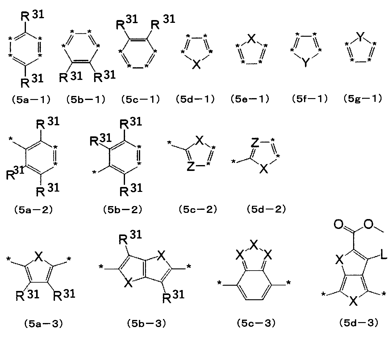
上記式(5a-1)~(5g-1),(5a-2)~(5d-2),(5a-3)~(5d-3)中、*は結合部位を表す。
XはC=O、O、S、又はSeを表す。
YはCR31R31、SiR31R31、GeR31R31、NR31、又はC=Oを表す。
ZはCR31、又はNを表す。
LはR31、又はハロゲン原子を表す。
R31はそれぞれ独立に、水素原子、分岐を有していてもよい炭素数1~30のアルキル基、分岐を有していてもよい炭素数1~30のアルコキシ基、或いは分岐を有していてもよい炭素数1~30のアルキル基及び/又は分岐を有していてもよい炭素数1~30のアルコキシ基で置換されていてもよいフェニル基を表す。
Aはマロノニトリル基を有するアクセプター部位を表す。
x1は0又は1、x2は1~6の整数、x3は0又は1をそれぞれ表す。
式(5)において、式(5f-1)と式(5g-1)とが隣接することはない。
XはC=O、O、S、又はSeを表す。
YはCR31R31、SiR31R31、GeR31R31、NR31、又はC=Oを表す。
ZはCR31、又はNを表す。
LはR31、又はハロゲン原子を表す。
R31はそれぞれ独立に、水素原子、分岐を有していてもよい炭素数1~30のアルキル基、分岐を有していてもよい炭素数1~30のアルコキシ基、或いは分岐を有していてもよい炭素数1~30のアルキル基及び/又は分岐を有していてもよい炭素数1~30のアルコキシ基で置換されていてもよいフェニル基を表す。
Aはマロノニトリル基を有するアクセプター部位を表す。
x1は0又は1、x2は1~6の整数、x3は0又は1をそれぞれ表す。
式(5)において、式(5f-1)と式(5g-1)とが隣接することはない。
[6] 前記Aのマロノニトリル基を有するアクセプター部位が、下記式(5A)~(5C)のいずれかで表される[4]又は[5]に記載の有機フォトダイオード。
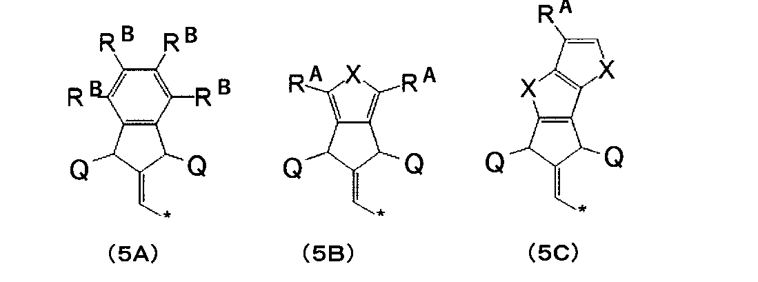
上記式(5A)~(5C)中、*は結合部位を表す。
Qはマロノニトリル基もしくはO=を表す。Qの少なくとも一方はマロノニトリル基である。
XはC=O、O、S、又はSeを表す。
RAはそれぞれ独立に、水素原子、ハロゲン原子、分岐を有していてもよい炭素数1~30のアルキル基、分岐を有していてもよい炭素数1~30のアルコキシ基、或いは分岐を有していてもよい炭素数1~30のアルキル基及び/又は分岐を有していてもよい炭素数1~30のアルコキシ基で置換されていてもよいフェニル基を表す。
RBはRAと同義であるか、或いは隣接するRB同士で芳香族6員環を形成する。
Qはマロノニトリル基もしくはO=を表す。Qの少なくとも一方はマロノニトリル基である。
XはC=O、O、S、又はSeを表す。
RAはそれぞれ独立に、水素原子、ハロゲン原子、分岐を有していてもよい炭素数1~30のアルキル基、分岐を有していてもよい炭素数1~30のアルコキシ基、或いは分岐を有していてもよい炭素数1~30のアルキル基及び/又は分岐を有していてもよい炭素数1~30のアルコキシ基で置換されていてもよいフェニル基を表す。
RBはRAと同義であるか、或いは隣接するRB同士で芳香族6員環を形成する。
[7] 前記高分子化合物が、部分構造としてフルオレン環由来の1価又は2価以上の基を含む[1]~[6]のいずれかに記載の有機フォトダイオード。
[8] 前記高分子化合物の重量平均分子量(Mw)が20000以上であり、分散度(Mw/Mn)が2.5以下である(但し、Mnは数平均分子量を表す。)[1]~[7]のいずれかに記載の有機フォトダイオード。
[9] 前記高分子化合物が、下記式(3)で表される繰り返し単位を含む[1]~[8]のいずれかに記載の有機フォトダイオード。

式(3)中、pは1以上、6以下の整数を表し、qは0以上、3以下の整数を表す。
Ar21及びAr22は、各々独立して、直接結合、置換基を有していてもよい芳香族炭化水素基又は置換基を有していてもよい芳香族複素環基を表す。
Ar23~Ar27は、各々独立に、置換基を有していてもよい芳香族炭化水素基又は置換基を有していてもよい芳香族複素環基を表す。
R1は、水素原子、置換基を有していてもよい炭素数1~24のアルキル基、置換基を有していてもよい炭素数1~24のアルコキシ基、置換基を有してもよい芳香族炭化水素基又は置換基を有してもよい芳香族複素環基を表す。
p個のAr27は、同じでもよく、また異なっていてもよい。q個のAr24同士及びAr25同士は、各々、同じでもよく、異なっていてもよい。Ar21及びAr22が同時に直接結合であることはない。
Ar21及びAr22は、各々独立して、直接結合、置換基を有していてもよい芳香族炭化水素基又は置換基を有していてもよい芳香族複素環基を表す。
Ar23~Ar27は、各々独立に、置換基を有していてもよい芳香族炭化水素基又は置換基を有していてもよい芳香族複素環基を表す。
R1は、水素原子、置換基を有していてもよい炭素数1~24のアルキル基、置換基を有していてもよい炭素数1~24のアルコキシ基、置換基を有してもよい芳香族炭化水素基又は置換基を有してもよい芳香族複素環基を表す。
p個のAr27は、同じでもよく、また異なっていてもよい。q個のAr24同士及びAr25同士は、各々、同じでもよく、異なっていてもよい。Ar21及びAr22が同時に直接結合であることはない。
[10] 前記高分子化合物が、前記式(1)で表される基を、分子量1000あたり0.01個以上、3個以下有する[1]~[9]のいずれかに記載の有機フォトダイオード。
[11] 前記n型半導体において、フラーレン骨格を有するn型半導体の割合が、フラーレン骨格を有さないn型半導体に対して10重量%以下である[1]~[10]のいずれかに記載の有機フォトダイオード。
[12] 前記n型半導体において、フラーレン骨格を有するものが実質的に含まれていない[1]~[11]のいずれかに記載の有機フォトダイオード。
[13] [1]~[12]のいずれかに記載の有機フォトダイオードを含む赤外線CMOSセンサー。
本発明によれば、光電変換効率が高く、しかも暗電流値の低い有機フォトダイオードを実現することができる。本発明の有機フォトダイオードを用いて高性能の赤外線CMOSセンサーを提供することができる。
以下に本発明を実施するための最良の形態を詳細に説明する。以下に記載する構成要件の説明は、本発明の実施態様の代表例であり、本発明はこれらの内容に限定されるものではない。
〔有機フォトダイオード〕
本発明の有機フォトダイオードは、第1電極、正孔輸送層、光電変換層、及び第2電極をこの順に含んでなる有機フォトダイオードであって、該光電変換層がp型半導体とn型半導体を含んでなり、該正孔輸送層が、下記式(2)で表される繰り返し単位を含む高分子化合物を含有し、該高分子化合物が、該高分子化合物間において230℃において互いに側鎖の炭素原子に結合する基を有することを特徴とする。
以下において、本発明に係る正孔輸送層も含まれる、下記式(2)で表される繰り返し単位を含む高分子化合物であって、該高分子化合物間において230℃において互いに側鎖の炭素原子に結合する基を有する高分子化合物を「本発明の正孔輸送性ポリマー」と称す場合がある。
本発明の有機フォトダイオードは、第1電極、正孔輸送層、光電変換層、及び第2電極をこの順に含んでなる有機フォトダイオードであって、該光電変換層がp型半導体とn型半導体を含んでなり、該正孔輸送層が、下記式(2)で表される繰り返し単位を含む高分子化合物を含有し、該高分子化合物が、該高分子化合物間において230℃において互いに側鎖の炭素原子に結合する基を有することを特徴とする。
以下において、本発明に係る正孔輸送層も含まれる、下記式(2)で表される繰り返し単位を含む高分子化合物であって、該高分子化合物間において230℃において互いに側鎖の炭素原子に結合する基を有する高分子化合物を「本発明の正孔輸送性ポリマー」と称す場合がある。
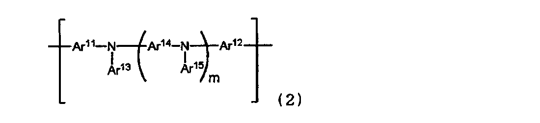
式(2)中、mは0~3の整数を表す。
Ar11及びAr12は、各々独立して、直接結合、置換基を有していてもよい芳香族炭化水素基又は置換基を有していてもよい芳香族複素環基を表す。
Ar13~Ar15は、各々独立に、置換基を有していてもよい芳香族炭化水素基又は置換基を有していてもよい芳香族複素環基を表す。
m個のAr14同士及びAr15同士は、各々、同じでもよく、異なっていてもよい。
但し、Ar11及びAr12が同時に直接結合であることはない。
Ar11及びAr12は、各々独立して、直接結合、置換基を有していてもよい芳香族炭化水素基又は置換基を有していてもよい芳香族複素環基を表す。
Ar13~Ar15は、各々独立に、置換基を有していてもよい芳香族炭化水素基又は置換基を有していてもよい芳香族複素環基を表す。
m個のAr14同士及びAr15同士は、各々、同じでもよく、異なっていてもよい。
但し、Ar11及びAr12が同時に直接結合であることはない。
図1は、本発明の有機フォトダイオードの一例を示す模式的断面図である。この有機フォトダイオード10は、第1電極11、正孔輸送層12、光電変換層13、電子輸送層14、及び下部電極としての第2電極15がこの順で積層されている。正孔輸送層12、光電変換層13及び電子輸送層14で有機光電膜20を形成する。通常、第1電極11の正孔輸送層12とは反対側には基板が設けられる。本発明に係る正孔輸送層を、基板上に形成された第1電極上に設けると、基板の平滑性が正孔輸送層側に影響し、均一な層となるため好ましい。
<正孔輸送性ポリマー>
本発明の有機フォトダイオードにおける正孔輸送層に用いる、前記式(2)で表される繰り返し単位を有する高分子化合物であって、該高分子化合物間において230℃において互いに側鎖の炭素原子に結合する基(以下、この基を単に「230℃において互いに側鎖の炭素原子に結合する基」と称す場合がある。)を有する本発明の正孔輸送性ポリマーについて説明する。
本発明の有機フォトダイオードにおける正孔輸送層に用いる、前記式(2)で表される繰り返し単位を有する高分子化合物であって、該高分子化合物間において230℃において互いに側鎖の炭素原子に結合する基(以下、この基を単に「230℃において互いに側鎖の炭素原子に結合する基」と称す場合がある。)を有する本発明の正孔輸送性ポリマーについて説明する。
本発明の正孔輸送性ポリマーが有する230℃において互いに側鎖の炭素原子に結合する基としては、特に制限はないが、凝集を防ぐよう、重合後主鎖同士が適度に離れるようになるものが望ましいことから、主鎖と架橋性基との間に芳香族炭化水素基又は芳香族複素環基を有するものや、以下の式(1A)~(1I)のいずれかで表される基が挙げられる。

式(1A)中、Ar1は、置換基を有していてもよい芳香族炭化水素基又は置換基を有していてもよい芳香族複素環基を表す。
nは1~6の整数を表す。
n個のAr1は、同じでもよく、異なっていてもよく、式(1A)中のベンゾシクロブテン環は、置換基を有していてもよい。該置換基同士が、互いに結合して環を形成してもよい。
式(1B)~(1I)中、R3~R5は、水素原子又はアルキル基を表す。
R6、R7、R10は、水素原子、アルキル基又はアルコキシ基を表す。
r,jは1~5の整数、kは1~7の整数を表す。
rが2以上のとき、複数のR6は同じであっても異なっていてもよく、隣接するR6同士が結合して環を形成してもよい。
jが2以上のとき、複数のR7は同じであっても異なっていてもよく、隣接するR7同士が結合して環を形成してもよい。
kが2以上のとき、複数のR10は同じであっても異なっていてもよい。
Ar2は、置換基を有していてもよい芳香族炭化水素基又は置換基を有していてもよい芳香族複素環基を表す。
nは1~6の整数を表す。
n個のAr1は、同じでもよく、異なっていてもよく、式(1A)中のベンゾシクロブテン環は、置換基を有していてもよい。該置換基同士が、互いに結合して環を形成してもよい。
式(1B)~(1I)中、R3~R5は、水素原子又はアルキル基を表す。
R6、R7、R10は、水素原子、アルキル基又はアルコキシ基を表す。
r,jは1~5の整数、kは1~7の整数を表す。
rが2以上のとき、複数のR6は同じであっても異なっていてもよく、隣接するR6同士が結合して環を形成してもよい。
jが2以上のとき、複数のR7は同じであっても異なっていてもよく、隣接するR7同士が結合して環を形成してもよい。
kが2以上のとき、複数のR10は同じであっても異なっていてもよい。
Ar2は、置換基を有していてもよい芳香族炭化水素基又は置換基を有していてもよい芳香族複素環基を表す。
ここで、「230℃において互いに側鎖の炭素原子に結合する」とは、開環して重合を行う温度である230℃において、本発明の正孔輸送性ポリマーが重合することで不溶化してそのあとのプロセスで塗布による積層が可能であることにつながり、塗布プロセスを採用する点で効果的である。この意味でより好ましくは、より低温である200℃において互いに側鎖の炭素原子に結合することができる基であることがより好ましい。
本発明において、230℃において互いに側鎖の炭素原子に結合する基があるかどうかは、当業者であれば基の種類により容易に判別できるが、全体構造から判別が難しい場合には、以下のようにして確認することができる。
即ち、当該高分子化合物をトルエンに適量溶解させ、これを基材に塗布したのち、230℃で1時間加熱乾燥して、膜厚25nmから100nmの膜を得、得られた膜が常温のトルエン中に保持しても、実質的に溶解しないことにより確認することができる。この場合、トルエンに実質的に溶解せず膜厚がほとんど減少しないことを、断面SEM観察等で確認すればよい。
本発明において、230℃において互いに側鎖の炭素原子に結合する基があるかどうかは、当業者であれば基の種類により容易に判別できるが、全体構造から判別が難しい場合には、以下のようにして確認することができる。
即ち、当該高分子化合物をトルエンに適量溶解させ、これを基材に塗布したのち、230℃で1時間加熱乾燥して、膜厚25nmから100nmの膜を得、得られた膜が常温のトルエン中に保持しても、実質的に溶解しないことにより確認することができる。この場合、トルエンに実質的に溶解せず膜厚がほとんど減少しないことを、断面SEM観察等で確認すればよい。
本発明の正孔輸送性ポリマーが有する230℃において互いに側鎖の炭素原子に結合する基は、特に開環して前記高分子化合物同士が重合する基であることが、不溶化してそのあとのプロセスにおける積層塗布の観点から好ましい。従って、上記式(1A)~(1I)のいずれかで表される基が好ましく、より好ましくは、シクロブテン基を有する上記式(1A)、(1G)、(1H)、(1I)で表される基である。
[1.式(1A)で表される基を有する正孔輸送性ポリマー]
本発明の正孔輸送性ポリマーの代表例として、前記式(1A)で表される基を有し、前記式(2)で表される繰り返し単位を含む正孔輸送性ポリマー(以下、「本発明の正孔輸送性ポリマー(1A)」と称す場合がある。)の前記式(1A)で表される基について説明する。
本発明の正孔輸送性ポリマーの代表例として、前記式(1A)で表される基を有し、前記式(2)で表される繰り返し単位を含む正孔輸送性ポリマー(以下、「本発明の正孔輸送性ポリマー(1A)」と称す場合がある。)の前記式(1A)で表される基について説明する。
本発明の正孔輸送性ポリマー(1A)は、主鎖中の炭素原子に、1~6個の芳香族炭化水素基又は芳香族複素環基であるAr1を介して、ベンゾシクロブテン環が存在する。
本発明の正孔輸送性ポリマー(1A)は、主鎖と架橋性基との間に、1~6個の芳香族炭化水素基又は芳香族複素環基を介することから、主鎖同士が適度に離れており、凝集などが起こらず、更に、架橋した主鎖間での正孔移動も促進される。また、主鎖と架橋性基との間が剛直な構造であることから、耐熱性にも優れる。
本発明の正孔輸送性ポリマー(1A)は、主鎖に存在するsp3混成軌道の中心となる炭素原子に、1~6個の芳香族炭化水素基又は芳香族複素環基を介して、ベンゾシクロブテン環が存在することが好ましい。
sp3混成軌道の中心となる炭素原子は、π共役系に関与しないため、sp3混成軌道の中心となる炭素原子に結合する側鎖である架橋性基は正孔輸送の妨げとなりにくい。このため、正孔輸送性ポリマー及び正孔輸送性ポリマーを架橋して得られる網目状ポリマーは正孔輸送性がより向上する。
さらに、ポリマーの主鎖に存在するsp3混成軌道の中心である原子は、sp2混成軌道の中心である原子に比べ、周りの結合の回転が起こりやすい。このため、正孔輸送性ポリマーにおける架橋性基は効率よく反応するため、架橋性基の数が少なくても、又は、架橋反応の条件が穏和であっても有機溶剤に対して難溶とすることができる。
式(1A)中のベンゾシクロブテン環が、Ar1以外に有していてもよい置換基としては、後述の[置換基群Z]の項に記載のものが挙げられる。置換基による立体障害や、置換基の電子的効果による架橋反応時の影響が小さい点で、式(1A)中のベンゾシクロブテン環は、Ar1以外に置換基を有さないことが好ましい。
[1-1.Ar1]
Ar1は、置換基を有していてもよい芳香族炭化水素基、置換基を有していてもよい芳香族複素環基を表す。
Ar1は、置換基を有していてもよい芳香族炭化水素基、置換基を有していてもよい芳香族複素環基を表す。
Ar1の芳香族炭化水素基としては、例えば、ベンゼン環、ナフタレン環、アントラセン環、フェナントレン環、ペリレン環、テトラセン環、ピレン環、ベンズピレン環、クリセン環、トリフェニレン環、アセナフテン環、フルオランテン環、フルオレン環などの、6員環の単環又は2~5縮合環の1価以上の基が挙げられる。
Ar1の芳香族複素環基としては、例えば、フラン環、ベンゾフラン環、チオフェン環、ベンゾチオフェン環、ピロール環、ピラゾール環、イミダゾール環、オキサジアゾール環、インドール環、カルバゾール環、ピロロイミダゾール環、ピロロピラゾール環、ピロロピロール環、チエノピロール環、チエノチオフェン環、フロピロール環、フロフラン環、チエノフラン環、ベンゾイソオキサゾール環、ベンゾイソチアゾール環、ベンゾイミダゾール環、ピリジン環、ピラジン環、ピリダジン環、ピリミジン環、トリアジン環、キノリン環、イソキノリン環、シノリン環、キノキサリン環、フェナントリジン環、ベンゾイミダゾール環、ペリミジン環、キナゾリン環、キナゾリノン環、アズレン環などの、5又は6員環の単環又は2~4縮合環の1価以上の基が挙げられる。
正孔輸送性が優れる点、耐久性に優れる点から、Ar1は、ベンゼン環、ナフタレン環、アントラセン環、フェナントレン環、からなる群より選ばれる環由来の基が好ましく、ベンゼン環由来の基、すなわち、フェニレン基であることが最も好ましい。
Ar1の芳香族炭化水素基、芳香族複素環基が有してもよい置換基としては、特に制限はないが、例えば、下記置換基群Zから選ばれる基が挙げられる。この置換基としては、アルキル基、アルコキシ基、芳香族炭化水素基、芳香族複素環基が好ましい。
正孔輸送性が優れる点、耐久性に優れる点から、Ar1の炭素数は、置換基を含めて、通常3以上、好ましくは5以上、さらに好ましくは6以上であり、通常36以下、好ましくは24以下、さらに好ましくは12以下である。
[置換基群Z]
例えばメチル基、エチル基、n-プロピル基、i-プロピル基、n-ブチル基、i-ブチル基、sec-ブチル基、tert-ブチル基、n-ヘキシル基、シクロヘキシル基、ドデシル基などの、炭素数が通常1以上であり、通常24以下、好ましくは12以下である、直鎖、分岐、又は環状のアルキル基;
例えばビニル基等の、炭素数が通常2以上であり、通常24以下、好ましくは12以下であるアルケニル基;
例えばエチニル基等の、炭素数が通常2以上であり、通常24以下、好ましくは12以下であるアルキニル基;
例えばメトキシ基、エトキシ基等の、炭素数が通常1以上であり、通常24以下、好ましくは12以下であるアルコキシ基;
例えばフェノキシ基、ナフトキシ基、ピリジルオキシ基等の、炭素数が通常4以上、好ましくは5以上であり、通常36以下、好ましくは24以下であるアリールオキシ基;
例えばメトキシカルボニル基、エトキシカルボニル基等の、炭素数が通常2以上であり、通常24以下、好ましくは12以下であるアルコキシカルボニル基;
例えばジメチルアミノ基、ジエチルアミノ基等の、炭素数が通常2以上であり、通常24以下、好ましくは12以下であるジアルキルアミノ基;
例えばジフェニルアミノ基、ジトリルアミノ基、N-カルバゾリル基等の、炭素数が通常10以上、好ましくは12以上であり、通常36以下、好ましくは24以下のジアリールアミノ基;
例えばフェニルメチルアミノ基等の、炭素数が通常7以上であり、通常36以下、好ましくは24以下であるアリールアルキルアミノ基;
例えばアセチル基、ベンゾイル基等の、炭素数が通常2以上であり、通常24以下、好ましくは12以下であるアシル基;
例えばフッ素原子、塩素原子等のハロゲン原子;
例えばトリフルオロメチル基等の、炭素数が通常1以上であり、通常12以下、好ましくは6以下のハロアルキル基;
例えばメチルチオ基、エチルチオ基等の、炭素数が通常1以上であり、通常24以下、好ましくは12以下のアルキルチオ基;
例えばフェニルチオ基、ナフチルチオ基、ピリジルチオ基等の、炭素数が通常4以上、好ましくは5以上であり、通常36以下、好ましくは24以下であるアリールチオ基;
例えばトリメチルシリル基、トリフェニルシリル基等の、炭素数が通常2以上、好ましくは3以上であり、通常36以下、好ましくは24以下であるシリル基;
例えばトリメチルシロキシ基、トリフェニルシロキシ基等の、炭素数が通常2以上、好ましくは3以上であり、通常36以下、好ましくは24以下であるシロキシ基;
シアノ基;
例えばフェニル基、ナフチル基等の、炭素数が通常6以上であり、通常36以下、好ましくは24以下である芳香族炭化水素基;
例えばチエニル基、ピリジル基等の、炭素数が通常3以上、好ましくは4以上であり、通常36以下、好ましくは24以下である芳香族複素環基
例えばメチル基、エチル基、n-プロピル基、i-プロピル基、n-ブチル基、i-ブチル基、sec-ブチル基、tert-ブチル基、n-ヘキシル基、シクロヘキシル基、ドデシル基などの、炭素数が通常1以上であり、通常24以下、好ましくは12以下である、直鎖、分岐、又は環状のアルキル基;
例えばビニル基等の、炭素数が通常2以上であり、通常24以下、好ましくは12以下であるアルケニル基;
例えばエチニル基等の、炭素数が通常2以上であり、通常24以下、好ましくは12以下であるアルキニル基;
例えばメトキシ基、エトキシ基等の、炭素数が通常1以上であり、通常24以下、好ましくは12以下であるアルコキシ基;
例えばフェノキシ基、ナフトキシ基、ピリジルオキシ基等の、炭素数が通常4以上、好ましくは5以上であり、通常36以下、好ましくは24以下であるアリールオキシ基;
例えばメトキシカルボニル基、エトキシカルボニル基等の、炭素数が通常2以上であり、通常24以下、好ましくは12以下であるアルコキシカルボニル基;
例えばジメチルアミノ基、ジエチルアミノ基等の、炭素数が通常2以上であり、通常24以下、好ましくは12以下であるジアルキルアミノ基;
例えばジフェニルアミノ基、ジトリルアミノ基、N-カルバゾリル基等の、炭素数が通常10以上、好ましくは12以上であり、通常36以下、好ましくは24以下のジアリールアミノ基;
例えばフェニルメチルアミノ基等の、炭素数が通常7以上であり、通常36以下、好ましくは24以下であるアリールアルキルアミノ基;
例えばアセチル基、ベンゾイル基等の、炭素数が通常2以上であり、通常24以下、好ましくは12以下であるアシル基;
例えばフッ素原子、塩素原子等のハロゲン原子;
例えばトリフルオロメチル基等の、炭素数が通常1以上であり、通常12以下、好ましくは6以下のハロアルキル基;
例えばメチルチオ基、エチルチオ基等の、炭素数が通常1以上であり、通常24以下、好ましくは12以下のアルキルチオ基;
例えばフェニルチオ基、ナフチルチオ基、ピリジルチオ基等の、炭素数が通常4以上、好ましくは5以上であり、通常36以下、好ましくは24以下であるアリールチオ基;
例えばトリメチルシリル基、トリフェニルシリル基等の、炭素数が通常2以上、好ましくは3以上であり、通常36以下、好ましくは24以下であるシリル基;
例えばトリメチルシロキシ基、トリフェニルシロキシ基等の、炭素数が通常2以上、好ましくは3以上であり、通常36以下、好ましくは24以下であるシロキシ基;
シアノ基;
例えばフェニル基、ナフチル基等の、炭素数が通常6以上であり、通常36以下、好ましくは24以下である芳香族炭化水素基;
例えばチエニル基、ピリジル基等の、炭素数が通常3以上、好ましくは4以上であり、通常36以下、好ましくは24以下である芳香族複素環基
以上の置換基群Zの中でも、溶解性の点から、炭素数1~12のアルキル基及び炭素数1~12のアルコキシ基が好ましい。
また、上記各置換基がさらに置換基を有していてもよく、その例としては置換基群Zの項に例示した基から選択される。
また、上記各置換基がさらに置換基を有していてもよく、その例としては置換基群Zの項に例示した基から選択される。
[1-2.n]
nは1以上、6以下の整数を表す。架橋反応が進行しやすい点、架橋反応後に主鎖が凝集したり、離れすぎたりすることがなく正孔輸送性に優れる点で、nは1以上、3以下の整数であることが好ましい。nが2以上の場合、n個のAr1は、同じでもよく、異なっていてもよい。
nは1以上、6以下の整数を表す。架橋反応が進行しやすい点、架橋反応後に主鎖が凝集したり、離れすぎたりすることがなく正孔輸送性に優れる点で、nは1以上、3以下の整数であることが好ましい。nが2以上の場合、n個のAr1は、同じでもよく、異なっていてもよい。
[2.式(1B)~式(1I)で表される基]
本発明の正孔輸送性ポリマーは、式(1A)で表される基の代りに、前記式(1B)~式(1I)のいずれかで表される基を有するものであってもよく、式(1A)で表される基と、式(1B)~式(1I)のいずれかで表される基とを有するものであってもよい。
本発明の正孔輸送性ポリマーは、式(1A)で表される基の代りに、前記式(1B)~式(1I)のいずれかで表される基を有するものであってもよく、式(1A)で表される基と、式(1B)~式(1I)のいずれかで表される基とを有するものであってもよい。
前記式(1B),(1C),(1F)~(1I)中のR3~R7、R10のアルキル基としては、通常、炭素数が6以下である直鎖又は分岐の鎖状アルキル基が好ましく、例えばメチル基、エチル基、n-プロピル基、2-プロピル基、n-ブチル基、イソブチル基等である。より好ましくはメチル基又はエチル基である。R3~R7、R10の炭素数が6以下であれば、架橋反応を立体的に阻害することもなく、形成される膜の不溶化が起こりやすい傾向にある。
R6、R7、R10のアルコキシ基としては、通常、炭素数が6以下である直鎖又は分岐の鎖状アルコキシ基が好ましく、例えばメトキシ基、エトキシ基、n-プロポキシ基、2-プロポキシ基、n-ブトキシ基等である。より好ましくはメトキシ基、エトキシ基である。R6、R7、R10の炭素数が6以下であれば、架橋反応を立体的に阻害することもなく、形成される膜の不溶化が起こりやすい傾向にある。
式(1E)中のAr2の置換基を有していてもよい芳香族炭化水素基としては、例えば、1個の遊離原子価を有する、ベンゼン環、ナフタレン環等の6員環の単環又は2~5縮合環が挙げられる。特に1個の遊離原子価を有するベンゼン環が好ましい。Ar2は、置換基を有していてもよい芳香族炭化水素基を2以上結合させた基であっても良い。このような基としては、ビフェニレン基、ターフェニレン基等が挙げられ、4,4’-ビフェニレン基が好ましい。
Ar2が有していてもよい置換基は前述の[置換基群Z]と同様である。
上記式(1A)~(1I)に示される架橋性基のうち、エポキシ基、オキセタン基等の環状エーテル基、ビニルエーテル基等のカチオン重合によって架橋反応する基が、反応性が高く、架橋による不溶化が容易な点で好ましい。中でも、カチオン重合の速度を制御しやすい点でオキセタン基がより好ましく、カチオン重合の際に素子の劣化をまねくおそれのあるヒドロキシル基が生成しにくい点でビニルエーテル基が好ましい。
シンナモイル基などアリールビニルカルボニル基、1価の遊離原子価を有するベンゾシクロブテン環、1価の遊離原子価を有する1,2-ジヒドロシクロブタ〔a〕ナフタレン環等の環化付加反応する基が、素子の電気化学的安定性をさらに向上させる点で好ましい。
これらの架橋性基の中でも、架橋後の構造が特に安定な点で、1価の遊離原子価を有する芳香族環に縮環したシクロブテン環、1価の遊離原子価を有する1,2-ジヒドロシクロブタ〔a〕ナフタレン環を含む基が好ましい。中でもベンゾシクロブテン環または1価の遊離原子価を有する1,2-ジヒドロシクロブタ〔a〕ナフタレン環が更に好ましく、架橋反応温度が低い点で1価の遊離原子価を有する1,2-ジヒドロシクロブタ〔a〕ナフタレン環が特に好ましい。
[3.式(2)で表される繰り返し単位]
本発明の正孔輸送性ポリマーは、前記式(2)で表される繰り返し単位を含む。本発明の正孔輸送性ポリマーは、主鎖にアミン構造を有し、sp3混成軌道の中心となる窒素原子を有することで、正孔輸送性、電気的耐久性に優れたものとなる。
本発明の正孔輸送性ポリマーは、前記式(2)で表される繰り返し単位を含む。本発明の正孔輸送性ポリマーは、主鎖にアミン構造を有し、sp3混成軌道の中心となる窒素原子を有することで、正孔輸送性、電気的耐久性に優れたものとなる。
[3-1.Ar11~Ar15]
式(2)中、Ar11及びAr12は、各々独立して、直接結合、置換基を有していてもよい芳香族炭化水素基、又は置換基を有していてもよい芳香族複素環基を表す。Ar11及びAr12が同時に直接結合であることはない。Ar13~Ar15は、各々独立に、置換基を有していてもよい芳香族炭化水素基又は置換基を有していてもよい芳香族複素環基を表す。
式(2)中、Ar11及びAr12は、各々独立して、直接結合、置換基を有していてもよい芳香族炭化水素基、又は置換基を有していてもよい芳香族複素環基を表す。Ar11及びAr12が同時に直接結合であることはない。Ar13~Ar15は、各々独立に、置換基を有していてもよい芳香族炭化水素基又は置換基を有していてもよい芳香族複素環基を表す。
Ar11~Ar15の置換基を有していてもよい芳香族炭化水素基としては、例えば、ベンゼン環、ナフタレン環、アントラセン環、フェナントレン環、ペリレン環、テトラセン環、ピレン環、ベンズピレン環、クリセン環、トリフェニレン環、アセナフテン環、フルオランテン環、フルオレン環などの、6員環の単環又は2~5縮合環由来の基が挙げられる。
Ar11~Ar15の置換基を有していてもよい芳香族複素環基としては、例えばフラン環、ベンゾフラン環、チオフェン環、ベンゾチオフェン環、ピロール環、ピラゾール環、イミダゾール環、オキサジアゾール環、インドール環、カルバゾール環、ピロロイミダゾール環、ピロロピラゾール環、ピロロピロール環、チエノピロール環、チエノチオフェン環、フロピロール環、フロフラン環、チエノフラン環、ベンゾイソオキサゾール環、ベンゾイソチアゾール環、ベンゾイミダゾール環、ピリジン環、ピラジン環、ピリダジン環、ピリミジン環、トリアジン環、キノリン環、イソキノリン環、シノリン環、キノキサリン環、フェナントリジン環、ベンゾイミダゾール環、ペリミジン環、キナゾリン環、キナゾリノン環、アズレン環などの、5又は6員環の単環又は2~4縮合環由来の基が挙げられる。
溶剤に対する溶解性及び耐熱性の点から、Ar11~Ar15は、各々独立に、ベンゼン環、ナフタレン環、アントラセン環、フェナントレン環、トリフェニレン環、ピレン環、チオフェン環、ピリジン環、フルオレン環からなる群より選ばれる環由来の基が好ましい。
Ar11~Ar15としては、前記群から選ばれる1種又は2種以上の環を直接結合により連結した基も好ましく、ビフェニル基、ビフェニレン基及びターフェニル基、ターフェニレン基がさらに好ましい。
前記置換基を有していてもよい芳香族炭化水素基及び置換基を有していてもよい芳香族複素環基が有していてもよい置換基としては、前述の[置換基群Z]に記載の基が挙げられる。
正孔輸送性に優れる点から、Ar11~Ar15の炭素数は、置換基を含めて、通常3以上、好ましくは5以上、さらに好ましくは6以上であり、通常72以下、好ましくは48以下、さらに好ましくは25以下である。
[3-2.m]
式(2)におけるmは、0以上、3以下の整数を表す。
式(2)におけるmは、0以上、3以下の整数を表す。
架橋性ポリマーの、有機溶剤に対する溶解性及び成膜性が高められる点で、mは0であることが好ましい。ポリマーの正孔輸送能が向上する点で、mは1以上、3以下であることが好ましい。
mが2以上である場合、前記式(2)で表される繰り返し単位は、2個以上のAr14及びAr15を有することになる。その場合、Ar14同士及びAr15同士は、各々、同じでもよく、異なっていてもよい。Ar14同士、Ar15同士は、各々互いに直接又は連結基を介して結合して環状構造を形成していてもよい。
[4.式(3)で表される繰り返し単位]
本発明の正孔輸送性ポリマーは、正孔輸送性に優れる点、電気的耐久性に優れる点から、下記式(3)で表される繰り返し単位を含むことが好ましい。
本発明の正孔輸送性ポリマーは、正孔輸送性に優れる点、電気的耐久性に優れる点から、下記式(3)で表される繰り返し単位を含むことが好ましい。

式(3)中、pは1以上、6以下の整数を表し、qは0以上、3以下の整数を表す。
Ar21及びAr22は、各々独立して、直接結合、置換基を有していてもよい芳香族炭化水素基又は置換基を有していてもよい芳香族複素環基を表す。
Ar23~Ar27は、各々独立に、置換基を有していてもよい芳香族炭化水素基又は置換基を有していてもよい芳香族複素環基を表す。
R1は、水素原子、置換基を有していてもよい炭素数1~24のアルキル基、置換基を有していてもよい炭素数1~24のアルコキシ基、置換基を有してもよい芳香族炭化水素基又は置換基を有してもよい芳香族複素環基を表す。
p個のAr27は、同じでもよく、また異なっていてもよい。q個のAr24同士及びAr25同士は、各々、同じでもよく、異なっていてもよい。Ar21及びAr22が同時に直接結合であることはない。
Ar21及びAr22は、各々独立して、直接結合、置換基を有していてもよい芳香族炭化水素基又は置換基を有していてもよい芳香族複素環基を表す。
Ar23~Ar27は、各々独立に、置換基を有していてもよい芳香族炭化水素基又は置換基を有していてもよい芳香族複素環基を表す。
R1は、水素原子、置換基を有していてもよい炭素数1~24のアルキル基、置換基を有していてもよい炭素数1~24のアルコキシ基、置換基を有してもよい芳香族炭化水素基又は置換基を有してもよい芳香族複素環基を表す。
p個のAr27は、同じでもよく、また異なっていてもよい。q個のAr24同士及びAr25同士は、各々、同じでもよく、異なっていてもよい。Ar21及びAr22が同時に直接結合であることはない。
[4-1.Ar21~Ar26、q]
式(3)中、Ar21、Ar22は、各々独立して、直接結合、置換基を有していてもよい芳香族炭化水素基、又は置換基を有していてもよい芳香族複素環基を表す。Ar21及びAr22が同時に直接結合であることはない。
式(3)中、Ar21、Ar22は、各々独立して、直接結合、置換基を有していてもよい芳香族炭化水素基、又は置換基を有していてもよい芳香族複素環基を表す。Ar21及びAr22が同時に直接結合であることはない。
Ar23~Ar26は、各々独立に、置換基を有していてもよい芳香族炭化水素基又は置換基を有していてもよい芳香族複素環基を表す。
Ar21~Ar26の具体例、好ましい例は、前述の、Ar11~Ar15と同様である。
式(3)におけるqは、0以上、3以下の整数を表す。ポリマーの、有機溶剤に対する溶解性及び成膜性が高められる点で、qは0であることが好ましい。ポリマーの正孔輸送能が向上する点で、qは1以上、3以下であることが好ましい。
qが2以上である場合、前記式(3)で表される繰り返し単位は、2個以上のAr24及びAr25を有することになる。その場合、Ar24同士及びAr25同士は、各々、同じでもよく、異なっていてもよい。Ar24同士、Ar25同士は、各々互いに直接又は連結基を介して結合して環状構造を形成していてもよい。
[4-2.Ar27、p]
式(3)における(Ar27)pは、sp3混成軌道の中心となる炭素原子とベンゾシクロブテン環に結合する基であり、式(1A)における(Ar1)nである。Ar27は、置換基を有していてもよい芳香族炭化水素基又は置換基を有していてもよい芳香族複素環基を表す。pは0以上、6以下の整数を表す。p個のAr27は、同じでもよく、また異なっていてもよい。Ar27の具体例、好ましい例は、前述の、Ar1と同様である。
式(3)における(Ar27)pは、sp3混成軌道の中心となる炭素原子とベンゾシクロブテン環に結合する基であり、式(1A)における(Ar1)nである。Ar27は、置換基を有していてもよい芳香族炭化水素基又は置換基を有していてもよい芳香族複素環基を表す。pは0以上、6以下の整数を表す。p個のAr27は、同じでもよく、また異なっていてもよい。Ar27の具体例、好ましい例は、前述の、Ar1と同様である。
[4-3.R1]
R1は、水素原子、置換基を有していてもよい炭素数1~24のアルキル基、置換基を有していてもよい炭素数1~24のアルコキシ基、置換基を有してもよい芳香族炭化水素基又は置換基を有してもよい芳香族複素環基を表す。中でも、正孔輸送性に優れる点、架橋反応前の溶解性が高い点から、アルキル基が好ましい。
R1は、水素原子、置換基を有していてもよい炭素数1~24のアルキル基、置換基を有していてもよい炭素数1~24のアルコキシ基、置換基を有してもよい芳香族炭化水素基又は置換基を有してもよい芳香族複素環基を表す。中でも、正孔輸送性に優れる点、架橋反応前の溶解性が高い点から、アルキル基が好ましい。
アルキル基としては、メチル基、エチル基、n-プロピル基、i-プロピル基、n-ブチル基、i-ブチル基、sec-ブチル基、tert-ブチル基、n-ヘキシル基、シクロヘキシル基、ドデシル基などの、炭素数が通常1以上であり、通常24以下、好ましくは12以下である基が好ましい。アルコキシ基としてはメトキシ基、エトキシ基等の、炭素数が通常1以上であり、通常24以下、好ましくは12以下である基が好ましい。有してもよい置換基としては、前述の置換基群Zから選ばれる基が挙げられ、アルキル基、アルコキシ基、芳香族炭化水素基、芳香族複素環基が好ましい。
置換基を有してもよい芳香族炭化水素基、置換基を有してもよい芳香族複素環基である場合の具体例、好ましい例は、前述のAr11~Ar15について記載したものと同様である。
[5.好ましい部分構造]
本発明の正孔輸送性ポリマーは、正孔輸送性に優れる点に加え、架橋反応前の溶解性に優れる点で、部分構造としてフルオレン環由来の1価又は2価以上の基を含むことが好ましい。
本発明の正孔輸送性ポリマーは、正孔輸送性に優れる点に加え、架橋反応前の溶解性に優れる点で、部分構造としてフルオレン環由来の1価又は2価以上の基を含むことが好ましい。
[6.式(1A)~(1I)のいずれかで表される基等の230℃において互いに側鎖の炭素原子に結合する基の数]
本発明においては、本発明の正孔輸送性ポリマーが有する230℃において互いに側鎖の炭素原子に結合する基、好ましくは式(1A)~(1I)のいずれかで表される基の数を、分子量1000あたりの数で表す。ここで、正孔輸送性ポリマーの分子量1000あたりの式(1A)~(1I)のいずれかで表される基等の230℃において互いに側鎖の炭素原子に結合する基の数(以下、「式(1)数/1000」と称す場合がある。)は、正孔輸送性ポリマーからその末端基を除いて、合成時の仕込みモノマーのモル比と、構造式から算出することができる。
本発明においては、本発明の正孔輸送性ポリマーが有する230℃において互いに側鎖の炭素原子に結合する基、好ましくは式(1A)~(1I)のいずれかで表される基の数を、分子量1000あたりの数で表す。ここで、正孔輸送性ポリマーの分子量1000あたりの式(1A)~(1I)のいずれかで表される基等の230℃において互いに側鎖の炭素原子に結合する基の数(以下、「式(1)数/1000」と称す場合がある。)は、正孔輸送性ポリマーからその末端基を除いて、合成時の仕込みモノマーのモル比と、構造式から算出することができる。
例えば、後述の実施例2で用いた式(H1)で表されるポリマー(H1)の場合で説明する。ポリマー(H1)において、末端基を除いた分子量は503.42であり、式(1A)で表される基の数は、1分子当たり平均0.05個である。これを単純比例により計算すると、分子量1000あたりの式(1A)で表される基の数は、0.1個と算出される。
本発明の正孔輸送性ポリマーが有する式(1A)~(1I)のいずれかで表される基の数は、分子量1000あたり、通常3.0個以下、好ましくは2.0個以下、さらに好ましくは1.0個以下、また通常0.01個以上、好ましくは0.05個以上である。
式(1)数/1000が上記上限値を上回ると、クラックによって平坦な膜が得られなかったり、また、架橋密度が大きくなりすぎて、架橋層中に未反応の式(1A)~(1I)のいずれかで表される基が増えて、得られる有機フォトダイオードの寿命に影響を及ぼしたりするおそれがある。式(1)数/1000が上記下限値を下回ると、架橋層の不溶化が不十分となり、湿式成膜法で多層積層構造が形成できないおそれがある。
[7.好ましい分子量分布]
本発明の正孔輸送性ポリマーは、正孔輸送性に優れる点、架橋反応後に有機溶剤に対して難溶となり易い点から、重量平均分子量(Mw)が20000以上であることが好ましく、60000以上であることがさらに好ましい。重量平均分子量(Mw)の上限は、後述の正孔輸送層形成用組成物の濾過性が低下する、正孔輸送層形成用組成物の粘性が高くなりすぎて薄膜の形成が難しくなるといった観点から、通常500000以下、好ましくは200000以下である。
本発明の正孔輸送性ポリマーは、正孔輸送性に優れる点、架橋反応後に有機溶剤に対して難溶となり易い点から、重量平均分子量(Mw)が20000以上であることが好ましく、60000以上であることがさらに好ましい。重量平均分子量(Mw)の上限は、後述の正孔輸送層形成用組成物の濾過性が低下する、正孔輸送層形成用組成物の粘性が高くなりすぎて薄膜の形成が難しくなるといった観点から、通常500000以下、好ましくは200000以下である。
本発明の正孔輸送性ポリマーは、正孔輸送性に優れる点、架橋反応後に有機溶剤に対して難溶となり易い点から、分散度(Mw/Mn)が2.5以下であることが好ましく、2.0以下であることがさらに好ましい。
この重量平均分子量(Mw)及び分散度(Mw/Mn)は、SEC(サイズ排除クロマトグラフィー)測定により決定される。SEC測定では高分子量成分ほど溶出時間が短く、低分子量成分ほど溶出時間が長くなる。分子量既知のポリスチレン(標準試料)の溶出時間から算出した校正曲線を用いて、サンプルの溶出時間を分子量に換算することによって、重量平均分子量が算出される。
[8.具体例]
以下に本発明の正孔輸送性ポリマー(1A)の繰り返し単位の好ましい例を示す。本発明の正孔輸送性ポリマーの繰り返し単位はこれらに限定されるものではない。
以下に本発明の正孔輸送性ポリマー(1A)の繰り返し単位の好ましい例を示す。本発明の正孔輸送性ポリマーの繰り返し単位はこれらに限定されるものではない。
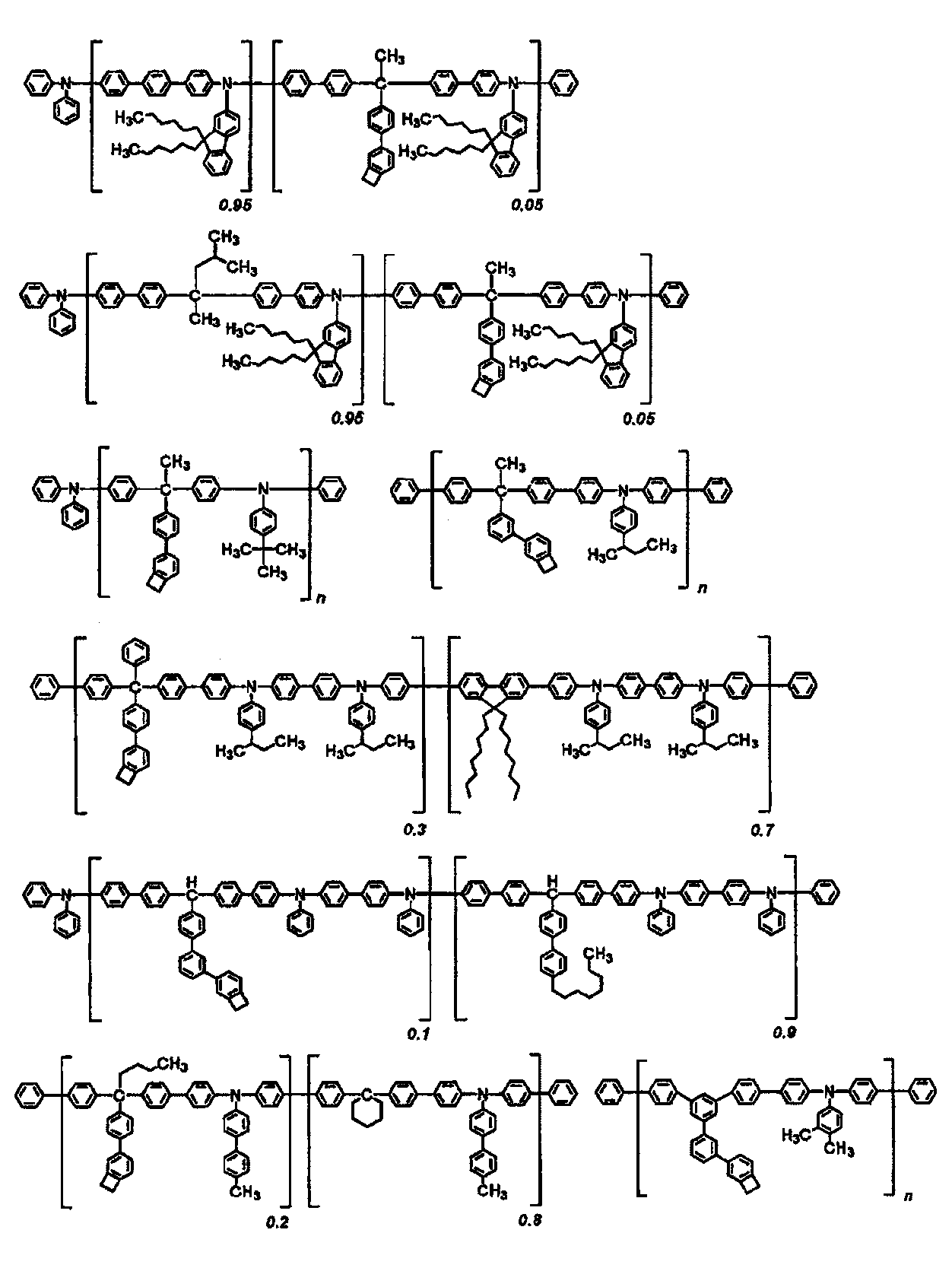
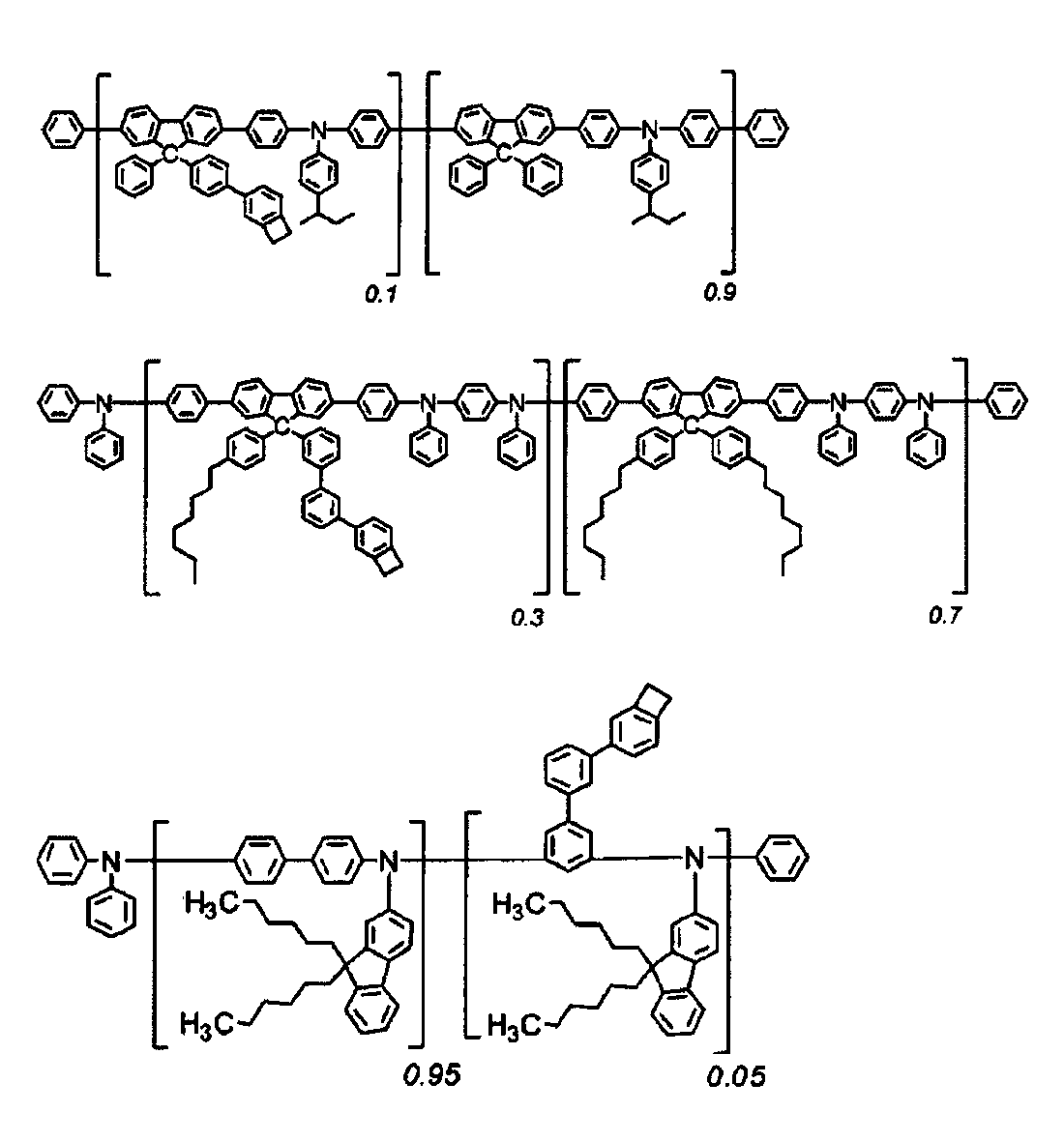
[9.合成方法]
本発明の正孔輸送性ポリマーは、目的とする化合物の構造に応じて原料を選択し、公知の手法を用いて合成することができる。
本発明の正孔輸送性ポリマーは、目的とする化合物の構造に応じて原料を選択し、公知の手法を用いて合成することができる。
式(1A)で表される基を有するモノマーの合成方法としては、公知のカップリング手法が適用可能である。例えば、下記反応式のようにSuzuki反応によって合成される。
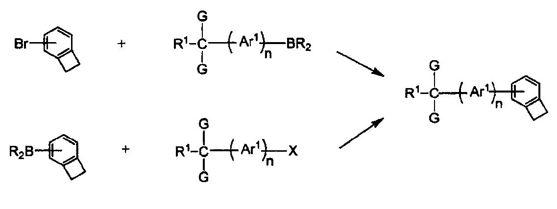
上記反応式中、Gは、ポリマー化の際に反応をする基を表す。BR2はボロン酸基又はボロン酸エステル基を表す。R1は、水素原子、置換基を有していてもよい炭素数1~24のアルキル基、置換基を有していてもよい炭素数1~24のアルコキシ基、置換基を有してもよい芳香族炭化水素基又は置換基を有してもよい芳香族複素環基を表す。Ar1は、置換基を有していてもよい芳香族炭化水素基又は置換基を有していてもよい芳香族複素環基を表す。nは1~6の整数を表す。n個のAr1は、同じでもよく、また異なっていてもよい。
本発明の正孔輸送性ポリマーの製造方法は特には制限されず、本発明の正孔輸送性ポリマーが得られる限り任意である。例えば、Suzuki反応による重合方法、Grignard反応による重合方法、Yamamoto反応による重合方法、Ullmann反応による重合方法、Buchwald-Hartwig反応による重合方法等などによって製造できる。
Ullmann反応による重合方法及びBuchwald-Hartwig反応による重合方法の場合、例えば、下記式1a及び2aで表されるジハロゲン化アリールと下記式3aで表される1級アミノアリール又は2級ジアミノアリールとを反応させることにより、本発明の正孔輸送性ポリマーが合成される。
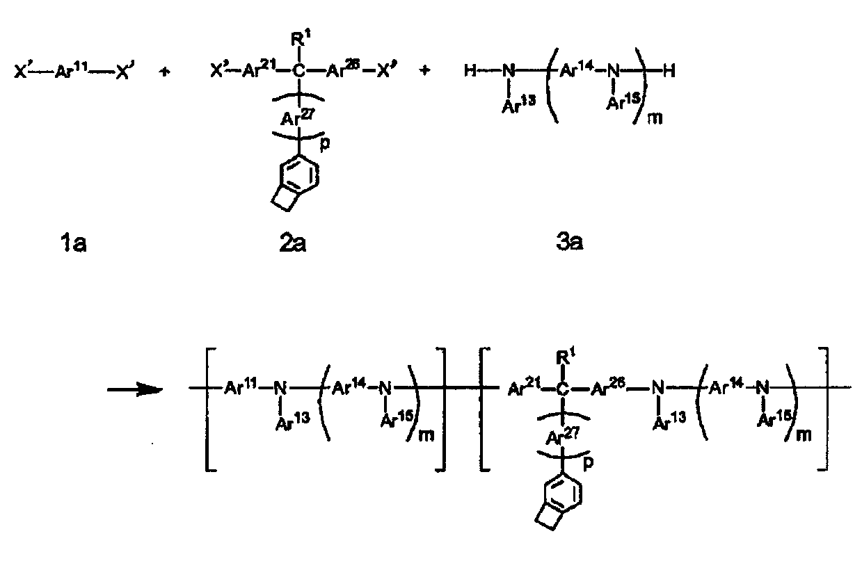
上記反応式中、X’はI、Br、Cl、F等のハロゲン原子を表す。
mは0~3の整数を表し、pは1~6の整数を表す。
Ar11は、直接結合、置換基を有していてもよい芳香族炭化水素基又は置換基を有していてもよい芳香族複素環基を表す。
Ar13~Ar15は、各々独立に、置換基を有していてもよい芳香族炭化水素基又は置換基を有していてもよい芳香族複素環基を表す。
Ar21は、直接結合、置換基を有していてもよい芳香族炭化水素基又は置換基を有していてもよい芳香族複素環基を表す。
Ar26及びAr27は、各々独立に、置換基を有していてもよい芳香族炭化水素基又は置換基を有していてもよい芳香族複素環基を表す。
R1は、水素原子、置換基を有していてもよい炭素数1~24のアルキル基、置換基を有していてもよい炭素数1~24のアルコキシ基、置換基を有してもよい芳香族炭化水素基又は置換基を有してもよい芳香族複素環基を表す。
p個のAr27は、同じでもよく、また異なっていてもよい。
m個のAr14同士及びAr15同士は、各々、同じでもよく、異なっていてもよい。
mは0~3の整数を表し、pは1~6の整数を表す。
Ar11は、直接結合、置換基を有していてもよい芳香族炭化水素基又は置換基を有していてもよい芳香族複素環基を表す。
Ar13~Ar15は、各々独立に、置換基を有していてもよい芳香族炭化水素基又は置換基を有していてもよい芳香族複素環基を表す。
Ar21は、直接結合、置換基を有していてもよい芳香族炭化水素基又は置換基を有していてもよい芳香族複素環基を表す。
Ar26及びAr27は、各々独立に、置換基を有していてもよい芳香族炭化水素基又は置換基を有していてもよい芳香族複素環基を表す。
R1は、水素原子、置換基を有していてもよい炭素数1~24のアルキル基、置換基を有していてもよい炭素数1~24のアルコキシ基、置換基を有してもよい芳香族炭化水素基又は置換基を有してもよい芳香族複素環基を表す。
p個のAr27は、同じでもよく、また異なっていてもよい。
m個のAr14同士及びAr15同士は、各々、同じでもよく、異なっていてもよい。
なお前記の重合方法において、通常、N-アリール結合を形成する反応は、例えば炭酸カリウム、tert-ブトキシナトリウム、トリエチルアミン等の塩基存在下で行う。例えば銅、ニッケル、パラジウム等の遷移金属触媒存在下で行うこともできる。
遷移金属触媒としては、パラジウム化合物とホスフィン配位子とを使用することが好ましい。
パラジウム化合物としては、塩化パラジウム、酢酸パラジウム、ビス(ジベンジリデンアセトン)パラジウム、トリス(ジベンジリデンアセトン)ジパラジウムクロロホルム錯体が好ましい。
ホスフィン配位子としては、トリ-tert-ブチルホスフィン、トリシクロヘキシルホスフィン、ジ-tert-ブチルフェニルホスフィン、ジ-tert-ブチル(4-ジメチルアミノフェニル)ホスフィン、2-ジシクロヘキシルホスフィノ-2',6’-ジメトキシビフェニルが好ましい。
遷移金属触媒としては、パラジウム化合物とホスフィン配位子とを使用することが好ましい。
パラジウム化合物としては、塩化パラジウム、酢酸パラジウム、ビス(ジベンジリデンアセトン)パラジウム、トリス(ジベンジリデンアセトン)ジパラジウムクロロホルム錯体が好ましい。
ホスフィン配位子としては、トリ-tert-ブチルホスフィン、トリシクロヘキシルホスフィン、ジ-tert-ブチルフェニルホスフィン、ジ-tert-ブチル(4-ジメチルアミノフェニル)ホスフィン、2-ジシクロヘキシルホスフィノ-2',6’-ジメトキシビフェニルが好ましい。
Suzuki反応のよる重合方法の場合、例えば、下記式1b及び2bで表されるホウ素誘導体と下記式3bで表されるジハロゲン化アリールを反応させることにより、本発明のポリマーが合成される。

上記反応式中、BR2はボロン酸基又はボロン酸エステル基を表す。
X’はI、Br、Cl、F等のハロゲン原子を表す。
mは0~3の整数を表し、pは1~6の整数を表す。
Ar12~Ar15は、各々独立に、置換基を有していてもよい芳香族炭化水素基又は置換基を有していてもよい芳香族複素環基を表す。
Ar21、Ar27、Ar31~Ar33は各々独立に、置換基を有していてもよい芳香族炭化水素基又は置換基を有していてもよい芳香族複素環基を表す。
R1は、水素原子、置換基を有していてもよいアルキル基、置換基を有していてもよいアルコキシ基、置換基を有してもよい芳香族炭化水素基又は置換基を有してもよい芳香族複素環基を表す。
p個のAr27は、同じでもよく、また異なっていてもよい。
m個のAr14同士及びAr15同士は、各々、同じでもよく、異なっていてもよい。
X’はI、Br、Cl、F等のハロゲン原子を表す。
mは0~3の整数を表し、pは1~6の整数を表す。
Ar12~Ar15は、各々独立に、置換基を有していてもよい芳香族炭化水素基又は置換基を有していてもよい芳香族複素環基を表す。
Ar21、Ar27、Ar31~Ar33は各々独立に、置換基を有していてもよい芳香族炭化水素基又は置換基を有していてもよい芳香族複素環基を表す。
R1は、水素原子、置換基を有していてもよいアルキル基、置換基を有していてもよいアルコキシ基、置換基を有してもよい芳香族炭化水素基又は置換基を有してもよい芳香族複素環基を表す。
p個のAr27は、同じでもよく、また異なっていてもよい。
m個のAr14同士及びAr15同士は、各々、同じでもよく、異なっていてもよい。
前記の重合方法において、通常、ホウ素誘導体とジハロゲン化物との反応工程は、例えば炭酸カリウム、tert-ブトキシナトリウム、トリエチルアミン等の塩基存在下で行う。必要に応じて、例えば銅やパラジウム錯体等の遷移金属触媒存在下で行うこともできる。ホウ素誘導体との反応工程は、例えば、炭酸カリウム、リン酸カリウム、tert-ブトキシナトリウム、トリエチルアミン等の塩基、及び、パラジウム錯体等の遷移金属触媒の存在下で行うことができる。
本発明の正孔輸送性ポリマーの製造には、上述した重合方法以外にも、特開2001-223084号公報に記載の重合方法、特開2003-213002号公報に記載の重合方法、特開2004-2740号公報に記載の重合方法、さらには、不飽和二重結合を有する化合物のラジカル重合、エステル結合やアミド結合を形成する反応による逐次重合などを用いることができる。
その他、公知のカップリング反応が使用可能である。公知のカップリング手法としては、具体的には、「Palladium in Heterocyclic Chemistry:A guide for the Synthetic Chemist」(第二版、2002、Jie Jack Li and Gordon W.Gribble、Pergamon社)、「遷移金属が拓く有機合成 その多彩な反応形式と最新の成果」(1997年、辻二郎、化学同仁社)、「ボルハルト・ショアー現代有機化学 下」(2004年、K.P.C.Vollhardt、化学同人社)などに記載又は引用されている、ハロゲン化アリールとアリールボレートとのカップリング反応などの、環同士の結合(カップリング)反応を用いることができる。
前記式(1A)~(1I)で表される基は、前述したように、予め本発明の正孔輸送性ポリマーの原料であるモノマーに結合させておき、これを重合することにより本発明の正孔輸送性ポリマーを得てもよいし、本発明の正孔輸送性ポリマーの主鎖にあたる部分を合成した後に、所望の部分に式(1A)~(1I)で表される基を結合してもよい。
化合物の精製方法としては、「分離精製技術ハンドブック」(1993年、(財)日本化学会編)、「化学変換法による微量成分及び難精製物質の高度分離」(1988年、(株)アイ ピー シー発行)、あるいは「実験化学講座(第4版)1」(1990年、(財)日本化学会編)の「分離と精製」の項に記載の方法をはじめとし、公知の技術を利用可能である。具体的には、抽出(懸濁洗浄、煮沸洗浄、超音波洗浄、酸塩基洗浄を含む)、吸着、吸蔵、融解、晶析(溶剤からの再結晶、再沈殿を含む)、蒸留(常圧蒸留、減圧蒸留)、蒸発、昇華(常圧昇華、減圧昇華)、イオン交換、透析、濾過、限外濾過、逆浸透、圧浸透、帯域溶解、電気泳動、遠心分離、浮上分離、沈降分離、磁気分離、各種クロマトグラフィー(形状分類:カラム、ペーパー、薄層、キャピラリー、移動相分類:ガス、液体、ミセル、超臨界流体。分離機構:吸着、分配、イオン交換、分子ふるい、キレート、ゲル濾過、排除、アフィニティー)などが挙げられる。
生成物の確認や純度の分析方法としては、ガスクロマトグラフ(GC)、高速液体クロマトグラフ(HPLC)、高速アミノ酸分析計(有機化合物)、キャピラリー電気泳動測定(CE)、サイズ排除クロマトグラフ(SEC)、ゲル浸透クロマトグラフ(GPC)、交差分別クロマトグラフ(CFC)、質量分析(MS、LC/MS,GC/MS,MS/MS)、核磁気共鳴装置(NMR(1HNMR,13CNMR))、フーリエ変換赤外分光高度計(FT-IR)、紫外可視近赤外分光高度計(UV.VIS,NIR)、電子スピン共鳴装置(ESR)、透過型電子顕微鏡(TEM-EDX)電子線マイクロアナライザー(EPMA)、金属元素分析(イオンクロマトグラフ、誘導結合プラズマ-発光分光(ICP-AES)原子吸光分析(AAS)、蛍光X線分析装置(XRF))、非金属元素分析、微量成分分析(ICP-MS,GF-AAS,GD-MS)等を、必要に応じ適用可能である。
<正孔輸送層>
本発明の有機フォトダイオードの正孔輸送層は、上述の本発明の正孔輸送性ポリマーを用いて好ましくは湿式成膜法により形成される。
本発明の有機フォトダイオードの正孔輸送層は、上述の本発明の正孔輸送性ポリマーを用いて好ましくは湿式成膜法により形成される。
湿式成膜法による正孔輸送層の形成には、本発明の正孔輸送性ポリマーと溶剤とを含む正孔輸送層形成用組成物(以下、「本発明の正孔輸送層形成用組成物」と称す場合がある。)が用いられる。
該溶剤は、本発明の正孔輸送性ポリマーを溶解するものが好ましく、通常、本発明の正孔輸送性ポリマーを常温で0.05重量%以上、好ましくは0.5重量%以上、さらに好ましくは1重量%以上溶解する溶剤である。
本発明の正孔輸送層形成用組成物に含有される溶剤としては、特に制限されるものではないが、本発明の正孔輸送性ポリマーを溶解させる必要があることから、例えば、エーテル系溶剤、エステル系溶剤、芳香族炭化水素系溶剤、アミド系溶剤などが好ましい。
エーテル系溶剤としては、例えば、エチレングリコールジメチルエーテル、エチレングリコールジエチルエーテル、プロピレングリコール-1-モノメチルエーテルアセタート(PGMEA)等の脂肪族エーテル及び1,2-ジメトキシベンゼン、1,3-ジメトキシベンゼン、アニソール、フェネトール、2-メトキシトルエン、3-メトキシトルエン、4-メトキシトルエン、2,3-ジメチルアニソール、2,4-ジメチルアニソール等の芳香族エーテル等が挙げられる。
エステル系溶剤としては、例えば、酢酸フェニル、プロピオン酸フェニル、安息香酸メチル、安息香酸エチル、安息香酸プロピル、安息香酸n-ブチル等の芳香族エステル等が挙げられる。
芳香族炭化水素系溶剤としては、例えば、トルエン、キシレン、シクロヘキシルベンゼン、3-イソプロピルビフェニル、1,2,3,4-テトラメチルベンゼン、1,4-ジイソプロピルベンゼン、シクロヘキシルベンゼン、メチルナフタレン等が挙げられる。
アミド系溶剤としては、例えば、N,N-ジメチルホルムアミド、N,N-ジメチルアセトアミド等が挙げられる。
これらの他、ジメチルスルホキシド等も用いることができる。
本発明の正孔輸送層形成用組成物における本発明の正孔輸送性ポリマーの濃度は、本発明の効果を著しく損なわない限り任意であるが、膜厚の均一性の点では低い方が好ましく、一方、正孔輸送層に欠陥が生じ難い点では高い方が好ましい。具体的には、0.01重量%以上が好ましく、0.1重量%以上が更に好ましく、0.5重量%以上が特に好ましい。また、70重量%以下が好ましく、60重量%以下が更に好ましく、50重量%以下が特に好ましい。
本発明の正孔輸送層形成用組成物中の溶剤の濃度は、通常10重量%以上、好ましくは30重量%以上、より好ましくは50重量%以上である。
本発明の正孔輸送層形成用組成物を用いて正孔輸送層を成膜する場合、正孔輸送層形成用組成物の塗布後、通常加熱を行う。本発明の正孔輸送層形成用組成物を用いて形成された層の加熱の手法は特に限定されない。加熱乾燥の場合の加熱温度の条件は、通常100℃以上、好ましくは120℃以上、より好ましくは150℃以上、通常400℃以下、好ましくは350℃以下、より好ましくは300℃以下である。加熱時間は、通常1分以上、好ましくは24時間以下である。加熱手段としては特に限定されないが、形成された層を有する積層体をホットプレート上に載せたり、オーブン内で加熱するなどの手段が用いられる。例えば、ホットプレート上で120℃以上、1分間以上加熱する等の条件を用いることができる。
正孔輸送層の膜厚は、通常5nm以上、好ましくは10nm以上であり、通常300nm以下、好ましくは100nm以下である。
正孔輸送層の膜厚が上記下限以上であれば、ブロッキング層として正孔輸送層を設けたことによる暗電流の低減効果を有効に得ることができる。正孔輸送層の膜厚が上記上限以下であれば、本発明の有機フォトダイオードを利用したCMOSセンサーにおいて光の入射角を広くとることが可能であり、また、有機フォトダイオードの薄膜化を図ることができる。
暗電流を効果的に低減するために、正孔輸送層は光電変換層のn型半導体に対して0.3eV以上浅いLUMOを有していることが好ましく、0.5eV以上浅いLUMOを有していることが好ましく、1.0eV以上浅いLUMOを有することがさらに好ましい。
正孔輸送層は光電変換層で発生した正孔を効率よく第1電極へと運ぶ役割を果たすことから、光電変換層のp型半導体とのHOMOの差が0.5eV以内であることが好ましく、0.3eV以内であることが好ましい。
正孔輸送層は光電変換層で発生した正孔を効率よく第1電極へと運ぶ役割を果たすことから、光電変換層のp型半導体とのHOMOの差が0.5eV以内であることが好ましく、0.3eV以内であることが好ましい。
<基板>
本発明の有機フォトダイオードは、第1電極、正孔輸送層、光電変換層、及び第2電極がこの順で積層形成されたものであるが、通常、これらの層を支持するために、基板を備えている。基板は、第1電極側、第2電極側のいずれに設けられていてもよく、両側に設けられてもよい。基板は少なくとも、第1電極側に設けられていることが好ましい。
本発明の有機フォトダイオードは、第1電極、正孔輸送層、光電変換層、及び第2電極がこの順で積層形成されたものであるが、通常、これらの層を支持するために、基板を備えている。基板は、第1電極側、第2電極側のいずれに設けられていてもよく、両側に設けられてもよい。基板は少なくとも、第1電極側に設けられていることが好ましい。
基板は、任意の材料により形成することが可能である。光を基板側から入射する場合は、透明性の高い材料で形成する必要がある。
基板の構成材料の例を挙げると、ガラス、サファイア、チタニア等の無機材料;ポリエチレンテレフタレート、ポリエチレンナフタレート、ポリエーテルスルホン、ポリイミド、ナイロン、ポリスチレン、ポリビニルアルコール、エチレンビニルアルコール共重合体、フッ素樹脂、塩化ビニル、ポリエチレン、セルロース、ポリ塩化ビニリデン、アラミド、ポリフェニレンスルフィド、ポリウレタン、ポリカーボネート、ポリアリレート、ポリノルボルネン等の有機材料;紙、合成紙等の紙材料;ステンレス、チタン、アルミニウム等の金属に、絶縁性を付与するために表面をコート或いはラミネートしたもの等の複合材料などが挙げられる。基板の構成材料は、1種を単独で用いてもよく、2種以上を任意の組み合わせ及び比率で併用しても良い。
基板の形状及び寸法に制限はなく、任意に設定することができる。
基板には、ガスバリヤー性の付与や表面状態の制御のために、別の層を積層してもよい。
基板の厚さは、有機フォトダイオードの用途、構成材料等に応じて任意に設計可能である。基板の厚さは、過度に薄いと、強度が不足して支持部材としての機能を果たし得ず、過度に厚いとコストアップとなる。基板は、通常10μm~50mm程度のフィルム状ないし板状とされる。
<電極>
電極(第1電極、第2電極)は、導電性を有する任意の材料により形成することが可能である。
電極(第1電極、第2電極)は、導電性を有する任意の材料により形成することが可能である。
電極の構成材料の例を挙げると、白金、金、銀、アルミニウム、クロム、ニッケル、銅、チタン、マグネシウム、カルシウム、バリウム、ナトリウム等の金属あるいはそれらの合金;酸化インジウムや酸化錫等の金属酸化物、あるいはその複合酸化物(例えばITO、IZO);ポリアニリン、ポリピロール、ポリチオフェン、ポリアセチレン等の導電性高分子;前記導電性高分子に、塩酸、硫酸、スルホン酸等の酸、FeCl3等のルイス酸、ヨウ素等のハロゲン原子、ナトリウム、カリウム等の金属原子などのドーパントを添加したもの;金属粒子、カーボンブラック、フラーレン、カーボンナノチューブ等の導電性粒子をポリマーバインダー等のマトリクスに分散した導電性の複合材料などが挙げられる。電極の構成材料は、1種を単独で用いてもよく、2種以上を任意の組み合わせ及び比率で併用しても良い。
有機フォトダイオードにおいて、電極は少なくとも一対(2個)設けられ、この一対の電極の間に光電変換層が設けられる。この際、一対の電極のうち、少なくとも一方は透明である(即ち、発電のために光電変換層が吸収する光を透過させる)ことが好ましい。
透明な電極の材料を挙げると、例えば、酸化インジウムスズ(ITO)、酸化インジウム亜鉛(IZO)等の複合酸化物;金属薄膜などが挙げられる。
この際の光の透過率の具体的範囲に制限は無いが、有機フォトダイオードの光電変換効率を考慮すると、80%以上が好ましい。光の透過率は、通常の分光光度計で測定可能できる。
この際の光の透過率の具体的範囲に制限は無いが、有機フォトダイオードの光電変換効率を考慮すると、80%以上が好ましい。光の透過率は、通常の分光光度計で測定可能できる。
電極は、光電変換層内に生じた正孔及び電子を捕集する機能を有するものである。従って、電極の構成材料としては、上述した材料のうち、正孔及び電子を捕集するのに適した構成材料を用いることが好ましい。正孔の捕集に適した電極の材料を挙げると、例えば、Au、ITO等の高い仕事関数を有する材料が挙げられる。電子の捕集に適した電極の材料を挙げると、例えば、Alのような低い仕事関数を有する材料が挙げられる。
電極の厚さには特に制限はなく、用いた材料と、必要とされる導電性、透明性等を考慮して適宜決定される。電極の厚さは通常10nm~100μm程度である。
電極の形成方法に制限はない。電極は例えば、真空蒸着、スパッタ等のドライプロセスにより形成することができる。また、例えば、導電性インク等を用いたウェットプロセスにより形成することもできる。この際、導電性インクとしては任意のものを使用することができ、例えば、導電性高分子、金属粒子分散液等を用いることができる。電極は2層以上積層してもよく、特性(電気特性やぬれ特性等)改良のための表面処理を施してもよい。
<光電変換層>
光電変換層は、光を吸収して電荷を分離する層である。本発明の有機フォトダイオードの光電変換層は、p型半導体とn型半導体を含む。光電変換層がp型半導体とn型半導体とを含む混合半導体膜よりなるバルクヘテロ接合構造であることにより、p型半導体とn型半導体との距離が近づくことで、光電変換効率の高い有機フォトダイオードを実現することができる。
光電変換層は、光を吸収して電荷を分離する層である。本発明の有機フォトダイオードの光電変換層は、p型半導体とn型半導体を含む。光電変換層がp型半導体とn型半導体とを含む混合半導体膜よりなるバルクヘテロ接合構造であることにより、p型半導体とn型半導体との距離が近づくことで、光電変換効率の高い有機フォトダイオードを実現することができる。
本発明に係る光電変換層に含まれるp型半導体及びn型半導体としては、それぞれキナクリドン誘導体、ナフタレン誘導体、アントラセン誘導体、フェナントレン誘導体、テトラセン誘導体、ピレン誘導体、ペリレン誘導体、及びフルオランテン誘導体のいずれかを特に好ましく用いることができる。
p型半導体(化合物)は、ドナー性半導体(化合物)であり、主に正孔輸送性化合物に代表され、電子を供与しやすい性質がある化合物をいう。さらに詳しくは2つの材料を接触させて用いたときにイオン化ポテンシャルの小さい方の化合物をいう。したがって、ドナー性化合物は、電子供与性のある化合物であればいずれの化合物も使用可能である。例えば、トリアリールアミン化合物、ベンジジン化合物、ピラゾリン化合物、スチリルアミン化合物、ヒドラゾン化合物、トリフェニルメタン化合物、カルバゾール化合物、ポリシラン化合物、チオフェン化合物、フタロシアニン化合物、シアニン化合物、メロシアニン化合物、オキソノール化合物、ポリアミン化合物、インドール化合物、ピロール化合物、ピラゾール化合物、ポリアリーレン化合物、縮合芳香族炭素環化合物(ナフタレン誘導体、アントラセン誘導体、フェナントレン誘導体、テトラセン誘導体、ピレン誘導体、ペリレン誘導体、フルオランテン誘導体)、含窒素ヘテロ環化合物を配位子として有する金属錯体等を用いることができる。
これに限らず、上記したように、n型(アクセプター性)化合物として用いた化合物よりもイオン化ポテンシャルの小さい化合物であればドナー性半導体として用いてよい。
これに限らず、上記したように、n型(アクセプター性)化合物として用いた化合物よりもイオン化ポテンシャルの小さい化合物であればドナー性半導体として用いてよい。
n型半導体(化合物)は、アクセプター性半導体(化合物)であり、主に電子輸送性化合物に代表され、電子を受容しやすい性質がある化合物をいう。さらに詳しくは2つの化合物を接触させて用いたときに電子親和力の大きい方の化合物をいう。したがって、アクセプター性化合物は、電子受容性のある化合物であればいずれの化合物も使用可能である。
例えば、縮合芳香族炭素環化合物(ナフタレン誘導体、アントラセン誘導体、フェナントレン誘導体、テトラセン誘導体、ピレン誘導体、ペリレン誘導体、フルオランテン誘導体)、窒素原子、酸素原子、硫黄原子を含有する5ないし7員のヘテロ環化合物(例えばピリジン、ピラジン、ピリミジン、ピリダジン、トリアジン、キノリン、キノキサリン、キナゾリン、フタラジン、シンノリン、イソキノリン、プテリジン、アクリジン、フェナジン、フェナントロリン、テトラゾール、ピラゾール、イミダゾール、チアゾール、オキサゾール、インダゾール、ベンズイミダゾール、ベンゾトリアゾール、ベンゾオキサゾール、ベンゾチアゾール、カルバゾール、プリン、トリアゾロピリダジン、トリアゾロピリミジン、テトラザインデン、オキサジアゾール、イミダゾピリジン、ピラリジン、ピロロピリジン、チアジアゾロピリジン、ジベンズアゼピン、トリベンズアゼピン等)、ポリアリーレン化合物、フルオレン化合物、シクロペンタジエン化合物、シリル化合物、含窒素ヘテロ環化合物を配位子として有する金属錯体などが挙げられる。
これに限らず、上記したように、ドナー性化合物として用いた化合物よりも電子親和力の大きな化合物であればアクセプター性半導体として用いてよい。
例えば、縮合芳香族炭素環化合物(ナフタレン誘導体、アントラセン誘導体、フェナントレン誘導体、テトラセン誘導体、ピレン誘導体、ペリレン誘導体、フルオランテン誘導体)、窒素原子、酸素原子、硫黄原子を含有する5ないし7員のヘテロ環化合物(例えばピリジン、ピラジン、ピリミジン、ピリダジン、トリアジン、キノリン、キノキサリン、キナゾリン、フタラジン、シンノリン、イソキノリン、プテリジン、アクリジン、フェナジン、フェナントロリン、テトラゾール、ピラゾール、イミダゾール、チアゾール、オキサゾール、インダゾール、ベンズイミダゾール、ベンゾトリアゾール、ベンゾオキサゾール、ベンゾチアゾール、カルバゾール、プリン、トリアゾロピリダジン、トリアゾロピリミジン、テトラザインデン、オキサジアゾール、イミダゾピリジン、ピラリジン、ピロロピリジン、チアジアゾロピリジン、ジベンズアゼピン、トリベンズアゼピン等)、ポリアリーレン化合物、フルオレン化合物、シクロペンタジエン化合物、シリル化合物、含窒素ヘテロ環化合物を配位子として有する金属錯体などが挙げられる。
これに限らず、上記したように、ドナー性化合物として用いた化合物よりも電子親和力の大きな化合物であればアクセプター性半導体として用いてよい。
n型半導体としてフラーレン骨格を有するものを用いると、光電変換効率を高めるために、バルクヘテロ接合構造としても、嵩高いフラーレン骨格の存在でn型半導体とp型半導体との距離が離れてしまい、光電変換効率が低下してしまう。
従って、本発明におけるn型半導体は、フラーレン骨格を有するn型半導体の割合がフラーレン骨格を有さないn型半導体に対して10重量%以下であることが好ましく、n型半導体中にフラーレン骨格を有するものが実質的に含まれていないことがより好ましい。
ここで、「フラーレン骨格を実質的に含まない」とは、光電変換層において発生した電荷の内、電子の輸送を非フラーレン型のn型半導体が担うという意味であり、光電変換層のモルフォロジーの改善のために少量含有することはあり得る。そのような目的においては、通常フラーレン骨格を含むn型半導体は、フラーレン骨格を有さない非フラーレン型のn型半導体に対して5重量%以下で含有されており、好ましくはこの割合は2重量%以下である。
ここで、「フラーレン骨格を実質的に含まない」とは、光電変換層において発生した電荷の内、電子の輸送を非フラーレン型のn型半導体が担うという意味であり、光電変換層のモルフォロジーの改善のために少量含有することはあり得る。そのような目的においては、通常フラーレン骨格を含むn型半導体は、フラーレン骨格を有さない非フラーレン型のn型半導体に対して5重量%以下で含有されており、好ましくはこの割合は2重量%以下である。
前掲の特許文献3には、バルクヘテロ接合構造におけるp型半導体とn型半導体の接触に起因する暗電流発生の問題を、n型半導体にフラーレン骨格を導入することで抑制することが記載されている。しかし、n型半導体にフラーレン骨格を導入すると、バルクヘテロ接合構造の効果が低減され、光電変換効率が落ちてしまう。
本発明では、バルクヘテロ接合構造としたことによる暗電流発生の問題を正孔輸送層に本発明の正孔輸送性ポリマーを用いることで抑制することができるため、n型半導体としてフラーレン骨格のないものを用い、バルクヘテロ接合構造による光電変換効率の向上効果を有効に発揮させる。
光電変換層に含まれるp型半導体とn型半導体の割合は、p型半導体に対するn型半導体の重量比率(n型半導体/p型半導体重量比)で0.5~2.5倍、特に1.0~2.0倍であることが好ましい。上記範囲よりもn型半導体が多くp型半導体が少ないと、近赤外領域における感度が低下する傾向がある。上記範囲よりも逆にp型半導体が多くn型半導体が少ないと、暗電流が発生し易い傾向にある。
本発明において、光電変換層のn型半導体としては、公知の種々のn型半導体を使用することができるが、好ましくは下記式(4)で表されるn型半導体が挙げられる。

式(4)中、Dは多環芳香族を有するドナー部位を表す。Aはマロノニトリル基を有するアクセプター部位を表す。
このうち、より好ましい構造としては、下記式(5)で表されるn型半導体が挙げられる。

式(5)中、Ar41はそれぞれ独立に下記式(5a-1)~(5g-1)で表される。
Ar42はそれぞれ独立に下記式(5a-2)~(5d-2)で表される。
Ar43はそれぞれ独立に下記式(5a-3)~(5d-3)で表される。
Ar42はそれぞれ独立に下記式(5a-2)~(5d-2)で表される。
Ar43はそれぞれ独立に下記式(5a-3)~(5d-3)で表される。

上記式(5a-1)~(5g-1),(5a-2)~(5d-2),(5a-3)~(5d-3)中、*は結合部位を表す。
XはC=O、O、S、又はSeを表す。
YはCR31R31、SiR31R31、GeR31R31、NR31、又はC=Oを表す。
ZはCR31、又はNを表す。
LはR31、又はハロゲン原子を表す。
R31はそれぞれ独立に、水素原子、分岐を有していてもよい炭素数1~30のアルキル基、分岐を有していてもよい炭素数1~30のアルコキシ基、或いは分岐を有していてもよい炭素数1~30のアルキル基及び/又は分岐を有していてもよい炭素数1~30のアルコキシ基で置換されていてもよいフェニル基を表す。
Aはマロノニトリル基を有するアクセプター部位を表す。
x1は0又は1、x2は1~6の整数、x3は0又は1をそれぞれ表す。
式(5)において、式(5f-1)と式(5g-1)とが隣接することはない。
XはC=O、O、S、又はSeを表す。
YはCR31R31、SiR31R31、GeR31R31、NR31、又はC=Oを表す。
ZはCR31、又はNを表す。
LはR31、又はハロゲン原子を表す。
R31はそれぞれ独立に、水素原子、分岐を有していてもよい炭素数1~30のアルキル基、分岐を有していてもよい炭素数1~30のアルコキシ基、或いは分岐を有していてもよい炭素数1~30のアルキル基及び/又は分岐を有していてもよい炭素数1~30のアルコキシ基で置換されていてもよいフェニル基を表す。
Aはマロノニトリル基を有するアクセプター部位を表す。
x1は0又は1、x2は1~6の整数、x3は0又は1をそれぞれ表す。
式(5)において、式(5f-1)と式(5g-1)とが隣接することはない。
さらに好ましいn型半導体としては、前記Aのマロノニトリル基を有するアクセプター部位が、下記式(5A)~(5C)のいずれかで表されるものが挙げられる。

上記式(5A)~(5C)中、*は結合部位を表す。
Qはマロノニトリル基もしくはO=を表す。Qの少なくとも一方はマロノニトリル基である。
XはC=O、O、S、又はSeを表す。
RAはそれぞれ独立に、水素原子、ハロゲン原子、分岐を有していてもよい炭素数1~30のアルキル基、分岐を有していてもよい炭素数1~30のアルコキシ基、或いは分岐を有していてもよい炭素数1~30のアルキル基及び/又は分岐を有していてもよい炭素数1~30のアルコキシ基で置換されていてもよいフェニル基を表す。
RBはRAと同義であるか、或いは隣接するRB同士で芳香族6員環を形成する。
Qはマロノニトリル基もしくはO=を表す。Qの少なくとも一方はマロノニトリル基である。
XはC=O、O、S、又はSeを表す。
RAはそれぞれ独立に、水素原子、ハロゲン原子、分岐を有していてもよい炭素数1~30のアルキル基、分岐を有していてもよい炭素数1~30のアルコキシ基、或いは分岐を有していてもよい炭素数1~30のアルキル基及び/又は分岐を有していてもよい炭素数1~30のアルコキシ基で置換されていてもよいフェニル基を表す。
RBはRAと同義であるか、或いは隣接するRB同士で芳香族6員環を形成する。
n型半導体が(4)式のような構造を有することにより、分子内相互作用が発生して電子移動度や光電変換効率の点で好ましい。
式(5)におけるAr41、Ar42が上記(5a-1)~(5g-1)、(5a-2)~(5d-2)で表される構造を取ると、ドナー部位の平面性・電子供与性が向上してn型半導体の分子内相互作用が強くなり、電子移動度や光電変換効率の点で好ましく、光の吸収波長を長波長化させる点で好ましい。
n型半導体においてAr43が(5a-3)~(5d-3)のような構造を有すると、ドナー部位の電子供与性がさらに高まり、光の吸収波長をさらに長波長化させる点で好ましい。
式(5)においてアクセプター部位Aが(5A)~(5C)のような構造を有すると、アクセプター部位の平面性・電子吸引性を向上させることができ、n型半導体の分子間相互作用が強くなるので、電子移動度や光電変換効率の点で好ましい。
このようなバルクヘテロ接合構造の光電変換層の形成方法には特に制限はないが、例えば、p型半導体とn型半導体の所定量を適用な溶剤に溶解させて調製した光電変換層形成用組成物を用いる湿式成膜法により形成することができる。
この光電変換層形成用組成物に用いる溶剤としては、p型半導体及びn型半導体を溶解し得るものであればよく、例えば、トルエン、キシレン、メシチレン、シクロヘキシルベンゼン等の芳香族系溶媒;1,2-ジクロロエタン、クロロベンゼン、o-ジクロロベンゼン等の含ハロゲン溶媒;エチレングリコールジメチルエーテル、エチレングリコールジエチルエーテル、プロピレングリコール-1-モノメチルエーテルアセタート(PGMEA)等の脂肪族エーテル、1,2-ジメトキシベンゼン、1,3-ジメトキシベンゼン、アニソール、フェネトール、2-メトキシトルエン、3-メトキシトルエン、4-メトキシトルエン、2,3-ジメチルアニソール、2,4-ジメチルアニソール等の芳香族エーテル等のエーテル系溶媒;酢酸エチル、酢酸n-ブチル、乳酸エチル、乳酸n-ブチル等の脂肪族エステル系溶媒;酢酸フェニル、プロピオン酸フェニル、安息香酸メチル、安息香酸エチル、安息香酸イソプロピル、安息香酸プロピル、安息香酸n-ブチル等の芳香族エステル等のエステル系溶媒;などが挙げられる。
本発明に係る光電変換層の膜厚は、光電変換層の構成や有機フォトダイオードの用途に応じて任意に設計することができる。光電変換層の膜厚が、過ぎると光吸収が不十分で効率が低下し、厚過ぎると内部抵抗が増大して損失が大きくなる。光電変換層の膜厚は通常10nm~1μm程度とされる。
<電子輸送層>
電子輸送層は、本発明の有機フォトダイオードに必ずしも必要とされるものではないが、光電変換層と第2電極との間に電子輸送層を設けることで、光電変換効率を高めたり、暗電流を低減したりすることができる。
電子輸送層は、本発明の有機フォトダイオードに必ずしも必要とされるものではないが、光電変換層と第2電極との間に電子輸送層を設けることで、光電変換効率を高めたり、暗電流を低減したりすることができる。
電子輸送層は、光電変換層で生成した電子を効率よく第2電極に輸送することができる化合物より形成される。電子輸送層に用いられる電子輸送性化合物としては、光電変換層からの電子注入効率が高く、かつ、高い電子移動度を有し注入された電子を効率よく輸送することができる化合物であることが必要である。
このために、電子輸送層は光電変換層のn型半導体とのLUMOの差が1.5eV以下であることが好ましく、1.0eVであることが好ましい。
電子輸送層によって暗電流を低減させる場合、電子輸送層は光電変換層のp型半導体に対して0.3eV以上深いHOMOを有していることが好ましく、0.5eV以上深いHOMOを有していることが好ましく、1.0eV以上深いHOMOを有していることがさらに好ましい。
電子輸送層によって暗電流を低減させる場合、電子輸送層は光電変換層のp型半導体に対して0.3eV以上深いHOMOを有していることが好ましく、0.5eV以上深いHOMOを有していることが好ましく、1.0eV以上深いHOMOを有していることがさらに好ましい。
電子輸送層に用いる電子輸送性化合物としては、例えば、8-ヒドロキシキノリンのアルミニウム錯体などの金属錯体(特開昭59-194393号公報)、10-ヒドロキシベンゾ[h]キノリンの金属錯体、オキサジアゾール誘導体、ジスチリルビフェニル誘導体、シロール誘導体、3-ヒドロキシフラボン金属錯体、5-ヒドロキシフラボン金属錯体、ベンズオキサゾール金属錯体、ベンゾチアゾール金属錯体、トリスベンズイミダゾリルベンゼン(米国特許第5645948号明細書)、キノキサリン化合物(特開平6-207169号公報)、フェナントロリン誘導体(特開平5-331459号公報)、2-t-ブチル-9,10-N,N’-ジシアノアントラキノンジイミン、n型水素化非晶質炭化シリコン、n型硫化亜鉛、n型セレン化亜鉛などが挙げられる。
電子輸送層の形成材料として、酸化チタン、酸化亜鉛、酸化スズ、酸化セリウムなどの金属酸化物を用いることもできる。その場合、電子輸送層の成膜方法としては、金属酸化物のナノ粒子を湿式成膜して乾燥して金属酸化物層とする方法や、前駆体を湿式成膜して加熱変換する方法を用いることができる。
電子輸送層の膜厚は、通常1nm以上、好ましくは5nm以上であり、通常300nm以下、好ましくは100nm以下である。
電子輸送層は、湿式成膜法或いは真空蒸着法により形成することができるが、通常、真空蒸着法が用いられる。
<その他の構成層>
本発明の有機フォトダイオードは、本発明の効果を著しく損なわなければ、上述した基板、第1及び第2電極、正孔輸送層、光電変換層及び電子輸送層以外の構成層を備えていても良い。
本発明の有機フォトダイオードは、本発明の効果を著しく損なわなければ、上述した基板、第1及び第2電極、正孔輸送層、光電変換層及び電子輸送層以外の構成層を備えていても良い。
例えば、有機フォトダイオードは、外気の影響を最小限にするために、光電変換層部分、更には電極部分を含めて覆うように保護膜を備えていても良い。保護層は、例えば、スチレン樹脂、エポキシ樹脂、アクリル樹脂、ポリウレタン、ポリイミド、ポリビニルアルコール、ポリフッ化ビニリデン、ポリエチレンポリビニルアルコール共重合体等のポリマー膜;酸化珪素、窒化珪素、酸化アルミニウム等の無機酸化膜や窒化膜;あるいはこれらの積層膜などにより構成することができる。
前記の保護膜の形成方法に制限はない。
例えば、保護膜をポリマー膜とする場合には、ポリマー溶液の塗布乾燥による形成方法、モノマーを塗布或いは蒸着して重合する形成方法などが挙げられる。
ポリマー膜の形成に際しては、さらに架橋処理を行なったり、多層膜を形成したりすることも可能である。
保護膜を無機酸化膜や窒化膜等の無機物膜とする場合には、例えば、スパッタ法、蒸着法等の真空プロセスでの形成方法、ゾルゲル法に代表される溶液プロセスでの形成方法などを用いることができる。
例えば、保護膜をポリマー膜とする場合には、ポリマー溶液の塗布乾燥による形成方法、モノマーを塗布或いは蒸着して重合する形成方法などが挙げられる。
ポリマー膜の形成に際しては、さらに架橋処理を行なったり、多層膜を形成したりすることも可能である。
保護膜を無機酸化膜や窒化膜等の無機物膜とする場合には、例えば、スパッタ法、蒸着法等の真空プロセスでの形成方法、ゾルゲル法に代表される溶液プロセスでの形成方法などを用いることができる。
光電変換層で発生した電荷を効率よく電極に捕集させるために、第1電極と正孔輸送層との間、あるいは電子輸送層と第2電極との間に電荷注入層を備えていてもよい。
有機フォトダイオードは、例えば紫外線を透過させない光学フィルタを光の入射側に備えていてもよい。紫外線は一般に有機フォトダイオードの劣化を促進することが多いため、紫外線を遮断することにより、有機フォトダイオードを長寿命化させることができる。
<有機フォトダイオードの製造方法>
本発明の有機フォトダイオードは、通常、基板上に、第1電極、正孔輸送層、光電変換層、第2電極の順でこれらの層をそれぞれ前述した方法で積層形成することにより製造される。これらの層間に必要に応じて設けられる電子輸送層等の形成工程が設けられる。
本発明の有機フォトダイオードは、通常、基板上に、第1電極、正孔輸送層、光電変換層、第2電極の順でこれらの層をそれぞれ前述した方法で積層形成することにより製造される。これらの層間に必要に応じて設けられる電子輸送層等の形成工程が設けられる。
〔赤外線CMOSセンサー〕
本発明の赤外線CMOSセンサーは、本発明の有機フォトダイオードを用いた赤外線CMOSセンサーである。本発明の赤外線CMOSセンサーは、有機フォトダイオードとして本発明の有機フォトダイオードを用いること以外は、従来の一般的な赤外線CMOSセンサーの構成を採用することができる。本発明の赤外線CMOSセンサーは、例えば、図2に示すような構成とすることができる。
本発明の赤外線CMOSセンサーは、本発明の有機フォトダイオードを用いた赤外線CMOSセンサーである。本発明の赤外線CMOSセンサーは、有機フォトダイオードとして本発明の有機フォトダイオードを用いること以外は、従来の一般的な赤外線CMOSセンサーの構成を採用することができる。本発明の赤外線CMOSセンサーは、例えば、図2に示すような構成とすることができる。
図2の赤外線CMOSセンサーは、保護膜3を有する本発明の有機フォトダイオード10が、トランジスタ6及び信号蓄積部7を有するシリコン基板5上の金属配線層4上に設けられており、この有機フォトダイオード10上にカラーフィルタ2を介してマイクロレンズ1が載置されている。カラーフィルター2は図2では便宜上R,G,Bとしているが、可視光カットフィルターを載置して近赤外線のみに感度を有するようにすることもできる。
有機フォトダイオード10の下部電極11は、カラーフィルタ2のカラーR,G,Bに対応して分割されている。有機フォトダイオード10の有機光電膜20は、図1に示す通り、下部電極11側から、正孔輸送層12、光電変換層13、電子輸送層14が積層されている。
カラーフィルタ2のR,G,Bの各色に対応する下部電極11と、それに対向する上部電極15と、これらに挟まれる光電変換層の一部とにより、カラーフィルタ2に対応する光電変換素子が形成されている。
赤外線CMOSセンサーに入射した光は画素ごとに設けられたマイクロレンズ1、カラーフィルタ2を介して有機フォトダイオード10に吸収され、電子正孔対が生成される。発生した電子は、光電変換層13に印加される電界強度に応じて下部電極11側に引き抜かれ、信号荷電として信号蓄積部7に蓄積される。
赤外線CMOSセンサーに入射した光は画素ごとに設けられたマイクロレンズ1、カラーフィルタ2を介して有機フォトダイオード10に吸収され、電子正孔対が生成される。発生した電子は、光電変換層13に印加される電界強度に応じて下部電極11側に引き抜かれ、信号荷電として信号蓄積部7に蓄積される。
以下、実施例により本発明を更に詳細に説明するが、本発明はその要旨を超えない限り以下の実施例に限定されるものではない。
[評価方法]
以下の実施例及び比較例で製造した有機フォトダイオードの性能測定方法は以下の通りである。
以下の実施例及び比較例で製造した有機フォトダイオードの性能測定方法は以下の通りである。
擬似太陽光装置・電気特性測定機器(分光計器社製)による分光感度の測定から、波長940nmにおいて、素子に-1Vの電圧を印加した際の外部量子効率の値を得た。
また、同装置内に暗箱を設け、2400ソースメーターを用いて、素子に-1Vの電圧を印加した際の電流電圧測定により単位面積当たりの暗電流密度の値を得た。
また、素子の受光部分に1mm□の開口を有する遮光マスクを設置し、ペクセル・テクノロジー社製の作用スペクトル測定装置PEC-S20を用いて波長850nmの光に対する光電変換効率を測定した。
測定に当たっては、ITO基板側から光を入射させた。
また、同装置内に暗箱を設け、2400ソースメーターを用いて、素子に-1Vの電圧を印加した際の電流電圧測定により単位面積当たりの暗電流密度の値を得た。
また、素子の受光部分に1mm□の開口を有する遮光マスクを設置し、ペクセル・テクノロジー社製の作用スペクトル測定装置PEC-S20を用いて波長850nmの光に対する光電変換効率を測定した。
測定に当たっては、ITO基板側から光を入射させた。
<実施例1>
以下の方法により、有機フォトダイオードを作製した。
ガラス基板上に電極として膜厚150nmのインジウム・スズ酸化物(ITO)の透明導電膜がパターン成膜されたITO基板の表面を紫外線オゾン洗浄機(NL-UV253、日本レーザー電子社製)で10分間処理した後に、正孔輸送層を次のように成膜した。
以下の方法により、有機フォトダイオードを作製した。
ガラス基板上に電極として膜厚150nmのインジウム・スズ酸化物(ITO)の透明導電膜がパターン成膜されたITO基板の表面を紫外線オゾン洗浄機(NL-UV253、日本レーザー電子社製)で10分間処理した後に、正孔輸送層を次のように成膜した。
下記式(H4)に示すポリマー(Mw=64000、Mn=43000、Mw/Mn=1.5)16mgを1mLのトルエンに溶解させ、正孔輸送層形成用組成物を調製した。
なお、下記式(H4)において、0.95の比率で含まれる繰り返し単位中のArは、下に0.95と記載されている9,9-ジn-ヘキシル-2-フルオレニル基であり、ランダムに0.95:0.05の割合で含まれているわけではない。0.05の繰り返し単位についても同様である。
この組成物を窒素雰囲気下において回転数1500rpmで30秒間、ITO基板の電極面にスピンコートし、240℃で30分間加熱乾燥して、膜厚92nmの正孔輸送層を形成した。なお、下記式(H4)に示すポリマーは、230℃の加熱乾燥でも重合し、その後の塗布工程を行っても問題を生じるものではない。
なお、下記式(H4)において、0.95の比率で含まれる繰り返し単位中のArは、下に0.95と記載されている9,9-ジn-ヘキシル-2-フルオレニル基であり、ランダムに0.95:0.05の割合で含まれているわけではない。0.05の繰り返し単位についても同様である。
この組成物を窒素雰囲気下において回転数1500rpmで30秒間、ITO基板の電極面にスピンコートし、240℃で30分間加熱乾燥して、膜厚92nmの正孔輸送層を形成した。なお、下記式(H4)に示すポリマーは、230℃の加熱乾燥でも重合し、その後の塗布工程を行っても問題を生じるものではない。
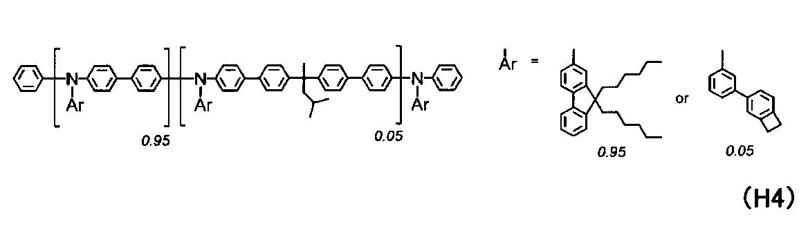
この正孔輸送層上に次のようにして光電変換層を成膜した。
光電変換層は、p型半導体PCE-10(アルドリッチ社製)と、n型半導体材料として下記式(N2)で表されるもの(式(N2)において、Rはすべて2-エチルヘキシル基)を、1対1の重量比で秤量し、クロロベンゼン(アルドリッチ社製)と1-クロロナフタレン(アルドリッチ社製)とを98:2の容量割合で加えて先述のp型半導体ならびにn型半導体を溶解させて光電変換層形成用組成物を調製した。この組成物を、窒素雰囲気下において1000rpmで上記正孔輸送層上にスピンコートし、膜厚150nmの光電変換層を成膜した。
光電変換層は、p型半導体PCE-10(アルドリッチ社製)と、n型半導体材料として下記式(N2)で表されるもの(式(N2)において、Rはすべて2-エチルヘキシル基)を、1対1の重量比で秤量し、クロロベンゼン(アルドリッチ社製)と1-クロロナフタレン(アルドリッチ社製)とを98:2の容量割合で加えて先述のp型半導体ならびにn型半導体を溶解させて光電変換層形成用組成物を調製した。この組成物を、窒素雰囲気下において1000rpmで上記正孔輸送層上にスピンコートし、膜厚150nmの光電変換層を成膜した。
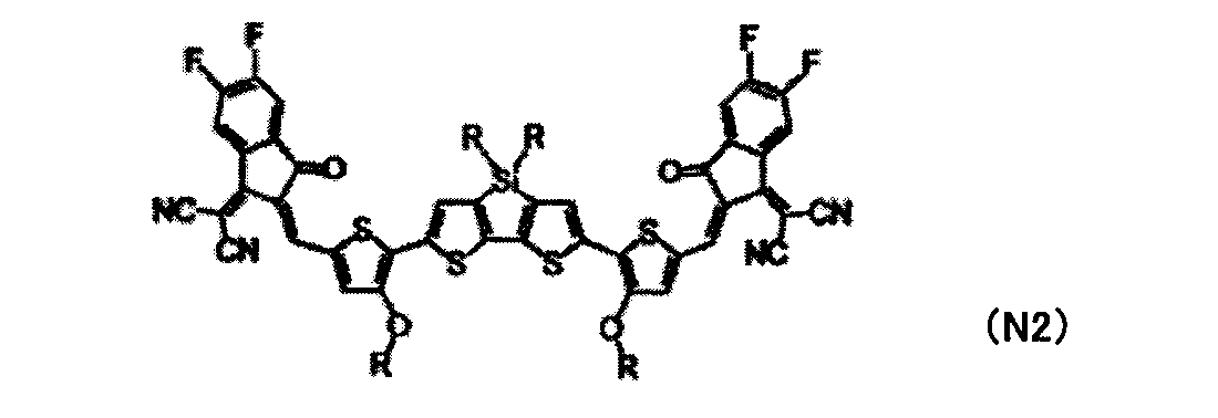
得られた光電変換層の上に、フラーレンC60(フロンティアカーボン社製)を膜厚40nmとなるように真空蒸着法を用いて形成し、電子輸送層とした。
その後、上記電子輸送層上に真空蒸着法を用いてアルミニウムを膜厚100nmとなるように形成して反射電極とした。
得られた有機フォトダイオードの分光感度の測定から、波長940nmにおいて-1Vでの印加電圧下の外部量子効率として38%の値が、また、単位面積当たりの暗電流密度は、1×10⁻⁷A/cm2の値が得られた。
<比較例1>
正孔輸送層を成膜しなかった以外は実施例1と同様に有機フォトダイオードを得た。
この有機フォトダイオードは、波長940nmにおいて-1Vでの印加電圧下では漏れ電流量が大きいために外部量子効率は正確に計測できなかった。また、単位面積当たりの暗電流密度は、2×10⁻³A/cm2であった。
正孔輸送層を成膜しなかった以外は実施例1と同様に有機フォトダイオードを得た。
この有機フォトダイオードは、波長940nmにおいて-1Vでの印加電圧下では漏れ電流量が大きいために外部量子効率は正確に計測できなかった。また、単位面積当たりの暗電流密度は、2×10⁻³A/cm2であった。
<比較例2>
正孔輸送層を市販のPEDOT:PSS(Clevios P VP AI4083、Heraeus社製)で成膜した以外は実施例1と同様に有機フォトダイオードを得た。
この有機フォトダイオードは、波長940nmにおいて-1Vでの印加電圧下の外部量子効率として、36%の値が、また、単位面積当たりの暗電流密度は、3×10⁻⁷A/cm2の値が得られた。
正孔輸送層を市販のPEDOT:PSS(Clevios P VP AI4083、Heraeus社製)で成膜した以外は実施例1と同様に有機フォトダイオードを得た。
この有機フォトダイオードは、波長940nmにおいて-1Vでの印加電圧下の外部量子効率として、36%の値が、また、単位面積当たりの暗電流密度は、3×10⁻⁷A/cm2の値が得られた。
実施例1及び比較例1,2の結果を表1にまとめた。

<実施例2>
以下の方法により、有機フォトダイオードを作製した。
ガラス基板の上にインジウム・スズ酸化物(ITO)透明導電膜を130nm成膜したもの(スパッタ成膜品、シート抵抗15Ω)を通常のフォトリソグラフィ技術により2mm幅のストライプにパターニングして透明電極を形成した。パターン形成したITO基板を、超純水、アセトン、イソプロピルアルコールの順番で超音波洗浄により洗浄後、窒素ブローで乾燥させ、最後に紫外線オゾン洗浄を行った。
以下の方法により、有機フォトダイオードを作製した。
ガラス基板の上にインジウム・スズ酸化物(ITO)透明導電膜を130nm成膜したもの(スパッタ成膜品、シート抵抗15Ω)を通常のフォトリソグラフィ技術により2mm幅のストライプにパターニングして透明電極を形成した。パターン形成したITO基板を、超純水、アセトン、イソプロピルアルコールの順番で超音波洗浄により洗浄後、窒素ブローで乾燥させ、最後に紫外線オゾン洗浄を行った。
まず、下記式(H1)に示すポリマー(Mw=85000、Mn=60000、Mw/Mn=1.4)4mgを1mLのトルエンに溶解させ、正孔輸送層形成用組成物を調製した。この組成物を窒素雰囲気下において1500rpmで30秒間、ITO基板の電極面にスピンコートし、230℃で1時間加熱乾燥して、膜厚25nmの正孔輸送層を形成した。
なお、下記式(H1)において、0.95の比率で含まれる繰り返し単位中のArは、下に0.95と記載されている9,9-ジn-ヘキシル-2-フルオレニル基であり、ランダムに0.95:0.05の割合で含まれているわけではない。0.05の繰り返し単位についても同様である。
なお、下記式(H1)において、0.95の比率で含まれる繰り返し単位中のArは、下に0.95と記載されている9,9-ジn-ヘキシル-2-フルオレニル基であり、ランダムに0.95:0.05の割合で含まれているわけではない。0.05の繰り返し単位についても同様である。
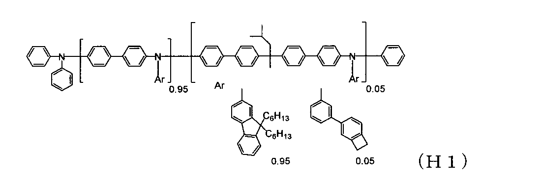
引き続き、下記式(P1)に示す化合物8mg、下記式(N1)に示す化合物12mgにクロロベンゼン0.98mL、1,8-ジヨードオクタン0.02mLを加えて溶解させ、光電変換層形成用組成物を調製した。この組成物を窒素雰囲気下において2500rpmで60秒間、上記正孔輸送層上にスピンコートして、膜厚100nmの光電変換層を形成した。
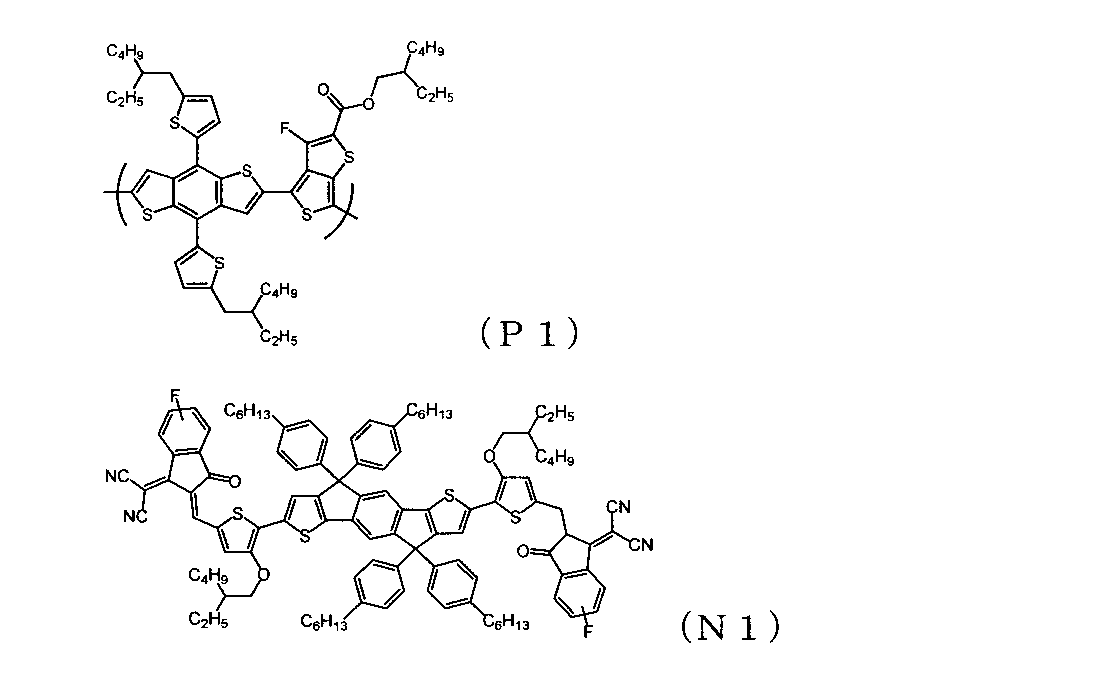
得られた光電変換層の上に、フラーレンC60(フロンティアカーボン社製)を膜厚40nmとなるように真空蒸着法を用いて形成し、電子輸送層とした。
その後、上記電子輸送層上に真空蒸着法を用いてアルミニウムを膜厚100nmとなるように、透明電極であるITOストライプと直交する2mm幅のストライプ形状に形成して反射電極とした。
以上の様にして、2mm×2mmのサイズの受光面積部分を有する有機フォトダイオードが得られた。
以上の様にして、2mm×2mmのサイズの受光面積部分を有する有機フォトダイオードが得られた。
得られた有機フォトダイオードの暗電流密度及び光電変換効率の測定結果は表2に示す通りであった。
<実施例3>
正孔輸送層を以下の方法で形成したほかは、実施例2と同様にして有機フォトダイオードを作製した。
正孔輸送層を以下の方法で形成したほかは、実施例2と同様にして有機フォトダイオードを作製した。
下記式(H2)に示すポリマー(Mw=34000、Mn=23000、Mw/Mn=1.5,式(1)数/1000=0.13)の4mgを1mLのトルエンに溶解させ、正孔輸送層形成用組成物を調製した。この組成物を窒素雰囲気下において1500rpmで30秒間ITO基板の電極面にスピンコートし、230℃で1時間加熱乾燥して、膜厚25nmの正孔輸送層を形成した。下記式(H2)のArはどちらの繰り返し単位においても9,9-ジn-ヘキシル-2-フルオレニル基である。

得られた有機フォトダイオードの暗電流密度及び光電変換効率の測定結果は表2に示す通りであった。
<比較例3>
以下の方法により、有機フォトダイオードを作製した。
以下の方法により、有機フォトダイオードを作製した。
まず、ジエチル亜鉛の15重量%トルエン溶液(シグマアルドリッチ製)をテトラヒドロフランで体積比1:2となるように希釈した組成物を窒素雰囲気下において調製した。この組成物を大気中に取り出し、実施例2と同様にして準備したITO基板上に4000rpmで30秒間スピンコートを行い、110℃で20分間乾燥させて酸化亜鉛に変換し、膜厚40nmの電子輸送層を形成した。
引き続き光電変換層を、実施例2と同様にして形成した。
得られた光電変換層の上に、三酸化モリブデンを膜厚7nmとなるように真空蒸着法を用いて形成し、正孔輸送層とした。
その後、真空蒸着法を用いて銀を膜厚100nmとなるように、透明電極であるITOストライプと直交する2mm幅のストライプ形状に形成して反射電極とした。
以上の様にして、2mm×2mmのサイズの受光面積部分を有するフォトダイオードが得られた。
得られた光電変換層の上に、三酸化モリブデンを膜厚7nmとなるように真空蒸着法を用いて形成し、正孔輸送層とした。
その後、真空蒸着法を用いて銀を膜厚100nmとなるように、透明電極であるITOストライプと直交する2mm幅のストライプ形状に形成して反射電極とした。
以上の様にして、2mm×2mmのサイズの受光面積部分を有するフォトダイオードが得られた。
得られた有機フォトダイオードの暗電流密度及び光電変換効率の測定結果は表2に示す通りであった。
<比較例4>
光電変換層を形成した後、正孔輸送層を形成する際、下記式(H3)に示す化合物を真空蒸着法を用いて20nmの膜厚に形成し、その後三酸化モリブデンを真空蒸着することで、化合物(H3)と三酸化モリブデンの二層の正孔輸送層としたほかは、比較例3と同様にしてフォトダイオードを作製した。
光電変換層を形成した後、正孔輸送層を形成する際、下記式(H3)に示す化合物を真空蒸着法を用いて20nmの膜厚に形成し、その後三酸化モリブデンを真空蒸着することで、化合物(H3)と三酸化モリブデンの二層の正孔輸送層としたほかは、比較例3と同様にしてフォトダイオードを作製した。
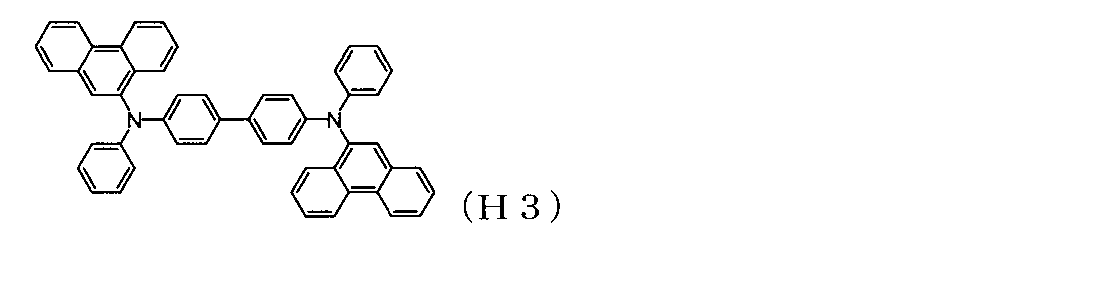
得られた有機フォトダイオードの暗電流密度及び光電変換効率の測定結果は表2に示す通りであった。
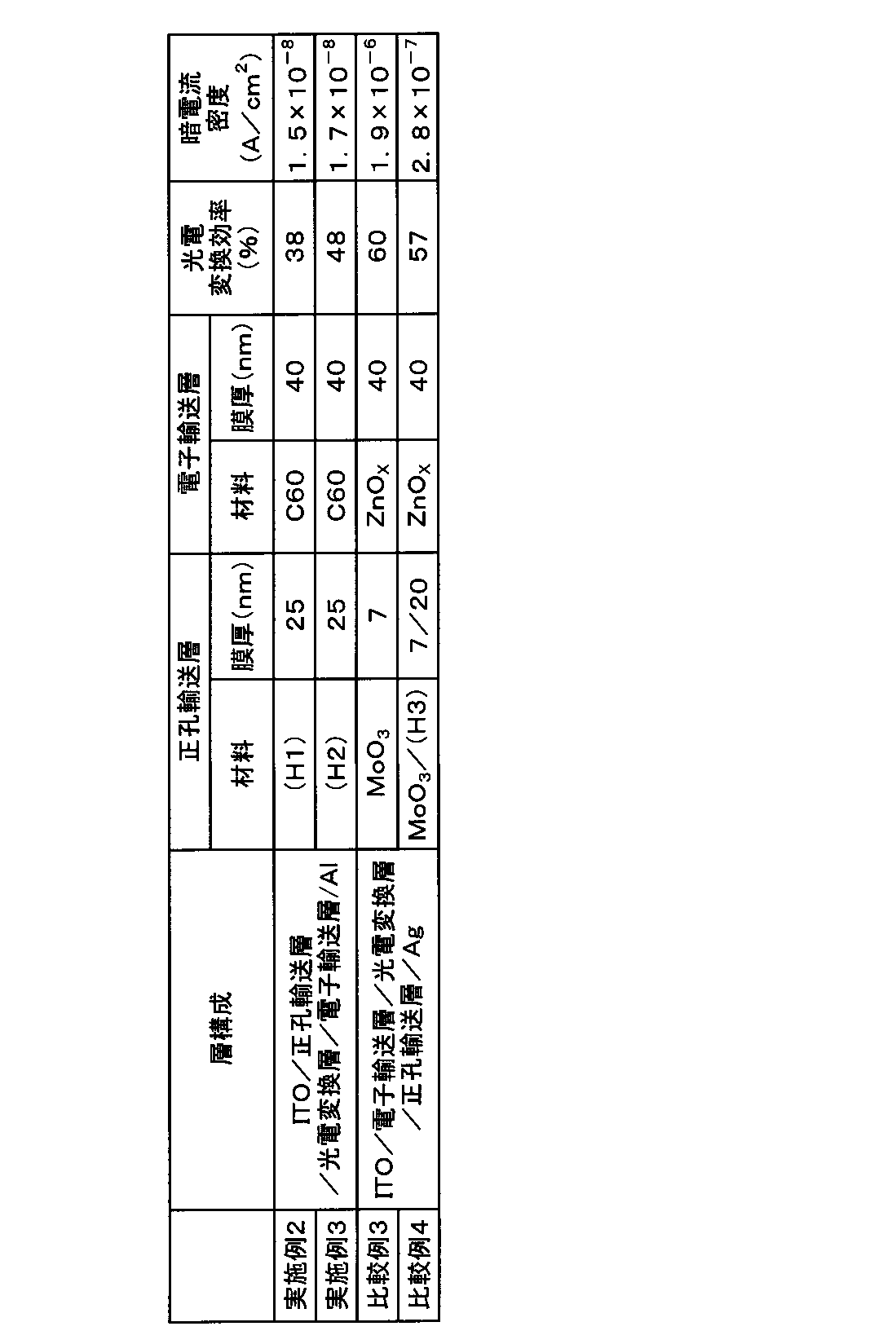
表1,2から明らかなとおり、本発明の有機フォトダイオードは、光電変換効率を維持した上で暗電流を大幅に低減できている。
本発明を特定の態様を用いて詳細に説明したが、本発明の意図と範囲を離れることなく様々な変更が可能であることは当業者に明らかである。
本出願は、2018年12月20日付で出願された日本特許出願2018-238473に基づいており、その全体が引用により援用される。
本出願は、2018年12月20日付で出願された日本特許出願2018-238473に基づいており、その全体が引用により援用される。
1 マクロレンズ
2 カラーフィルタ
3 保護膜
4 金属配線層
4A 金属配線
5 シリコン基板
6 トランジスタ
7 信号蓄積部
10 有機フォトダイオード
11 第1電極
12 正孔輸送層
13 光電変換層
14 電子輸送層
15 第2電極
20 有機光電膜
2 カラーフィルタ
3 保護膜
4 金属配線層
4A 金属配線
5 シリコン基板
6 トランジスタ
7 信号蓄積部
10 有機フォトダイオード
11 第1電極
12 正孔輸送層
13 光電変換層
14 電子輸送層
15 第2電極
20 有機光電膜
Claims (13)
- 第1電極、正孔輸送層、光電変換層、及び第2電極をこの順に含んでなる有機フォトダイオードであって、
該光電変換層がp型半導体とn型半導体を含み、
該正孔輸送層が、下記式(2)で表される繰り返し単位を含む高分子化合物を含有し、
該高分子化合物が、該高分子化合物間において230℃において互いに側鎖の炭素原子に結合する基を有することを特徴とする有機フォトダイオード。

Ar11及びAr12は、各々独立して、直接結合、置換基を有していてもよい芳香族炭化水素基又は置換基を有していてもよい芳香族複素環基を表す。
Ar13~Ar15は、各々独立に、置換基を有していてもよい芳香族炭化水素基又は置換基を有していてもよい芳香族複素環基を表す。
m個のAr14同士及びAr15同士は、各々、同じでもよく、異なっていてもよい。
但し、Ar11及びAr12が同時に直接結合であることはない。 - 前記230℃において互いに側鎖の炭素原子に結合する基が、下記式(1A)~(1I)のいずれかで表される基である請求項1に記載の有機フォトダイオード。

nは1~6の整数を表す。
n個のAr1は、同じでもよく、異なっていてもよく、式(1A)中のベンゾシクロブテン環は、置換基を有していてもよい。該置換基同士が、互いに結合して環を形成してもよい。
式(1B)~(1I)中、R3~R5は、水素原子又はアルキル基を表す。
R6、R7、R10は、水素原子、アルキル基又はアルコキシ基を表す。
r,jは1~5の整数、kは1~7の整数を表す。
rが2以上のとき、複数のR6は同じであっても異なっていてもよく、隣接するR6同士が結合して環を形成してもよい。
jが2以上のとき、複数のR7は同じであっても異なっていてもよく、隣接するR7同士が結合して環を形成してもよい。
kが2以上のとき、複数のR10は同じであっても異なっていてもよい。
Ar2は、置換基を有していてもよい芳香族炭化水素基又は置換基を有していてもよい芳香族複素環基を表す。 - 前記230℃において互いに側鎖の炭素原子に結合する基が、開環して重合する基である請求項1または2に記載の有機フォトダイオード。
- 前記n型半導体が下記式(4)で表される請求項1~請求項3のいずれか一項に記載の有機フォトダイオード。

- 前記n型半導体が下記式(5)で表される、請求項1~請求項4のいずれか一項に記載の有機フォトダイオード。

Ar42はそれぞれ独立に下記式(5a-2)~(5d-2)で表される。
Ar43はそれぞれ独立に下記式(5a-3)~(5d-3)で表される。
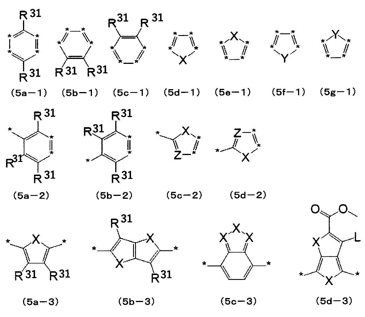
XはC=O、O、S、又はSeを表す。
YはCR31R31、SiR31R31、GeR31R31、NR31、又はC=Oを表す。
ZはCR31、又はNを表す。
LはR31、又はハロゲン原子を表す。
R31はそれぞれ独立に、水素原子、分岐を有していてもよい炭素数1~30のアルキル基、分岐を有していてもよい炭素数1~30のアルコキシ基、或いは分岐を有していてもよい炭素数1~30のアルキル基及び/又は分岐を有していてもよい炭素数1~30のアルコキシ基で置換されていてもよいフェニル基を表す。
Aはマロノニトリル基を有するアクセプター部位を表す。
x1は0又は1、x2は1~6の整数、x3は0又は1をそれぞれ表す。
式(5)において、式(5f-1)と式(5g-1)とが隣接することはない。 - 前記Aのマロノニトリル基を有するアクセプター部位が、下記式(5A)~(5C)のいずれかで表される請求項4又は5に記載の有機フォトダイオード。
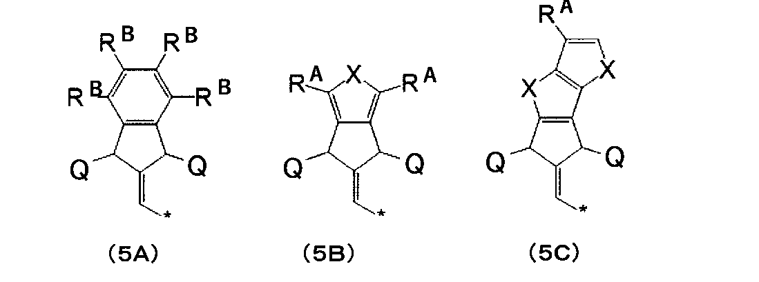
Qはマロノニトリル基もしくはO=を表す。Qの少なくとも一方はマロノニトリル基である。
XはC=O、O、S、又はSeを表す。
RAはそれぞれ独立に、水素原子、ハロゲン原子、分岐を有していてもよい炭素数1~30のアルキル基、分岐を有していてもよい炭素数1~30のアルコキシ基、或いは分岐を有していてもよい炭素数1~30のアルキル基及び/又は分岐を有していてもよい炭素数1~30のアルコキシ基で置換されていてもよいフェニル基を表す。
RBはRAと同義であるか、或いは隣接するRB同士で芳香族6員環を形成する。 - 前記高分子化合物が、部分構造としてフルオレン環由来の1価又は2価以上の基を含む請求項1~請求項6のいずれか一項に記載の有機フォトダイオード。
- 前記高分子化合物の重量平均分子量(Mw)が20000以上であり、分散度(Mw/Mn)が2.5以下である(但し、Mnは数平均分子量を表す。)請求項1~請求項7のいずれか一項に記載の有機フォトダイオード。
- 前記高分子化合物が、下記式(3)で表される繰り返し単位を含む請求項1~請求項8のいずれか一項に記載の有機フォトダイオード。
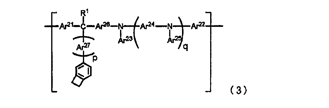
Ar21及びAr22は、各々独立して、直接結合、置換基を有していてもよい芳香族炭化水素基又は置換基を有していてもよい芳香族複素環基を表す。
Ar23~Ar27は、各々独立に、置換基を有していてもよい芳香族炭化水素基又は置換基を有していてもよい芳香族複素環基を表す。
R1は、水素原子、置換基を有していてもよい炭素数1~24のアルキル基、置換基を有していてもよい炭素数1~24のアルコキシ基、置換基を有してもよい芳香族炭化水素基又は置換基を有してもよい芳香族複素環基を表す。
p個のAr27は、同じでもよく、また異なっていてもよい。q個のAr24同士及びAr25同士は、各々、同じでもよく、異なっていてもよい。Ar21及びAr22が同時に直接結合であることはない。 - 前記高分子化合物が、前記式(1)で表される基を、分子量1000あたり0.01個以上、3個以下有する請求項1~請求項9のいずれか一項に記載の有機フォトダイオード。
- 前記n型半導体において、フラーレン骨格を有するn型半導体の割合が、フラーレン骨格を有さないn型半導体に対して10重量%以下である請求項1~請求項10のいずれか一項に記載の有機フォトダイオード。
- 前記n型半導体において、フラーレン骨格を有するものが実質的に含まれていない請求項1~請求項11のいずれか一項に記載の有機フォトダイオード。
- 請求項1~請求項12のいずれか一項に記載の有機フォトダイオードを含む赤外線CMOSセンサー。
Priority Applications (4)
| Application Number | Priority Date | Filing Date | Title |
|---|---|---|---|
| JP2020561543A JP7400734B2 (ja) | 2018-12-20 | 2019-12-20 | 有機フォトダイオード及び赤外線cmosセンサー |
| CN201980083476.7A CN113242874B (zh) | 2018-12-20 | 2019-12-20 | 有机光电二极管及红外cmos传感器 |
| EP19898449.4A EP3901194A4 (en) | 2018-12-20 | 2019-12-20 | ORGANIC PHOTODIODE AND INFRARED CMOS SENSOR |
| US17/348,221 US20210313516A1 (en) | 2018-12-20 | 2021-06-15 | Organic photodiode and infrared cmos sensor |
Applications Claiming Priority (2)
| Application Number | Priority Date | Filing Date | Title |
|---|---|---|---|
| JP2018238473 | 2018-12-20 | ||
| JP2018-238473 | 2018-12-20 |
Related Child Applications (1)
| Application Number | Title | Priority Date | Filing Date |
|---|---|---|---|
| US17/348,221 Continuation US20210313516A1 (en) | 2018-12-20 | 2021-06-15 | Organic photodiode and infrared cmos sensor |
Publications (1)
| Publication Number | Publication Date |
|---|---|
| WO2020130133A1 true WO2020130133A1 (ja) | 2020-06-25 |
Family
ID=71101313
Family Applications (1)
| Application Number | Title | Priority Date | Filing Date |
|---|---|---|---|
| PCT/JP2019/050075 Ceased WO2020130133A1 (ja) | 2018-12-20 | 2019-12-20 | 有機フォトダイオード及び赤外線cmosセンサー |
Country Status (5)
| Country | Link |
|---|---|
| US (1) | US20210313516A1 (ja) |
| EP (1) | EP3901194A4 (ja) |
| JP (1) | JP7400734B2 (ja) |
| CN (1) | CN113242874B (ja) |
| WO (1) | WO2020130133A1 (ja) |
Cited By (5)
| Publication number | Priority date | Publication date | Assignee | Title |
|---|---|---|---|---|
| JP2022030124A (ja) * | 2020-08-06 | 2022-02-18 | 三菱ケミカル株式会社 | 有機半導体デバイス、有機半導体インク及びフォトディテクタ |
| WO2024075810A1 (ja) * | 2022-10-05 | 2024-04-11 | 三菱ケミカル株式会社 | 有機光電変換膜、有機光電変換素子、有機光電変換膜の製造方法、及び有機半導体インク組成物 |
| JP2024057568A (ja) * | 2022-10-12 | 2024-04-24 | 采▲ぎょく▼科技股▲ふん▼有限公司 | イメージセンサ |
| WO2024177081A1 (ja) * | 2023-02-22 | 2024-08-29 | 三菱ケミカル株式会社 | 重合体、有機電界発光素子用組成物、有機電界発光素子、有機el表示装置及び有機el照明 |
| US12178056B2 (en) | 2020-10-28 | 2024-12-24 | Samsung Electronics Co., Ltd. | Sensor and electronic device |
Families Citing this family (2)
| Publication number | Priority date | Publication date | Assignee | Title |
|---|---|---|---|---|
| EP3809474B1 (en) * | 2019-10-18 | 2023-07-19 | Samsung Electronics Co., Ltd. | Quantum dot light-emitting device and electronic device |
| US12342650B2 (en) | 2022-04-04 | 2025-06-24 | Omnivision Technologies, Inc. | Near infrared to far infrared polarization sensitive image sensor |
Citations (14)
| Publication number | Priority date | Publication date | Assignee | Title |
|---|---|---|---|---|
| JPS59194393A (ja) | 1983-03-25 | 1984-11-05 | イ−ストマン コダツク カンパニ− | 改良された電力転換効率をもつ有機エレクトロルミネツセント装置 |
| JPH05331459A (ja) | 1992-04-03 | 1993-12-14 | Pioneer Electron Corp | 有機エレクトロルミネッセンス素子 |
| JPH06207169A (ja) | 1992-11-17 | 1994-07-26 | Idemitsu Kosan Co Ltd | 有機エレクトロルミネッセンス素子 |
| US5645948A (en) | 1996-08-20 | 1997-07-08 | Eastman Kodak Company | Blue organic electroluminescent devices |
| JP2001223084A (ja) | 2000-02-07 | 2001-08-17 | Junji Kido | 有機電界発光素子 |
| JP2003213002A (ja) | 2001-11-19 | 2003-07-30 | Mitsubishi Chemicals Corp | 芳香族ジアミン含有高分子化合物およびそれを用いる有機電界発光素子 |
| JP2004002740A (ja) | 2002-03-22 | 2004-01-08 | Mitsubishi Chemicals Corp | 高分子化合物、1,4−フェニレンジアミン誘導体、電荷輸送材料、有機電界発光素子材料および有機電界発光素子 |
| JP2009295974A (ja) * | 2008-05-07 | 2009-12-17 | Mitsubishi Chemicals Corp | 有機電界発光素子用組成物、高分子膜、有機電界発光素子、有機elディスプレイ及び有機el照明 |
| JP2012004578A (ja) | 2011-07-26 | 2012-01-05 | Fujifilm Corp | 光電変換素子、光電変換素子の製造方法、固体撮像素子 |
| JP2016134570A (ja) | 2015-01-21 | 2016-07-25 | パナソニックIpマネジメント株式会社 | 有機光電変換材料、光電変換素子および撮像装置 |
| JP2016225456A (ja) | 2015-05-29 | 2016-12-28 | パナソニックIpマネジメント株式会社 | 撮像装置および光電変換膜の製造方法 |
| WO2018065352A1 (en) * | 2016-10-05 | 2018-04-12 | Merck Patent Gmbh | Organic photodetector |
| WO2018066583A1 (ja) * | 2016-10-05 | 2018-04-12 | 三菱ケミカル株式会社 | イリジウム錯体化合物、並びに前記化合物を含有する組成物、有機電界発光素子、表示装置及び照明装置 |
| WO2018103496A1 (zh) * | 2016-12-07 | 2018-06-14 | 北京大学 | 多并稠环共轭大分子及其制备方法和应用 |
Family Cites Families (4)
| Publication number | Priority date | Publication date | Assignee | Title |
|---|---|---|---|---|
| CN102245543B (zh) * | 2009-10-30 | 2014-09-10 | 三菱化学株式会社 | 低分子化合物、聚合物、电子器件材料、电子器件用组合物、有机场致发光元件、有机太阳能电池元件、显示装置及照明装置 |
| US9929347B2 (en) * | 2012-03-27 | 2018-03-27 | Sumitomo Chemical Company, Limtied | Polymer compound and light emitting element using same |
| EP3333170B1 (en) * | 2016-12-06 | 2020-04-29 | Merck Patent GmbH | Asymmetrical polycyclic compounds for use in organic semiconductors |
| US11261291B2 (en) * | 2016-12-22 | 2022-03-01 | Merck Patent Gmbh | Materials for electronic devices |
-
2019
- 2019-12-20 EP EP19898449.4A patent/EP3901194A4/en active Pending
- 2019-12-20 CN CN201980083476.7A patent/CN113242874B/zh active Active
- 2019-12-20 JP JP2020561543A patent/JP7400734B2/ja active Active
- 2019-12-20 WO PCT/JP2019/050075 patent/WO2020130133A1/ja not_active Ceased
-
2021
- 2021-06-15 US US17/348,221 patent/US20210313516A1/en active Pending
Patent Citations (14)
| Publication number | Priority date | Publication date | Assignee | Title |
|---|---|---|---|---|
| JPS59194393A (ja) | 1983-03-25 | 1984-11-05 | イ−ストマン コダツク カンパニ− | 改良された電力転換効率をもつ有機エレクトロルミネツセント装置 |
| JPH05331459A (ja) | 1992-04-03 | 1993-12-14 | Pioneer Electron Corp | 有機エレクトロルミネッセンス素子 |
| JPH06207169A (ja) | 1992-11-17 | 1994-07-26 | Idemitsu Kosan Co Ltd | 有機エレクトロルミネッセンス素子 |
| US5645948A (en) | 1996-08-20 | 1997-07-08 | Eastman Kodak Company | Blue organic electroluminescent devices |
| JP2001223084A (ja) | 2000-02-07 | 2001-08-17 | Junji Kido | 有機電界発光素子 |
| JP2003213002A (ja) | 2001-11-19 | 2003-07-30 | Mitsubishi Chemicals Corp | 芳香族ジアミン含有高分子化合物およびそれを用いる有機電界発光素子 |
| JP2004002740A (ja) | 2002-03-22 | 2004-01-08 | Mitsubishi Chemicals Corp | 高分子化合物、1,4−フェニレンジアミン誘導体、電荷輸送材料、有機電界発光素子材料および有機電界発光素子 |
| JP2009295974A (ja) * | 2008-05-07 | 2009-12-17 | Mitsubishi Chemicals Corp | 有機電界発光素子用組成物、高分子膜、有機電界発光素子、有機elディスプレイ及び有機el照明 |
| JP2012004578A (ja) | 2011-07-26 | 2012-01-05 | Fujifilm Corp | 光電変換素子、光電変換素子の製造方法、固体撮像素子 |
| JP2016134570A (ja) | 2015-01-21 | 2016-07-25 | パナソニックIpマネジメント株式会社 | 有機光電変換材料、光電変換素子および撮像装置 |
| JP2016225456A (ja) | 2015-05-29 | 2016-12-28 | パナソニックIpマネジメント株式会社 | 撮像装置および光電変換膜の製造方法 |
| WO2018065352A1 (en) * | 2016-10-05 | 2018-04-12 | Merck Patent Gmbh | Organic photodetector |
| WO2018066583A1 (ja) * | 2016-10-05 | 2018-04-12 | 三菱ケミカル株式会社 | イリジウム錯体化合物、並びに前記化合物を含有する組成物、有機電界発光素子、表示装置及び照明装置 |
| WO2018103496A1 (zh) * | 2016-12-07 | 2018-06-14 | 北京大学 | 多并稠环共轭大分子及其制备方法和应用 |
Non-Patent Citations (10)
Cited By (6)
| Publication number | Priority date | Publication date | Assignee | Title |
|---|---|---|---|---|
| JP2022030124A (ja) * | 2020-08-06 | 2022-02-18 | 三菱ケミカル株式会社 | 有機半導体デバイス、有機半導体インク及びフォトディテクタ |
| US12178056B2 (en) | 2020-10-28 | 2024-12-24 | Samsung Electronics Co., Ltd. | Sensor and electronic device |
| WO2024075810A1 (ja) * | 2022-10-05 | 2024-04-11 | 三菱ケミカル株式会社 | 有機光電変換膜、有機光電変換素子、有機光電変換膜の製造方法、及び有機半導体インク組成物 |
| JP2024057568A (ja) * | 2022-10-12 | 2024-04-24 | 采▲ぎょく▼科技股▲ふん▼有限公司 | イメージセンサ |
| JP7578757B2 (ja) | 2022-10-12 | 2024-11-06 | 采▲ぎょく▼科技股▲ふん▼有限公司 | イメージセンサ |
| WO2024177081A1 (ja) * | 2023-02-22 | 2024-08-29 | 三菱ケミカル株式会社 | 重合体、有機電界発光素子用組成物、有機電界発光素子、有機el表示装置及び有機el照明 |
Also Published As
| Publication number | Publication date |
|---|---|
| JP7400734B2 (ja) | 2023-12-19 |
| CN113242874B (zh) | 2023-12-12 |
| CN113242874A (zh) | 2021-08-10 |
| EP3901194A4 (en) | 2022-03-02 |
| US20210313516A1 (en) | 2021-10-07 |
| JPWO2020130133A1 (ja) | 2021-10-28 |
| EP3901194A1 (en) | 2021-10-27 |
Similar Documents
| Publication | Publication Date | Title |
|---|---|---|
| JP7400734B2 (ja) | 有機フォトダイオード及び赤外線cmosセンサー | |
| JP6791311B2 (ja) | 重合体、有機電界発光素子用組成物、有機電界発光素子、有機el表示装置及び有機el照明 | |
| CN104411743B (zh) | 高分子化合物、电荷传输性聚合物、有机电致发光元件用组合物、有机电致发光元件、有机el显示装置及有机el照明 | |
| KR101830985B1 (ko) | 저분자 화합물, 중합체, 전자 디바이스 재료, 전자 디바이스용 조성물, 유기 전계 발광 소자, 유기 태양 전지 소자, 표시 장치 및 조명 장치 | |
| KR20110051186A (ko) | 중합체, 발광층 재료, 유기 전계 발광 소자 재료, 유기 전계 발광 소자용 조성물, 이들을 이용한 유기 전계 발광 소자, 태양 전지 소자, 유기 el 표시 장치, 및 유기 el 조명 | |
| US20170044308A1 (en) | Polymer or oligomer, hole transport material composition, and organic electronic element using same | |
| JP7044063B2 (ja) | 有機エレクトロニクス材料及びその利用 | |
| TW201631815A (zh) | 光電轉換元件及使用其的影像感測器 | |
| JP6782418B2 (ja) | 有機エレクトロニクス材料及びその利用 | |
| JP2024054634A (ja) | 有機光電変換素子の製造方法及び有機光電変換素子 | |
| KR20190116289A (ko) | 유기 일렉트로닉스 재료, 유기 일렉트로닉스 소자 및 유기 일렉트로루미네센스 소자 | |
| Wu et al. | Side chain engineering of naphthalene diimide–bithiophene‐based polymer acceptors in all‐polymer solar cells | |
| KR20210133896A (ko) | 적외선 흡수용 고분자, 적외선 흡수/차단 필름, 광전 소자, 센서 및 전자 장치 | |
| WO2023157864A1 (ja) | 有機半導体インク、有機膜、光電変換層、光電変換層の製造方法及び有機光電変換素子 | |
| EP3859806A1 (en) | Organic electronic material and organic electronic element | |
| WO2023058724A1 (ja) | 組成物及びインク組成物 | |
| Liang et al. | Supramolecular assembly of H‐bonded side‐chain polymers containing conjugated pyridyl H‐acceptor pendants and various low‐band‐gap H‐donor dyes bearing cyanoacrylic acid groups for organic solar cell applications | |
| WO2021161793A1 (ja) | 高分子化合物、組成物、インク、及び光電変換素子 | |
| TW202340395A (zh) | 有機半導體墨水、光電轉換層及有機光電轉換元件 | |
| JP2024116851A (ja) | 有機半導体インク、光電変換層及び有機光電変換素子 | |
| JP6657663B2 (ja) | 電荷輸送性材料、該材料を用いたインク組成物、有機エレクトロニクス素子、有機エレクトロルミネセンス素子、表示素子、表示装置及び照明装置 | |
| JP2023057055A (ja) | 組成物及びインク組成物 | |
| WO2025100273A1 (ja) | 化合物、組成物、インク、光電変換素子、及び光センサー | |
| WO2024075810A1 (ja) | 有機光電変換膜、有機光電変換素子、有機光電変換膜の製造方法、及び有機半導体インク組成物 | |
| WO2025150466A1 (ja) | 光電変換素子及び光センサー |
Legal Events
| Date | Code | Title | Description |
|---|---|---|---|
| 121 | Ep: the epo has been informed by wipo that ep was designated in this application |
Ref document number: 19898449 Country of ref document: EP Kind code of ref document: A1 |
|
| ENP | Entry into the national phase |
Ref document number: 2020561543 Country of ref document: JP Kind code of ref document: A |
|
| NENP | Non-entry into the national phase |
Ref country code: DE |
|
| ENP | Entry into the national phase |
Ref document number: 2019898449 Country of ref document: EP Effective date: 20210720 |