WO2020130133A1 - Photodiode organique et capteur cmos infrarouge - Google Patents
Photodiode organique et capteur cmos infrarouge Download PDFInfo
- Publication number
- WO2020130133A1 WO2020130133A1 PCT/JP2019/050075 JP2019050075W WO2020130133A1 WO 2020130133 A1 WO2020130133 A1 WO 2020130133A1 JP 2019050075 W JP2019050075 W JP 2019050075W WO 2020130133 A1 WO2020130133 A1 WO 2020130133A1
- Authority
- WO
- WIPO (PCT)
- Prior art keywords
- group
- substituent
- ring
- organic photodiode
- carbon atoms
- Prior art date
- Legal status (The legal status is an assumption and is not a legal conclusion. Google has not performed a legal analysis and makes no representation as to the accuracy of the status listed.)
- Ceased
Links
- 0 C*(C)c1c([C@@](*)C(C2*)=CC)c2c(*)c(*)c1* Chemical compound C*(C)c1c([C@@](*)C(C2*)=CC)c2c(*)c(*)c1* 0.000 description 6
- RKJHJMAZNPASHY-UHFFFAOYSA-N Cc(cc1C2)ccc1-c1c2cccc1 Chemical compound Cc(cc1C2)ccc1-c1c2cccc1 RKJHJMAZNPASHY-UHFFFAOYSA-N 0.000 description 1
- GRVMBGBDPRLWLA-UHFFFAOYSA-N Cc1cc(-c2ccc(CC3)c3c2)ccc1 Chemical compound Cc1cc(-c2ccc(CC3)c3c2)ccc1 GRVMBGBDPRLWLA-UHFFFAOYSA-N 0.000 description 1
Images
Classifications
-
- H—ELECTRICITY
- H10—SEMICONDUCTOR DEVICES; ELECTRIC SOLID-STATE DEVICES NOT OTHERWISE PROVIDED FOR
- H10F—INORGANIC SEMICONDUCTOR DEVICES SENSITIVE TO INFRARED RADIATION, LIGHT, ELECTROMAGNETIC RADIATION OF SHORTER WAVELENGTH OR CORPUSCULAR RADIATION
- H10F39/00—Integrated devices, or assemblies of multiple devices, comprising at least one element covered by group H10F30/00, e.g. radiation detectors comprising photodiode arrays
- H10F39/10—Integrated devices
- H10F39/12—Image sensors
- H10F39/191—Photoconductor image sensors
-
- C—CHEMISTRY; METALLURGY
- C08—ORGANIC MACROMOLECULAR COMPOUNDS; THEIR PREPARATION OR CHEMICAL WORKING-UP; COMPOSITIONS BASED THEREON
- C08G—MACROMOLECULAR COMPOUNDS OBTAINED OTHERWISE THAN BY REACTIONS ONLY INVOLVING UNSATURATED CARBON-TO-CARBON BONDS
- C08G73/00—Macromolecular compounds obtained by reactions forming a linkage containing nitrogen with or without oxygen or carbon in the main chain of the macromolecule, not provided for in groups C08G12/00 - C08G71/00
- C08G73/02—Polyamines
-
- C—CHEMISTRY; METALLURGY
- C08—ORGANIC MACROMOLECULAR COMPOUNDS; THEIR PREPARATION OR CHEMICAL WORKING-UP; COMPOSITIONS BASED THEREON
- C08G—MACROMOLECULAR COMPOUNDS OBTAINED OTHERWISE THAN BY REACTIONS ONLY INVOLVING UNSATURATED CARBON-TO-CARBON BONDS
- C08G73/00—Macromolecular compounds obtained by reactions forming a linkage containing nitrogen with or without oxygen or carbon in the main chain of the macromolecule, not provided for in groups C08G12/00 - C08G71/00
- C08G73/02—Polyamines
- C08G73/026—Wholly aromatic polyamines
-
- H—ELECTRICITY
- H10—SEMICONDUCTOR DEVICES; ELECTRIC SOLID-STATE DEVICES NOT OTHERWISE PROVIDED FOR
- H10K—ORGANIC ELECTRIC SOLID-STATE DEVICES
- H10K30/00—Organic devices sensitive to infrared radiation, light, electromagnetic radiation of shorter wavelength or corpuscular radiation
- H10K30/30—Organic devices sensitive to infrared radiation, light, electromagnetic radiation of shorter wavelength or corpuscular radiation comprising bulk heterojunctions, e.g. interpenetrating networks of donor and acceptor material domains
-
- H—ELECTRICITY
- H10—SEMICONDUCTOR DEVICES; ELECTRIC SOLID-STATE DEVICES NOT OTHERWISE PROVIDED FOR
- H10K—ORGANIC ELECTRIC SOLID-STATE DEVICES
- H10K85/00—Organic materials used in the body or electrodes of devices covered by this subclass
- H10K85/10—Organic polymers or oligomers
- H10K85/111—Organic polymers or oligomers comprising aromatic, heteroaromatic, or aryl chains, e.g. polyaniline, polyphenylene or polyphenylene vinylene
-
- H—ELECTRICITY
- H10—SEMICONDUCTOR DEVICES; ELECTRIC SOLID-STATE DEVICES NOT OTHERWISE PROVIDED FOR
- H10K—ORGANIC ELECTRIC SOLID-STATE DEVICES
- H10K85/00—Organic materials used in the body or electrodes of devices covered by this subclass
- H10K85/10—Organic polymers or oligomers
- H10K85/111—Organic polymers or oligomers comprising aromatic, heteroaromatic, or aryl chains, e.g. polyaniline, polyphenylene or polyphenylene vinylene
- H10K85/113—Heteroaromatic compounds comprising sulfur or selene, e.g. polythiophene
-
- H—ELECTRICITY
- H10—SEMICONDUCTOR DEVICES; ELECTRIC SOLID-STATE DEVICES NOT OTHERWISE PROVIDED FOR
- H10K—ORGANIC ELECTRIC SOLID-STATE DEVICES
- H10K85/00—Organic materials used in the body or electrodes of devices covered by this subclass
- H10K85/10—Organic polymers or oligomers
- H10K85/141—Organic polymers or oligomers comprising aliphatic or olefinic chains, e.g. poly N-vinylcarbazol, PVC or PTFE
-
- H—ELECTRICITY
- H10—SEMICONDUCTOR DEVICES; ELECTRIC SOLID-STATE DEVICES NOT OTHERWISE PROVIDED FOR
- H10K—ORGANIC ELECTRIC SOLID-STATE DEVICES
- H10K85/00—Organic materials used in the body or electrodes of devices covered by this subclass
- H10K85/10—Organic polymers or oligomers
- H10K85/151—Copolymers
-
- H—ELECTRICITY
- H10—SEMICONDUCTOR DEVICES; ELECTRIC SOLID-STATE DEVICES NOT OTHERWISE PROVIDED FOR
- H10K—ORGANIC ELECTRIC SOLID-STATE DEVICES
- H10K85/00—Organic materials used in the body or electrodes of devices covered by this subclass
- H10K85/40—Organosilicon compounds, e.g. TIPS pentacene
-
- H—ELECTRICITY
- H10—SEMICONDUCTOR DEVICES; ELECTRIC SOLID-STATE DEVICES NOT OTHERWISE PROVIDED FOR
- H10K—ORGANIC ELECTRIC SOLID-STATE DEVICES
- H10K85/00—Organic materials used in the body or electrodes of devices covered by this subclass
- H10K85/60—Organic compounds having low molecular weight
- H10K85/615—Polycyclic condensed aromatic hydrocarbons, e.g. anthracene
- H10K85/626—Polycyclic condensed aromatic hydrocarbons, e.g. anthracene containing more than one polycyclic condensed aromatic rings, e.g. bis-anthracene
-
- H—ELECTRICITY
- H10—SEMICONDUCTOR DEVICES; ELECTRIC SOLID-STATE DEVICES NOT OTHERWISE PROVIDED FOR
- H10K—ORGANIC ELECTRIC SOLID-STATE DEVICES
- H10K85/00—Organic materials used in the body or electrodes of devices covered by this subclass
- H10K85/60—Organic compounds having low molecular weight
- H10K85/649—Aromatic compounds comprising a hetero atom
- H10K85/655—Aromatic compounds comprising a hetero atom comprising only sulfur as heteroatom
-
- H—ELECTRICITY
- H10—SEMICONDUCTOR DEVICES; ELECTRIC SOLID-STATE DEVICES NOT OTHERWISE PROVIDED FOR
- H10K—ORGANIC ELECTRIC SOLID-STATE DEVICES
- H10K85/00—Organic materials used in the body or electrodes of devices covered by this subclass
- H10K85/60—Organic compounds having low molecular weight
- H10K85/649—Aromatic compounds comprising a hetero atom
- H10K85/657—Polycyclic condensed heteroaromatic hydrocarbons
- H10K85/6576—Polycyclic condensed heteroaromatic hydrocarbons comprising only sulfur in the heteroaromatic polycondensed ring system, e.g. benzothiophene
-
- H—ELECTRICITY
- H10—SEMICONDUCTOR DEVICES; ELECTRIC SOLID-STATE DEVICES NOT OTHERWISE PROVIDED FOR
- H10K—ORGANIC ELECTRIC SOLID-STATE DEVICES
- H10K30/00—Organic devices sensitive to infrared radiation, light, electromagnetic radiation of shorter wavelength or corpuscular radiation
- H10K30/20—Organic devices sensitive to infrared radiation, light, electromagnetic radiation of shorter wavelength or corpuscular radiation comprising organic-organic junctions, e.g. donor-acceptor junctions
-
- H—ELECTRICITY
- H10—SEMICONDUCTOR DEVICES; ELECTRIC SOLID-STATE DEVICES NOT OTHERWISE PROVIDED FOR
- H10K—ORGANIC ELECTRIC SOLID-STATE DEVICES
- H10K39/00—Integrated devices, or assemblies of multiple devices, comprising at least one organic radiation-sensitive element covered by group H10K30/00
- H10K39/30—Devices controlled by radiation
- H10K39/32—Organic image sensors
-
- Y—GENERAL TAGGING OF NEW TECHNOLOGICAL DEVELOPMENTS; GENERAL TAGGING OF CROSS-SECTIONAL TECHNOLOGIES SPANNING OVER SEVERAL SECTIONS OF THE IPC; TECHNICAL SUBJECTS COVERED BY FORMER USPC CROSS-REFERENCE ART COLLECTIONS [XRACs] AND DIGESTS
- Y02—TECHNOLOGIES OR APPLICATIONS FOR MITIGATION OR ADAPTATION AGAINST CLIMATE CHANGE
- Y02E—REDUCTION OF GREENHOUSE GAS [GHG] EMISSIONS, RELATED TO ENERGY GENERATION, TRANSMISSION OR DISTRIBUTION
- Y02E10/00—Energy generation through renewable energy sources
- Y02E10/50—Photovoltaic [PV] energy
- Y02E10/549—Organic PV cells
Definitions
- the present invention relates to an organic photodiode (organic photoelectric conversion element) and an infrared CMOS sensor using this organic photodiode. Specifically, the present invention relates to an organic photodiode that achieves both high photoelectric conversion efficiency and low dark current value, and an infrared CMOS sensor that uses this organic photodiode.
- CMOS image sensors are used as image sensors in digital cameras and smartphones.
- the CMOS sensor has a high sensitivity that can be photographed even in a low illuminance, a high dynamic range that can simultaneously capture a mixture of bright and dark images, a simultaneous exposure batch readout (global shutter) function, and a high frame that can track a fast-moving subject. Rates are required.
- the organic photoelectric conversion film is considered to be suitable for CMOS sensor applications from the following points. -Compared to Si photodiodes, they can be made thinner, allowing a wider incident angle and reliably photoelectrically converting a small amount of light. Since the signal storage thick photoelectric conversion unit can be designed independently, the capacity of the signal storage unit can be increased and a high dynamic range can be easily achieved. -The signal storage unit can be used as it is as a memory.
- CMOS sensors using organic photoelectric conversion films have expanded in recent years. There, by using an image different from the image by visible light, especially by using near-infrared rays, it is possible to detect a person on a night road that is difficult to see with the naked eye, or to confirm the crop harvest level from the image of the field, or simply with the naked eye. It is expected to be applied to security applications such as seeing the opposite side through a wall that can only be seen in black. This is because it is said that it is preferable to use the organic photoelectric conversion film because the sensor using silicon has low infrared sensitivity.
- a CMOS sensor using an organic photoelectric conversion film can be thinned, but on the other hand, problems such as short-circuiting of elements and leakage current (dark current) that occur due to thinning occur.
- the smoothing of the electrode exerts a great effect. For example, by providing a coating film on the electrodes, a short circuit preventing effect is obtained.
- the photoelectric conversion layer When the photoelectric conversion layer is divided into a layer having substantially only a p-type semiconductor and a layer having substantially only an n-type semiconductor, the dark current can be suppressed to a low value. It becomes less efficient.
- the photoelectric conversion efficiency is excellent, but there is a problem of dark current generation.
- Non-Patent Document 1 reports on the relationship between the dark current and the Ip difference between the hole blocking layer and the photoelectric conversion layer (quinacridone).
- the dark current density is reduced to about 1 ⁇ 10 ⁇ 7 A/cm 2 due to the presence of the blocking layer.
- Patent Document 1 a structure in which a current blocking layer (a hole blocking layer and an electron blocking layer) is provided on both surfaces of a photoelectric conversion layer is also proposed.
- the dark current density in Patent Document 1 is about 1 ⁇ 10 ⁇ 7 A/cm 2 even at a low level, and it has not reached the level currently required.
- the electron blocking layer 5 has a lower energy level HOMO and a higher energy level LUMO than the p-type semiconductor layer 7 of the photoelectric conversion layer 3'.
- the photoelectric conversion layer 3' is equivalent to the electron blocking layer 5".
- the hole blocking layer 6 is provided to reduce dark current due to holes injected from the upper electrode 4, and prevents holes from the upper electrode 4 from being injected into the photoelectric conversion layer 3. To do.
- hole blocking layer is effective in reducing the dark current, but specific examples of the hole blocking layer are described in the paragraph [0042], "hole blocking layer.” 6 is preferably an organic substance such as copper phthalocyanine, PTCDA, an acetylacetonate complex, BCP or Alq, an organic-metal compound, or an inorganic substance such as MgAg or MgO.”
- Patent Document 3 also discloses a structure in which blocking layers are provided on both surfaces of a photoelectric conversion layer.
- the dark current value is small but the efficiency is low, and 10% in the infrared region. It's just a degree.
- the efficiency is good, but the dark current value is ⁇ 1 V, 1 ⁇ 10 ⁇ 5 A/cm 2 to 1 ⁇ 10 ⁇ 6. Very high at about A/cm 2 .
- An object of the present invention is to provide an organic photodiode capable of reducing a dark current value while maintaining high photoelectric conversion efficiency, and an infrared CMOS sensor using this organic photodiode.
- the present inventor compares photoelectric conversion efficiencies by providing a photoelectric conversion layer with a bulk heterojunction structure containing a p-type semiconductor and an n-type semiconductor and then providing a hole transport layer containing a specific polymer compound as a blocking layer. It has succeeded in suppressing the dark current density to 10 ⁇ 7 A/cm 2 or less while maintaining a relatively high state. That is, the gist of the present invention is as follows.
- An organic photodiode including a first electrode, a hole transport layer, a photoelectric conversion layer, and a second electrode in this order, wherein the photoelectric conversion layer includes a p-type semiconductor and an n-type semiconductor,
- the pore transport layer contains a polymer compound containing a repeating unit represented by the following formula (2), and the polymer compound has a group in which carbon atoms of side chains are mutually bonded at 230° C. between the polymer compounds.
- An organic photodiode comprising:
- m represents an integer of 0 to 3.
- Ar 11 and Ar 12 each independently represent a direct bond, an aromatic hydrocarbon group which may have a substituent or an aromatic heterocyclic group which may have a substituent.
- Ar 13 to Ar 15 each independently represent an aromatic hydrocarbon group which may have a substituent or an aromatic heterocyclic group which may have a substituent.
- the m Ar 14s and the Ar 15s may be the same or different. However, Ar 11 and Ar 12 are not a direct bond at the same time.
- Ar 1 represents an aromatic hydrocarbon group which may have a substituent or an aromatic heterocyclic group which may have a substituent.
- n represents an integer of 1 to 6.
- the n Ar 1 s may be the same or different, and the benzocyclobutene ring in formula (1A) may have a substituent.
- the substituents may combine with each other to form a ring.
- R 3 to R 5 represent a hydrogen atom or an alkyl group.
- R 6 , R 7 and R 10 represent a hydrogen atom, an alkyl group or an alkoxy group.
- r and j are integers of 1 to 5, and k is an integer of 1 to 7.
- R 6 s When r is 2 or more, plural R 6 s may be the same or different, and adjacent R 6 s may be bonded to each other to form a ring.
- R 7 s When j is 2 or more, plural R 7 s may be the same or different, and adjacent R 7 s may be bonded to each other to form a ring.
- k is 2 or more, a plurality of R 10's may be the same or different.
- Ar 2 represents an aromatic hydrocarbon group which may have a substituent or an aromatic heterocyclic group which may have a substituent.
- D represents a donor moiety having a polycyclic aromatic group.
- A represents an acceptor moiety having a malononitrile group.
- Ar 41 is independently represented by the following formulas (5a-1) to (5g-1).
- Ar 42 is independently represented by the following formulas (5a-2) to (5d-2).
- Ar 43 is independently represented by the following formulas (5a-3) to (5d-3).
- Y represents CR 31 R 31 , SiR 31 R 31 , GeR 31 R 31 , NR 31 , or C ⁇ O.
- Z represents CR 31 or N.
- L represents R 31 or a halogen atom.
- Each R 31 independently has a hydrogen atom, an optionally branched alkyl group having 1 to 30 carbon atoms, an optionally branched alkoxy group having 1 to 30 carbon atoms, or a branched one.
- A represents an acceptor moiety having a malononitrile group.
- x1 represents 0 or 1
- x2 represents an integer of 1 to 6
- x3 represents 0 or 1.
- Expression (5f-1) and Expression (5g-1) are not adjacent to each other.
- * represents a binding site.
- Each R A independently represents a hydrogen atom, a halogen atom, an optionally branched alkyl group having 1 to 30 carbon atoms, an optionally branched alkoxy group having 1 to 30 carbon atoms, or a branched chain. It represents a phenyl group which may be substituted with an optionally substituted alkyl group having 1 to 30 carbon atoms and/or an optionally branched alkoxy group having 1 to 30 carbon atoms.
- R B has the same meaning as R A , or adjacent R B forms an aromatic 6-membered ring.
- the polymer compound has a weight average molecular weight (Mw) of 20,000 or more and a dispersity (Mw/Mn) of 2.5 or less (where Mn represents a number average molecular weight) [1] to The organic photodiode according to any one of [7].
- p represents an integer of 1 or more and 6 or less
- q represents an integer of 0 or more and 3 or less.
- Ar 21 and Ar 22 each independently represent a direct bond, an aromatic hydrocarbon group which may have a substituent or an aromatic heterocyclic group which may have a substituent.
- Ar 23 to Ar 27 each independently represent an aromatic hydrocarbon group which may have a substituent or an aromatic heterocyclic group which may have a substituent.
- R 1 is a hydrogen atom, an alkyl group having 1 to 24 carbon atoms which may have a substituent, an alkoxy group having 1 to 24 carbon atoms which may have a substituent, or a substituent. It represents a good aromatic hydrocarbon group or an aromatic heterocyclic group which may have a substituent.
- the p Ar 27 s may be the same or different.
- the q Ar 24's and Ar 25's may be the same or different.
- Ar 21 and Ar 22 are not direct bonds at the same time.
- the proportion of the n-type semiconductor having a fullerene skeleton is 10% by weight or less with respect to the n-type semiconductor having no fullerene skeleton, [1] to [10] Organic photodiode.
- an organic photodiode having a high photoelectric conversion efficiency and a low dark current value.
- a high performance infrared CMOS sensor can be provided using the organic photodiode of the present invention.
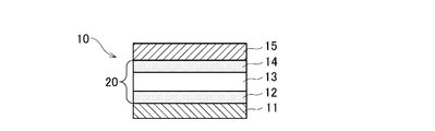
- FIG. 1 is a schematic cross-sectional view showing an example of the embodiment of the organic photodiode of the present invention.
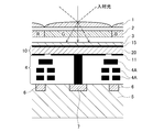
- FIG. 2 is a schematic cross-sectional view showing an example of the structure of the infrared CMOS sensor of the present invention using the organic photodiode of the present invention.
- the organic photodiode of the present invention is an organic photodiode including a first electrode, a hole transport layer, a photoelectric conversion layer, and a second electrode in this order, wherein the photoelectric conversion layer is a p-type semiconductor and an n-type semiconductor.
- the hole transport layer contains a polymer compound containing a repeating unit represented by the following formula (2), and the polymer compounds have side chains at 230° C. between the polymer compounds. It has a group bonded to the carbon atom of.
- a polymer compound containing a repeating unit represented by the following formula (2) which also includes a hole transport layer according to the present invention, wherein carbon atoms of side chains between the polymer compounds are 230°C.
- the polymer compound having a group that binds to may be referred to as the “hole transporting polymer of the present invention”.
- m represents an integer of 0 to 3.
- Ar 11 and Ar 12 each independently represent a direct bond, an aromatic hydrocarbon group which may have a substituent or an aromatic heterocyclic group which may have a substituent.
- Ar 13 to Ar 15 each independently represent an aromatic hydrocarbon group which may have a substituent or an aromatic heterocyclic group which may have a substituent.
- the m Ar 14s and the Ar 15s may be the same or different. However, Ar 11 and Ar 12 are not a direct bond at the same time.
- FIG. 1 is a schematic sectional view showing an example of the organic photodiode of the present invention.
- a first electrode 11, a hole transport layer 12, a photoelectric conversion layer 13, an electron transport layer 14, and a second electrode 15 as a lower electrode are laminated in this order.
- the hole transport layer 12, the photoelectric conversion layer 13, and the electron transport layer 14 form the organic photoelectric film 20.
- a substrate is provided on the side of the first electrode 11 opposite to the hole transport layer 12. It is preferable to provide the hole transport layer according to the present invention on the first electrode formed on the substrate because the smoothness of the substrate affects the hole transport layer side to form a uniform layer.
- the hole-transporting polymer of the present invention having a group to be bonded hereinafter, these groups may be simply referred to as "groups bonded to carbon atoms of side chains at 230°C" will be described.
- Ar 1 represents an aromatic hydrocarbon group which may have a substituent or an aromatic heterocyclic group which may have a substituent.
- n represents an integer of 1 to 6.
- the n Ar 1 s may be the same or different, and the benzocyclobutene ring in formula (1A) may have a substituent.
- the substituents may combine with each other to form a ring.
- R 3 to R 5 represent a hydrogen atom or an alkyl group.
- R 6 , R 7 and R 10 represent a hydrogen atom, an alkyl group or an alkoxy group.
- r and j are integers of 1 to 5, and k is an integer of 1 to 7.
- R 6 s When r is 2 or more, plural R 6 s may be the same or different, and adjacent R 6 s may be bonded to each other to form a ring.
- R 7 s When j is 2 or more, plural R 7 s may be the same or different, and adjacent R 7 s may be bonded to each other to form a ring.
- k is 2 or more, a plurality of R 10's may be the same or different.
- Ar 2 represents an aromatic hydrocarbon group which may have a substituent or an aromatic heterocyclic group which may have a substituent.
- bonding to side-chain carbon atoms at 230° C. to each other means that the hole-transporting polymer of the present invention is polymerized to be insolubilized at 230° C., which is a temperature at which ring-opening and polymerization are performed.
- the subsequent process leads to the possibility of stacking by coating, which is effective in adopting the coating process.
- the groups can bond to carbon atoms of side chains with each other at a lower temperature of 200°C.
- one having ordinary skill in the art can easily discriminate whether or not there are groups that bond to carbon atoms of side chains at 230° C., but if it is difficult to discriminate from the entire structure, You can check it in this way.
- an appropriate amount of the polymer compound is dissolved in toluene, and the solution is applied to a substrate and then dried by heating at 230° C. for 1 hour to obtain a film having a film thickness of 25 nm to 100 nm. It can be confirmed that it does not substantially dissolve even when kept inside. In this case, it can be confirmed by cross-section SEM observation that the film is not substantially dissolved in toluene and the film thickness is hardly reduced.
- the group which the hole transporting polymer of the present invention has, at 230° C., bonded to the carbon atoms of the side chains, is a group in which the polymer compounds are polymerized by ring-opening. It is preferable from the viewpoint of multilayer coating in the process. Therefore, a group represented by any of the above formulas (1A) to (1I) is preferable, and more preferably a group represented by the above formula (1A), (1G), (1H), (1I) having a cyclobutene group. It is a base.
- the hole-transporting polymer (1A) of the present invention has a benzocyclobutene ring with a carbon atom in the main chain via Ar 1 which is 1 to 6 aromatic hydrocarbon groups or aromatic heterocyclic groups. Exists.
- the hole transporting polymer (1A) of the present invention has 1 to 6 aromatic hydrocarbon groups or aromatic heterocyclic groups interposed between the main chain and the crosslinkable group, the main chains have a suitable amount. Since they are separated from each other, aggregation does not occur, and hole transfer between crosslinked main chains is also promoted. Further, since the main chain and the crosslinkable group have a rigid structure, they are also excellent in heat resistance.
- the hole-transporting polymer (1A) of the present invention has 1 to 6 aromatic hydrocarbon groups or aromatic heterocyclic groups via the carbon atom which is the center of the sp 3 hybrid orbital present in the main chain, The presence of a benzocyclobutene ring is preferred.
- the crosslinkable group that is the side chain that bonds to the carbon atom that is the center of the sp 3 hybrid orbital does not hinder the hole transport. Therefore, the hole-transporting polymer and the network polymer obtained by crosslinking the hole-transporting polymer are further improved in the hole-transporting property.
- the atom at the center of the sp 3 hybrid orbital existing in the main chain of the polymer is more likely to rotate the bond around it than the atom at the center of the sp 2 hybrid orbital. Therefore, since the crosslinkable group in the hole transporting polymer reacts efficiently, it is hardly soluble in an organic solvent even if the number of crosslinkable groups is small or the conditions of the crosslink reaction are mild. be able to.
- Examples of the substituent which the benzocyclobutene ring in the formula (1A) may have in addition to Ar 1 include those described in the section of [Substituent group Z] described later. It is preferable that the benzocyclobutene ring in the formula (1A) does not have a substituent other than Ar 1 from the viewpoint that the steric hindrance due to the substituent and the influence of the electronic effect of the substituent upon the crosslinking reaction are small.
- Ar 1 represents an aromatic hydrocarbon group which may have a substituent or an aromatic heterocyclic group which may have a substituent.
- Examples of the aromatic hydrocarbon group for Ar 1 include a benzene ring, a naphthalene ring, an anthracene ring, a phenanthrene ring, a perylene ring, a tetracene ring, a pyrene ring, a benzpyrene ring, a chrysene ring, a triphenylene ring, an acenaphthene ring, a fluoranthene ring and a fluorene ring.
- Examples thereof include a monovalent 6-membered ring or a monovalent group having 2 to 5 condensed rings, such as a ring.
- Examples of the aromatic heterocyclic group for Ar 1 include a furan ring, a benzofuran ring, a thiophene ring, a benzothiophene ring, a pyrrole ring, a pyrazole ring, an imidazole ring, an oxadiazole ring, an indole ring, a carbazole ring, and a pyrroloimidazole ring.
- Examples of the condensed ring include monovalent or higher valent groups.
- Ar 1 is preferably a ring-derived group selected from the group consisting of a benzene ring, a naphthalene ring, an anthracene ring, and a phenanthrene ring, and a group derived from a benzene ring. That is, it is most preferably a phenylene group.
- the substituent that the aromatic hydrocarbon group or aromatic heterocyclic group of Ar 1 may have is not particularly limited, and examples thereof include groups selected from the following substituent group Z.
- the substituent is preferably an alkyl group, an alkoxy group, an aromatic hydrocarbon group or an aromatic heterocyclic group.
- the carbon number of Ar 1 including the substituent is usually 3 or more, preferably 5 or more, more preferably 6 or more, and usually 36 or less, from the viewpoint of excellent hole transportability and durability. Is 24 or less, more preferably 12 or less.
- [Substituent group Z] For example, methyl group, ethyl group, n-propyl group, i-propyl group, n-butyl group, i-butyl group, sec-butyl group, tert-butyl group, n-hexyl group, cyclohexyl group, dodecyl group, A linear, branched or cyclic alkyl group having a carbon number of usually 1 or more and usually 24 or less, preferably 12 or less; An alkenyl group having a carbon number of usually 2 or more and usually 24 or less, preferably 12 or less, such as a vinyl group; An alkynyl group having a carbon number of usually 2 or more and usually 24 or less, preferably 12 or less, such as an ethynyl group; An alkoxy group having a carbon number of usually 1 or more and usually 24 or less, preferably 12 or less, such as a methoxy group and an ethoxy group; An ary
- each of the above substituents may further have a substituent, and examples thereof are selected from the groups exemplified in the item of the substituent group Z.
- n represents an integer of 1 or more and 6 or less.
- N is preferably an integer of 1 or more and 3 or less from the viewpoint that the crosslinking reaction is likely to proceed and that the main chain is not aggregated or separated too much after the crosslinking reaction and the hole transport property is excellent.
- n Ar 1 s may be the same or different.
- the hole transporting polymer of the present invention may have a group represented by any of the above formulas (1B) to (1I) in place of the group represented by the formula (1A), It may have a group represented by the formula (1A) and a group represented by any of the formulas (1B) to (1I).
- the alkyl group represented by R 3 to R 7 and R 10 in the formulas (1B), (1C), (1F) to (1I) is usually a linear or branched chain alkyl group having 6 or less carbon atoms.
- a group is preferable, and examples thereof include a methyl group, an ethyl group, an n-propyl group, a 2-propyl group, an n-butyl group and an isobutyl group. More preferably, it is a methyl group or an ethyl group.
- a linear or branched chain alkoxy group having 6 or less carbon atoms is usually preferable, and examples thereof include a methoxy group, an ethoxy group, an n-propoxy group, and 2-propoxy group. Group, n-butoxy group and the like. More preferably, it is a methoxy group or an ethoxy group.
- the carbon number of R 6 , R 7 and R 10 is 6 or less, the cross-linking reaction is not sterically hindered and the formed film tends to be insolubilized.
- aromatic hydrocarbon group which may have a substituent of Ar 2 in the formula (1E) for example, a 6-membered monocyclic ring having one free valence, such as a benzene ring and a naphthalene ring. Alternatively, 2 to 5 condensed rings may be mentioned. Particularly preferred is a benzene ring having one free valence.
- Ar 2 may be a group in which two or more aromatic hydrocarbon groups which may have a substituent are bonded. Examples of such a group include a biphenylene group and a terphenylene group, and a 4,4′-biphenylene group is preferable.
- a cyclic ether group such as an epoxy group and an oxetane group
- a group that undergoes a crosslinking reaction by cationic polymerization such as a vinyl ether group
- a vinyl ether group has high reactivity and are insolubilized by the crosslinking. Is preferable because it is easy.
- an oxetane group is more preferable in that the rate of cationic polymerization can be easily controlled
- a vinyl ether group is preferable in that it is difficult to generate a hydroxyl group that may lead to deterioration of the device during cationic polymerization.
- An aryl vinyl carbonyl group such as a cinnamoyl group, a benzocyclobutene ring having a monovalent free valence, and a group capable of cycloaddition reaction such as a 1,2-dihydrocyclobuta[a]naphthalene ring having a monovalent free valence; It is preferable in that it further improves the electrochemical stability of the device.
- a cyclobutene ring condensed to an aromatic ring having a monovalent free valence and a 1,2-dihydro having a monovalent free valence in that the structure after crosslinking is particularly stable.
- a group containing a cyclobuta[a]naphthalene ring is preferred.
- a benzocyclobutene ring or a 1,2-dihydrocyclobuta[a]naphthalene ring having a monovalent free valence is more preferable, and a 1,2-dihydro having a monovalent free valence at a low crosslinking reaction temperature.
- the cyclobuta[a]naphthalene ring is particularly preferred.
- the hole transporting polymer of the present invention contains the repeating unit represented by the above formula (2).
- the hole-transporting polymer of the present invention has an amine structure in the main chain and has a nitrogen atom that is the center of the sp 3 hybrid orbital, and thus has excellent hole-transporting properties and electrical durability.
- Ar 11 to Ar 15 are each independently a direct bond, an aromatic hydrocarbon group which may have a substituent, or an aromatic heterocycle which may have a substituent. Represents a group. Ar 11 and Ar 12 are not direct bonds at the same time. Ar 13 to Ar 15 each independently represent an aromatic hydrocarbon group which may have a substituent or an aromatic heterocyclic group which may have a substituent.
- Examples of the aromatic hydrocarbon group which may have a substituent of Ar 11 to Ar 15 include, for example, benzene ring, naphthalene ring, anthracene ring, phenanthrene ring, perylene ring, tetracene ring, pyrene ring, benzpyrene ring, chrysene.
- Examples thereof include a 6-membered monocyclic ring or a group derived from 2 to 5 condensed rings such as a ring, a triphenylene ring, an acenaphthene ring, a fluoranthene ring, and a fluorene ring.
- Examples of the aromatic heterocyclic group which may have a substituent of Ar 11 to Ar 15 include, for example, a furan ring, a benzofuran ring, a thiophene ring, a benzothiophene ring, a pyrrole ring, a pyrazole ring, an imidazole ring and an oxadiazole ring.
- Ar 11 to Ar 15 each independently comprise a benzene ring, a naphthalene ring, an anthracene ring, a phenanthrene ring, a triphenylene ring, a pyrene ring, a thiophene ring, a pyridine ring or a fluorene ring.
- a ring-derived group selected from the group is preferred.
- a group in which one kind or two or more kinds of rings selected from the above group are linked by a direct bond is also preferable, and a biphenyl group, a biphenylene group, a terphenyl group, and a terphenylene group are more preferable.
- the carbon number of Ar 11 to Ar 15 including the substituent is usually 3 or more, preferably 5 or more, more preferably 6 or more, and usually 72 or less, preferably 48 or less, from the viewpoint of excellent hole transportability. , And more preferably 25 or less.
- [3-2. m] M in Formula (2) represents an integer of 0 or more and 3 or less.
- m is 0 from the viewpoint that the solubility of the crosslinkable polymer in an organic solvent and the film forming property are enhanced. From the viewpoint of improving the hole transport ability of the polymer, m is preferably 1 or more and 3 or less.
- the repeating unit represented by the formula (2) has 2 or more Ar 14 and Ar 15 .
- Ar 14's and Ar 15's may be the same or different.
- Ar 14's and Ar 15's may be bonded to each other directly or via a linking group to form a cyclic structure.
- the hole-transporting polymer of the present invention preferably contains a repeating unit represented by the following formula (3) from the viewpoint of excellent hole-transporting property and electrical durability.
- p represents an integer of 1 or more and 6 or less
- q represents an integer of 0 or more and 3 or less.
- Ar 21 and Ar 22 each independently represent a direct bond, an aromatic hydrocarbon group which may have a substituent or an aromatic heterocyclic group which may have a substituent.
- Ar 23 to Ar 27 each independently represent an aromatic hydrocarbon group which may have a substituent or an aromatic heterocyclic group which may have a substituent.
- R 1 is a hydrogen atom, an alkyl group having 1 to 24 carbon atoms which may have a substituent, an alkoxy group having 1 to 24 carbon atoms which may have a substituent, or a substituent. It represents a good aromatic hydrocarbon group or an aromatic heterocyclic group which may have a substituent.
- the p Ar 27 s may be the same or different.
- the q Ar 24's and Ar 25's may be the same or different.
- Ar 21 and Ar 22 are not direct bonds at the same time.
- Ar 21 to Ar 26 , q each independently represent a direct bond, an aromatic hydrocarbon group which may have a substituent, or an aromatic heterocycle which may have a substituent. Represents a group. Ar 21 and Ar 22 are not direct bonds at the same time.
- Ar 23 to Ar 26 each independently represent an aromatic hydrocarbon group which may have a substituent or an aromatic heterocyclic group which may have a substituent.
- Ar 21 to Ar 26 are the same as those of Ar 11 to Ar 15 described above.
- Q in the formula (3) represents an integer of 0 or more and 3 or less. From the viewpoint of improving the solubility of the polymer in an organic solvent and the film forming property, q is preferably 0. From the viewpoint of improving the hole transport ability of the polymer, q is preferably 1 or more and 3 or less.
- the repeating unit represented by the formula (3) has two or more Ar 24 and Ar 25 .
- Ar 24's and Ar 25's may be the same or different.
- Ar 24's and Ar 25's may be bonded to each other directly or via a linking group to form a cyclic structure.
- Ar 27 , p] (Ar 27 )p in formula (3) is a group that bonds to the carbon atom that is the center of the sp 3 hybrid orbital and the benzocyclobutene ring, and is (Ar 1 ) n in formula (1A).
- Ar 27 represents an aromatic hydrocarbon group which may have a substituent or an aromatic heterocyclic group which may have a substituent.
- p represents an integer of 0 or more and 6 or less.
- the p Ar 27 s may be the same or different. Specific examples and preferable examples of Ar 27 are the same as those of Ar 1 described above.
- R 1 is a hydrogen atom, an alkyl group having 1 to 24 carbon atoms which may have a substituent, an alkoxy group having 1 to 24 carbon atoms which may have a substituent, or a substituent. It represents a good aromatic hydrocarbon group or an aromatic heterocyclic group which may have a substituent. Of these, an alkyl group is preferable because of its excellent hole transporting property and high solubility before the crosslinking reaction.
- alkyl group examples include methyl group, ethyl group, n-propyl group, i-propyl group, n-butyl group, i-butyl group, sec-butyl group, tert-butyl group, n-hexyl group, cyclohexyl group and dodecyl group.
- a group such as a group having a carbon number of usually 1 or more and usually 24 or less, preferably 12 or less is preferable.
- the alkoxy group is preferably a group having a carbon number of usually 1 or more, usually 24 or less, preferably 12 or less, such as a methoxy group and an ethoxy group.
- substituent examples include a group selected from the above-mentioned substituent group Z, and an alkyl group, an alkoxy group, an aromatic hydrocarbon group and an aromatic heterocyclic group are preferable.
- aromatic hydrocarbon group which may have a substituent and the aromatic heterocyclic group which may have a substituent are the same as those described above for Ar 11 to Ar 15. The same is true.
- the hole-transporting polymer of the present invention contains a monovalent or divalent or higher valent group derived from a fluorene ring as a partial structure, in addition to the excellent hole-transporting property and the excellent solubility before the crosslinking reaction. preferable.
- the number of groups bonded to carbon atoms of side chains at 230° C. such as groups represented by any one of formulas (1A) to (1I), per 1000 molecular weight of the hole transporting polymer (hereinafter, referred to as “ The formula (1) number/1000” may be referred to as “the number of monomers/1000”.) can be calculated from the molar ratio of the charged monomers at the time of synthesis, excluding the terminal group from the hole-transporting polymer, and the structural formula.
- the case of the polymer (H1) represented by the formula (H1) used in Example 2 described later will be described.
- the molecular weight excluding the terminal groups is 503.42, and the number of groups represented by the formula (1A) is 0.05 on average per molecule.
- the number of groups represented by the formula (1A) per molecular weight 1000 is calculated to be 0.1.
- the number of the groups represented by any one of the formulas (1A) to (1I) in the hole-transporting polymer of the present invention is usually 3.0 or less, preferably 2.0 or less, per 1000 molecular weight. It is preferably 1.0 or less, usually 0.01 or more, and preferably 0.05 or more.
- the number of formulas (1)/1000 exceeds the above upper limit value, a flat film cannot be obtained due to cracks, or the crosslink density becomes too high, and unreacted formulas (1A) to (1I) are present in the crosslink layer. 2) increases the number of groups represented by any of the above), and may affect the life of the obtained organic photodiode.
- the number of formulas (1)/1000 is less than the above lower limit value, the insolubilization of the crosslinked layer becomes insufficient, and there is a possibility that a multilayer laminated structure cannot be formed by a wet film forming method.
- the hole-transporting polymer of the present invention preferably has a weight average molecular weight (Mw) of 20,000 or more, and is preferably 60,000 or more, from the viewpoint of excellent hole-transporting property and being easily insoluble in an organic solvent after a crosslinking reaction. Is more preferable.
- Mw weight average molecular weight
- the upper limit of the weight average molecular weight (Mw) is that the filterability of the composition for forming a hole transport layer, which will be described later, decreases, and the viscosity of the composition for forming a hole transport layer becomes too high, which makes it difficult to form a thin film. Therefore, it is usually 500,000 or less, preferably 200,000 or less.
- the hole-transporting polymer of the present invention preferably has a dispersity (Mw/Mn) of 2.5 or less from the viewpoint of excellent hole-transporting property and being easily insoluble in an organic solvent after a crosslinking reaction. , 2.0 or less is more preferable.
- the weight average molecular weight (Mw) and dispersity (Mw/Mn) are determined by SEC (size exclusion chromatography) measurement. In SEC measurement, the higher the molecular weight component, the shorter the elution time, and the lower the molecular weight component, the longer the elution time.
- the weight average molecular weight is calculated by converting the elution time of the sample into a molecular weight using a calibration curve calculated from the elution time of polystyrene (standard sample) of known molecular weight.
- the hole transporting polymer of the present invention can be synthesized by selecting a raw material according to the structure of the target compound and using a known method.
- G represents a group that reacts during polymerization.
- BR 2 represents a boronic acid group or a boronic acid ester group.
- R 1 is a hydrogen atom, an alkyl group having 1 to 24 carbon atoms which may have a substituent, an alkoxy group having 1 to 24 carbon atoms which may have a substituent, or a substituent. It represents a good aromatic hydrocarbon group or an aromatic heterocyclic group which may have a substituent.
- Ar 1 represents an aromatic hydrocarbon group which may have a substituent or an aromatic heterocyclic group which may have a substituent.
- n represents an integer of 1 to 6. The n Ar 1 may be the same or different.
- the method for producing the hole-transporting polymer of the present invention is not particularly limited, and is arbitrary as long as the hole-transporting polymer of the present invention can be obtained.
- it can be produced by a polymerization method by the Suzuki reaction, a polymerization method by the Grignard reaction, a polymerization method by the Yamamoto reaction, a polymerization method by the Ullmann reaction, a polymerization method by the Buchwald-Hartwig reaction, or the like.
- X′ represents a halogen atom such as I, Br, Cl and F.
- m represents an integer of 0 to 3
- p represents an integer of 1 to 6.
- Ar 11 represents a direct bond, an aromatic hydrocarbon group which may have a substituent or an aromatic heterocyclic group which may have a substituent.
- Ar 13 to Ar 15 each independently represent an aromatic hydrocarbon group which may have a substituent or an aromatic heterocyclic group which may have a substituent.
- Ar 21 represents a direct bond, an aromatic hydrocarbon group which may have a substituent or an aromatic heterocyclic group which may have a substituent.
- Ar 26 and Ar 27 each independently represent an aromatic hydrocarbon group which may have a substituent or an aromatic heterocyclic group which may have a substituent.
- R 1 is a hydrogen atom, an alkyl group having 1 to 24 carbon atoms which may have a substituent, an alkoxy group having 1 to 24 carbon atoms which may have a substituent, or a substituent. It represents a good aromatic hydrocarbon group or an aromatic heterocyclic group which may have a substituent.
- the p Ar 27 s may be the same or different.
- the m Ar 14's and the Ar 15's may be the same or different.
- the reaction for forming the N-aryl bond is usually carried out in the presence of a base such as potassium carbonate, sodium tert-butoxide, triethylamine and the like.
- a base such as potassium carbonate, sodium tert-butoxide, triethylamine and the like.
- a transition metal catalyst such as copper, nickel or palladium.
- a palladium compound and a phosphine ligand as the transition metal catalyst.
- the palladium compound palladium chloride, palladium acetate, bis(dibenzylideneacetone)palladium, and tris(dibenzylideneacetone)dipalladium chloroform complex are preferable.
- phosphine ligand examples include tri-tert-butylphosphine, tricyclohexylphosphine, di-tert-butylphenylphosphine, di-tert-butyl(4-dimethylaminophenyl)phosphine, 2-dicyclohexylphosphino-2′,6 '-Dimethoxybiphenyl is preferred.
- the polymer of the present invention is synthesized by reacting a boron derivative represented by the following formulas 1b and 2b with an aryl dihalogenide represented by the following formula 3b.
- BR 2 represents a boronic acid group or a boronic acid ester group.
- X' represents a halogen atom such as I, Br, Cl and F.
- m represents an integer of 0 to 3
- p represents an integer of 1 to 6.
- Ar 12 to Ar 15 each independently represent an aromatic hydrocarbon group which may have a substituent or an aromatic heterocyclic group which may have a substituent.
- Ar 21 , Ar 27 and Ar 31 to Ar 33 each independently represent an aromatic hydrocarbon group which may have a substituent or an aromatic heterocyclic group which may have a substituent.
- R 1 has a hydrogen atom, an alkyl group which may have a substituent, an alkoxy group which may have a substituent, an aromatic hydrocarbon group which may have a substituent or a substituent. Represents an optionally substituted aromatic heterocyclic group.
- the p Ar 27 s may be the same or different.
- the m Ar 14's and the Ar 15's may be the same or different.
- the reaction step of the boron derivative and the dihalide is usually carried out in the presence of a base such as potassium carbonate, sodium tert-butoxide, triethylamine and the like. If necessary, it can be carried out in the presence of a transition metal catalyst such as copper or palladium complex.
- the reaction step with the boron derivative can be carried out, for example, in the presence of a base such as potassium carbonate, potassium phosphate, sodium tert-butoxy or triethylamine, and a transition metal catalyst such as a palladium complex.
- the polymerization method described in JP 2001-223084 A, the polymerization method described in JP 2003-213002 A, and 2004 The polymerization method described in JP-A-2740, and further, radical polymerization of a compound having an unsaturated double bond, sequential polymerization by a reaction forming an ester bond or an amide bond, and the like can be used.
- the groups represented by the formulas (1A) to (1I) are bound to the monomer, which is a raw material of the hole transporting polymer of the present invention, in advance, and are polymerized to obtain the group of the present invention.
- a hole-transporting polymer may be obtained, or after synthesizing a moiety corresponding to the main chain of the hole-transporting polymer of the present invention, a group represented by the formula (1A) to (1I) is bonded to a desired moiety. May be.
- extraction including suspension cleaning, boiling cleaning, ultrasonic cleaning, acid-base cleaning
- adsorption including recrystallization from solvent, reprecipitation
- distillation normal pressure
- evaporation normal pressure sublimation, vacuum sublimation
- ion exchange dialysis, filtration, ultrafiltration, reverse osmosis, pressure osmosis, zone dissolution, electrophoresis, centrifugation, flotation, sedimentation separation, Magnetic separation, various chromatography (shape classification: column, paper, thin layer, capillary, mobile phase classification: gas, liquid, micelle, supercritical fluid.
- Separation mechanism adsorption, distribution, ion exchange, molecular sieve, chelate, gel filtration , Exclusion, affinity) and the like.
- a gas chromatograph a high performance liquid chromatograph (HPLC), a high performance amino acid analyzer (organic compound), a capillary electrophoresis measurement (CE), a size exclusion chromatography (SEC) , Gel permeation chromatograph (GPC), cross fractionation chromatograph (CFC), mass spectrometry (MS, LC/MS, GC/MS, MS/MS), nuclear magnetic resonance apparatus (NMR ( 1 HNMR, 13 CNMR)), Fourier transform infrared spectrophotometer (FT-IR), ultraviolet-visible near-infrared spectrophotometer (UV.VIS, NIR), electron spin resonance device (ESR), transmission electron microscope (TEM-EDX) electron beam microanalyzer (EPMA) ), metal element analysis (ion chromatograph, inductively coupled plasma-emission spectroscopy (ICP-AES) atomic absorption spectrometry (AAS), fluorescent X-ray analyze
- FT-IR Fourier transform infrared spectrophot
- the hole transport layer of the organic photodiode of the present invention is preferably formed by the wet film forming method using the hole transport polymer of the present invention described above.
- the hole transport layer forming composition containing the hole transporting polymer of the present invention and a solvent hereinafter, referred to as “composition for forming hole transport layer of the present invention Sometimes referred to as ".” is used.
- the solvent preferably dissolves the hole-transporting polymer of the present invention, and is usually 0.05 wt% or more, preferably 0.5 wt% or more, more preferably the hole-transporting polymer of the present invention at room temperature. Is a solvent that dissolves 1% by weight or more.
- the solvent contained in the composition for forming a hole transport layer of the present invention is not particularly limited, but since it is necessary to dissolve the hole transporting polymer of the present invention, for example, an ether solvent , Ester solvents, aromatic hydrocarbon solvents, amide solvents and the like are preferable.
- ether solvents include aliphatic ethers such as ethylene glycol dimethyl ether, ethylene glycol diethyl ether, propylene glycol-1-monomethyl ether acetate (PGMEA), 1,2-dimethoxybenzene, 1,3-dimethoxybenzene, and anisole.
- aromatic ethers such as phenetole, 2-methoxytoluene, 3-methoxytoluene, 4-methoxytoluene, 2,3-dimethylanisole, and 2,4-dimethylanisole.
- ester solvents include aromatic esters such as phenyl acetate, phenyl propionate, methyl benzoate, ethyl benzoate, propyl benzoate and n-butyl benzoate.
- aromatic hydrocarbon solvent examples include toluene, xylene, cyclohexylbenzene, 3-isopropylbiphenyl, 1,2,3,4-tetramethylbenzene, 1,4-diisopropylbenzene, cyclohexylbenzene and methylnaphthalene.
- amide-based solvent examples include N,N-dimethylformamide, N,N-dimethylacetamide and the like.
- dimethyl sulfoxide and the like can also be used.
- the concentration of the hole-transporting polymer of the present invention in the composition for forming a hole-transporting layer of the present invention is arbitrary as long as the effect of the present invention is not significantly impaired, but a lower concentration is preferable in terms of film thickness uniformity.
- the hole transport layer is high in that defects are unlikely to occur in the hole transport layer.
- it is preferably 0.01% by weight or more, more preferably 0.1% by weight or more, and particularly preferably 0.5% by weight or more.
- it is preferably 70% by weight or less, more preferably 60% by weight or less, particularly preferably 50% by weight or less.
- the concentration of the solvent in the composition for forming a hole transport layer of the present invention is usually 10% by weight or more, preferably 30% by weight or more, more preferably 50% by weight or more.
- heating is usually performed after the hole transport layer forming composition is applied.
- the method for heating the layer formed using the composition for forming a hole transport layer of the present invention is not particularly limited.
- the heating temperature in the case of heat drying is usually 100° C. or higher, preferably 120° C. or higher, more preferably 150° C. or higher, usually 400° C. or lower, preferably 350° C. or lower, more preferably 300° C. or lower.
- the heating time is usually 1 minute or longer, preferably 24 hours or shorter.
- the heating means is not particularly limited, but a means such as placing the laminate having the formed layer on a hot plate or heating in an oven is used. For example, conditions such as heating on a hot plate at 120° C. or higher for 1 minute or longer can be used.
- the film thickness of the hole transport layer is usually 5 nm or more, preferably 10 nm or more, and usually 300 nm or less, preferably 100 nm or less.
- the thickness of the hole transport layer is not less than the above lower limit, the effect of reducing the dark current by providing the hole transport layer as the blocking layer can be effectively obtained.
- the film thickness of the hole transport layer is equal to or less than the above upper limit, it is possible to widen the incident angle of light in the CMOS sensor using the organic photodiode of the present invention, and to reduce the thickness of the organic photodiode. be able to.
- the hole transport layer preferably has a shallow LUMO of 0.3 eV or more with respect to the n-type semiconductor of the photoelectric conversion layer, and has a shallow LUMO of 0.5 eV or more. It is preferable to have a LUMO shallower than 1.0 eV. Since the hole transport layer plays a role of efficiently transporting holes generated in the photoelectric conversion layer to the first electrode, it is preferable that the difference in HOMO between the photoelectric conversion layer and the p-type semiconductor is 0.5 eV or less. , 0.3 eV or less is preferable.
- the organic photodiode of the present invention has a first electrode, a hole transport layer, a photoelectric conversion layer, and a second electrode laminated in this order.
- a substrate is used. Is equipped with.
- the substrate may be provided on either the first electrode side or the second electrode side, or may be provided on both sides.
- the substrate is preferably provided at least on the first electrode side.
- the substrate can be made of any material. When the light is incident from the substrate side, it needs to be formed of a highly transparent material.
- the constituent material of the substrate examples include inorganic materials such as glass, sapphire, titania; polyethylene terephthalate, polyethylene naphthalate, polyether sulfone, polyimide, nylon, polystyrene, polyvinyl alcohol, ethylene vinyl alcohol copolymer, fluororesin, Organic materials such as vinyl chloride, polyethylene, cellulose, polyvinylidene chloride, aramid, polyphenylene sulfide, polyurethane, polycarbonate, polyarylate, and polynorbornene; paper materials such as paper and synthetic paper; insulation against metals such as stainless steel, titanium and aluminum Examples thereof include composite materials such as those whose surface is coated or laminated for imparting properties.
- the constituent material of the substrate one kind may be used alone, and two kinds or more may be used in optional combination and ratio.
- Another layer may be laminated on the substrate to provide gas barrier properties and control the surface condition.
- the thickness of the substrate can be designed arbitrarily according to the application of the organic photodiode, the constituent material, etc. If the thickness of the substrate is too thin, the strength is insufficient and the substrate cannot function as a supporting member, and if it is too thick, the cost increases.
- the substrate is usually a film or plate having a thickness of about 10 ⁇ m to 50 mm.
- the electrodes can be formed of any material having conductivity.
- constituent material of the electrode examples include metals such as platinum, gold, silver, aluminum, chromium, nickel, copper, titanium, magnesium, calcium, barium and sodium or alloys thereof; metal oxides such as indium oxide and tin oxide. Or a complex oxide thereof (eg, ITO, IZO); conductive polymer such as polyaniline, polypyrrole, polythiophene, polyacetylene; acid such as hydrochloric acid, sulfuric acid, sulfonic acid, Lewis such as FeCl 3 in the conductive polymer.
- metals such as platinum, gold, silver, aluminum, chromium, nickel, copper, titanium, magnesium, calcium, barium and sodium or alloys thereof
- metal oxides such as indium oxide and tin oxide. Or a complex oxide thereof (eg, ITO, IZO)
- conductive polymer such as polyaniline, polypyrrole, polythiophene, polyacetylene
- acid such as hydrochloric acid, sulfuric acid, sulfonic acid
- Addition of dopants such as acids, halogen atoms such as iodine, and metal atoms such as sodium and potassium; conductive particles obtained by dispersing conductive particles such as metal particles, carbon black, fullerene and carbon nanotubes in a matrix such as a polymer binder.
- dopants such as acids, halogen atoms such as iodine, and metal atoms such as sodium and potassium
- conductive particles obtained by dispersing conductive particles such as metal particles, carbon black, fullerene and carbon nanotubes in a matrix such as a polymer binder.
- Examples include composite materials.
- the constituent material of the electrode one kind may be used alone, and two kinds or more may be used in optional combination and ratio.
- At least one pair (two) of electrodes are provided, and a photoelectric conversion layer is provided between the pair of electrodes.
- at least one of the pair of electrodes is preferably transparent (that is, the light absorbed by the photoelectric conversion layer for power generation is transmitted).
- the material of the transparent electrode examples include complex oxides such as indium tin oxide (ITO) and indium zinc oxide (IZO); and metal thin films.
- ITO indium tin oxide
- IZO indium zinc oxide
- the specific range of the light transmittance at this time is not limited, but it is preferably 80% or more in consideration of the photoelectric conversion efficiency of the organic photodiode.
- the light transmittance can be measured by an ordinary spectrophotometer.
- the electrode has a function of collecting holes and electrons generated in the photoelectric conversion layer. Therefore, as the constituent material of the electrode, it is preferable to use a constituent material suitable for collecting holes and electrons among the above-mentioned materials.
- the material of the electrode suitable for collecting holes include materials having a high work function such as Au and ITO.
- the electrode material suitable for collecting electrons include materials having a low work function such as Al.
- the thickness of the electrode is usually about 10 nm to 100 ⁇ m.
- the electrodes can be formed by a dry process such as vacuum deposition or sputtering. Alternatively, for example, it can be formed by a wet process using a conductive ink or the like. At this time, any conductive ink can be used, for example, a conductive polymer, a metal particle dispersion liquid, or the like can be used.
- the electrodes may be laminated in two or more layers, and may be subjected to surface treatment for improving the characteristics (electrical characteristics, wetting characteristics, etc.).
- the photoelectric conversion layer is a layer that absorbs light and separates charges.
- the photoelectric conversion layer of the organic photodiode of the present invention contains a p-type semiconductor and an n-type semiconductor. Since the photoelectric conversion layer has a bulk heterojunction structure made of a mixed semiconductor film containing a p-type semiconductor and an n-type semiconductor, the organic photodiode having high photoelectric conversion efficiency can be obtained by reducing the distance between the p-type semiconductor and the n-type semiconductor. Can be realized.
- any one of a quinacridone derivative, a naphthalene derivative, an anthracene derivative, a phenanthrene derivative, a tetracene derivative, a pyrene derivative, a perylene derivative, and a fluoranthene derivative is particularly preferable. It can be preferably used.
- the p-type semiconductor is a donor semiconductor (compound), and is a compound represented by a hole-transporting compound and having a property of easily donating an electron. More specifically, it means a compound having a smaller ionization potential when two materials are used in contact with each other. Therefore, as the donor compound, any compound can be used as long as it is a compound having an electron donating property.
- triarylamine compounds for example, triarylamine compounds, benzidine compounds, pyrazoline compounds, styrylamine compounds, hydrazone compounds, triphenylmethane compounds, carbazole compounds, polysilane compounds, thiophene compounds, phthalocyanine compounds, cyanine compounds, merocyanine compounds, oxonol compounds, polyamine compounds, indoles.
- any compound having an ionization potential smaller than that of the compound used as the n-type (acceptor property) compound may be used as the donor semiconductor.
- the n-type semiconductor is an acceptor semiconductor (compound), and is a compound represented by an electron-transporting compound and having a property of easily accepting an electron. More specifically, it means a compound having a larger electron affinity when two compounds are used in contact with each other. Therefore, as the acceptor compound, any compound can be used as long as it is a compound having an electron accepting property.
- a fused aromatic carbocyclic compound naphthalene derivative, anthracene derivative, phenanthrene derivative, tetracene derivative, pyrene derivative, perylene derivative, fluoranthene derivative
- a 5- to 7-membered heterocyclic compound containing a nitrogen atom, an oxygen atom, and a sulfur atom
- the bulky full-junction structure causes the distance between the n-type semiconductor and the p-type semiconductor to increase due to the presence of a bulky fullerene skeleton. Conversion efficiency will decrease.
- the ratio of the n-type semiconductor having the fullerene skeleton in the n-type semiconductor of the present invention is preferably 10% by weight or less with respect to the n-type semiconductor having no fullerene skeleton, and the fullerene skeleton is contained in the n-type semiconductor. It is more preferable that the substance having is not substantially contained.
- substantially free of the fullerene skeleton means that, among the charges generated in the photoelectric conversion layer, the non-fullerene n-type semiconductor plays a role in transporting electrons. It may be contained in a small amount for improvement.
- the n-type semiconductor containing a fullerene skeleton is usually contained in an amount of 5% by weight or less with respect to a non-fullerene n-type semiconductor having no fullerene skeleton, and this ratio is preferably 2% by weight. % Or less.
- Patent Document 3 describes that the problem of dark current generation due to contact between a p-type semiconductor and an n-type semiconductor in a bulk heterojunction structure is suppressed by introducing a fullerene skeleton into the n-type semiconductor. ..
- the fullerene skeleton is introduced into the n-type semiconductor, the effect of the bulk heterojunction structure is reduced and the photoelectric conversion efficiency is reduced.
- the ratio of the p-type semiconductor and the n-type semiconductor contained in the photoelectric conversion layer is 0.5 to 2.5 times the weight ratio of the n-type semiconductor to the p-type semiconductor (n-type semiconductor/p-type semiconductor weight ratio), and particularly 1 It is preferably from 0.0 to 2.0 times. If there are more n-type semiconductors and less p-type semiconductors than the above range, the sensitivity in the near infrared region tends to decrease. On the contrary, when the number of p-type semiconductors is large and the amount of n-type semiconductors is smaller than the above range, dark current tends to occur.
- n-type semiconductors can be used as the n-type semiconductor of the photoelectric conversion layer, and an n-type semiconductor represented by the following formula (4) is preferable.
- D represents a donor moiety having a polycyclic aromatic group.
- A represents an acceptor moiety having a malononitrile group.
- a more preferable structure is an n-type semiconductor represented by the following formula (5).
- Ar 41 is independently represented by the following formulas (5a-1) to (5g-1).
- Ar 42 is independently represented by the following formulas (5a-2) to (5d-2).
- Ar 43 is independently represented by the following formulas (5a-3) to (5d-3).
- Y represents CR 31 R 31 , SiR 31 R 31 , GeR 31 R 31 , NR 31 , or C ⁇ O.
- Z represents CR 31 or N.
- L represents R 31 or a halogen atom.
- Each R 31 independently has a hydrogen atom, an optionally branched alkyl group having 1 to 30 carbon atoms, an optionally branched alkoxy group having 1 to 30 carbon atoms, or a branched one.
- A represents an acceptor moiety having a malononitrile group.
- x1 represents 0 or 1
- x2 represents an integer of 1 to 6
- x3 represents 0 or 1.
- Expression (5f-1) and Expression (5g-1) are not adjacent to each other.
- n-type semiconductors include those in which the acceptor moiety having a malononitrile group of A is represented by any of the following formulas (5A) to (5C).
- * represents a binding site.
- Each R A independently represents a hydrogen atom, a halogen atom, an optionally branched alkyl group having 1 to 30 carbon atoms, an optionally branched alkoxy group having 1 to 30 carbon atoms, or a branched chain. It represents a phenyl group which may be substituted with an optionally substituted alkyl group having 1 to 30 carbon atoms and/or an optionally branched alkoxy group having 1 to 30 carbon atoms.
- R B has the same meaning as R A , or adjacent R B forms an aromatic 6-membered ring.
- Ar 43 having a structure such as (5a-3) to (5d-3) is preferable because the electron donating property of the donor site is further enhanced and the absorption wavelength of light is further lengthened.
- the acceptor site A has the structure of (5A) to (5C) in the formula (5), the planarity and electron withdrawing property of the acceptor site can be improved, and the intermolecular interaction of the n-type semiconductor is strong. Therefore, it is preferable in terms of electron mobility and photoelectric conversion efficiency.
- the method for forming the photoelectric conversion layer having such a bulk heterojunction structure is not particularly limited, but for example, a composition for forming a photoelectric conversion layer prepared by dissolving predetermined amounts of a p-type semiconductor and an n-type semiconductor in an applicable solvent. Can be formed by a wet film forming method.
- the solvent used in the composition for forming a photoelectric conversion layer may be any solvent capable of dissolving a p-type semiconductor and an n-type semiconductor, and examples thereof include aromatic solvents such as toluene, xylene, mesitylene, and cyclohexylbenzene; Halogen-containing solvents such as 2-dichloroethane, chlorobenzene, o-dichlorobenzene; aliphatic ethers such as ethylene glycol dimethyl ether, ethylene glycol diethyl ether, propylene glycol-1-monomethyl ether acetate (PGMEA), 1,2-dimethoxybenzene, Ether solvents such as aromatic ethers such as 1,3-dimethoxybenzene, anisole, phenetole, 2-methoxytoluene, 3-methoxytoluene, 4-methoxytoluene, 2,3-dimethylanisole and 2,4-dimethylanisole; Aliphatic ester
- the film thickness of the photoelectric conversion layer according to the present invention can be arbitrarily designed according to the configuration of the photoelectric conversion layer and the application of the organic photodiode. If the film thickness of the photoelectric conversion layer is too large, the light absorption is insufficient and the efficiency is lowered. If it is too thick, the internal resistance increases and the loss becomes large.
- the film thickness of the photoelectric conversion layer is usually about 10 nm to 1 ⁇ m.
- the electron transport layer is not necessarily required for the organic photodiode of the present invention, but by providing the electron transport layer between the photoelectric conversion layer and the second electrode, the photoelectric conversion efficiency can be increased or the dark current can be reduced. Can be reduced.
- the electron transport layer is formed of a compound that can efficiently transport the electrons generated in the photoelectric conversion layer to the second electrode.
- the electron-transporting compound used in the electron-transporting layer may be a compound having a high electron injection efficiency from the photoelectric conversion layer and having a high electron mobility and capable of efficiently transporting the injected electrons. is necessary.
- the difference in LUMO between the electron transport layer and the n-type semiconductor of the photoelectric conversion layer is preferably 1.5 eV or less, and more preferably 1.0 eV.
- the electron transport layer preferably has a deep HOMO of 0.3 eV or more with respect to the p-type semiconductor of the photoelectric conversion layer, and has a deep HOMO of 0.5 eV or more. It is preferable to have a HOMO deeper than 1.0 eV, and it is more preferable to have a deep HOMO.
- Examples of the electron-transporting compound used in the electron-transporting layer include metal complexes such as aluminum complexes of 8-hydroxyquinoline (JP-A-59-194393), metal complexes of 10-hydroxybenzo[h]quinoline, and oxadiene.
- metal complexes such as aluminum complexes of 8-hydroxyquinoline (JP-A-59-194393), metal complexes of 10-hydroxybenzo[h]quinoline, and oxadiene.
- quinoxaline Compound JP-A-6-207169
- phenanthroline derivative JP-A-5-331459
- 2-t-butyl-9,10-N,N'-dicyanoanthraquinonediimine n-type hydrogenated amorphous Examples thereof include silicon carbide, n-type zinc sulfide, and n-type zinc selenide.
- a metal oxide such as titanium oxide, zinc oxide, tin oxide, or cerium oxide can be used as a material for forming the electron transport layer.
- a method of forming the electron transport layer a method of forming a metal oxide nanoparticle by wet film formation and drying to form a metal oxide layer, or a method of forming a precursor by wet film formation and performing heat conversion. Can be used.
- the thickness of the electron transport layer is usually 1 nm or more, preferably 5 nm or more, and usually 300 nm or less, preferably 100 nm or less.
- the electron transport layer can be formed by a wet film forming method or a vacuum vapor deposition method, but the vacuum vapor deposition method is usually used.
- the organic photodiode of the present invention may include constituent layers other than the above-mentioned substrate, first and second electrodes, hole transport layer, photoelectric conversion layer and electron transport layer, as long as the effects of the present invention are not significantly impaired. good.
- the organic photodiode may be provided with a protective film so as to cover the photoelectric conversion layer portion and further the electrode portion in order to minimize the influence of outside air.
- the protective layer is, for example, a polymer film of styrene resin, epoxy resin, acrylic resin, polyurethane, polyimide, polyvinyl alcohol, polyvinylidene fluoride, polyethylene polyvinyl alcohol copolymer or the like; inorganic oxide film of silicon oxide, silicon nitride, aluminum oxide or the like. Or a nitride film; or a laminated film of these.
- the method of forming the protective film there is no limitation on the method of forming the protective film.
- the protective film is a polymer film
- a forming method by coating and drying a polymer solution, a forming method in which a monomer is applied or vapor-deposited to be polymerized, and the like are included.
- the polymer film it is possible to further perform a crosslinking treatment or form a multilayer film.
- the protective film is an inorganic film such as an inorganic oxide film or a nitride film
- a forming method by a vacuum process such as a sputtering method or an evaporation method
- a forming method by a solution process typified by a sol-gel method, or the like is used. be able to.
- a charge injection layer may be provided between the first electrode and the hole transport layer or between the electron transport layer and the second electrode in order to efficiently collect the charges generated in the photoelectric conversion layer in the electrode. Good.
- the organic photodiode may include, for example, an optical filter that does not transmit ultraviolet rays on the light incident side. Since ultraviolet rays generally promote deterioration of the organic photodiode, blocking the ultraviolet rays can extend the life of the organic photodiode.
- the organic photodiode of the present invention is usually manufactured by laminating a first electrode, a hole transport layer, a photoelectric conversion layer, and a second electrode in this order on the substrate by the method described above. .. A step of forming an electron transport layer and the like, which is provided as needed, is provided between these layers.
- the infrared CMOS sensor of the present invention is an infrared CMOS sensor using the organic photodiode of the present invention.
- the infrared CMOS sensor of the present invention can adopt the configuration of a conventional general infrared CMOS sensor except that the organic photodiode of the present invention is used as the organic photodiode.
- the infrared CMOS sensor of the present invention can be configured, for example, as shown in FIG.
- the organic photodiode 10 of the present invention having the protective film 3 is provided on the metal wiring layer 4 on the silicon substrate 5 having the transistor 6 and the signal storage portion 7.
- the microlens 1 is mounted on the diode 10 via the color filter 2.
- the color filter 2 is shown as R, G, and B in FIG. 2 for the sake of convenience, but a visible light cut filter may be mounted to make it sensitive only to near infrared rays.
- the lower electrode 11 of the organic photodiode 10 is divided corresponding to the colors R, G, B of the color filter 2.
- a hole transport layer 12, a photoelectric conversion layer 13, and an electron transport layer 14 are laminated from the lower electrode 11 side.
- the lower electrode 11 corresponding to each color of R, G, and B of the color filter 2, the upper electrode 15 facing the lower electrode 11, and a part of the photoelectric conversion layer sandwiched therebetween form a photoelectric conversion element corresponding to the color filter 2.
- a photoelectric conversion element corresponding to the color filter 2.
- Light incident on the infrared CMOS sensor is absorbed by the organic photodiode 10 via the microlens 1 and the color filter 2 provided for each pixel, and electron-hole pairs are generated.
- the generated electrons are extracted to the lower electrode 11 side according to the electric field strength applied to the photoelectric conversion layer 13, and are accumulated in the signal accumulating unit 7 as signal charge.
- the value of the external quantum efficiency when a voltage of -1 V was applied to the device at a wavelength of 940 nm was obtained from the measurement of the spectral sensitivity using a pseudo-sunlight device/electrical property measuring instrument (manufactured by Spectrometer Co., Ltd.).
- a dark box was provided in the same device, and a value of dark current density per unit area was obtained by current-voltage measurement when a voltage of -1 V was applied to the device using a 2400 source meter.
- a light-shielding mask having an opening of 1 mm ⁇ was installed in the light receiving portion of the device, and the photoelectric conversion efficiency for light having a wavelength of 850 nm was measured using an action spectrum measuring device PEC-S20 manufactured by Pexel Technology. In the measurement, light was made incident from the ITO substrate side.
- Example 1 An organic photodiode was produced by the following method.
- ITO indium tin oxide
- the polymer represented by the following formula (H4) is polymerized even by heating and drying at 230° C., and does not cause a problem even if the subsequent coating step is performed.
- a photoelectric conversion layer was formed on this hole transport layer as follows.
- the photoelectric conversion layer comprises a p-type semiconductor PCE-10 (manufactured by Aldrich) and an n-type semiconductor material represented by the following formula (N2) (in the formula (N2), all R are 2-ethylhexyl groups): Chlorobenzene (manufactured by Aldrich Co.) and 1-chloronaphthalene (manufactured by Aldrich Co.) were added at a volume ratio of 98:2 in a weight ratio of 1:1 to dissolve the p-type semiconductor and n-type semiconductor described above.
- a composition for forming a photoelectric conversion layer was prepared. This composition was spin-coated on the above hole transport layer at 1000 rpm in a nitrogen atmosphere to form a photoelectric conversion layer having a film thickness of 150 nm.
- Fullerene C 60 (manufactured by Frontier Carbon Co., Ltd.) was formed on the obtained photoelectric conversion layer by a vacuum vapor deposition method so as to have a film thickness of 40 nm, thereby forming an electron transport layer.
- aluminum was formed on the electron transport layer by a vacuum deposition method so as to have a film thickness of 100 nm to form a reflective electrode.
- Example 1 The results of Example 1 and Comparative Examples 1 and 2 are summarized in Table 1.
- An organic photodiode was produced by the following method.
- An indium tin oxide (ITO) transparent conductive film with a thickness of 130 nm formed on a glass substrate (sputter film-formed product, sheet resistance 15 ⁇ ) is patterned into a 2 mm wide stripe by an ordinary photolithography technique to form a transparent electrode. Formed.
- the patterned ITO substrate was cleaned by ultrasonic cleaning in the order of ultrapure water, acetone, and isopropyl alcohol, then dried by nitrogen blowing, and finally, ultraviolet ozone cleaning was performed.
- the composition was spin-coated under nitrogen atmosphere at 1500 rpm for 30 seconds on the electrode surface of the ITO substrate, and dried by heating at 230° C. for 1 hour to form a hole transport layer having a film thickness of 25 nm.
- Ar in the repeating unit contained in a ratio of 0.95 is a 9,9-di-n-hexyl-2-fluorenyl group described as 0.95 below, It is not included at a ratio of 0.95:0.05 at random. The same applies to a repeating unit of 0.05.
- Fullerene C 60 (manufactured by Frontier Carbon Co., Ltd.) was formed on the obtained photoelectric conversion layer by a vacuum vapor deposition method so as to have a film thickness of 40 nm, thereby forming an electron transport layer.
- Example 3 An organic photodiode was produced in the same manner as in Example 2 except that the hole transport layer was formed by the following method.
- a 15 wt% toluene solution of diethylzinc (manufactured by Sigma-Aldrich) was diluted with tetrahydrofuran to a volume ratio of 1:2 to prepare a composition under a nitrogen atmosphere.
- the composition was taken out into the air, spin coated on an ITO substrate prepared in the same manner as in Example 2 at 4000 rpm for 30 seconds, dried at 110° C. for 20 minutes to convert into zinc oxide, and an electron having a thickness of 40 nm was used.
- a transport layer was formed.
- a photoelectric conversion layer was formed in the same manner as in Example 2.
- Molybdenum trioxide was formed on the obtained photoelectric conversion layer by a vacuum vapor deposition method so as to have a film thickness of 7 nm to form a hole transport layer.
- silver was formed in a stripe shape having a width of 2 mm orthogonal to the ITO stripe, which is a transparent electrode, by using a vacuum evaporation method so as to have a film thickness of 100 nm to form a reflective electrode.
- a photodiode having a light receiving area portion having a size of 2 mm ⁇ 2 mm was obtained.
- the organic photodiode of the present invention can significantly reduce dark current while maintaining photoelectric conversion efficiency.
Landscapes
- Chemical & Material Sciences (AREA)
- Engineering & Computer Science (AREA)
- Materials Engineering (AREA)
- Physics & Mathematics (AREA)
- Spectroscopy & Molecular Physics (AREA)
- Chemical Kinetics & Catalysis (AREA)
- Health & Medical Sciences (AREA)
- Medicinal Chemistry (AREA)
- Polymers & Plastics (AREA)
- Organic Chemistry (AREA)
- Electromagnetism (AREA)
- Light Receiving Elements (AREA)
- Solid State Image Pick-Up Elements (AREA)
- Photovoltaic Devices (AREA)
Abstract
La présente invention concerne : une photodiode organique qui présente un rendement de conversion photoélectrique élevé tout en présentant une faible intensité du courant d'obscurité ; et un capteur CMOS infrarouge qui utilise cette photodiode organique. L'invention concerne également une photodiode organique qui comprend successivement et dans l'ordre une première électrode, une couche de transport de trous, une couche de conversion photoélectrique et une seconde électrode. La couche de conversion photoélectrique contient un semi-conducteur de type p et un semi-conducteur de type n. La couche de transport de trous contient un composé polymère qui contient un motif répétitif représenté par la formule (2). Le composé polymère possède un groupe qui est mutuellement lié à un atome de carbone dans une chaîne latérale d'un autre composé polymère à 230 °C.
Priority Applications (4)
| Application Number | Priority Date | Filing Date | Title |
|---|---|---|---|
| JP2020561543A JP7400734B2 (ja) | 2018-12-20 | 2019-12-20 | 有機フォトダイオード及び赤外線cmosセンサー |
| CN201980083476.7A CN113242874B (zh) | 2018-12-20 | 2019-12-20 | 有机光电二极管及红外cmos传感器 |
| EP19898449.4A EP3901194A4 (fr) | 2018-12-20 | 2019-12-20 | Photodiode organique et capteur cmos infrarouge |
| US17/348,221 US20210313516A1 (en) | 2018-12-20 | 2021-06-15 | Organic photodiode and infrared cmos sensor |
Applications Claiming Priority (2)
| Application Number | Priority Date | Filing Date | Title |
|---|---|---|---|
| JP2018238473 | 2018-12-20 | ||
| JP2018-238473 | 2018-12-20 |
Related Child Applications (1)
| Application Number | Title | Priority Date | Filing Date |
|---|---|---|---|
| US17/348,221 Continuation US20210313516A1 (en) | 2018-12-20 | 2021-06-15 | Organic photodiode and infrared cmos sensor |
Publications (1)
| Publication Number | Publication Date |
|---|---|
| WO2020130133A1 true WO2020130133A1 (fr) | 2020-06-25 |
Family
ID=71101313
Family Applications (1)
| Application Number | Title | Priority Date | Filing Date |
|---|---|---|---|
| PCT/JP2019/050075 Ceased WO2020130133A1 (fr) | 2018-12-20 | 2019-12-20 | Photodiode organique et capteur cmos infrarouge |
Country Status (5)
| Country | Link |
|---|---|
| US (1) | US20210313516A1 (fr) |
| EP (1) | EP3901194A4 (fr) |
| JP (1) | JP7400734B2 (fr) |
| CN (1) | CN113242874B (fr) |
| WO (1) | WO2020130133A1 (fr) |
Cited By (5)
| Publication number | Priority date | Publication date | Assignee | Title |
|---|---|---|---|---|
| JP2022030124A (ja) * | 2020-08-06 | 2022-02-18 | 三菱ケミカル株式会社 | 有機半導体デバイス、有機半導体インク及びフォトディテクタ |
| WO2024075810A1 (fr) * | 2022-10-05 | 2024-04-11 | 三菱ケミカル株式会社 | Film de conversion photoélectrique organique ainsi que procédé de fabrication de celui-ci, élément de conversion photoélectrique organique, et composition d'encre semi-conductrice organique |
| JP2024057568A (ja) * | 2022-10-12 | 2024-04-24 | 采▲ぎょく▼科技股▲ふん▼有限公司 | イメージセンサ |
| WO2024177081A1 (fr) * | 2023-02-22 | 2024-08-29 | 三菱ケミカル株式会社 | Polymère, composition pour élément électroluminescent organique, élément électroluminescent organique, dispositif d'affichage électroluminescent organique et éclairage électroluminescent organique |
| US12178056B2 (en) | 2020-10-28 | 2024-12-24 | Samsung Electronics Co., Ltd. | Sensor and electronic device |
Families Citing this family (2)
| Publication number | Priority date | Publication date | Assignee | Title |
|---|---|---|---|---|
| EP3809474B1 (fr) * | 2019-10-18 | 2023-07-19 | Samsung Electronics Co., Ltd. | Dispositif électroluminescent à points quantiques et dispositif électronique |
| US12342650B2 (en) | 2022-04-04 | 2025-06-24 | Omnivision Technologies, Inc. | Near infrared to far infrared polarization sensitive image sensor |
Citations (14)
| Publication number | Priority date | Publication date | Assignee | Title |
|---|---|---|---|---|
| JPS59194393A (ja) | 1983-03-25 | 1984-11-05 | イ−ストマン コダツク カンパニ− | 改良された電力転換効率をもつ有機エレクトロルミネツセント装置 |
| JPH05331459A (ja) | 1992-04-03 | 1993-12-14 | Pioneer Electron Corp | 有機エレクトロルミネッセンス素子 |
| JPH06207169A (ja) | 1992-11-17 | 1994-07-26 | Idemitsu Kosan Co Ltd | 有機エレクトロルミネッセンス素子 |
| US5645948A (en) | 1996-08-20 | 1997-07-08 | Eastman Kodak Company | Blue organic electroluminescent devices |
| JP2001223084A (ja) | 2000-02-07 | 2001-08-17 | Junji Kido | 有機電界発光素子 |
| JP2003213002A (ja) | 2001-11-19 | 2003-07-30 | Mitsubishi Chemicals Corp | 芳香族ジアミン含有高分子化合物およびそれを用いる有機電界発光素子 |
| JP2004002740A (ja) | 2002-03-22 | 2004-01-08 | Mitsubishi Chemicals Corp | 高分子化合物、1,4−フェニレンジアミン誘導体、電荷輸送材料、有機電界発光素子材料および有機電界発光素子 |
| JP2009295974A (ja) * | 2008-05-07 | 2009-12-17 | Mitsubishi Chemicals Corp | 有機電界発光素子用組成物、高分子膜、有機電界発光素子、有機elディスプレイ及び有機el照明 |
| JP2012004578A (ja) | 2011-07-26 | 2012-01-05 | Fujifilm Corp | 光電変換素子、光電変換素子の製造方法、固体撮像素子 |
| JP2016134570A (ja) | 2015-01-21 | 2016-07-25 | パナソニックIpマネジメント株式会社 | 有機光電変換材料、光電変換素子および撮像装置 |
| JP2016225456A (ja) | 2015-05-29 | 2016-12-28 | パナソニックIpマネジメント株式会社 | 撮像装置および光電変換膜の製造方法 |
| WO2018065352A1 (fr) * | 2016-10-05 | 2018-04-12 | Merck Patent Gmbh | Photodétecteur organique |
| WO2018066583A1 (fr) * | 2016-10-05 | 2018-04-12 | 三菱ケミカル株式会社 | Composé complexe d'iridium, composition contenant ledit composé, élément électroluminescent organique, dispositif d'affichage et dispositif d'éclairage |
| WO2018103496A1 (fr) * | 2016-12-07 | 2018-06-14 | 北京大学 | Macromolécule conjuguée polycyclique et procédé pour sa fabrication et application de celle-ci |
Family Cites Families (4)
| Publication number | Priority date | Publication date | Assignee | Title |
|---|---|---|---|---|
| CN102245543B (zh) * | 2009-10-30 | 2014-09-10 | 三菱化学株式会社 | 低分子化合物、聚合物、电子器件材料、电子器件用组合物、有机场致发光元件、有机太阳能电池元件、显示装置及照明装置 |
| US9929347B2 (en) * | 2012-03-27 | 2018-03-27 | Sumitomo Chemical Company, Limtied | Polymer compound and light emitting element using same |
| EP3333170B1 (fr) * | 2016-12-06 | 2020-04-29 | Merck Patent GmbH | Composés polycyliques asymmetriques à être utilisés dans des semi-conducteurs organiques |
| US11261291B2 (en) * | 2016-12-22 | 2022-03-01 | Merck Patent Gmbh | Materials for electronic devices |
-
2019
- 2019-12-20 EP EP19898449.4A patent/EP3901194A4/fr active Pending
- 2019-12-20 CN CN201980083476.7A patent/CN113242874B/zh active Active
- 2019-12-20 JP JP2020561543A patent/JP7400734B2/ja active Active
- 2019-12-20 WO PCT/JP2019/050075 patent/WO2020130133A1/fr not_active Ceased
-
2021
- 2021-06-15 US US17/348,221 patent/US20210313516A1/en active Pending
Patent Citations (14)
| Publication number | Priority date | Publication date | Assignee | Title |
|---|---|---|---|---|
| JPS59194393A (ja) | 1983-03-25 | 1984-11-05 | イ−ストマン コダツク カンパニ− | 改良された電力転換効率をもつ有機エレクトロルミネツセント装置 |
| JPH05331459A (ja) | 1992-04-03 | 1993-12-14 | Pioneer Electron Corp | 有機エレクトロルミネッセンス素子 |
| JPH06207169A (ja) | 1992-11-17 | 1994-07-26 | Idemitsu Kosan Co Ltd | 有機エレクトロルミネッセンス素子 |
| US5645948A (en) | 1996-08-20 | 1997-07-08 | Eastman Kodak Company | Blue organic electroluminescent devices |
| JP2001223084A (ja) | 2000-02-07 | 2001-08-17 | Junji Kido | 有機電界発光素子 |
| JP2003213002A (ja) | 2001-11-19 | 2003-07-30 | Mitsubishi Chemicals Corp | 芳香族ジアミン含有高分子化合物およびそれを用いる有機電界発光素子 |
| JP2004002740A (ja) | 2002-03-22 | 2004-01-08 | Mitsubishi Chemicals Corp | 高分子化合物、1,4−フェニレンジアミン誘導体、電荷輸送材料、有機電界発光素子材料および有機電界発光素子 |
| JP2009295974A (ja) * | 2008-05-07 | 2009-12-17 | Mitsubishi Chemicals Corp | 有機電界発光素子用組成物、高分子膜、有機電界発光素子、有機elディスプレイ及び有機el照明 |
| JP2012004578A (ja) | 2011-07-26 | 2012-01-05 | Fujifilm Corp | 光電変換素子、光電変換素子の製造方法、固体撮像素子 |
| JP2016134570A (ja) | 2015-01-21 | 2016-07-25 | パナソニックIpマネジメント株式会社 | 有機光電変換材料、光電変換素子および撮像装置 |
| JP2016225456A (ja) | 2015-05-29 | 2016-12-28 | パナソニックIpマネジメント株式会社 | 撮像装置および光電変換膜の製造方法 |
| WO2018065352A1 (fr) * | 2016-10-05 | 2018-04-12 | Merck Patent Gmbh | Photodétecteur organique |
| WO2018066583A1 (fr) * | 2016-10-05 | 2018-04-12 | 三菱ケミカル株式会社 | Composé complexe d'iridium, composition contenant ledit composé, élément électroluminescent organique, dispositif d'affichage et dispositif d'éclairage |
| WO2018103496A1 (fr) * | 2016-12-07 | 2018-06-14 | 北京大学 | Macromolécule conjuguée polycyclique et procédé pour sa fabrication et application de celle-ci |
Non-Patent Citations (10)
Cited By (6)
| Publication number | Priority date | Publication date | Assignee | Title |
|---|---|---|---|---|
| JP2022030124A (ja) * | 2020-08-06 | 2022-02-18 | 三菱ケミカル株式会社 | 有機半導体デバイス、有機半導体インク及びフォトディテクタ |
| US12178056B2 (en) | 2020-10-28 | 2024-12-24 | Samsung Electronics Co., Ltd. | Sensor and electronic device |
| WO2024075810A1 (fr) * | 2022-10-05 | 2024-04-11 | 三菱ケミカル株式会社 | Film de conversion photoélectrique organique ainsi que procédé de fabrication de celui-ci, élément de conversion photoélectrique organique, et composition d'encre semi-conductrice organique |
| JP2024057568A (ja) * | 2022-10-12 | 2024-04-24 | 采▲ぎょく▼科技股▲ふん▼有限公司 | イメージセンサ |
| JP7578757B2 (ja) | 2022-10-12 | 2024-11-06 | 采▲ぎょく▼科技股▲ふん▼有限公司 | イメージセンサ |
| WO2024177081A1 (fr) * | 2023-02-22 | 2024-08-29 | 三菱ケミカル株式会社 | Polymère, composition pour élément électroluminescent organique, élément électroluminescent organique, dispositif d'affichage électroluminescent organique et éclairage électroluminescent organique |
Also Published As
| Publication number | Publication date |
|---|---|
| JP7400734B2 (ja) | 2023-12-19 |
| CN113242874B (zh) | 2023-12-12 |
| CN113242874A (zh) | 2021-08-10 |
| EP3901194A4 (fr) | 2022-03-02 |
| US20210313516A1 (en) | 2021-10-07 |
| JPWO2020130133A1 (ja) | 2021-10-28 |
| EP3901194A1 (fr) | 2021-10-27 |
Similar Documents
| Publication | Publication Date | Title |
|---|---|---|
| JP7400734B2 (ja) | 有機フォトダイオード及び赤外線cmosセンサー | |
| JP6791311B2 (ja) | 重合体、有機電界発光素子用組成物、有機電界発光素子、有機el表示装置及び有機el照明 | |
| CN104411743B (zh) | 高分子化合物、电荷传输性聚合物、有机电致发光元件用组合物、有机电致发光元件、有机el显示装置及有机el照明 | |
| KR101830985B1 (ko) | 저분자 화합물, 중합체, 전자 디바이스 재료, 전자 디바이스용 조성물, 유기 전계 발광 소자, 유기 태양 전지 소자, 표시 장치 및 조명 장치 | |
| KR20110051186A (ko) | 중합체, 발광층 재료, 유기 전계 발광 소자 재료, 유기 전계 발광 소자용 조성물, 이들을 이용한 유기 전계 발광 소자, 태양 전지 소자, 유기 el 표시 장치, 및 유기 el 조명 | |
| US20170044308A1 (en) | Polymer or oligomer, hole transport material composition, and organic electronic element using same | |
| JP7044063B2 (ja) | 有機エレクトロニクス材料及びその利用 | |
| TW201631815A (zh) | 光電轉換元件及使用其的影像感測器 | |
| JP6782418B2 (ja) | 有機エレクトロニクス材料及びその利用 | |
| JP2024054634A (ja) | 有機光電変換素子の製造方法及び有機光電変換素子 | |
| KR20190116289A (ko) | 유기 일렉트로닉스 재료, 유기 일렉트로닉스 소자 및 유기 일렉트로루미네센스 소자 | |
| Wu et al. | Side chain engineering of naphthalene diimide–bithiophene‐based polymer acceptors in all‐polymer solar cells | |
| KR20210133896A (ko) | 적외선 흡수용 고분자, 적외선 흡수/차단 필름, 광전 소자, 센서 및 전자 장치 | |
| WO2023157864A1 (fr) | Encre semi-conductrice organique, film organique, couche de conversion photoélectrique, procédé de production de couche de conversion photoélectrique et élément de conversion photoélectrique organique | |
| EP3859806A1 (fr) | Matériau électronique organique et élément électronique organique | |
| WO2023058724A1 (fr) | Composition et composition d'encre | |
| Liang et al. | Supramolecular assembly of H‐bonded side‐chain polymers containing conjugated pyridyl H‐acceptor pendants and various low‐band‐gap H‐donor dyes bearing cyanoacrylic acid groups for organic solar cell applications | |
| WO2021161793A1 (fr) | Polymère, composition, encre et élément de conversion photoélectrique | |
| TW202340395A (zh) | 有機半導體墨水、光電轉換層及有機光電轉換元件 | |
| JP2024116851A (ja) | 有機半導体インク、光電変換層及び有機光電変換素子 | |
| JP6657663B2 (ja) | 電荷輸送性材料、該材料を用いたインク組成物、有機エレクトロニクス素子、有機エレクトロルミネセンス素子、表示素子、表示装置及び照明装置 | |
| JP2023057055A (ja) | 組成物及びインク組成物 | |
| WO2025100273A1 (fr) | Composé, composition, encre, élément de conversion photoélectrique et capteur optique | |
| WO2024075810A1 (fr) | Film de conversion photoélectrique organique ainsi que procédé de fabrication de celui-ci, élément de conversion photoélectrique organique, et composition d'encre semi-conductrice organique | |
| WO2025150466A1 (fr) | Élément de conversion photoélectrique et photocapteur |
Legal Events
| Date | Code | Title | Description |
|---|---|---|---|
| 121 | Ep: the epo has been informed by wipo that ep was designated in this application |
Ref document number: 19898449 Country of ref document: EP Kind code of ref document: A1 |
|
| ENP | Entry into the national phase |
Ref document number: 2020561543 Country of ref document: JP Kind code of ref document: A |
|
| NENP | Non-entry into the national phase |
Ref country code: DE |
|
| ENP | Entry into the national phase |
Ref document number: 2019898449 Country of ref document: EP Effective date: 20210720 |