WO2020153396A1 - Matériau de borne de connecteur et terminal de connecteur - Google Patents
Matériau de borne de connecteur et terminal de connecteur Download PDFInfo
- Publication number
- WO2020153396A1 WO2020153396A1 PCT/JP2020/002088 JP2020002088W WO2020153396A1 WO 2020153396 A1 WO2020153396 A1 WO 2020153396A1 JP 2020002088 W JP2020002088 W JP 2020002088W WO 2020153396 A1 WO2020153396 A1 WO 2020153396A1
- Authority
- WO
- WIPO (PCT)
- Prior art keywords
- silver
- nickel
- layer
- nickel alloy
- base material
- Prior art date
- Legal status (The legal status is an assumption and is not a legal conclusion. Google has not performed a legal analysis and makes no representation as to the accuracy of the status listed.)
- Ceased
Links
Images

Classifications
-
- C—CHEMISTRY; METALLURGY
- C25—ELECTROLYTIC OR ELECTROPHORETIC PROCESSES; APPARATUS THEREFOR
- C25D—PROCESSES FOR THE ELECTROLYTIC OR ELECTROPHORETIC PRODUCTION OF COATINGS; ELECTROFORMING; APPARATUS THEREFOR
- C25D5/00—Electroplating characterised by the process; Pretreatment or after-treatment of workpieces
- C25D5/10—Electroplating with more than one layer of the same or of different metals
- C25D5/12—Electroplating with more than one layer of the same or of different metals at least one layer being of nickel or chromium
-
- C—CHEMISTRY; METALLURGY
- C25—ELECTROLYTIC OR ELECTROPHORETIC PROCESSES; APPARATUS THEREFOR
- C25D—PROCESSES FOR THE ELECTROLYTIC OR ELECTROPHORETIC PRODUCTION OF COATINGS; ELECTROFORMING; APPARATUS THEREFOR
- C25D3/00—Electroplating: Baths therefor
- C25D3/02—Electroplating: Baths therefor from solutions
- C25D3/56—Electroplating: Baths therefor from solutions of alloys
- C25D3/64—Electroplating: Baths therefor from solutions of alloys containing more than 50% by weight of silver
-
- H—ELECTRICITY
- H01—ELECTRIC ELEMENTS
- H01R—ELECTRICALLY-CONDUCTIVE CONNECTIONS; STRUCTURAL ASSOCIATIONS OF A PLURALITY OF MUTUALLY-INSULATED ELECTRICAL CONNECTING ELEMENTS; COUPLING DEVICES; CURRENT COLLECTORS
- H01R13/00—Details of coupling devices of the kinds covered by groups H01R12/70 or H01R24/00 - H01R33/00
- H01R13/02—Contact members
- H01R13/03—Contact members characterised by the material, e.g. plating, or coating materials
-
- C—CHEMISTRY; METALLURGY
- C25—ELECTROLYTIC OR ELECTROPHORETIC PROCESSES; APPARATUS THEREFOR
- C25D—PROCESSES FOR THE ELECTROLYTIC OR ELECTROPHORETIC PRODUCTION OF COATINGS; ELECTROFORMING; APPARATUS THEREFOR
- C25D5/00—Electroplating characterised by the process; Pretreatment or after-treatment of workpieces
- C25D5/10—Electroplating with more than one layer of the same or of different metals
- C25D5/12—Electroplating with more than one layer of the same or of different metals at least one layer being of nickel or chromium
- C25D5/14—Electroplating with more than one layer of the same or of different metals at least one layer being of nickel or chromium two or more layers being of nickel or chromium, e.g. duplex or triplex layers
-
- C—CHEMISTRY; METALLURGY
- C25—ELECTROLYTIC OR ELECTROPHORETIC PROCESSES; APPARATUS THEREFOR
- C25D—PROCESSES FOR THE ELECTROLYTIC OR ELECTROPHORETIC PRODUCTION OF COATINGS; ELECTROFORMING; APPARATUS THEREFOR
- C25D7/00—Electroplating characterised by the article coated
-
- H—ELECTRICITY
- H01—ELECTRIC ELEMENTS
- H01R—ELECTRICALLY-CONDUCTIVE CONNECTIONS; STRUCTURAL ASSOCIATIONS OF A PLURALITY OF MUTUALLY-INSULATED ELECTRICAL CONNECTING ELEMENTS; COUPLING DEVICES; CURRENT COLLECTORS
- H01R43/00—Apparatus or processes specially adapted for manufacturing, assembling, maintaining, or repairing of line connectors or current collectors or for joining electric conductors
- H01R43/16—Apparatus or processes specially adapted for manufacturing, assembling, maintaining, or repairing of line connectors or current collectors or for joining electric conductors for manufacturing contact members, e.g. by punching and by bending
-
- C—CHEMISTRY; METALLURGY
- C25—ELECTROLYTIC OR ELECTROPHORETIC PROCESSES; APPARATUS THEREFOR
- C25D—PROCESSES FOR THE ELECTROLYTIC OR ELECTROPHORETIC PRODUCTION OF COATINGS; ELECTROFORMING; APPARATUS THEREFOR
- C25D5/00—Electroplating characterised by the process; Pretreatment or after-treatment of workpieces
- C25D5/34—Pretreatment of metallic surfaces to be electroplated
-
- C—CHEMISTRY; METALLURGY
- C25—ELECTROLYTIC OR ELECTROPHORETIC PROCESSES; APPARATUS THEREFOR
- C25D—PROCESSES FOR THE ELECTROLYTIC OR ELECTROPHORETIC PRODUCTION OF COATINGS; ELECTROFORMING; APPARATUS THEREFOR
- C25D5/00—Electroplating characterised by the process; Pretreatment or after-treatment of workpieces
- C25D5/34—Pretreatment of metallic surfaces to be electroplated
- C25D5/38—Pretreatment of metallic surfaces to be electroplated of refractory metals or nickel
- C25D5/40—Nickel; Chromium
-
- H—ELECTRICITY
- H01—ELECTRIC ELEMENTS
- H01R—ELECTRICALLY-CONDUCTIVE CONNECTIONS; STRUCTURAL ASSOCIATIONS OF A PLURALITY OF MUTUALLY-INSULATED ELECTRICAL CONNECTING ELEMENTS; COUPLING DEVICES; CURRENT COLLECTORS
- H01R2201/00—Connectors or connections adapted for particular applications
- H01R2201/26—Connectors or connections adapted for particular applications for vehicles
Definitions
- the present invention relates to a terminal material for a connector and a terminal for a connector provided with a useful film, which is used for connecting electric wiring in automobiles, consumer appliances, etc. where slight sliding occurs.
- the present application claims priority based on Japanese Patent Application No. 2019-010102 filed on January 24, 2019, and the content thereof is incorporated herein.
- in-vehicle connectors used to connect electric wiring of automobiles and the like are known.
- the terminal pair used for this vehicle-mounted connector (vehicle-mounted terminal) has a contact piece provided on the female terminal, which is brought into contact with the male terminal inserted in the female terminal with a predetermined contact pressure, so that electrical contact is achieved.
- a contact piece provided on the female terminal, which is brought into contact with the male terminal inserted in the female terminal with a predetermined contact pressure, so that electrical contact is achieved.
- a tin-plated terminal obtained by performing a tin plating treatment on a copper or copper alloy plate and performing a reflow treatment was often used.
- the use of terminals plated with a precious metal which can flow more current and is excellent in heat resistance and wear resistance, is increasing.
- a silver-plated terminal for a connector described in Patent Document 1 As a vehicle-mounted terminal that is required to have such heat resistance and wear resistance, for example, a silver-plated terminal for a connector described in Patent Document 1 is known.
- this silver-plated terminal for a connector the surface of a base material made of copper or a copper alloy is covered with a silver-plated layer.
- This silver plating layer has a first silver plating layer located on the lower layer side (base material side) and a second silver plating layer located on the upper layer side of the first silver plating layer. The crystal grain size of the plating layer is larger than that of the second silver plating layer.
- Patent Document 1 by forming the crystal grain size of the first silver plating layer larger than the crystal grain size of the second silver plating layer, the Cu component from the base material becomes the second silver plating layer. It suppresses the spread to.
- an intermediate layer made of silver or a silver alloy having an antimony concentration of 0.1% by mass or less is formed on at least a part of the surface of a base material of copper or a copper alloy, and Vickers is formed on the intermediate layer.
- a member having a silver alloy layer (outermost layer) having a hardness of HV140 or higher is disclosed.
- An underlayer of nickel or nickel alloy is formed between the base material and the intermediate layer.
- the silver plating layer that coats the surface of the base material has a large crystal grain size of silver due to heating and the hardness thereof decreases, so that the wear resistance in a high temperature environment decreases. It is conceivable to increase the thickness of the silver plating layer in order to compensate for this decrease in wear resistance, but there is a problem in terms of cost.
- the present invention has been made in view of the above circumstances, and an object thereof is to provide a connector terminal material and a connector terminal that can improve wear resistance and heat resistance.
- the connector terminal material of the present invention includes a base material having at least a surface layer made of copper or a copper alloy, a film thickness of 0.5 ⁇ m or more and 50 ⁇ m or less covering at least a part of the surface of the base material, and a nickel content of 0.05 at% And a silver nickel alloy layer of 2.0 at% or less.
- the silver-nickel alloy layer formed on the outermost surface of the base material contains nickel, the hardness of the outermost surface of the base material can be increased and the wear resistance can be improved. Since no intermetallic compound is generated between silver and nickel, it is possible to prevent the hardness of the silver-nickel alloy layer from becoming too high. Further, since nickel has a higher melting point than antimony, it is possible to improve heat resistance and suppress the decrease in hardness due to heating.
- the nickel content in the silver-nickel alloy layer is set to 0.05 at% or more and 2.0 at% or less, and silver and nickel are The hardness can be surely increased by simply eutecting the.
- the nickel content of the silver-nickel alloy layer is less than 0.05 at %, heat resistance and wear resistance are deteriorated, and when it exceeds 2.0 at %, the silver-nickel alloy layer becomes too hard and may be pressed. Cracks occur. Further, the contact resistance also becomes high.
- the surface of the contact portion of the terminal is a silver-nickel alloy layer, so that the occurrence of adhesive wear can be suppressed and the wear resistance can be improved.
- the thickness of the silver-nickel alloy layer is less than 0.5 ⁇ m, heat resistance and wear resistance cannot be improved, and if it exceeds 50 ⁇ m, the silver-nickel alloy layer is too thick and cracks occur due to press working.
- a nickel layer made of nickel or a nickel alloy is provided between the base material and the silver-nickel alloy layer, and the nickel layer has a thickness of 0.5 ⁇ m. It is preferably 5 ⁇ m or less.
- the silver-nickel alloy layer is formed on the nickel layer, peeling of the silver-nickel alloy layer from the base material can be suppressed.
- the thickness of the nickel layer is less than 0.5 ⁇ m, the Cu component diffuses from the base material made of copper or copper alloy into the silver-nickel alloy layer in a high temperature environment, and the resistance value of the silver-nickel alloy layer becomes large. Therefore, the heat resistance may decrease.
- the thickness of the nickel layer exceeds 5 ⁇ m, cracks may occur during press working or the like.
- the connector terminal of the present invention is a connector terminal made of the above-mentioned connector terminal material, and the silver-nickel alloy layer is located on the surface of the contact portion.
- the wear resistance and heat resistance of the connector terminal material and the connector terminal can be improved.
- the connector terminal material 1 of the present embodiment covers at least the plate-shaped base material 2 whose surface layer is made of copper or a copper alloy and the entire upper surface of the base material 2, as schematically shown in the cross section in FIG.
- a nickel layer 3 made of nickel or a nickel alloy, and a silver-nickel alloy layer 4 covering the entire upper surface of the nickel layer 3 are provided.
- the composition of the base material 2 is not particularly limited as long as the surface layer is made of copper or a copper alloy.
- the base material 2 is made of a plate material made of copper or a copper alloy, but is made of a plated material on the surface of the base material of which is subjected to copper plating treatment or copper alloy plating treatment. It may be configured.
- a metal such as oxygen-free copper (C10200) or Cu—Mg-based copper alloy (C18665) can be applied.
- the nickel layer 3 is formed by plating the base material 2 with nickel or a nickel alloy.
- the nickel layer 3 has a function of suppressing the Cu component of the base material 2 from diffusing into the silver-nickel alloy layer 4 covering the nickel layer 3.
- the thickness (film thickness) of the nickel layer 3 is preferably 0.5 ⁇ m or more and 5 ⁇ m or less, and more preferably 0.5 ⁇ m or more and 2 ⁇ m or less.
- the Cu component diffuses into the silver-nickel alloy layer 4 from the base material 2 made of copper or copper alloy in a high temperature environment, and the silver-nickel alloy layer 4 comes into contact with the silver component.
- the resistance value may increase and the heat resistance may decrease.
- the thickness of the nickel layer 3 exceeds 5 ⁇ m, cracks may occur during bending.
- the composition of the nickel layer 3 is not particularly limited as long as it is made of nickel or a nickel alloy.
- the silver-nickel alloy layer 4 is formed by performing a silver strike plating treatment on the nickel layer 3 and then performing a silver-nickel alloy plating treatment on the upper surface thereof.
- the silver-nickel alloy layer 4 is formed on the nickel layer 3 on the outermost surface of the connector terminal material 1.
- the silver-nickel alloy layer 4 is composed of an alloy of silver and nickel. Since no intermetallic compound is generated between silver and nickel, the hardness of the outermost surface of the connector terminal material 1 is prevented from becoming too high.
- the nickel content of the silver-nickel alloy layer 4 is 0.05 at% or more and 2.0 at% or less, and more preferably 0.1 at% or more and 1.0 at% or less.
- the nickel content of the silver-nickel alloy layer 4 is less than 0.05 at %, the hardness of the silver-nickel alloy layer 4 decreases, so that the wear resistance decreases, and when the nickel content exceeds 2.0 at %.
- the silver-nickel alloy layer 4 becomes too hard and cracks occur due to press working or the like.
- the silver-nickel alloy layer 4 Since nickel has a lower electrical conductivity than silver, the silver-nickel alloy layer 4 has a high contact resistance when the nickel content exceeds 2.0 at %. By including nickel in the above range, the hardness of the silver-nickel alloy layer 4 is increased and the wear resistance is improved. Specifically, the Vickers hardness of the silver-nickel alloy layer 4 is in the range of 150 HV to 250 HV.
- the thickness of the silver-nickel alloy layer 4 is set to 0.5 ⁇ m or more and 50 ⁇ m or less, and more preferably 1 ⁇ m or more and 10 ⁇ m or less. If the film thickness of the silver-nickel alloy layer 4 is less than 0.5 ⁇ m, heat resistance and wear resistance cannot be improved, and if the film thickness exceeds 50 ⁇ m, the silver-nickel alloy layer 4 is too thick and is cracked by pressing or the like. Occurs.
- the manufacturing method of the connector terminal material 1 includes a pretreatment step of washing a plate material at least a surface layer of which is a base material 2 and made of copper or a copper alloy, a nickel layer forming step of forming the nickel layer 3 on the base material 2, and a nickel layer.
- a plate material having at least a surface layer made of copper or a copper alloy is prepared as the base material 2, and a pretreatment for cleaning the surface is performed by degreasing, pickling, etc. the plate material.
- Nickel layer forming process At least a part of the surface of the base material 2 is subjected to nickel plating treatment or nickel alloy plating treatment to form the nickel layer 3 on the base material 2.
- the nickel layer 3 is, for example, a nickel plating bath composed of 300 g/L of nickel sulfamate, 30 g/L of nickel chloride, and 30 g/L of boric acid, and is nickel plated under the conditions of a bath temperature of 45° C. and a current density of 3 A/dm 2. It is formed by processing.
- the nickel plating treatment for forming the nickel layer 3 is not particularly limited as long as a dense nickel-based film can be obtained, and may be formed by electroplating using a known Watts bath.
- the silver-nickel alloy layer 4 is directly formed on the surface of the base material 2, the nickel layer forming step is not executed.
- Silver strike plating process The nickel layer 3 is subjected to activation treatment using a 5 to 10 mass% potassium hydroxide aqueous solution, and then silver strike plating treatment is applied to the nickel layer 3 to form a silver strike plating layer. This silver strike plating treatment is performed in order to enhance the adhesion between the silver-nickel alloy layer 4 formed on the nickel layer 3 and the nickel layer 3.
- the composition of the plating bath for performing the silver strike plating treatment is not particularly limited, but is, for example, 1 g/L to 5 g/L of silver cyanide (AgCN) and 80 g/L to 120 g/L of potassium cyanide (KCN).
- a silver strike plating layer is formed by subjecting this silver plating bath to silver plating treatment for about 30 seconds under the conditions of a bath temperature of 25° C. and a current density of 1 A/dm 2 using stainless steel (SUS316) as an anode. It
- a silver-nickel alloy plating process is performed on the silver strike-plated layer to form a silver-nickel alloy layer 4.
- the composition of the plating bath for forming the silver-nickel alloy layer 4 is, for example, 30 g/L to 50 g/L of silver cyanide (AgCN), 100 g/L to 150 g/L of potassium cyanide (KCN), potassium carbonate (K 2 CO 3 ) 15 g/L to 40 g/L, potassium tetracyanonickel(II) monohydrate (K 2 [Ni(CN) 4 ].H 2 O) 80 g/L to 150 g/L, smooth silver plating layer It consists of an additive for precipitating. This additive may be a general additive as long as it does not contain antimony.
- the silver-nickel alloy layer 4 having a film thickness of 0.5 ⁇ m or more and 50 ⁇ m or less is formed.
- the plating bath for forming the silver-nickel alloy layer 4 is a cyan bath, and it is sufficient that the additive does not contain antimony, and its composition is not particularly limited.
- the connector terminal material 1 in which the nickel layer 3 and the silver-nickel alloy layer 4 are formed on the surface of the base material 2 is formed. Then, the connector terminal material 1 is subjected to press working or the like to form a connector terminal in which the silver-nickel alloy layer 4 is located at the contact portion.
- the silver-nickel alloy layer 4 formed on the outermost surface of the base material 2 contains nickel, so that the hardness of the outermost surface of the base material 2 is increased and the wear resistance is improved. it can. Since no intermetallic compound is generated between silver and nickel, the hardness of the outermost surface of the base material 2 can be suppressed from becoming too high. Since nickel has a higher melting point than antimony, it is possible to improve heat resistance and suppress deterioration of hardness.
- the nickel content in the silver-nickel alloy layer 4 is slightly different from 0.05 at% to 2.0 at%. Hardness can be reliably increased only by causing precipitation. Since the silver-nickel alloy layer 4 is formed on the nickel layer 3, it is possible to prevent the silver-nickel alloy layer 4 from peeling from the base material.
- the detailed configuration is not limited to the configuration of the embodiment, and various modifications can be made without departing from the spirit of the present invention.
- the nickel layer 3 is provided between the base material 2 and the silver-nickel alloy layer 4 in the above embodiment, the present invention is not limited to this, and the nickel layer 3 may not be included. That is, the silver-nickel alloy layer 4 may be directly formed on the base material 2, and in this case, the nickel layer forming step may not be performed.
- the nickel layer 3 and the silver-nickel alloy layer 4 are formed on the entire upper surface of the base material 2 in the above-described embodiment, the present invention is not limited to this.
- the nickel alloy layer 4 may be formed, or the silver nickel alloy layer 4 may be formed on a part of the upper surface of the nickel layer 3.
- Example 1 Each sample of Examples 1 to 5 and Comparative Examples 1 to 5 was manufactured by the following method.
- a base material made of a copper alloy plate and having a thickness of 0.3 mm was prepared, and the surface was cleaned by degreasing, pickling, and the like (pretreatment step).
- pretreatment step After that, a part of the surface of the base material was subjected to nickel plating treatment (nickel layer forming step) to form a nickel layer having a thickness shown in Table 1 on the base material.
- nickel plating treatment nickel layer forming step
- an activation treatment for cleaning the surface of the nickel layer was performed using a 5 mass% potassium hydroxide aqueous solution.
- the base material coated with the nickel layer was subjected to a silver strike plating treatment (silver strike plating step) to form a silver strike plating layer.
- the plating time is adjusted so that a silver-nickel alloy plating layer having a film thickness shown in Table 1 is obtained, and a silver-nickel alloy plating treatment is performed on the silver strike plating layer to form a silver-nickel alloy layer (silver-nickel alloy layer). Alloy layer forming step), each sample of Examples 1 to 5 was obtained.
- the conditions for each plating are as follows.
- each sample having a nickel layer and a silver nickel alloy layer having the film thickness shown in Table 1 was formed by the same method as in Examples 1 to 5 above.
- Comparative Example 4 As in Examples 1 to 5, after the surface of the base material was subjected to the nickel plating treatment and the silver strike plating treatment, the silver-nickel alloy plating treatment was not performed, and the bright silver plating treatment was performed.
- the bright silver plating treatment is performed by using an antimony-containing plating bath (AgCN: 55 g/L, NaCN: 120 g/L, Na 2 CO 3 : 15 g/L, Nisshinbright N (manufactured by Nikkei Co., Ltd.): 40 ml/L). With a bath temperature of 25° C. and a current density of 1 A/dm 2 using a pure silver plate as an anode to form a silver alloy layer (AgSb layer) to obtain a sample.
- AgSb layer silver alloy layer
- Comparative Example 5 the samples were obtained by performing the silver plating treatment without performing the silver-nickel alloy plating treatment after performing the nickel plating treatment and the silver strike plating treatment on the surface of the base material in the same manner as in Examples 1 to 5. ..
- the silver plating treatment was carried out using a plating bath containing 40 g/L of silver cyanide, 120 g/L of potassium cyanide, 15 g/L of potassium carbonate and 4 ml/L of an additive AgO-56 (manufactured by Atotech Japan) at a bath temperature of 25° C. and an electric current.
- a pure silver plate was used as an anode to form a silver layer having a film thickness of 3 ⁇ m. That is, in the sample of Comparative Example 5, the outermost surface was formed by the silver layer.
- the nickel content of the silver-nickel alloy layer was set to an accelerating voltage of 10 kV and a beam diameter of 30 ⁇ m by using an electron beam microanalyzer made by JEOL Ltd.: EPMA (model number JXA-8530F), and three arbitrary points on the surface of each sample. was measured and the average was calculated.
- Hardness reduction amount The amount of decrease in hardness was calculated by subtracting the value of Vickers hardness after heating at 150° C. from the value of Vickers hardness before heating obtained by the measurement of Vickers hardness.
- the thickness of the silver-nickel alloy layer formed on the outermost surface of the substrate was 0.5 ⁇ m or more and 50 ⁇ m or less, and the silver-nickel alloy layer contained nickel.
- the amount was 0.05 at% or more and 2 at% or less. Therefore, the Vickers hardness before heating was 215 HV or more, the decrease amount after heating was as small as 16 HV or less, and the Vickers hardness after heating was 208 HV or more. Therefore, the wear resistance is high in Examples 1 to 5. Was shown.
- Example 1 to 5 it was shown that the contact resistance value was as small as 1.9 m ⁇ or less at the maximum both before and after heating, and the heat resistance was high. Furthermore, in Examples 1 to 5, the result of the heat-resistant peeling test was "A", and the silver-nickel alloy layer was not peeled from the nickel layer.
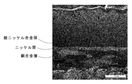
- FIG. 2 is a SIM image of the sample of Example 3 before heating, and it can be seen that the silver-nickel alloy layer is formed on the nickel layer on the base material (copper alloy layer).
- Comparative Example 1 since the film thickness of the silver-nickel alloy layer was as small as 0.2 ⁇ m, the contact resistance value after heating was 2.5 m ⁇ , indicating low heat resistance. In Comparative Example 2, since the nickel content of the silver-nickel alloy layer was as high as 2.5 at %, the contact resistance value after heating was 3.4 m ⁇ , indicating that the heat resistance was low.
- Example 6 to 8 Each sample of Examples 6 to 8 and Comparative Examples 6 to 8 was manufactured by the following method.
- a base material made of a copper alloy plate and having a thickness of 0.3 mm was prepared, and the base material was cleaned (pretreatment step) by degreasing, pickling, etc.
- a part of the surface of the material was subjected to silver strike plating treatment (silver strike plating step) to form a silver strike plating layer.
- the plating time is adjusted so that the film thickness of the silver-nickel alloy layer in Table 3 is obtained, and the silver-nickel alloy plating process is performed (silver-nickel alloy layer forming step).
- the silver-nickel alloy layer was formed directly on the base material.
- the compositions of the silver strike plating bath and the silver nickel alloy plating bath were the same as those used in the first experiment.
- Comparative Example 6 the surface of the base material was subjected to a silver strike plating treatment (Silver strike plating step) in the same manner as in Examples 6 to 8 described above, and then plated so as to have the film thickness of the silver-nickel alloy layer in Table 3. By adjusting the time, silver-nickel alloy plating treatment was performed (silver-nickel alloy layer forming step) to form a silver-nickel alloy layer.
- the silver strike plating treatment was performed on the surface of the base material in the same manner as in Examples 6 to 8 and Comparative Example 6, and then the silver-nickel alloy plating treatment was not performed, and the bright silver plating treatment was performed.
- An alloy layer (AgSb layer) was formed to obtain a sample of Comparative Example 6.
- a plating bath containing antimony (AgCN: 55 g/L, NaCN: 120 g/L, Na 2 CO 3 : 15 g/L, Nisshinbright N (manufactured by Nikoseikai Co., Ltd.): 40 ml/L ), the bath temperature was 25° C., the current density was 1 A/dm 2, and a pure silver plate was used as the anode.
- Comparative Example 8 the surface of the substrate was subjected to a silver strike plating treatment as in Examples 6 to 8 and Comparative Examples 6 and 7, and then the silver-nickel alloy plating treatment was not applied, but the silver plating treatment was applied to obtain a film thickness. A 3 ⁇ m silver layer was formed.
- the silver plating treatment was carried out using a plating bath containing 40 g/L of silver cyanide, 120 g/L of potassium cyanide, 15 g/L of potassium carbonate and 4 ml/L of an additive AgO-56 (manufactured by Atotech Japan) at a bath temperature of 25° C. and an electric current.
- the thickness of the silver-nickel alloy layer formed on the outermost surface of the substrate was 3 to 5 ⁇ m, and the nickel content of the silver-nickel alloy layer was 0. Since it was 0.5 to 1.6 at %, the Vickers hardness before heating was 222 HV or more, and the decrease in hardness after heating was 16 HV or less, and the Vickers hardness after heating was 218 HV or more. It was shown that the property is high.
- the contact resistance value was larger than that in the case where the nickel layer was provided between the base material and the silver-nickel alloy layer in both cases before and after heating, but the maximum was 1.8 m ⁇ . It was shown to be small as follows and high in heat resistance. Further, in Examples 6 to 8, since the silver-nickel alloy layer was formed directly on the base material, peeling did not occur, and the result of the heat-resistant peeling test was "A".
- Comparative Example 6 since the thickness of the silver-nickel alloy layer was as small as 0.3 ⁇ m, the contact resistance value after heating was 4.5 m ⁇ , indicating that the heat resistance was low.
- Comparative Example 7 since the outermost layer is composed of the silver alloy layer (AgSb) containing antimony, the Vickers hardness before heating is as high as 193 HV, but the hardness decrease amount after heating is as large as 54 HV, and The subsequent contact resistance also exceeded 20 m ⁇ , indicating that the wear resistance and heat resistance were low.
- Comparative Example 8 since the outermost layer was composed of the silver layer, the Vickers hardness before and after heating was 110 HV or less, and the hardness reduction amount was as large as 36 HV, indicating that the wear resistance was low. In each of Comparative Examples 6 to 8, each of the silver alloy layer and the silver layer was directly formed on the substrate, so that the results of the heat-resistant peeling test were all “A”.
- Example 9 and 10 in which the nickel layer had a small film thickness, the contact resistance value after heating was higher than that in Example 3 having the same silver-nickel alloy layer film thickness and nickel content. However, sufficient hardness was obtained before and after heating.
Landscapes
- Chemical & Material Sciences (AREA)
- Engineering & Computer Science (AREA)
- Chemical Kinetics & Catalysis (AREA)
- Electrochemistry (AREA)
- Materials Engineering (AREA)
- Metallurgy (AREA)
- Organic Chemistry (AREA)
- Manufacturing & Machinery (AREA)
- Electroplating Methods And Accessories (AREA)
Abstract
Priority Applications (5)
| Application Number | Priority Date | Filing Date | Title |
|---|---|---|---|
| JP2020518564A JP6743998B1 (ja) | 2019-01-24 | 2020-01-22 | コネクタ用端子材及びコネクタ用端子 |
| CN202080006529.8A CN113166965B (zh) | 2019-01-24 | 2020-01-22 | 连接器用端子材及连接器用端子 |
| EP20745808.4A EP3916133A4 (fr) | 2019-01-24 | 2020-01-22 | Matériau de borne de connecteur et terminal de connecteur |
| KR1020217011575A KR20210116422A (ko) | 2019-01-24 | 2020-01-22 | 커넥터용 단자재 및 커넥터용 단자 |
| US17/422,478 US20220069498A1 (en) | 2019-01-24 | 2020-01-24 | Connector terminal material and terminal for connector |
Applications Claiming Priority (2)
| Application Number | Priority Date | Filing Date | Title |
|---|---|---|---|
| JP2019010102 | 2019-01-24 | ||
| JP2019-010102 | 2019-01-24 |
Publications (1)
| Publication Number | Publication Date |
|---|---|
| WO2020153396A1 true WO2020153396A1 (fr) | 2020-07-30 |
Family
ID=71736161
Family Applications (1)
| Application Number | Title | Priority Date | Filing Date |
|---|---|---|---|
| PCT/JP2020/002088 Ceased WO2020153396A1 (fr) | 2019-01-24 | 2020-01-22 | Matériau de borne de connecteur et terminal de connecteur |
Country Status (6)
| Country | Link |
|---|---|
| US (1) | US20220069498A1 (fr) |
| EP (1) | EP3916133A4 (fr) |
| JP (1) | JP6743998B1 (fr) |
| KR (1) | KR20210116422A (fr) |
| CN (1) | CN113166965B (fr) |
| WO (1) | WO2020153396A1 (fr) |
Cited By (1)
| Publication number | Priority date | Publication date | Assignee | Title |
|---|---|---|---|---|
| CN116601339A (zh) * | 2020-12-23 | 2023-08-15 | 同和金属技术有限公司 | 镀Ag材、镀Ag材的制造方法、以及电子部件 |
Families Citing this family (4)
| Publication number | Priority date | Publication date | Assignee | Title |
|---|---|---|---|---|
| KR20220046552A (ko) | 2019-08-09 | 2022-04-14 | 미쓰비시 마테리알 가부시키가이샤 | 커넥터용 단자재 |
| US20240372281A1 (en) * | 2022-03-30 | 2024-11-07 | Furukawa Electric Co., Ltd. | Electrical contact material, and contact, terminal and connector made using this |
| JP7781002B2 (ja) * | 2022-03-30 | 2025-12-05 | 古河電気工業株式会社 | 電気接点材料、ならびにこれを用いた接点、端子およびコネクタ |
| JP7781001B2 (ja) * | 2022-03-30 | 2025-12-05 | 古河電気工業株式会社 | 電気接点材料、ならびにこれを用いた接点、端子およびコネクタ |
Citations (7)
| Publication number | Priority date | Publication date | Assignee | Title |
|---|---|---|---|---|
| JP2001003194A (ja) * | 1999-06-21 | 2001-01-09 | Nippon Mining & Metals Co Ltd | 耐熱,耐食性銀めっき材 |
| JP2008169408A (ja) | 2007-01-09 | 2008-07-24 | Auto Network Gijutsu Kenkyusho:Kk | コネクタ用銀めっき端子 |
| JP2009079250A (ja) * | 2007-09-26 | 2009-04-16 | Dowa Metaltech Kk | 最表層として銀合金層が形成された銅または銅合金部材およびその製造方法 |
| JP2013189680A (ja) * | 2012-03-14 | 2013-09-26 | Dowa Metaltech Kk | 銀めっき材 |
| WO2016157713A1 (fr) * | 2015-03-27 | 2016-10-06 | オリエンタル鍍金株式会社 | Matériau de placage d'argent et son procédé de fabrication |
| JP2018199839A (ja) * | 2017-05-25 | 2018-12-20 | トヨタ自動車株式会社 | 銀めっき液、銀めっき材料及び電気・電子部品、並びに銀めっき材料の製造方法。 |
| JP2019010102A (ja) | 2016-04-14 | 2019-01-24 | 株式会社新菱 | ガス含有基材 |
Family Cites Families (3)
| Publication number | Priority date | Publication date | Assignee | Title |
|---|---|---|---|---|
| AU2685292A (en) * | 1991-09-30 | 1993-05-03 | Olin Corporation | Silver alloys for electrical connector coatings |
| DE10138204B4 (de) * | 2001-08-03 | 2004-04-22 | Ami Doduco Gmbh | Elektrischer Kontakt |
| JP4834022B2 (ja) * | 2007-03-27 | 2011-12-07 | 古河電気工業株式会社 | 可動接点部品用銀被覆材およびその製造方法 |
-
2020
- 2020-01-22 KR KR1020217011575A patent/KR20210116422A/ko not_active Ceased
- 2020-01-22 JP JP2020518564A patent/JP6743998B1/ja active Active
- 2020-01-22 WO PCT/JP2020/002088 patent/WO2020153396A1/fr not_active Ceased
- 2020-01-22 EP EP20745808.4A patent/EP3916133A4/fr not_active Withdrawn
- 2020-01-22 CN CN202080006529.8A patent/CN113166965B/zh not_active Expired - Fee Related
- 2020-01-24 US US17/422,478 patent/US20220069498A1/en not_active Abandoned
Patent Citations (7)
| Publication number | Priority date | Publication date | Assignee | Title |
|---|---|---|---|---|
| JP2001003194A (ja) * | 1999-06-21 | 2001-01-09 | Nippon Mining & Metals Co Ltd | 耐熱,耐食性銀めっき材 |
| JP2008169408A (ja) | 2007-01-09 | 2008-07-24 | Auto Network Gijutsu Kenkyusho:Kk | コネクタ用銀めっき端子 |
| JP2009079250A (ja) * | 2007-09-26 | 2009-04-16 | Dowa Metaltech Kk | 最表層として銀合金層が形成された銅または銅合金部材およびその製造方法 |
| JP2013189680A (ja) * | 2012-03-14 | 2013-09-26 | Dowa Metaltech Kk | 銀めっき材 |
| WO2016157713A1 (fr) * | 2015-03-27 | 2016-10-06 | オリエンタル鍍金株式会社 | Matériau de placage d'argent et son procédé de fabrication |
| JP2019010102A (ja) | 2016-04-14 | 2019-01-24 | 株式会社新菱 | ガス含有基材 |
| JP2018199839A (ja) * | 2017-05-25 | 2018-12-20 | トヨタ自動車株式会社 | 銀めっき液、銀めっき材料及び電気・電子部品、並びに銀めっき材料の製造方法。 |
Non-Patent Citations (1)
| Title |
|---|
| See also references of EP3916133A4 |
Cited By (1)
| Publication number | Priority date | Publication date | Assignee | Title |
|---|---|---|---|---|
| CN116601339A (zh) * | 2020-12-23 | 2023-08-15 | 同和金属技术有限公司 | 镀Ag材、镀Ag材的制造方法、以及电子部件 |
Also Published As
| Publication number | Publication date |
|---|---|
| EP3916133A4 (fr) | 2022-10-05 |
| KR20210116422A (ko) | 2021-09-27 |
| CN113166965B (zh) | 2024-09-27 |
| JP6743998B1 (ja) | 2020-08-19 |
| US20220069498A1 (en) | 2022-03-03 |
| EP3916133A1 (fr) | 2021-12-01 |
| JPWO2020153396A1 (ja) | 2021-02-18 |
| CN113166965A (zh) | 2021-07-23 |
Similar Documents
| Publication | Publication Date | Title |
|---|---|---|
| JP6743998B1 (ja) | コネクタ用端子材及びコネクタ用端子 | |
| JP4834022B2 (ja) | 可動接点部品用銀被覆材およびその製造方法 | |
| JP4834023B2 (ja) | 可動接点部品用銀被覆材およびその製造方法 | |
| JP4402132B2 (ja) | リフローSnめっき材及びそれを用いた電子部品 | |
| JP2003293187A (ja) | めっきを施した銅または銅合金およびその製造方法 | |
| JP7302248B2 (ja) | コネクタ用端子材及びコネクタ用端子 | |
| JP7302364B2 (ja) | コネクタ用端子材及びコネクタ用端子 | |
| CN113166964A (zh) | 防腐蚀端子材及端子和电线末端部结构 | |
| JP2020128575A (ja) | コネクタ用端子材、コネクタ用端子及びコネクタ用端子材の製造方法 | |
| US11901659B2 (en) | Terminal material for connectors | |
| JP7040544B2 (ja) | コネクタ用端子材 | |
| JP7059877B2 (ja) | コネクタ用端子材及びコネクタ用端子 | |
| JP7313600B2 (ja) | コネクタ用端子材及びコネクタ用端子 | |
| JP7494618B2 (ja) | コネクタ用端子材 | |
| CN116134181A (zh) | 连接器用端子材 | |
| JP2020117770A (ja) | コネクタ用端子材及びコネクタ用端子 | |
| JP4570948B2 (ja) | ウィスカー発生を抑制したCu−Zn系合金のSnめっき条及びその製造方法 | |
| JP2020117769A (ja) | コネクタ用端子材及びコネクタ用端子 | |
| WO2021029254A1 (fr) | Matériau de borne pour connecteurs | |
| JP2024102926A (ja) | 皮膜付端子材 | |
| JP2021063250A (ja) | コネクタ用端子材及びその製造方法 | |
| JP2022022071A (ja) | コネクタ用端子材 | |
| JP2020056057A (ja) | コネクタ用端子材、コネクタ用端子及びコネクタ用端子材の製造方法 | |
| JP2021063249A (ja) | コネクタ用端子材 | |
| JP2026075869A (ja) | コネクタ用端子材及びその製造方法 |
Legal Events
| Date | Code | Title | Description |
|---|---|---|---|
| ENP | Entry into the national phase |
Ref document number: 2020518564 Country of ref document: JP Kind code of ref document: A |
|
| 121 | Ep: the epo has been informed by wipo that ep was designated in this application |
Ref document number: 20745808 Country of ref document: EP Kind code of ref document: A1 |
|
| NENP | Non-entry into the national phase |
Ref country code: DE |
|
| ENP | Entry into the national phase |
Ref document number: 2020745808 Country of ref document: EP Effective date: 20210824 |
|
| WWR | Wipo information: refused in national office |
Ref document number: 1020217011575 Country of ref document: KR |
|
| WWW | Wipo information: withdrawn in national office |
Ref document number: 2020745808 Country of ref document: EP |