WO2020161876A1 - Procédé de formation d'un précurseur de motif à ligne mince fonctionnel et procédé de formation d'un motif à ligne mince fonctionnel - Google Patents
Procédé de formation d'un précurseur de motif à ligne mince fonctionnel et procédé de formation d'un motif à ligne mince fonctionnel Download PDFInfo
- Publication number
- WO2020161876A1 WO2020161876A1 PCT/JP2019/004520 JP2019004520W WO2020161876A1 WO 2020161876 A1 WO2020161876 A1 WO 2020161876A1 JP 2019004520 W JP2019004520 W JP 2019004520W WO 2020161876 A1 WO2020161876 A1 WO 2020161876A1
- Authority
- WO
- WIPO (PCT)
- Prior art keywords
- functional
- line pattern
- thin
- pattern precursor
- line
- Prior art date
- Legal status (The legal status is an assumption and is not a legal conclusion. Google has not performed a legal analysis and makes no representation as to the accuracy of the status listed.)
- Ceased
Links
Images





Classifications
-
- B—PERFORMING OPERATIONS; TRANSPORTING
- B05—SPRAYING OR ATOMISING IN GENERAL; APPLYING FLUENT MATERIALS TO SURFACES, IN GENERAL
- B05D—PROCESSES FOR APPLYING FLUENT MATERIALS TO SURFACES, IN GENERAL
- B05D3/00—Pretreatment of surfaces to which liquids or other fluent materials are to be applied; After-treatment of applied coatings, e.g. intermediate treating of an applied coating preparatory to subsequent applications of liquids or other fluent materials
- B05D3/02—Pretreatment of surfaces to which liquids or other fluent materials are to be applied; After-treatment of applied coatings, e.g. intermediate treating of an applied coating preparatory to subsequent applications of liquids or other fluent materials by baking
-
- B—PERFORMING OPERATIONS; TRANSPORTING
- B05—SPRAYING OR ATOMISING IN GENERAL; APPLYING FLUENT MATERIALS TO SURFACES, IN GENERAL
- B05D—PROCESSES FOR APPLYING FLUENT MATERIALS TO SURFACES, IN GENERAL
- B05D5/00—Processes for applying liquids or other fluent materials to surfaces to obtain special surface effects, finishes or structures
-
- H—ELECTRICITY
- H01—ELECTRIC ELEMENTS
- H01B—CABLES; CONDUCTORS; INSULATORS; SELECTION OF MATERIALS FOR THEIR CONDUCTIVE, INSULATING OR DIELECTRIC PROPERTIES
- H01B13/00—Apparatus or processes specially adapted for manufacturing conductors or cables
-
- H—ELECTRICITY
- H01—ELECTRIC ELEMENTS
- H01B—CABLES; CONDUCTORS; INSULATORS; SELECTION OF MATERIALS FOR THEIR CONDUCTIVE, INSULATING OR DIELECTRIC PROPERTIES
- H01B5/00—Non-insulated conductors or conductive bodies characterised by their form
- H01B5/14—Non-insulated conductors or conductive bodies characterised by their form comprising conductive layers or films on insulating-supports
-
- H—ELECTRICITY
- H05—ELECTRIC TECHNIQUES NOT OTHERWISE PROVIDED FOR
- H05K—PRINTED CIRCUITS; CASINGS OR CONSTRUCTIONAL DETAILS OF ELECTRIC APPARATUS; MANUFACTURE OF ASSEMBLAGES OF ELECTRICAL COMPONENTS
- H05K3/00—Apparatus or processes for manufacturing printed circuits
- H05K3/10—Apparatus or processes for manufacturing printed circuits in which conductive material is applied to the insulating support in such a manner as to form the desired conductive pattern
-
- H—ELECTRICITY
- H05—ELECTRIC TECHNIQUES NOT OTHERWISE PROVIDED FOR
- H05K—PRINTED CIRCUITS; CASINGS OR CONSTRUCTIONAL DETAILS OF ELECTRIC APPARATUS; MANUFACTURE OF ASSEMBLAGES OF ELECTRICAL COMPONENTS
- H05K3/00—Apparatus or processes for manufacturing printed circuits
- H05K3/10—Apparatus or processes for manufacturing printed circuits in which conductive material is applied to the insulating support in such a manner as to form the desired conductive pattern
- H05K3/18—Apparatus or processes for manufacturing printed circuits in which conductive material is applied to the insulating support in such a manner as to form the desired conductive pattern using precipitation techniques to apply the conductive material
Definitions
- the present invention relates to a method for forming a functional fine line pattern precursor and a method for forming a functional fine line pattern, and more specifically, to reduce spatial frequency interference and reduce moire (interference fringes) in an electronic device having a functional fine line pattern.
- the present invention relates to a method for forming a functional thin line pattern precursor and a method for forming a functional thin line pattern.
- Patent Document 1 a plurality of geometric figures closed by a linear liquid containing a functional material (conductive material) are formed on a base material, and a coffee stain phenomenon is used when the linear liquid is dried. Then, the functional material is deposited on the inner edge and the outer edge of the linear liquid to form the outer thin lines and the inner thin lines of the functional pattern precursor, and the outer thin lines are crossed and connected to each other, and the inner thin lines are connected to each other. There is disclosed a technique of forming a functional pattern so as not to occur.
- a functional material conductive material
- a closed intersecting region G surrounded by the outer thin lines is formed between the outer thin lines that are intersected with each other.
- a functional pattern is formed by arranging a plurality of geometric figures side by side at a predetermined pitch, an intersection area G is formed at a corner of the geometric figure. It is installed side by side.
- quadrangle figures are arranged in parallel at a predetermined pitch, and the plurality of quadrangle figures are repeated, so that they have a constant spatial frequency.
- the outer thin lines are crossed with each other to form a crossing region G.
- the base material on which the functional pattern is formed is used for electronic devices such as LCD (liquid crystal display) and touch panel sensors.
- LCD liquid crystal display
- touch panel sensors As an example of an electronic device, when a base material having a functional pattern is used for an LCD (liquid crystal display), the base material and the base material having the LCD pixel pattern are combined.
- the LCD pixel pattern overlapping the functional pattern is specifically a dot matrix pattern (pattern) in which LCD pixels are arranged in a grid pattern.
- the LCD pixel pattern which is a dot matrix pattern, also has a specific spatial frequency.
- the frequency is increased along these angles. It will have a component, namely the spatial frequency.
- the LCD pixel pattern has strong spatial frequencies in the 0° and 90° directions.
- the present invention provides a method of forming a functional fine line pattern precursor and a method of forming a functional fine line pattern, which can reduce spatial frequency interference and reduce moire (interference fringes) in an electronic device having a functional fine line pattern.
- the task is to do.
- the first line-shaped liquid containing the functional material on the base material has a closed substantially multi-sided inner edge and an outer edge which are independent from each other by including a region to which the liquid is not applied.
- a polygonal figure is formed, the first line-shaped liquid is dried, and the functional material is deposited along the inner edge and the outer edge to form an inner thin line and an outer thin line containing the functional material.
- 1 form a functional thin line pattern precursor, Then, the second line-shaped liquid containing the functional material is closed on the base material so as to have an inner edge and an outer edge which are independent from each other as an edge portion by including a region to which the liquid is not applied.
- the second functional thin line pattern precursor consisting of In at least one set of the first functional thin line pattern precursor and the second functional thin line pattern precursor, the outer thin line of the first functional thin line pattern precursor and the second functional thin line pattern precursor.
- the first functional thin line pattern precursor and the inner thin line of the second functional thin line pattern precursor are not connected to each other, and the first functionality is connected to the outer thin line of the first functional thin line pattern precursor.
- Forming a fine line pattern precursor and the second functional fine line pattern precursor The maximum curvature portion of the outer thin wire of the first functional thin wire pattern precursor and the maximum curvature portion of the outer thin wire of the second functional thin wire pattern precursor are brought into contact with each other, or overlapped, in the case of overlapping,
- the length in the longitudinal direction of the overlapping region is set to the first functionality. 3.
- the reference line size of the substantially polygonal figure formed by the first line-shaped liquid and the substantially polygonal figure formed by the second line-shaped liquid is set, and the first line-shaped liquid and the second line are set. In the case of forming a substantially polygonal figure smaller than the substantially polygonal figure of the reference size by at least one of the liquids, the amount of liquid applied to the maximum curvature portion is increased.
- At least a part of the inner thin lines of the functional thin line pattern precursor formed by the method for forming a functional thin line pattern precursor according to any one of 1 to 10 above is removed, and is left without being removed.
- a method for forming a functional fine line pattern precursor and a method for forming a functional fine line pattern which can reduce spatial frequency interference and reduce moire (interference fringes) in an electronic device having a functional fine line pattern. can do.
- FIG. 3A is a perspective view illustrating a state in which a functional fine line pattern precursor is formed
- FIG. 3A is a diagram showing a state in which a linear liquid is applied onto a base material
- FIG. Diagram showing the liquid dried It is a figure explaining the flow which conveys a functional material to the edge of liquid
- (a) is a figure showing the case of a line-like liquid which consists of a closed polygonal figure
- (b) is a reference example.
- a diagram showing the case of a liquid which is not a closed substantially polygonal figure The figure which shows the functional thin wire pattern precursor in this embodiment.
- (a) is a figure showing the state where the 1st line-like liquid was given to a substrate.
- (B) is a diagram showing a state in which the first linear liquid on the substrate is dried It is a figure explaining formation of the 2nd functional fine line pattern precursor when a substantially polygonal figure is a substantially quadrangle figure, and (a) is a figure showing the state where the 2nd line-like liquid was given on a substrate.
- (B) is a diagram showing a state in which the second line-shaped liquid on the substrate is dried.
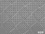
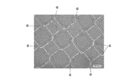
- FIG. 1 Optical micrograph of the state in which the first functional thin line pattern precursor and the second functional thin line pattern precursor are formed on the substrate
- FIG. Diagram illustrating an example of electrolytic plating treatment
- Figure explaining the functional thin line pattern with some thin lines removed The figure explaining an example at the time of forming a functional thin wire pattern on both surfaces of a base material.
- FIG. 4A is a diagram illustrating an application amount of a liquid when forming functional thin line pattern precursors having different sizes, in which (a) is a diagram showing a functional thin line pattern precursor having a standard size, and (b) is a small size.
- FIG. 3A is a diagram for explaining the functional thin line pattern formation in the case where the substantially polygonal shape is a substantially triangular shape
- FIG. 6A shows a state in which the linear liquid is applied so as to form the substantially triangular shape on the base material.
- FIG. 1B is a diagram showing a state in which a functional thin line pattern having a substantially triangular shape is formed.
- FIG. 6A is a diagram illustrating functional thin line pattern formation in the case where a substantially polygonal figure is a substantially hexagonal figure, and (a) is a state in which a linear liquid is applied so as to form a substantially hexagonal figure on a substrate. And (b) is a diagram showing a state in which a functional thin line pattern of a substantially hexagonal figure is formed. The figure explaining the Example of a functional thin line pattern.
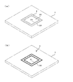
- FIG. 1A and 1B are perspective views illustrating a state in which a functional fine line pattern precursor is formed, where FIG. 1A is a diagram showing a state in which a linear liquid is applied onto a base material, and FIG. 1B is a base material. It is a figure which shows the state which the upper linear liquid dried. A process of forming a functional fine line pattern precursor from a linear liquid will be described with reference to FIG.
- a closed substantially polygonal figure is formed on the base material 1 by the first linear liquid 2.
- the substantially polygonal figure composed of the first line-shaped liquid 2 has an inner edge 21 and an outer edge 22 independent from each other as an edge portion by including the region 20 to which the liquid is not applied inside.
- the inner edge 21 is an inner edge of the closed substantially polygonal figure formed by the first line-shaped liquid 2, and is an edge adjacent to the region 20 to which the liquid is not applied.
- the outer edge 22 is an outer edge of the closed substantially polygonal figure formed by the first linear liquid 2, and is not connected to the inner edge 21.
- the coffee stain phenomenon is used to selectively deposit the functional material along the inner edge 21 and the outer edge 22, which are the edges, as shown in FIG. As shown in b), an inner thin wire 31 is formed at a position corresponding to the inner edge 21, and an outer thin wire 32 is formed at a position corresponding to the outer edge 22.
- the functional thin wire pattern precursor 3 including the inner thin wire 31 containing the functional material and the outer thin wire 32 surrounding the inner thin wire 31 is formed.
- the inner thin wire 31 and the outer thin wire 32 which constitute the functional thin wire pattern precursor 3 are not connected to each other but are independent.
- the inner thin wire 31 and the outer thin wire 32 are sufficiently thinner than the line width (line thickness) of the first linear liquid 2.
- the first linear liquid 2 has one inner edge 21 and one outer edge 22, so that the first functional fine line pattern precursor 3 including the pair of inner fine lines 31 and outer fine lines 32 is formed. Is forming.
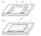
- FIG. 2A and 2B are diagrams for explaining a flow of carrying a functional material to an edge portion of a liquid
- FIG. 2A is a diagram showing a case of a linear liquid having a closed substantially polygonal shape
- FIG. It is a figure which is an example and shows the case of the liquid which is not a closed substantially polygonal figure. The effect of forming the first functional thin line pattern precursor 3 from the first linear liquid 2 will be described with reference to FIG.
- the drying of the first line-shaped liquid 2 applied on the base material 1 is faster at the inner edge 21 and the outer edge 22 than at the central portion, so that the inner edge 21 and the outer portion are first dried.
- Local deposition of functional material occurs along edge 22.
- the accumulated functional material causes the liquid edge to be fixed (fixation of the contact line), and the contraction in the thickness direction of the first line-shaped liquid 2 due to subsequent drying is suppressed.
- the direction of flow is conceptually indicated by an arrow. This flow carries additional functional material to the inner and outer edges 21 and 22 for deposition.
- the inner thin wires 31 and the outer thin wires 32 containing the functional material are formed at the positions corresponding to the inner edge 21 and the outer edge 22, respectively.
- the first line-shaped liquid 2 includes the region 20 to which the liquid is not applied inside, so that the applied amount of the liquid can be reduced and the drying load can be reduced. Thereby, the takt time can be shortened and the production efficiency can be improved.
- the first line-shaped liquid 2 includes the region 20 to which the liquid is not applied inside, the total amount of heat of vaporization accompanying the drying of the liquid becomes relatively small. Therefore, changes in the substrate temperature and non-uniformity due to drying are suppressed, and the above-described liquid flow can be stably formed.
- the first linear liquid 2 can shorten the average moving distance until the functional material reaches the edge by flowing by including the region 20 to which the liquid is not applied inside.
- the coffee stain phenomenon can be stably expressed, and the formation of the inner thin wire 31 and the outer thin wire 32 can be stabilized. ..
- the effect that the inner thin wire 31 and the outer thin wire 32, which are functional thin wires, can be stably formed with a high degree of freedom is obtained.
- Promoting the formation of flows that carry the functional material to the rim is preferable.
- conditions such as the solid content concentration, the contact angle between the liquid and the substrate, the amount of the liquid, the heating temperature of the substrate, the arrangement density of the liquid, or environmental factors such as temperature, humidity, and atmospheric pressure
- the edge of the liquid can be adjusted. Can be fixed at an early stage, and the difference in evaporation amount between the central portion of the liquid and the edge can be increased. This can facilitate the formation of flows that carry the functional material to the edges.
- the application of the first line-shaped liquid 2 onto the base material 1 can be performed by an inkjet method. Specifically, while moving an inkjet head included in a droplet discharge device (not shown) relative to a substrate, ink containing a functional material is discharged from a nozzle of the inkjet head, and the discharged ink droplets are discharged onto the substrate. It is possible to form the line-shaped liquid 2 by coalescing.
- the droplet discharge method of the inkjet head is not particularly limited, and for example, a piezo method or a thermal method can be used.
- the closed substantially polygonal figure can be freely formed in a desired shape by the first line-shaped liquid 2.
- the shapes of the inner edge 21 and the outer edge 22 of the first linear liquid 2 are respectively closed as desired.
- a conductive material is preferably used as the functional material
- a transparent base material is preferably used as the base material.
- the polygonal figure refers to one having a vertex in a state before the liquid is applied on the base material 1, and the substantially polygonal figure means that the polygonal liquid is dried and It means that the vertex of a polygonal figure is changed to the maximum curvature.
- each vertex of the quadrangular figure is formed, and when the drying of the first line-shaped liquid 2 progresses, each vertex has the maximum curvature. And formed into a substantially quadrangular shape.
- the first linear liquid 2 may be applied onto the base material 1 so as to form a substantially quadrangular figure having a maximum curvature portion from the beginning.
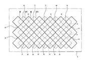
- FIG. 3 is a diagram showing a functional thin line pattern precursor in the present embodiment.
- the maximum curvature portion of the functional thin line pattern precursor will be described by taking the first functional thin line pattern precursor 3 as an example.
- the first linear liquid 2 is dried in the first functional thin line pattern precursor 3, the inner thin line 31 and the outer thin line 32 are formed.
- the liquid of the first line-shaped liquid 2 remains in the position where the inner thin line 31 is formed and the position where the outer thin line 32 is formed.
- the liquid located at each vertex of the quadrangle is pulled in the side direction of the quadrangle extending from each vertex.
- the liquid remaining at each apex is recessed from the state where the corner is formed in the central direction of the quadrangle, and is formed in an arc shape, and becomes the maximum curvature part 311 and the maximum curvature part 321.
- the second functional thin line pattern precursor 5 to be described later is also formed in the same manner as the first functional thin line pattern precursor 3, and the maximum curvature portion 511 and the maximum curvature are obtained by drying the liquid located at each vertex of the quadrangle. It becomes the part 521.
- FIG. 4 is a diagram for explaining the formation of the first functional fine line pattern precursor when the substantially polygonal figure is a substantially quadrangle figure, and (a) shows the first line-shaped liquid applied on the substrate.
- a quadrangle shape is formed as a closed substantially polygonal shape on the base material 1 by the first linear liquid 2 containing a conductive material.
- a plurality of quadrangular first linear liquids 2 are arranged on the base material 1 side by side at a predetermined pitch in the longitudinal direction (vertical direction in the drawing) and width direction (horizontal direction in the drawing) of the base material.
- first line-shaped liquids 2 are shown.
- the first line-shaped liquid 2 applied on the base material 1 has an inner edge 21 and an outer edge 22 independent from each other by including the region 20 to which the liquid is not applied inside.
- the coffee stain phenomenon is caused when the first linear liquid 2 is dried, and the conductive material is selectively deposited along the inner edge 21 and the outer edge 22 of the first linear liquid 2.
- the first functional thin wire pattern precursor 3 including the inner thin wires 31 and the outer thin wires 32 is formed.
- the thin lines 31 and 32 forming the first functional thin line pattern precursor 3 are formed in a substantially rectangular shape.
- Four maximum curvature portions 311 and maximum curvature portions 321 are formed on the thin line 31 and the thin line 32 formed in the substantially quadrangle shape, respectively.
- FIG. 5 is a diagram for explaining the formation of the second functional fine line pattern precursor in the case where the substantially polygonal figure is a substantially quadrangle figure, and (a) shows the second line-shaped liquid applied on the substrate.
- the figure which shows a state (b) is a figure which shows the state in which the 2nd linear liquid on the base material was dried.
- FIG. 6 is an optical micrograph showing a state in which the first functional thin line pattern precursor and the second functional thin line pattern precursor are formed on the substrate.
- a quadrangle figure is formed on the base material 1 as a closed substantially polygonal figure by the second linear liquid 4 containing the conductive material.
- a plurality of second line-shaped liquids 4 each having a quadrangle are arranged in parallel on the base material 1 at a predetermined pitch in the longitudinal direction and the width direction of the base material.
- five second line-shaped liquids 4 are shown.
- the second linear liquid 4 applied on the base material 1 has an inner edge 41 and an outer edge 42 which are independent of each other as an edge by including the region 40 to which the liquid is not applied inside.
- the second linear liquid 4 is formed at the position sandwiched between the four first functional thin line pattern precursors 3.
- the vicinity of each vertex of the quadrangle formed of the second linear liquid 4 is arranged so as to contact the maximum curvature portion 321 of the outer thin wire 32 of the adjacent first functional thin wire pattern precursor 3.
- the vertices of the quadrangle formed of the second linear liquid 4 are arranged in the region between the inner thin line 31 and the outer thin line 32 of the adjacent first functional thin line pattern precursor 3.
- the second functional thin line pattern precursor 5 including the inner thin line 51 and the outer thin line 52 can be formed.
- the thin lines 51 and 52 forming the second functional thin line pattern precursor 5 are formed in a substantially rectangular shape.
- Four maximum curvature portions 511 and maximum curvature portions 521 are formed on the thin line 51 and the thin line 52, which are formed in a substantially quadrangular shape, respectively.
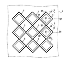
- the first functional thin line pattern precursor 3 and the second functional thin line pattern precursor 5 are provided on the substrate 1 in the longitudinal direction of the substrate. They are formed alternately in the width direction.
- the maximum curvature portion 321 of the outer thin wire 32 of the first functional thin wire pattern precursor 3 and the maximum curvature portion 521 of the outer thin wire 52 of the second functional thin wire pattern precursor 5 are connected to each other, and the first functional thin wire pattern precursor
- the first functional thin wire pattern precursor 3 and the second functional thin wire pattern precursor 5 are formed so that the inner thin wires 31 of the body 3 and the inner thin wires 51 of the second functional thin wire pattern precursor 5 are not connected to each other. doing.
- the inner thin wires 31 and the inner thin wires 51 are not connected to the other inner thin wires 31 and the inner thin wires 51, and are also not connected to the other outer thin wires 32 and the outer thin wires 52.
- the functional thin wire pattern precursor including the first functional thin wire pattern precursor 3 and the second functional thin wire pattern precursor 5 which are connected to each other by the outer thin wires 32 and the outer thin wires 52 on the substrate 1.
- a body pattern is formed.
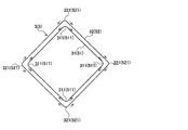
- FIG. 7 is a diagram showing a connection state between the first functional thin line pattern precursor and the second functional thin line pattern precursor in the present embodiment.
- the relationship between the maximum curvature portion 321 of the outer thin wire 32 of the first functional thin wire pattern precursor 3 and the maximum curvature portion 521 of the outer thin wire 52 of the second functional thin wire pattern precursor 5 will be described.
- the functional thin-line pattern precursor comprising the first functional thin-line pattern precursor 3 and the second functional thin-line pattern precursor 5 connected to each other by the outer thin line 32 and the outer thin line 52 on the substrate 1.
- the first functional thin line pattern precursor 3 and the second functional thin line pattern precursor 5 are contacted with the maximum curvature portion 321 of the outer thin wire 32 and the maximum curvature portion 521 of the outer thin wire 52. It is located in.
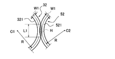
- FIG. 8 is an enlarged view of part A in FIG.
- the outer thin wire 32 and the outer thin wire 52 are each formed with a line width W1.
- the point labeled C1 is the center of curvature of the maximum curvature portion 321
- the point labeled C2 is the center of curvature of the maximum curvature portion 521.
- the maximum curvature portion 321 is formed with a curvature radius of 1/R, where the radius R is a distance R from the curvature center C1 to an imaginary line passing through the center of the outer thin wire 32.
- the maximum curvature part 521 is formed with a curvature radius of 1/R, with the radius of curvature being the distance R from the center of curvature C2 to an imaginary line passing through the center of the outer thin wire 52.
- the maximum curvature portion 321 and the maximum curvature portion 521 are formed with the same curvature, but they may be formed with different curvatures. 7 and 8, for the sake of convenience of description, only a pair of adjacent substantially square-shaped functional thin line pattern precursors (outer thin line 32 and outer thin line 52) are shown, but in FIG. 5(b). As shown, other adjacent substantially square-shaped functional thin line pattern precursors are similarly connected.
- the maximum curvature portion 321 of the outer thin wire 32 and the maximum curvature portion 521 of the outer thin wire 52 are arranged so as to partially overlap each other.
- One overlapping region H is formed in a portion where the maximum curvature portion 321 and the maximum curvature portion 521 overlap.
- the length L1 in the longitudinal direction (vertical direction in FIG. 8) of the overlapping region H is longer than the line width W1 of the outer thin wire 32 and the outer thin wire 52.
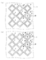
- FIG. 9 is a diagram illustrating an example of electrolytic plating processing. Here, a method for forming a functional thin line pattern composed of the first functional thin line pattern precursor 3 and the second functional thin line pattern precursor 5 formed on the substrate 1 will be described.
- electrolytic plating is performed on the pattern of the functional thin wire pattern precursor consisting of the first functional thin wire pattern precursor 3 and the second functional thin wire pattern precursor 5.
- An example of the electrolytic plating process will be described with reference to FIG.
- the power feeding member 6 is brought into contact with the pattern of the functional thin wire pattern precursor consisting of the first functional thin wire pattern precursor 3 and the second functional thin wire pattern precursor 5 to perform electrolytic plating.
- the outer thin wires 32 of the first functional thin wire pattern precursor 3 and the outer thin wires 52 of the second functional thin wire pattern precursor 5 are connected to each other in the maximum curvature portion 321 and the overlapping region H of the maximum curvature portion 521.
- the energization path including the plurality of outer thin wires 32 and the outer thin wires 52 is formed in a mesh shape.
- the outer thin wires 32 and the outer thin wires 52 in the energizing path are electroplated.
- the inner thin wires 31 and the inner thin wires 51 are not connected to the other inner thin wires 31 and the inner thin wires 51, and are not connected to the other outer thin wires 32 and the outer thin wires 52, and each of them is independent. Since it is formed, the energization path such as the outer thin wire 32 and the outer thin wire 52 described above is not formed.
- the inner thin wire 31 and the inner thin wire 51 that are in direct contact with the power feeding member 6 are present, the inner thin wire 31 and the inner thin wire 51 may be electroplated, but the other inner thin wires 31 and 51 are energized. No, no electrolytic plating is applied.
- the power supply member 6 is not brought into contact with the inner thin wires 31 and the inner thin wires 51, neither of the inner thin wires 31 and the inner thin wires 51 is electrolytically plated.
- the outer thin wires 32 and the outer thin wires 52 can be selectively electroplated.
- selective means that at least the number of outer thin wires 32 and outer thin wires 52 to be electrolytically plated is larger than the number of inner thin wires 31 and inner thin wires 51 to be electrolytically plated.
- FIG. 10 is a diagram for explaining the pattern of the electrolytically plated functional thin wire pattern precursor.
- the film thickness of the outer thin wire 32 and the outer thin wire 52 that are electrolytically plated can be increased compared to the inner thin wire 31 and the inner thin wire 51 that are not electrolytically plated.
- the outer thin wires 32 and the outer thin wires 52 have lower electrical resistance than the inner thin wires 31 and the inner thin wires 51, and the durability is further improved.
- the plating metal used for electrolytic plating is not particularly limited, but it is preferable to use copper or nickel, for example. It is also preferable to stack a plurality of plating layers on the thin wire. In this case, electrolytic plating is performed a plurality of times with different plating metals. For example, preferred is a method of providing a copper plating layer on a fine wire as the first electrolytic plating to improve conductivity, and then providing a nickel plating layer on the copper plating layer as the second electrolytic plating to improve weather resistance. be able to.
- electroless plating instead of electrolytic plating.
- the plating layer can be provided on the thin wire.
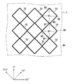
- FIG. 11 is a diagram illustrating a functional thin line pattern in which some thin lines are removed.
- the first functional thin line pattern precursor 3 and the second functional thin line pattern precursor 5 are used as precursors to form a functional thin line pattern.
- the outer thin wires 32 and the outer thin wires 52 are electrolytically plated to increase the film thickness, so that the outer thin wires 32 and the outer thin wires 52 are hard to be removed, and the inner thin wires 31 not electrolytically plated. Also, the inner thin wire 51 can be removed relatively easily.
- the method of removing the fine line is not particularly limited, but it is preferable to use a method of irradiating an energy ray such as a laser beam or a method of chemically etching, for example.
- a method of removing the inner thin wires 31 and the inner thin wires 51 with a plating solution when electrolytically plating the outer thin wires 32 and the outer thin wires 52 can be used.
- the plating liquid a liquid capable of dissolving or decomposing the conductive material forming the thin wire to be removed can be used.
- a fine line pattern precursor 5 is formed.
- a copper plating layer is selectively provided on the outer thin wires 32 and 52 as the first electrolytic plating, and then a nickel plating layer is provided on the copper plating layer as the second electrolytic plating.
- the inner thin wire 31 and the inner thin wire 51 made of silver not subjected to the first electrolytic plating can be dissolved or decomposed and removed by the plating solution of the second electrolytic plating (electrolytic nickel plating).
- a time sufficient for removing the thin wires to be removed preferably the inner thin wires 31 and the inner thin wires 51, preferably 1 minute to 30 minutes, It is also preferable to immerse the material 1 in the plating solution.
- the inner thin wires 31 and the inner thin wires 51 it is possible to adjust the arrangement intervals of the thin wires in the functional thin wire pattern including the outer thin wires 32 and the outer thin wires 52 that remain without being removed with a high degree of freedom. ..
- the adjustment of the arrangement interval by removing a part of the thin line is advantageous especially when the arrangement interval is increased.
- the functional thin wire pattern shown in FIG. 11 has a plurality of thin wires consisting of the outer thin wires 32 and the outer thin wires 52, that is, a plurality of substantially quadrangular thin wires containing a functional material, arranged in a two-dimensional array on the base material 1.
- a plurality of substantially quadrangular thin wires are arranged in parallel at a predetermined pitch in each of the longitudinal direction and the width direction of the base material 1.
- the functional thin line pattern of the present embodiment forms the overlapping region H by overlapping a part of the outer thin line 32 and the outer thin line 52, thereby forming the intersecting regions that are intersected and connected. I don't have it. Therefore, in the functional pattern formed of the substantially quadrangular figure of the maximum curvature portion 321 and the maximum curvature portion 521, the intensity of the spatial frequency of the portion where the overlapping region H of the substantially quadrangle shape is formed can be weakened. As a result, as shown in FIG. 11, the intensity of the spatial frequency in the 0° direction, the 45° direction, the 90° direction, and the 315° direction can be weakened. As a result, in the spatial frequency of the LCD pixel pattern, it is possible to weaken the interference between the spatial frequencies in the 0° direction and the 90° direction, which have a particularly strong intensity, and reduce the occurrence of moire.
- the LCD pixel pattern also has spatial frequencies in the 45° direction and the 315° direction, moire occurs even when the mesh angle (bias angle) of the functional thin line pattern of this embodiment is 45° or 315°. There are cases. In that case, the occurrence of moire can be minimized by adjusting the mesh pitch, which is the fine line interval of the functional fine line pattern, to the LCD pixel pattern.
- the mesh angle (bias angle) can be set to 30° and 60°, or 15° and 75°. Thereby, it is possible to further prevent moire. Particularly, by setting the mesh angle (bias angle) to 30° or 120°, it is possible to minimize the occurrence of moire with the LCD pixel pattern.
- a closed substantially polygonal figure is formed and a part of the fine line is removed to form a functional fine line pattern of the substantially polygonal figure. Therefore, the functional fine line pattern can be stabilized with high flexibility. Can be formed.
- the outer thin wire 32 and the outer thin wire 52 form the overlapping area H.
- the overlapping region H functions as a connecting portion between the outer thin wire 32 and the outer thin wire 52, as shown in FIG.
- the overlapping area H serves as a connecting portion. Since it functions, the electric resistance between the outer thin wire 32 and the outer thin wire 52 can be reduced. As a result, the electrical connection between the outer thin wires 32 and the outer thin wires 52 is ensured, and the electrical resistance of the transparent conductive film can be reduced. Further, since it is possible to preferably prevent the nonuniformity of the electric resistance, it is possible to obtain the effect of improving the stability of the electric resistance.
- the contact length between the outer thin wire 32 and the outer thin wire 52 is also preferable to make the contact length between the outer thin wire 32 and the outer thin wire 52 longer by making the length L1 in the longitudinal direction in the overlapping region H longer than the line width W1 of the outer thin wire 32 and the outer thin wire 52.
- the electrical resistance between the outer thin wire 32 and the outer thin wire 52 can be further reduced, and the stability of the electrical resistance can be further improved.
- the outer thin wire 32 and the outer thin wire 52 are reliably connected. It is possible to prevent the occurrence of short circuit and short circuit.
- FIG. 12 is a diagram illustrating an example of forming a functional thin line pattern on both surfaces of a base material.
- the functional thin wire pattern is formed on one surface (front surface) of the base material 1, and further, the functional thin wire pattern is formed on the other surface (back surface) of the base material 1.
- the functional thin line pattern on each surface is the same as that shown in FIG. 11, in which the inner thin line 31 of the first functional thin line pattern precursor 3 and the inner thin line 51 of the second functional thin line pattern precursor 5 are formed. It is constituted by the outer thin wires 32 of the first functional thin wire pattern precursor 3 and the outer thin wires 52 of the second functional thin wire pattern precursor 5 which are left without being removed by the removal.
- a part of the thin wires constituting the functional thin wire pattern precursor on one surface and/or the other surface is removed to increase the arrangement interval of the thin wires. Is particularly preferable.
- a transparent base material is used as the base material, and a conductive material is used as the functional material to be contained in the functional fine line patterns on both sides, thereby forming the transparent conductive film having the functional fine line patterns on both sides of the transparent base material.
- a transparent base material is used as the base material
- a conductive material is used as the functional material to be contained in the functional fine line patterns on both sides, thereby forming the transparent conductive film having the functional fine line patterns on both sides of the transparent base material. be able to.
- the transparent base material provided with the transparent conductive films on both sides can be suitably used as, for example, a touch panel sensor or the like.
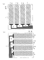
- FIGS. 13A and 13B are diagrams illustrating an example of a touch panel sensor including a transparent conductive film formed of a functional thin line pattern
- FIG. 13A is a diagram showing a state where the base material 1 is viewed from the front surface side
- FIG. FIG. 3 is a diagram showing a state where the base material 1 is viewed from the back surface side.
- a plurality of strip-shaped X electrodes 7 are arranged in parallel on the surface of the transparent base material 1.
- Each of the plurality of X electrodes 7 is formed of a transparent conductive film 8 formed of a functional thin wire pattern including outer thin wires 32 and outer thin wires 52.
- each transparent conductive film 8 the outer thin wires 32 and the outer thin wires 52 adjacent to each other are connected to each other in the overlapping region H.
- the outer thin wires 32 and the outer thin wires 52 forming one transparent conductive film 8 are not connected to the outer thin wires 32 and the outer thin wires 52 forming the other transparent conductive film 8.
- the presence of the outer thin wires 32 and the outer thin wires 52 that are not connected to each other allows the plurality of independent X electrodes 7 that are not electrically connected to each other to be formed on the surface of the base material 1. ..
- Each X electrode 7 is composed of an assembly of a plurality of outer thin wires 32 and outer thin wires 52 electrically connected to each other.
- reference numeral 9 is a lead wire, and each X electrode 7 is connected to a control circuit (not shown) by the lead wire 9.
- a plurality of strip-shaped Y electrodes 10 are arranged side by side on the back surface of the transparent base material 1.
- Each of the plurality of Y electrodes 10 is configured by the transparent conductive film 8 configured by the functional thin wire pattern including the outer thin wires 32 and the outer thin wires 52, similarly to the X electrode 7 described above.
- the strip-shaped Y electrode 10 is formed so that its longitudinal direction intersects the longitudinal direction of the X electrode described above.
- Each Y electrode 10 is connected to a control circuit (not shown) by a lead wiring 9.
- the X electrode 7 and the Y electrode 10 are provided so as to intersect (overlap) with the transparent base material 1 interposed therebetween. At this time, due to the partial removal of the thin wires described above, the arrangement interval of the thin wires in the functional thin wire pattern forming the transparent conductive film forming the X electrode 7 and the Y electrode 10 is increased. As described above, it is possible to alleviate the requirement for high alignment accuracy of the front and back patterns.
- the touch panel sensor having the above configuration can be suitably used as a touch panel sensor of, for example, a capacitance type.
- a capacitance type touch panel an induced current based on a capacitance change generated when a user's finger, a conductor, or the like approaches or contacts the X electrode 7 and the Y electrode 10 during operation, It is possible to detect the position coordinates of a finger, a conductor, or the like.
- the present invention is not limited to this.
- one or more additional functional thin line pattern precursors may be formed.
- the further one or more functional thin line pattern precursors can be formed in one or more times. That is, when a plurality of functional fine line pattern precursors are formed on the substrate, they can be formed appropriately in a plurality of times. Further, for example, when the functional thin line pattern precursors are not connected to each other, it is also preferable to form a plurality of functional thin line pattern precursors once.
- FIG. 14 is a diagram for explaining the applied amount of the liquid in the case of forming functional thin line pattern precursors of different sizes
- (a) is a diagram showing the functional thin line pattern precursor of the standard size
- (b) [Fig. 3] is a diagram showing a small-sized functional fine line pattern precursor.
- the broken line in FIG. 14 indicates the liquid before drying, which is applied to the apex portion of each rectangular figure drawn by the liquid.
- the liquid applied onto the base material 1 After the quadrangle figure is drawn by the liquid applied onto the base material 1, the liquid is dried, so that the vertexes of the quadrangle figure have the maximum curvature portion 311, the maximum curvature portion 321, the maximum curvature portion 511, and the maximum curvature portion 511. It changes to the part 521, and the first functional thin line pattern precursor 3 and the second functional thin line pattern precursor 5 having a substantially rectangular shape are formed.
- the liquid applied to the apex portion of the quadrangle graphic is pulled in each side direction as the liquid dries. As a result, the liquid applied to the apex is drawn toward the center of the quadrangle to form the maximum curvature portion 311, the maximum curvature portion 321, the maximum curvature portion 511, and the maximum curvature portion 521.
- the reference size is set based on the interval between a pair of opposing sides of the quadrangle figure, and the interval is set to 0.7 mm as an example.
- the maximum curvature portions 114 of the outer thin wire 112 can be connected to each other.
- the outer thin wires 112 of the plurality of functional thin wire pattern precursors 11 are reliably connected to each other, and it is possible to prevent a decrease in the stability of electrical resistance such as a short circuit or a short circuit.
- the functional thin line pattern When forming a functional thin line pattern having a size larger than that of the first functional thin line pattern precursor 3 and the second functional thin line pattern precursor 5 which are the functional thin line patterns of the reference size, the functional thin line pattern is formed. It is also preferable to reduce the application amount of the liquid applied to the apex of the quadrangle figure. When the size of the quadrangle figure drawn with the liquid that forms the functional thin line pattern increases, the distance between each side also increases, and the effect of heat of vaporization when the liquid on each side dries is This is because it is less likely to affect the drying of the liquid, and the drying of the entire quadrangle figure becomes faster.
- FIG. 15 is a diagram for explaining the functional thin line pattern in the case where the line width in the maximum curvature portion is made wider than the line width in the portion other than the maximum curvature portion.
- the line width W1 of the first functional thin line pattern precursor 3 and the second functional thin line pattern precursor 5 having a substantially rectangular shape is set to be a uniform width, but instead of this, the maximum curvature portion 321 and the maximum curvature portion 321 are formed.
- the line width in the curved portion 521 may be set to a line width W2 wider than the line width W1.
- FIG. 16 is a diagram showing an overlapping area of outer thin lines in the second embodiment.
- the outer thin lines are configured to form one overlapping region H, but in the second embodiment, the outer thin lines are intersected with each other, but the intersecting regions G are not formed.
- the configurations of the first functional thin line pattern precursor 3 and the second functional thin line pattern precursor 5 in the first embodiment will be described. Note that, in FIG. 16, for convenience of description, only a pair of adjacent functional thin line pattern precursors having substantially rectangular shapes (outer thin lines 32 and outer thin lines 52) are shown, but as shown in FIG. Adjacent, substantially square-shaped, functional thin-line pattern precursors are similarly connected.
- the outer thin wire 32 of the first functional thin wire pattern precursor 3 and the outer thin wire 52 of the second functional thin wire pattern precursor 5 are formed to have a line width W1.
- a maximum curvature portion 321 and a maximum curvature portion 521 are formed on the outer thin wire 32 and the outer thin wire 52, respectively.
- the maximum curvature portion 321 of the outer thin wire 32 and the maximum curvature portion 521 of the outer thin wire 52 are arranged so as to intersect with each other.
- the insides of the maximum curvature portion are formed to contact each other at a contact point P1.
- two overlapping regions H1 and H2 that are in contact with each other at the contact point P1 are formed in the maximum curvature portion 321 and the maximum curvature portion 521.
- an intersection P2 is a point where the outer edge of the outer thin wire 32 and the outer edge of the outer thin wire 52 intersect, and is located at the upper end of the overlapping area H1 in the vertical direction of FIG.
- the intersection P3 is a point where the outer edge of the outer thin wire 32 and the outer edge of the outer thin wire 52 intersect, and is located at the lower end of the overlapping region H2 in the vertical direction of FIG.
- the length L2 is the length in the longitudinal direction from the overlapping region H1 to the overlapping region H2 through the contact point P1. In this embodiment, the length L2 is longer than the line width W1.
- the outer thin wires 32 and the outer thin wires 52 are intersected to form the two overlapping regions H1 and H2, the outer thin wires 32 and the outer thin wires 32 and the outer portions are formed in comparison with the case where the functional thin wire patterns are formed in a grid pattern.
- the area of the region where the thin wire 52 overlaps can be increased, and the electrical connection between the outer thin wire 32 and the outer thin wire 52 can be ensured.
- the electric resistance of the transparent conductive film can be further reduced, and the electric resistance can be stabilized.
- the outer thin line 32 and the outer thin line 52 are intersected to form two overlapping regions H1 and H2, but the intersecting region G shown in FIG. 21 is not formed.
- the functional thin line pattern in the second embodiment does not form the intersecting region G, so that the intensity of the spatial frequency can be weakened in the portion where the two overlapping regions H1 and H2 of the substantially rectangular figure are formed.
- the interference between the spatial frequency of the functional thin line pattern of the present embodiment and the spatial frequency of the LCD pixel pattern in the 0° direction and the 90° direction can be weakened, and the occurrence of moire can be reduced.
- FIG. 17 is a diagram showing a connected state of the functional thin line pattern precursor in the third embodiment.
- the outer thin wires 32 and the outer thin wires 52 do not overlap with each other, but the outer thin wires 32 and the outer thin wires 52 are in contact with each other to form a contact point.
- the configurations of the first functional thin line pattern precursor 3 and the second functional thin line pattern precursor 5 in the first embodiment will be described.
- FIG. 17 shows only a pair of adjacent functional thin line pattern precursors (outer thin line 32 and outer thin line 52) in a substantially rectangular shape, but as shown in FIG. Adjacent substantially rectangular thin wires are similarly connected.
- the functional thin line pattern precursors (outer thin lines 32 and outer thin lines 52) of the substantially rectangular shapes adjacent to each other can be connected at the contact points P, so that the functional thin line pattern precursors of both rectangular shapes can be connected.
- a conductive material is used as, electrical connection can be realized.
- the outer thin wire 32 and the outer thin wire 52 are brought into contact with each other at the maximum curvature portion 321 and the maximum curvature portion 521 to form the contact point P, but the intersection area G shown in FIG. 21 is not formed.
- the functional thin line pattern in the third embodiment does not form the intersecting region G, so that the intensity of the spatial frequency can be weakened in the portion where the contact point P of the substantially quadrangular shape is formed.
- the interference between the spatial frequency of the functional thin line pattern of the present embodiment and the spatial frequency of the LCD pixel pattern in the 0° direction and the 90° direction can be weakened, and the occurrence of moire can be reduced.
- the closed polygonal figure made of the linear liquid is made into a quadrangle figure, and the functional thin line pattern made of the quadrangle figure is formed.
- the closed substantially polygonal figure made of the line-shaped liquid may be a triangle, a pentagon, a hexagon, etc. to form a functional fine line pattern made of a substantially polygonal fine line.
- FIG. 18 is a diagram for explaining the functional thin line pattern formation in the case where the substantially polygonal figure is a substantially triangular figure.
- FIG. 18A is a diagram in which the linear liquid is applied so as to form a substantially triangular figure on the base material.
- FIG. 3B is a diagram showing a state, and FIG. 3B is a diagram showing a state in which a functional thin line pattern having a substantially triangular shape is formed.
- a substantially triangular figure composed of an inner thin line 31 and an outer thin line 32 respectively formed in a triangular shape is formed.
- the first functional thin line pattern precursor 3 can be formed. Adjacent outer thin wires 32 are connected at the maximum curvature portion.
- the outer thin wire 32 that is left without being removed, that is, a substantially triangular shape. It is possible to form a functional thin line pattern composed of a graphic functional thin line pattern precursor.
- FIG. 19 is a diagram for explaining the functional thin line pattern formation in the case where the substantially polygonal figure is a substantially hexagonal figure, and (a) shows a linear liquid so as to form a substantially hexagonal figure on a substrate.
- FIG. 6B is a diagram showing a state in which the functional thin line pattern having a substantially hexagonal shape is formed.
- the closed polygonal shape made of the line-shaped liquid is made into a hexagon, and as shown in FIG. 19A, the hexagonal shape has an inner thin line 31 and an outer thin line 32 formed in hexagonal shapes.
- the first functional thin line pattern precursor 3 can be formed. Adjacent outer thin wires 32 are connected at the maximum curvature portion.
- the outer thin wires 32 By removing the inner thin wires 31 of the functional thin wire pattern precursor composed of the first functional thin wire pattern precursor 3, as shown in FIG. 19(b), the outer thin wires 32 to be left without being removed, that is, approximately six It is possible to form a functional fine line pattern formed by arranging a plurality of functional fine line pattern precursors each having a rectangular shape in a two-dimensional manner.
- the length of one side of the substantially polygonal figure can be freely adjusted.
- the length of one side is preferably 50 ⁇ m or more, 100 ⁇ m or more, 200 ⁇ m or more, 300 ⁇ m or more, 400 ⁇ m or more, 500 ⁇ m or more, and more preferably 1 mm or more.
- stable thin line formation can be realized by applying the line-shaped liquid as a closed substantially polygonal figure. Since stable thin line formation can be realized regardless of the size, the upper limit of the length of one side is not particularly limited and can be appropriately set according to the application. At least one side forming the substantially polygonal figure is preferably within the above range, and more preferably all sides are within the above range.
- the substantially polygonal figure is not limited to the regular polygonal figure, and the lengths of the respective sides and the angles of the interior angles forming the substantially polygonal figure may be different from each other.
- the substantially polygonal figure is configured as a quadrangle figure in which each side is inclined at 45° with respect to the longitudinal direction of the base material, but a combination of 30° and 60° Alternatively, it may be a combination of 15° and 75°.
- a plurality of different substantially polygonal figures may be formed by a plurality of line-shaped liquids provided on the base material.
- a functional thin line pattern that is a combination of a plurality of types of functional thin line pattern precursors each having a different polygonal shape.
- the above-described first line-shaped liquid and second line-shaped liquid preferably have the same shape, but the present invention is not limited to this and may be similar, for example, a combination of a quadrangle graphic and a hexagonal graphic. It may have a different shape.
- the functional material contained in the liquid (ink) for forming the linear liquid is not particularly limited as long as it is a material for imparting a specific function to the base material. Giving a specific function means, for example, imparting conductivity to a base material using a conductive material, or imparting insulating properties to a base material using an insulating material.
- the functional material is preferably a material different from the material forming the surface of the base material to which the functional material is applied.
- Preferred examples of the functional material include a conductive material, an insulating material, a semiconductor material, an optical filter material, and a dielectric material.
- the functional material is preferably a conductive material or a conductive material precursor.
- the conductive material precursor refers to a material that can be converted into a conductive material by performing an appropriate treatment.
- conductive fine particles and conductive polymers can be preferably exemplified.
- the conductive fine particles are not particularly limited, but include Au, Pt, Ag, Cu, Ni, Cr, Rh, Pd, Zn, Co, Mo, Ru, W, Os, Ir, Fe, Mn, Ge, Sn, Ga, Fine particles of In or the like can be preferably exemplified, and among them, the use of metal fine particles such as Au, Ag, and Cu is preferable because fine wires having low electric resistance and corrosion resistance can be formed. From the viewpoint of cost and stability, metal fine particles containing Ag are most preferable.
- the average particle size of these metal fine particles is preferably in the range of 1 to 100 nm, more preferably in the range of 3 to 50 nm.
- the average particle diameter is a volume average particle diameter and can be measured by Zetasizer 1000HS manufactured by Malvern Instruments.
- carbon fine particles as the conductive fine particles.
- the carbon fine particles include graphite fine particles, carbon nanotubes and fullerenes.
- the conductive polymer is not particularly limited, but a ⁇ -conjugated conductive polymer can be preferably mentioned.
- Examples of the ⁇ -conjugated conductive polymer include polythiophenes, polypyrroles, polyindoles, polycarbazoles, polyanilines, polyacetylenes, polyfurans, polyparaphenylenes, polyparaphenylenevinylenes, polyparaphenylene sulfides. Chain-like conductive polymers such as compounds, polyazulenes, polyisothianaphthenes and polythiazyl can be used. Among them, polythiophenes and polyanilines are preferable because high conductivity can be obtained. Most preferably it is polyethylenedioxythiophene.
- the conductive polymer more preferably comprises the above-mentioned ⁇ -conjugated conductive polymer and a polyanion.
- a conductive polymer can be easily produced by chemically oxidatively polymerizing a precursor monomer forming a ⁇ -conjugated conductive polymer in the presence of a suitable oxidant, an oxidation catalyst and a polyanion.
- a conductive polymer (abbreviated as PEDOT/PSS) composed of poly(3,4-ethylenedioxythiophene) and polystyrene sulfonic acid is described in H.264. C. It is marketed as CLEVIOS series by Starck, PEDOT-PASS 483095 and 560598 by Aldrich, and Denatron series by Nagase Chemtex.
- PEDOT/PSS conductive polymer
- polyaniline is commercially available as the ORMECON series from Nissan Kagaku.
- the content of the functional material in the linear liquid 2 applied on the base material 1 is preferably 0.01% by weight or more and 1% by weight or less based on the total amount of the linear liquid 2.
- the content is a value immediately after the line-shaped liquid 2 is applied onto the substrate 1 and before being dried.
- the content of the functional material is in the range of 0.01% by weight or more and 1% by weight or less, fine line formation due to the coffee stain phenomenon is further stabilized.
- the liquid containing the functional material it is possible to use one kind or a combination of two or more kinds such as water and an organic solvent.
- the organic solvent is not particularly limited, but examples thereof include alcohols such as 1,2-hexanediol, 2-methyl-2,4-pentanediol, 1,3-butanediol, 1,4-butanediol and propylene glycol, Examples thereof include ethers such as diethylene glycol monomethyl ether, diethylene glycol monoethyl ether, diethylene glycol monobutyl ether, triethylene glycol monomethyl ether, dipropylene glycol monomethyl ether and dipropylene glycol monoethyl ether.
- the liquid containing the functional material may contain various additives such as a surfactant within a range that does not impair the effects of the present invention.
- a surfactant for example, when the line-shaped liquid 2 is formed on the substrate 1 by using a droplet discharge device, the surface tension is adjusted to stabilize the discharge, etc. Will be possible.
- the surfactant is not particularly limited, but a silicon-based surfactant or the like can be used.
- the silicone-based surfactant is a dimethylpolysiloxane whose side chain or terminal is modified with polyether.
- KF-351A and KF-642 manufactured by Shin-Etsu Chemical Co., Ltd. and BYK347 and BYK348 manufactured by Big Chemie are commercially available.
- the content of the surfactant is preferably 1% by weight or less based on the total amount of the linear liquid 2.
- the substrate to which the liquid containing the functional material is applied is not particularly limited, and examples thereof include glass, plastic (polyethylene terephthalate, polybutylene terephthalate, polyethylene, polypropylene, acrylic, polyester, polyamide, etc.), metal (copper, nickel, Examples thereof include aluminum, iron, etc., or alloys), ceramics, etc. These may be used alone or may be used in a state of being bonded. Among them, plastic is preferable, and polyethylene terephthalate, polyolefins such as polyethylene and polypropylene are preferable.
- the functional material contained in the thin wire is preferably a conductive material.
- a conductive material By using a conductive material, the pattern formed by the aggregate of the fine wires can be suitably used as a transparent conductive film (also referred to as an electrode film or a transparent electrode).
- the use of the substrate with a transparent conductive film is not particularly limited, but it can be used for various devices included in various electronic devices. From the viewpoint of remarkably exerting the effect of the present invention, for example, as a transparent electrode for a display of various systems such as liquid crystal, plasma, organic electroluminescence, and field emission, or a touch panel, a mobile phone, electronic paper, various solar cells, various electros. It can be suitably used as a transparent electrode used in a luminescence light control device or the like. It is particularly preferable to use a substrate with a transparent conductive film as a touch panel sensor for electronic devices such as smartphones and tablet terminals. When used as a touch panel sensor, it is preferable to use the above-described functional thin line pattern as the transparent conductive films (X electrodes and Y electrodes) on both surfaces of the transparent substrate.
- Example 1 Formation of functional fine line pattern (1) ⁇ Ink composition> An ink (liquid containing a functional material) having the following composition was prepared. -Silver nanoparticles (average particle diameter: 20 nm): 0.23% by weight ⁇ Surfactant ("BYK348" manufactured by Big Chemie): 0.05% by weight -Diethylene glycol monobutyl ether (abbreviation: DEGBE) (dispersion medium): 20% by weight ⁇ Water (dispersion medium): Remaining amount
- ⁇ Substrate> As the base material, a PET base material which was surface-treated so that the contact angle of the liquid containing the functional material was 20.3° was prepared. As the surface treatment, "PS-1M” manufactured by Shinko Denki Keiso Co., Ltd. was used for corona discharge treatment.
- Ink is ejected from the inkjet head while moving the inkjet head (“KM1024iLHE-30” (standard droplet volume 30 pL) manufactured by Konica Minolta Co., Ltd.) relative to the substrate, and as shown in FIG.
- a plurality of closed substantially polygonal figures each having an inner edge and an outer edge were formed on the base material by the first line-shaped liquid 2 containing the functional material.
- the substantially polygonal figure is a quadrangle whose sides are inclined at 45° with respect to the longitudinal direction of the substrate.
- the functional material is selectively deposited on the inner edge 21 and the outer edge 22 of the first line-shaped liquid 2, and as shown in FIG.
- a plurality of first functional fine line pattern precursors 3 each including the inner fine line 31 and the outer fine line 32 were formed.
- the inner thin wires 31 and the outer thin wires 32 of each of the obtained first functional thin wire pattern precursors 3 are quadrangles whose sides are inclined at 45° with respect to the longitudinal direction of the base material. In this quadrangle, the interval (mesh pitch) MP between the outer thin wires 32 that form a pair facing each other is 1.43 mm.
- the ink is ejected from the inkjet head while moving the inkjet head relative to the base material, and as shown in FIG. 5A, the second linear liquid 4 containing the functional material is formed on the base material.
- the substantially polygonal figure is a quadrangle figure in which each side is inclined at 45° with respect to the longitudinal direction of the base material.
- the formation position of the second linear liquid 4 is a region where the vertices of the quadrangle of the second linear liquid 4 intersect with the maximum curvature portion 321 of the outer thin wire 32 of the first functional thin wire pattern precursor 3 previously formed. It was set so as to be in contact with each other so as not to form G or overlap with each other.
- the functional material is selectively deposited on the inner edge 41 and the outer edge 42 of the second line-shaped liquid 4, and as shown in FIG.
- a plurality of second functional thin line pattern precursors 5 each including the inner thin line 51 and the outer thin line 52 were formed.
- the inner thin wires 51 and the outer thin wires 52 of each of the obtained second functional thin wire pattern precursors 5 are quadrangles whose sides are inclined at 45° with respect to the longitudinal direction of the base material. In this quadrangle, the interval (mesh pitch) MP between the outer thin wires 32 that form a pair facing each other is 1.43 mm.
- the outer thin wire 32 of the first functional thin wire pattern precursor 3 and the outer thin wire 52 of the second functional thin wire pattern precursor 5 are connected to each other, and the inner thin wire 31 of the first functional thin wire pattern precursor 3 and The inner thin wires 51 of the second functional thin wire pattern precursor 5 are independent of each other and are not connected to each other.
- the drying of the linear liquid is promoted by patterning the linear liquid on the base material placed on the stage heated to 70°C.
- the formed thin wire was subjected to a firing treatment for 10 minutes in an oven at 130°C.
- the outer thin wires 32 and 52 of the functional thin wire pattern precursors 3 and 5 forming the functional thin wire pattern (1) are selectively subjected to copper electrolytic plating.
- a functional fine line pattern (2) similar to the one obtained was obtained. Copper electrolytic plating was performed under the following plating conditions.
- the anode was connected to a copper plate for plating, and the substrate was placed in the plating bath at a position 30 mm away from the copper plate.
- the plating treatment was performed at a constant current of 0.2 A for 1 minute. After the plating was completed, the base material was washed with water and dried.
- ⁇ Plating bath 20 g of copper sulfate pentahydrate, 1.3 g of 1N hydrochloric acid, and 5 g of a gloss-imparting agent (“ST901C” manufactured by Meltex Co.) were prepared with ion-exchanged water so as to be 1000 mL.
- the anode was connected to a nickel plate for plating, and the substrate was placed in the plating bath at a position 30 mm away from the nickel plate.
- the plating treatment was performed at a constant current of 0.2 A for 30 seconds.
- the substrate was left in the plating bath for 10 minutes, washed with water and dried.
- Examples 2 to 10 Comparative Example 1
- Table 1 As shown in Table 1, in Examples 2 to 5, the length L in the longitudinal direction was changed from Example 1 as a parameter.
- Example 6 is different from Example 1 in that the length L in the longitudinal direction and the line width of the maximum curvature portion are changed as parameters.
- the seventh to tenth embodiments are different from the first embodiment in that the length L in the longitudinal direction and the radius of curvature R of the maximum curvature portion are changed as parameters.
- Comparative Example 1 is a functional thin line pattern in which the intersecting area G shown in FIG. 21 is formed.
- the mesh pitch MP in Table 1 described later is the interval between the outer thin lines facing each other and is denoted by the reference symbol MP in FIG. 20, the line width W1 is the line width of the outer thin lines, and the length L in the longitudinal direction is the maximum curvature portion. Is the length of the overlap region, the maximum curvature portion line width is the line width of the outer thin line in the maximum curvature portion, and the maximum curvature portion curvature radius R is the curvature radius in the maximum curvature portion.
- ⁇ Evaluation criteria> ⁇ : Relative standard deviation of resistance is 30% or less ⁇ : Relative standard deviation of resistance is more than 30% and less than 41% ⁇ : Relative standard deviation of resistance is 41% or more
- the transparent base material on which the functional fine line pattern (3) is formed is placed on a 55-inch Full-HD LCD display, visually observed from a position 30 cm away, and the moire is evaluated according to the following evaluation criteria. The visibility was evaluated.
Landscapes
- Engineering & Computer Science (AREA)
- Manufacturing & Machinery (AREA)
- Microelectronics & Electronic Packaging (AREA)
- Manufacturing Of Printed Wiring (AREA)
- Application Of Or Painting With Fluid Materials (AREA)
Abstract
Priority Applications (4)
| Application Number | Priority Date | Filing Date | Title |
|---|---|---|---|
| PCT/JP2019/004520 WO2020161876A1 (fr) | 2019-02-07 | 2019-02-07 | Procédé de formation d'un précurseur de motif à ligne mince fonctionnel et procédé de formation d'un motif à ligne mince fonctionnel |
| CN201980091061.4A CN113365745A (zh) | 2019-02-07 | 2019-02-07 | 功能性细线图案前体的形成方法和功能性细线图案的形成方法 |
| JP2020570303A JP7331870B2 (ja) | 2019-02-07 | 2019-02-07 | 機能性細線パターン前駆体の形成方法及び機能性細線パターンの形成方法 |
| KR1020217024428A KR20210110367A (ko) | 2019-02-07 | 2019-02-07 | 기능성 세선 패턴 전구체의 형성 방법 및 기능성 세선 패턴의 형성 방법 |
Applications Claiming Priority (1)
| Application Number | Priority Date | Filing Date | Title |
|---|---|---|---|
| PCT/JP2019/004520 WO2020161876A1 (fr) | 2019-02-07 | 2019-02-07 | Procédé de formation d'un précurseur de motif à ligne mince fonctionnel et procédé de formation d'un motif à ligne mince fonctionnel |
Publications (1)
| Publication Number | Publication Date |
|---|---|
| WO2020161876A1 true WO2020161876A1 (fr) | 2020-08-13 |
Family
ID=71947773
Family Applications (1)
| Application Number | Title | Priority Date | Filing Date |
|---|---|---|---|
| PCT/JP2019/004520 Ceased WO2020161876A1 (fr) | 2019-02-07 | 2019-02-07 | Procédé de formation d'un précurseur de motif à ligne mince fonctionnel et procédé de formation d'un motif à ligne mince fonctionnel |
Country Status (4)
| Country | Link |
|---|---|
| JP (1) | JP7331870B2 (fr) |
| KR (1) | KR20210110367A (fr) |
| CN (1) | CN113365745A (fr) |
| WO (1) | WO2020161876A1 (fr) |
Citations (8)
| Publication number | Priority date | Publication date | Assignee | Title |
|---|---|---|---|---|
| JP2005152758A (ja) * | 2003-11-25 | 2005-06-16 | Seiko Epson Corp | 膜形成方法、デバイス製造方法および電気光学装置 |
| WO2015083160A2 (fr) * | 2013-12-02 | 2015-06-11 | Clearjet Ltd | Procédé de commande de caractéristiques de mouillabilité |
| JP2017039109A (ja) * | 2015-08-21 | 2017-02-23 | コニカミノルタ株式会社 | 機能性細線パターン前駆体の形成方法、機能性細線パターンの形成方法、透明導電膜の形成方法、デバイスの製造方法及び電子機器の製造方法、並びに、機能性細線パターン、透明導電膜付き基材、デバイス及び電子機器 |
| JP2017162739A (ja) * | 2016-03-10 | 2017-09-14 | コニカミノルタ株式会社 | 透明面状デバイス及び透明面状デバイスの製造方法 |
| WO2018110198A1 (fr) * | 2016-12-16 | 2018-06-21 | コニカミノルタ株式会社 | Procédé de formation d'un film électroconducteur transparent, et liquide de placage pour électrodéposition |
| JP2018098127A (ja) * | 2016-12-16 | 2018-06-21 | コニカミノルタ株式会社 | 透明導電体の製造方法 |
| JP2018094538A (ja) * | 2016-12-16 | 2018-06-21 | コニカミノルタ株式会社 | 細線パターン形成方法及び細線パターン形成装置 |
| JP2018098446A (ja) * | 2016-12-16 | 2018-06-21 | コニカミノルタ株式会社 | タッチパネルセンサー中間体、及びタッチパネルセンサーの製造方法 |
Family Cites Families (1)
| Publication number | Priority date | Publication date | Assignee | Title |
|---|---|---|---|---|
| JPS5988654U (ja) | 1982-12-08 | 1984-06-15 | 三菱重工業株式会社 | 空気調和機 |
-
2019
- 2019-02-07 JP JP2020570303A patent/JP7331870B2/ja active Active
- 2019-02-07 KR KR1020217024428A patent/KR20210110367A/ko not_active Abandoned
- 2019-02-07 CN CN201980091061.4A patent/CN113365745A/zh active Pending
- 2019-02-07 WO PCT/JP2019/004520 patent/WO2020161876A1/fr not_active Ceased
Patent Citations (8)
| Publication number | Priority date | Publication date | Assignee | Title |
|---|---|---|---|---|
| JP2005152758A (ja) * | 2003-11-25 | 2005-06-16 | Seiko Epson Corp | 膜形成方法、デバイス製造方法および電気光学装置 |
| WO2015083160A2 (fr) * | 2013-12-02 | 2015-06-11 | Clearjet Ltd | Procédé de commande de caractéristiques de mouillabilité |
| JP2017039109A (ja) * | 2015-08-21 | 2017-02-23 | コニカミノルタ株式会社 | 機能性細線パターン前駆体の形成方法、機能性細線パターンの形成方法、透明導電膜の形成方法、デバイスの製造方法及び電子機器の製造方法、並びに、機能性細線パターン、透明導電膜付き基材、デバイス及び電子機器 |
| JP2017162739A (ja) * | 2016-03-10 | 2017-09-14 | コニカミノルタ株式会社 | 透明面状デバイス及び透明面状デバイスの製造方法 |
| WO2018110198A1 (fr) * | 2016-12-16 | 2018-06-21 | コニカミノルタ株式会社 | Procédé de formation d'un film électroconducteur transparent, et liquide de placage pour électrodéposition |
| JP2018098127A (ja) * | 2016-12-16 | 2018-06-21 | コニカミノルタ株式会社 | 透明導電体の製造方法 |
| JP2018094538A (ja) * | 2016-12-16 | 2018-06-21 | コニカミノルタ株式会社 | 細線パターン形成方法及び細線パターン形成装置 |
| JP2018098446A (ja) * | 2016-12-16 | 2018-06-21 | コニカミノルタ株式会社 | タッチパネルセンサー中間体、及びタッチパネルセンサーの製造方法 |
Also Published As
| Publication number | Publication date |
|---|---|
| CN113365745A (zh) | 2021-09-07 |
| KR20210110367A (ko) | 2021-09-07 |
| JP7331870B2 (ja) | 2023-08-23 |
| JPWO2020161876A1 (ja) | 2021-12-09 |
Similar Documents
| Publication | Publication Date | Title |
|---|---|---|
| JP6331457B2 (ja) | 塗膜形成方法、透明導電膜付き基材、デバイス及び電子機器 | |
| KR20150043409A (ko) | 도전성 재료를 포함하는 평행선 패턴, 평행선 패턴 형성 방법, 투명 도전막을 구비한 기재, 디바이스 및 전자 기기 | |
| JP6540698B2 (ja) | パターン形成方法、透明導電膜付き基材、デバイス及び電子機器 | |
| JP6413978B2 (ja) | 機能性細線パターン前駆体の形成方法、機能性細線パターンの形成方法、透明導電膜の形成方法、デバイスの製造方法及び電子機器の製造方法、並びに、機能性細線パターン、透明導電膜付き基材、デバイス及び電子機器 | |
| JP6717316B2 (ja) | 機能性細線パターンの形成方法及び機能性細線パターン | |
| JP6439641B2 (ja) | 導電性パターンの形成方法及び導電性パターン | |
| JP6515928B2 (ja) | メッシュ状の機能性パターンの形成方法、メッシュ状の機能性パターン及び機能性基材 | |
| WO2017104652A1 (fr) | Procédé de formation de fil fin conducteur | |
| JP7331870B2 (ja) | 機能性細線パターン前駆体の形成方法及び機能性細線パターンの形成方法 | |
| JP6658800B2 (ja) | 機能性細線パターン、透明導電膜付き基材、デバイス及び電子機器 | |
| KR102003625B1 (ko) | 패턴 형성 방법, 투명 도전막을 구비한 기재, 디바이스 및 전자 기기 | |
| WO2019064595A1 (fr) | Capteur de panneau tactile et procédé de fabrication de capteur de panneau tactile | |
| JP2018098127A (ja) | 透明導電体の製造方法 | |
| JP6988826B2 (ja) | 透明導電膜の形成方法及び電解メッキ用メッキ液 | |
| JP2018098446A (ja) | タッチパネルセンサー中間体、及びタッチパネルセンサーの製造方法 | |
| WO2017110580A1 (fr) | Motif à fil fin fonctionnel et son procédé de fabrication | |
| JP6620758B2 (ja) | 機能性パターン、機能性パターン付き基材及び機能性パターンの形成方法 | |
| JP6451578B2 (ja) | 機能性細線パターンの形成方法 | |
| JP2021008648A (ja) | 導電性パターン薄膜の製造方法 |
Legal Events
| Date | Code | Title | Description |
|---|---|---|---|
| 121 | Ep: the epo has been informed by wipo that ep was designated in this application |
Ref document number: 19914467 Country of ref document: EP Kind code of ref document: A1 |
|
| ENP | Entry into the national phase |
Ref document number: 2020570303 Country of ref document: JP Kind code of ref document: A |
|
| ENP | Entry into the national phase |
Ref document number: 20217024428 Country of ref document: KR Kind code of ref document: A |
|
| NENP | Non-entry into the national phase |
Ref country code: DE |
|
| 122 | Ep: pct application non-entry in european phase |
Ref document number: 19914467 Country of ref document: EP Kind code of ref document: A1 |