WO2020162095A1 - 光電変換素子および撮像装置 - Google Patents
光電変換素子および撮像装置 Download PDFInfo
- Publication number
- WO2020162095A1 WO2020162095A1 PCT/JP2020/000415 JP2020000415W WO2020162095A1 WO 2020162095 A1 WO2020162095 A1 WO 2020162095A1 JP 2020000415 W JP2020000415 W JP 2020000415W WO 2020162095 A1 WO2020162095 A1 WO 2020162095A1
- Authority
- WO
- WIPO (PCT)
- Prior art keywords
- photoelectric conversion
- conversion element
- electrode
- semiconductor material
- organic semiconductor
- Prior art date
- Legal status (The legal status is an assumption and is not a legal conclusion. Google has not performed a legal analysis and makes no representation as to the accuracy of the status listed.)
- Ceased
Links
Images





Classifications
-
- H—ELECTRICITY
- H10—SEMICONDUCTOR DEVICES; ELECTRIC SOLID-STATE DEVICES NOT OTHERWISE PROVIDED FOR
- H10K—ORGANIC ELECTRIC SOLID-STATE DEVICES
- H10K30/00—Organic devices sensitive to infrared radiation, light, electromagnetic radiation of shorter wavelength or corpuscular radiation
- H10K30/30—Organic devices sensitive to infrared radiation, light, electromagnetic radiation of shorter wavelength or corpuscular radiation comprising bulk heterojunctions, e.g. interpenetrating networks of donor and acceptor material domains
- H10K30/353—Organic devices sensitive to infrared radiation, light, electromagnetic radiation of shorter wavelength or corpuscular radiation comprising bulk heterojunctions, e.g. interpenetrating networks of donor and acceptor material domains comprising blocking layers, e.g. exciton blocking layers
-
- H—ELECTRICITY
- H10—SEMICONDUCTOR DEVICES; ELECTRIC SOLID-STATE DEVICES NOT OTHERWISE PROVIDED FOR
- H10K—ORGANIC ELECTRIC SOLID-STATE DEVICES
- H10K39/00—Integrated devices, or assemblies of multiple devices, comprising at least one organic radiation-sensitive element covered by group H10K30/00
- H10K39/30—Devices controlled by radiation
- H10K39/32—Organic image sensors
-
- H—ELECTRICITY
- H10—SEMICONDUCTOR DEVICES; ELECTRIC SOLID-STATE DEVICES NOT OTHERWISE PROVIDED FOR
- H10K—ORGANIC ELECTRIC SOLID-STATE DEVICES
- H10K85/00—Organic materials used in the body or electrodes of devices covered by this subclass
- H10K85/20—Carbon compounds, e.g. carbon nanotubes or fullerenes
- H10K85/211—Fullerenes, e.g. C60
-
- H—ELECTRICITY
- H10—SEMICONDUCTOR DEVICES; ELECTRIC SOLID-STATE DEVICES NOT OTHERWISE PROVIDED FOR
- H10K—ORGANIC ELECTRIC SOLID-STATE DEVICES
- H10K85/00—Organic materials used in the body or electrodes of devices covered by this subclass
- H10K85/10—Organic polymers or oligomers
- H10K85/111—Organic polymers or oligomers comprising aromatic, heteroaromatic, or aryl chains, e.g. polyaniline, polyphenylene or polyphenylene vinylene
- H10K85/113—Heteroaromatic compounds comprising sulfur or selene, e.g. polythiophene
-
- H—ELECTRICITY
- H10—SEMICONDUCTOR DEVICES; ELECTRIC SOLID-STATE DEVICES NOT OTHERWISE PROVIDED FOR
- H10K—ORGANIC ELECTRIC SOLID-STATE DEVICES
- H10K85/00—Organic materials used in the body or electrodes of devices covered by this subclass
- H10K85/20—Carbon compounds, e.g. carbon nanotubes or fullerenes
- H10K85/211—Fullerenes, e.g. C60
- H10K85/215—Fullerenes, e.g. C60 comprising substituents, e.g. PCBM
-
- H—ELECTRICITY
- H10—SEMICONDUCTOR DEVICES; ELECTRIC SOLID-STATE DEVICES NOT OTHERWISE PROVIDED FOR
- H10K—ORGANIC ELECTRIC SOLID-STATE DEVICES
- H10K85/00—Organic materials used in the body or electrodes of devices covered by this subclass
- H10K85/30—Coordination compounds
-
- H—ELECTRICITY
- H10—SEMICONDUCTOR DEVICES; ELECTRIC SOLID-STATE DEVICES NOT OTHERWISE PROVIDED FOR
- H10K—ORGANIC ELECTRIC SOLID-STATE DEVICES
- H10K85/00—Organic materials used in the body or electrodes of devices covered by this subclass
- H10K85/40—Organosilicon compounds, e.g. TIPS pentacene
-
- Y—GENERAL TAGGING OF NEW TECHNOLOGICAL DEVELOPMENTS; GENERAL TAGGING OF CROSS-SECTIONAL TECHNOLOGIES SPANNING OVER SEVERAL SECTIONS OF THE IPC; TECHNICAL SUBJECTS COVERED BY FORMER USPC CROSS-REFERENCE ART COLLECTIONS [XRACs] AND DIGESTS
- Y02—TECHNOLOGIES OR APPLICATIONS FOR MITIGATION OR ADAPTATION AGAINST CLIMATE CHANGE
- Y02E—REDUCTION OF GREENHOUSE GAS [GHG] EMISSIONS, RELATED TO ENERGY GENERATION, TRANSMISSION OR DISTRIBUTION
- Y02E10/00—Energy generation through renewable energy sources
- Y02E10/50—Photovoltaic [PV] energy
- Y02E10/549—Organic PV cells
Definitions
- the present disclosure relates to a photoelectric conversion element and an imaging device.
- Organic semiconductor materials have physical properties and functions that conventional inorganic semiconductor materials such as silicon do not have. Therefore, as disclosed in Non-Patent Document 1, organic semiconductor materials have been actively studied in recent years as semiconductor materials that can realize new semiconductor devices and electronic devices.
- Non-Patent Document 2 a photoelectric conversion element using an organic material thin film can be used as an organic thin film solar cell by extracting charges (that is, carriers) generated by light as energy.
- the photoelectric conversion element is used as an optical sensor such as an image sensor by taking out charges generated by light as an electric signal. You can
- the present disclosure provides a photoelectric conversion element or the like that has spectral sensitivity in the near infrared light region and can reduce dark current.
- a photoelectric conversion element is provided between a first electrode, a second electrode, and the first electrode and the second electrode, and has a donor organic semiconductor material and an acceptor property.
- a photoelectric conversion layer containing an organic semiconductor material, and a hole blocking layer provided between the photoelectric conversion layer and one of the first electrode and the second electrode are provided.
- the ionization potential of the photoelectric conversion layer is 5.3 eV or less.
- the electron affinity of the hole blocking layer is smaller than the electron affinity of the acceptor organic semiconductor material contained in the photoelectric conversion layer. It has spectral sensitivity in the near infrared light region having a wavelength of 650 nm or more and 3000 nm or less.
- An imaging device includes a substrate, a charge detection circuit provided on the substrate, a photoelectric conversion unit provided on the substrate, and an electric charge detection circuit and the photoelectric conversion unit.
- a photoelectric conversion element or the like that has spectral sensitivity in the near infrared light region and can reduce dark current.
- FIG. 1 is a schematic cross-sectional view showing an example of a photoelectric conversion element when there is no hole blocking layer and electron blocking layer.
- FIG. 2 is a schematic cross-sectional view showing an example of the photoelectric conversion element according to the embodiment.
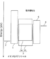
- FIG. 3 is an exemplary energy band diagram in the photoelectric conversion element shown in FIG.
- FIG. 4 is a diagram illustrating an example of a circuit configuration of the image pickup apparatus according to the embodiment.
- FIG. 5 is a schematic cross-sectional view showing an example of a device structure of a pixel of the imaging device according to the embodiment.
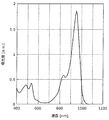
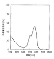
- FIG. 6 is a diagram of an absorption spectrum of the photoelectric conversion layer of Example 1.
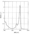
- 7 is a figure of the absorption spectrum of the photoelectric conversion layer of Example 2.
- FIG. 8 is a diagram of an absorption spectrum of the photoelectric conversion layer of Comparative Example 1.
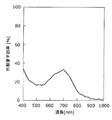
- FIG. 9 is a diagram of a spectral sensitivity spectrum of the photoelectric conversion element of Example 5.
- FIG. 10 is a diagram of a spectral sensitivity spectrum of the photoelectric conversion element of Example 6.
- FIG. 11 is a diagram of a spectral sensitivity spectrum of the photoelectric conversion element of Comparative Example 9.
- the energy level can change when the molecular structure of the organic compound used is changed. Therefore, for example, when an organic semiconductor material is used as a photoelectric conversion material, the absorption wavelength can be controlled, and the spectral sensitivity can be provided even in the near infrared region where silicon (Si) does not have the spectral sensitivity. it can. That is, if an organic semiconductor material is used, it is possible to utilize light in the wavelength region that has not been used for photoelectric conversion in the past, and to improve the efficiency of solar cells and optical sensors in the near infrared light region, etc. Can be realized.
- organic semiconductor materials photoelectric conversion elements, and image pickup elements having a spectral sensitivity in the near infrared light region have been actively studied.
- a photoelectric conversion element using an organic semiconductor material may be referred to as an “organic photoelectric conversion element”.
- sources of dark current generation include charge injection from external electrodes and charge generation in the photoelectric conversion layer.
- a bulk heterostructure photoelectric conversion layer composed of a mixed film of a donor organic semiconductor material and an acceptor organic semiconductor material is used as the photoelectric conversion layer, the donor organic semiconductor material and the cathode are in contact with each other. Since charge injection from the external electrodes is likely to occur, a dark current resulting from charge injection from the external electrodes is likely to occur.
- the ionization potential becomes relatively small with the narrowing of the bandgap to make the absorption wavelength longer, so the charge injection barrier from the cathode The charge injection is promoted due to the decrease in the charge. Therefore, dark current can be suppressed by using a hole blocking layer having a relatively large ionization potential between the photoelectric conversion layer and the cathode.
- the dark current may be generated due to the charge generation in the photoelectric conversion layer as described above.
- the hole blocking layer when the hole blocking layer is used, dark current may be generated due to charge generation at the interface between the photoelectric conversion layer and the hole blocking layer, and the dark current may not be sufficiently suppressed. Charge generation at the interface between the photoelectric conversion layer and the hole blocking layer is affected by the ionization potential and electron affinity of the materials used for the photoelectric conversion layer and the hole blocking layer.
- the inventors of the present invention control the ionization potential of the photoelectric conversion layer and the electron affinity between the photoelectric conversion layer and the hole blocking layer to control the dark current. It has been found that can suppress.
- the present disclosure by controlling the ionization potential of the donor organic semiconductor material, and the electron affinity of the acceptor organic semiconductor material and the hole blocking layer, the spectral sensitivity in the near infrared light region, and Provided is a photoelectric conversion element or the like capable of reducing dark current.
- a photoelectric conversion element is provided between a first electrode, a second electrode, and the first electrode and the second electrode, and has a donor organic semiconductor material and an acceptor property.
- a photoelectric conversion layer containing an organic semiconductor material, and a hole blocking layer provided between one of the first electrode and the second electrode and the photoelectric conversion layer are provided.
- the ionization potential of the photoelectric conversion layer is 5.3 eV or less.
- the electron affinity of the hole blocking layer is smaller than the electron affinity of the acceptor organic semiconductor material contained in the photoelectric conversion layer. It has spectral sensitivity in the near infrared light region having a wavelength of 650 nm or more and 3000 nm or less.
- the “near infrared light region” is a wavelength region where the wavelength of light is 650 nm or more and 3000 nm or less.
- the photoelectric conversion element has “spectral sensitivity” at a certain wavelength means that the external quantum efficiency of the photoelectric conversion element at the wavelength is 1% or more.
- the electron affinity of the hole blocking layer has an acceptor property included in the photoelectric conversion layer even if it has spectral sensitivity in a near infrared light region. Since the electron affinity is smaller than that of the organic semiconductor material, electron excitation at the interface between the photoelectric conversion layer and the hole blocking layer is suppressed. Therefore, it is possible to provide a photoelectric conversion element that has spectral sensitivity in the near infrared light region and can reduce dark current.
- the photoelectric conversion layer may have a maximum absorption wavelength in the near infrared light region.
- the photoelectric conversion layer has the maximum absorption wavelength in the near-infrared light region, and therefore the spectral sensitivity in the near-infrared light region becomes high.
- the photoelectric conversion layer may include, as the acceptor organic semiconductor material, at least one selected from the group consisting of fullerenes and fullerene derivatives.
- the acceptor organic semiconductor material may include a soluble fullerene derivative.
- the acceptor organic semiconductor material is soluble in the solvent, it can be produced in the printing process.
- An imaging device includes a substrate, a charge detection circuit provided in or on the substrate, a photoelectric conversion unit provided on the substrate, and the charge detection circuit and the photoelectric device.
- the imaging device includes the photoelectric conversion element, dark current is reduced while having spectral sensitivity in the near infrared light region. Therefore, the S/N ratio is improved, and good imaging characteristics can be obtained.
- FIG. 1 is a schematic cross-sectional view showing a photoelectric conversion element 10A used for explaining the photoelectric conversion element according to the present embodiment.
- the photoelectric conversion element 10A does not include the hole blocking layer 6 and the electron blocking layer 5 described later, but first, the lower electrode 2 which is the first electrode included in the photoelectric conversion element according to the present embodiment and the second electrode The upper electrode 4, which is the second electrode, and the photoelectric conversion layer 3 will be described.
- the photoelectric conversion element 10A includes an upper electrode 4 which is a first electrode, a lower electrode 2 which is a second electrode, and a photoelectric conversion layer 3 which is provided between the first electrode and the second electrode. Equipped with.
- the photoelectric conversion layer 3 is a mixed film having a bulk hetero structure in which a donor organic semiconductor material and an acceptor organic semiconductor material are mixed.
- the photoelectric conversion element 10A includes a lower electrode 2, an upper electrode 4, and a photoelectric conversion layer 3 provided between the lower electrode 2 and the upper electrode 4.
- the photoelectric conversion element 10A includes a photoelectric conversion layer 3 having absorption in the near infrared light region.
- the photoelectric conversion element 10A is supported by the support substrate 1, for example.
- the support substrate 1 is transparent, and light is incident on the photoelectric conversion element 10A via the support substrate 1.
- the supporting substrate 1 may be a substrate used in a general photoelectric conversion element, and may be, for example, a glass substrate, a quartz substrate, a semiconductor substrate, a plastic substrate, or the like.
- transparent in this specification means that at least a part of light having a wavelength that can be absorbed by the photoelectric conversion layer 3 is transmitted, and it is not essential to transmit light over the entire wavelength range.
- the photoelectric conversion layer 3 of the photoelectric conversion element 10A is made of an organic semiconductor material.
- a coating method such as spin coating or a vacuum evaporation method in which a layer material is vaporized by heating in a vacuum and deposited on a substrate can be used.
- the film can be formed in the atmosphere, N 2 atmosphere or the like, and the film may be formed at a rotation speed of 300 rpm to 3000 rpm.
- the solvent is evaporated after the spin coating to stabilize the film.
- Bake treatment may be performed.
- the baking temperature may be any temperature, but is, for example, 60°C to 250°C.
- a vapor deposition method may be used as a method for producing the photoelectric conversion layer 3 when it is considered that impurities are prevented from being mixed and a multilayer structure for higher functionality is provided with a higher degree of freedom.
- a commercially available device may be used as the vapor deposition device.
- the temperature of the vapor deposition source during vapor deposition may be 100°C to 500°C, or 150°C to 400°C.
- the degree of vacuum during vapor deposition may be 1 ⁇ 10 ⁇ 4 Pa to 1 Pa, or 1 ⁇ 10 ⁇ 3 Pa to 0.1 Pa.
- the photoelectric conversion layer 3 may be produced by a method of adding metal fine particles or the like to the vapor deposition source to increase the vapor deposition rate.
- the blending ratio of the material of the photoelectric conversion layer 3 is indicated by the weight ratio in the coating method and the volume ratio in the vapor deposition method. More specifically, in the coating method, the blending ratio is defined by the weight of each material at the time of solution preparation, and in the vapor deposition method, the blending ratio of each material is monitored while monitoring the deposition layer thickness of each material with a layer thickness meter during deposition. Stipulate.
- the photoelectric conversion layer 3 is composed of a bulk hetero layer which is a mixed film in which a donor organic semiconductor material and an acceptor organic semiconductor material are mixed as a photoelectric conversion material.
- the acceptor organic semiconductor material may include at least one of fullerene and a fullerene derivative.
- the acceptor organic semiconductor material may include soluble fullerene. As a result, the acceptor organic semiconductor material is soluble in the solvent, and thus can be manufactured by a printing process. The details of the donor organic semiconductor material and the acceptor organic semiconductor material will be described later.
- At least one of the upper electrode 4 and the lower electrode 2 is a transparent electrode made of a conductive material that is transparent to light having a response wavelength.
- a bias voltage is applied to the lower electrode 2 and the upper electrode 4 by wiring (not shown).
- the polarity of the bias voltage is determined so that electrons of the charges generated in the photoelectric conversion layer 3 move to the upper electrode 4 and holes move to the lower electrode 2.
- the bias voltage may be set so that holes of the charges generated in the photoelectric conversion layer 3 move to the upper electrode 4 and electrons move to the lower electrode 2.
- the strength of the bias voltage is 1.0 ⁇ 10 3 V/intensity of the electric field generated in the photoelectric conversion element 10A, that is, the value of the applied voltage divided by the distance between the lower electrode 2 and the upper electrode 4. cm to 1.0 ⁇ 10 7 V/cm may be applied, and even within a range of 1.0 ⁇ 10 4 V/cm to 1.0 ⁇ 10 6 V/cm. Good. As described above, by adjusting the magnitude of the bias voltage, it is possible to efficiently move the charges to the upper electrode 4 and take out a signal corresponding to the charges to the outside.
- a transparent conductive oxide (TCO; Transparent Conducting Oxide) having a high transmittance of light in the near infrared light region and a small resistance value may be used.
- TCO transparent Conducting Oxide
- a metal thin film such as gold (Au) can be used as a transparent electrode, but obtain a light transmittance of 90% or more in the near infrared light region. In that case, the resistance value may be extremely increased as compared with the case where the transparent electrode is manufactured so as to obtain the transmittance of 60% to 80%.
- TCO transparent electrode in which TCO is more transparent to near infrared light and has a smaller resistance value than a metal material such as Au.
- TCO is not particularly limited, for example, ITO (Indium Tin Oxide), IZO (Indium Zinc Oxide), AZO (Aluminum-doped Zinc Oxide), FTO (Florine-doped Tin Oxide), SnO 2, TiO 2, ZnO 2 Etc.
- the lower electrode 2 and the upper electrode 4 may be made of TCO, and metal materials such as aluminum (Al) and Au, alone or in combination, depending on the desired transmittance.
- the material of the lower electrode 2 and the upper electrode 4 is not limited to the above-mentioned conductive material having a high transmittance for light in the near infrared light region, and other materials may be used.
- Various methods are used for producing the lower electrode 2 and the upper electrode 4, depending on the materials used.
- ITO an electron beam method, a sputtering method, a resistance heating vapor deposition method, a chemical reaction method such as a sol-gel method, or a method of applying a dispersion of indium tin oxide may be used.
- UV-ozone treatment, plasma treatment or the like may be further performed.
- the photoelectric conversion element 10A photoelectric conversion occurs in the photoelectric conversion layer 3 by the near-infrared light incident via the supporting substrate 1 and the lower electrode 2. Among the generated hole-electron pairs, holes are collected in the lower electrode 2 and electrons are collected in the upper electrode 4. Therefore, for example, by measuring the potential of the lower electrode 2, the near-infrared light that has entered the photoelectric conversion element 10A can be detected.
- the photoelectric conversion element according to the present embodiment includes the hole blocking layer 6 (see FIG. 2) between the photoelectric conversion layer 3 and the electrode of the photoelectric conversion element 10A, and further the photoelectric conversion element 10A performs photoelectric conversion by the hole blocking layer 6.
- An electron blocking layer 5 (see FIG. 2) sandwiching the layer 3 may be provided.
- electrons are injected from the lower electrode 2 to the photoelectric conversion layer 3, and holes are injected from the upper electrode 4 to the photoelectric conversion layer 3. It is possible to suppress the injection. Thereby, the dark current can be suppressed.
- the details of the electron blocking layer 5 and the hole blocking layer 6 will be described later, and thus the description thereof is omitted here.
- FIG. 2 is a schematic sectional view showing the photoelectric conversion element 10B according to the present embodiment.
- the photoelectric conversion element 10B includes a lower electrode 2 which is a first electrode, an upper electrode 4 which is a second electrode, a first electrode and a second electrode.
- the photoelectric conversion layer 3 provided between the electrodes is provided.
- the photoelectric conversion element 10B includes the hole blocking layer 6 provided between the second electrode and the photoelectric conversion layer 3.
- the photoelectric conversion element 10B includes an electron blocking layer 5 arranged between the lower electrode 2 and the photoelectric conversion layer 3, and a hole blocking layer arranged between the upper electrode 4 and the photoelectric conversion layer 3. 6 and 6.
- the method of forming the photoelectric conversion layer 3 and the like are as described above in the description of the photoelectric conversion element 10A, and thus the description thereof is omitted here.
- the photoelectric conversion layer 3 is a bulk hetero layer composed of a mixed film containing a donor organic semiconductor material and an acceptor organic semiconductor material.
- the donor organic semiconductor material and the acceptor organic semiconductor material come into contact with each other, so that electron excitation occurs from the donor organic semiconductor material to the acceptor organic semiconductor material, and even in a dark state. Electric charges may be generated. Therefore, dark current can be suppressed by reducing contact between the donor organic semiconductor material and the acceptor organic semiconductor material. From the viewpoint of charge mobility, when the bulk hetero layer contains a large amount of an acceptor organic semiconductor material such as a fullerene derivative, the device resistance can be suppressed.
- the photoelectric conversion layer 3 has an absorption wavelength in the near infrared light region. Specifically, the absorption edge in the absorption spectrum of the photoelectric conversion layer 3 exists in the near infrared light region. Therefore, the photoelectric conversion element 10B including the photoelectric conversion layer 3 has spectral sensitivity in the near infrared light region. That is, as described above, in the photoelectric conversion element 10B, the external quantum efficiency, which is an index of spectral sensitivity, is 1% or more at any wavelength in the near infrared light region, and may be 10% or more. May be 20% or more. Further, the photoelectric conversion layer 3 may have an absorption maximum wavelength in the near infrared light region. For the photoelectric conversion layer 3, a material having an absorption wavelength in the near infrared light region is used as a donor organic semiconductor material described later.
- the donor organic semiconductor material and the acceptor organic semiconductor material will be specifically exemplified.
- the donor organic semiconductor material is an organic compound having a property of easily donating an electron, which is mainly represented by a hole transporting organic compound. More specifically, the donor organic semiconductor material is an organic compound having a smaller ionization potential when two organic materials are used in contact with each other. Therefore, any organic compound can be used as the donor-type organic semiconductor material as long as it has an absorption wavelength in the near infrared light region and has an electron donating property.
- a metal complex or the like having as a ligand can be used.
- any organic compound having an ionization potential smaller than that of the organic compound used as the acceptor organic semiconductor material may be used as the donor organic semiconductor material.
- the acceptor type organic semiconductor material is an organic compound having a property of easily accepting an electron, which is mainly represented by an electron transporting organic compound. More specifically, the acceptor organic semiconductor material is an organic compound having a larger electron affinity when two organic compounds are used in contact with each other. Therefore, as the acceptor organic compound, any organic compound can be used as long as it is an organic compound having an electron accepting property.
- fullerene, fullerene derivative, condensed aromatic carbocyclic compound naphthalene derivative, anthracene derivative, phenanthrene derivative, tetracene derivative, pyrene derivative, perylene derivative, fluoranthene derivative
- nitrogen atom oxygen atom
- Membered heterocyclic compounds eg pyridine, pyrazine, pyrimidine, pyridazine, triazine, quinoline, quinoxaline, quinazoline, phthalazine, cinnoline, isoquinoline, pteridine, acridine, phenazine, phenanthroline, tetrazole, pyrazole, imidazole, thiazole, oxazole, indazole, benzine)
- Imidazole benzotriazole, benzoxazole, benzothiazole, carbazole, purine, triazolopyrimidine
- a polyarylene compound a fluorene compound, a cyclopentadiene compound, a silyl compound, and a metal complex having a nitrogen-containing heterocyclic compound as a ligand.
- an organic compound having an electron affinity higher than that of the organic compound used as the donor organic semiconductor material may be used as the acceptor organic semiconductor material.
- the acceptor organic semiconductor material may include at least one selected from the group consisting of fullerenes and fullerene derivatives.
- the acceptor organic semiconductor material may contain soluble fullerene. This allows production in a printing process.
- FIG. 3 is a diagram showing an example of a schematic energy band of the photoelectric conversion element 10B having the configuration shown in FIG.
- the ionization potential of the electron blocking layer 5 is larger than the ionization potential of the donor organic semiconductor material 3A contained in the photoelectric conversion layer 3.
- the electron affinity of the hole blocking layer 6 is smaller than the electron affinity of the acceptor organic semiconductor material 3B included in the photoelectric conversion layer 3.
- the electron blocking layer 5 is provided to reduce dark current caused by injection of electrons from the lower electrode 2, and suppresses injection of electrons from the lower electrode 2 into the photoelectric conversion layer 3.
- the material of the electron blocking layer 5 is at least the work function of the lower electrode 2 and the acceptor organic semiconductor material 3B of the photoelectric conversion layer 3. It has a smaller electron affinity than the electron affinity.
- the electron blocking layer 5 has a larger ionization potential and a smaller electron affinity than the donor organic semiconductor material 3A of the photoelectric conversion layer 3.
- the hole blocking layer 6 is provided to reduce dark current due to holes injected from the upper electrode 4.
- the material of the hole blocking layer 6 is at least the work function of the upper electrode 4 and the donor organic semiconductor material of the photoelectric conversion layer 3. It has a larger ionization potential than that of 3A.
- the ionization potential of the hole blocking layer 6 is smaller than the ionization potential of the acceptor semiconductor material 3B of the photoelectric conversion layer 3 in FIG. 3, the ionization potential of the acceptor semiconductor material 3B of the photoelectric conversion layer 3 is not limited to this. It may be higher than the ionization potential.
- the electron affinity of the hole blocking layer 6 larger than the electron affinity of the acceptor organic semiconductor material 3B of the photoelectric conversion layer 3, a larger dark current suppressing effect can be obtained.
- the photoelectric conversion layer 3 has an ionization potential of 5.3 eV or less. As described above, when the ionization potential of the photoelectric conversion layer 3 is relatively small, the dark current suppressing effect of the hole blocking layer 6 according to the present embodiment becomes remarkable. In the case of the photoelectric conversion layer 3 including a mixed film containing a donor organic semiconductor material and an acceptor organic semiconductor material, the donor semiconductor material has a smaller ionization potential than the acceptor semiconductor material. Therefore, the ionization potential of the photoelectric conversion layer 3 is the ionization potential of the donor organic semiconductor material in the photoelectric conversion layer 3.
- the hole blocking layer 6 may have a high transmittance of near-infrared light so as not to interfere with the light absorption of the photoelectric conversion layer 3, and the hole blocking layer 6 also absorbs light in the visible light region as a material of the hole blocking layer 6.
- a material that does not exist may be selected, and the thickness of the hole blocking layer 6 may be reduced.
- the thickness of the hole blocking layer 6 depends on the configuration of the photoelectric conversion layer 3, the thickness of the upper electrode 4, etc., but may be, for example, 2 nm to 50 nm.
- the photoelectric conversion element 10B includes one hole blocking layer 6, but a plurality of hole blocking layers may be provided.
- the electron affinity of the hole blocking layer adjacent to the photoelectric conversion layer may be smaller than the electron affinity of the acceptor organic semiconductor material of the photoelectric conversion layer.
- the material of the lower electrode 2 is selected from the above-mentioned materials in consideration of adhesion with the electron blocking layer 5, electron affinity, ionization potential, stability and the like. The same applies to the upper electrode 4.
- the photoelectric conversion element 10B according to the present embodiment has the light absorption property in the near infrared light region and the dark current is reduced by using the photoelectric conversion material described above. Therefore, according to the present embodiment, it is possible to realize a photoelectric conversion element such as an image pickup element capable of detecting near infrared light.
- the imaging device according to the present embodiment is, for example, a charge readout type imaging device.
- FIG. 4 is a diagram showing an example of a circuit configuration of the image pickup apparatus 100 according to the present embodiment.
- FIG. 5 is a schematic cross-sectional view showing an example of the device structure of the pixel 24 in the imaging device 100 according to this embodiment.
- the imaging device 100 includes a semiconductor substrate 40 that is a substrate, a charge detection circuit 35 provided on the semiconductor substrate 40, a photoelectric conversion unit 10C provided on the semiconductor substrate 40, and a charge detection circuit 35.
- the pixel 24 including the charge storage node 34 electrically connected to the photoelectric conversion unit 10C.
- the photoelectric conversion unit 10C of the pixel 24 includes the photoelectric conversion element 10B.
- the charge storage node 34 stores the charge obtained in the photoelectric conversion unit 10C, and the charge detection circuit 35 detects the charge stored in the charge storage node 34.
- the charge detection circuit 35 provided on the semiconductor substrate 40 may be provided on the semiconductor substrate 40 or may be provided directly in the semiconductor substrate 40.
- the image pickup apparatus 100 includes a plurality of pixels 24 and peripheral circuits.
- the image pickup apparatus 100 is an organic image sensor realized by a one-chip integrated circuit, and has a pixel array including a plurality of pixels 24 arranged two-dimensionally.
- the plurality of pixels 24 are two-dimensionally arranged on the semiconductor substrate 40, that is, arranged in the row direction and the column direction to form a photosensitive area which is a pixel area.
- FIG. 4 shows an example in which the pixels 24 are arranged in a matrix of 2 rows and 2 columns. Note that, in FIG. 4, for convenience of illustration, a circuit (for example, a pixel electrode control circuit) for individually setting the sensitivity of the pixel 24 is omitted.
- the image pickup apparatus 100 may be a line sensor. In that case, the plurality of pixels 24 may be arranged one-dimensionally.
- the row direction and the column direction refer to the directions in which the row and the column extend, respectively. That is, the vertical direction is the column direction and the horizontal direction is the row direction.
- each pixel 24 includes a photoelectric conversion unit 10C and a charge storage node 34 electrically connected to a charge detection circuit 35.
- the charge detection circuit 35 includes an amplification transistor 21, a reset transistor 22, and an address transistor 23.
- the photoelectric conversion unit 10C includes a lower electrode 2 provided as a pixel electrode and an upper electrode 4 provided as a counter electrode.
- the photoelectric conversion unit 10C includes the photoelectric conversion element 10B described above.
- a predetermined bias voltage is applied to the upper electrode 4 via the counter electrode signal line 26.
- the lower electrode 2 is connected to the gate electrode 21G of the amplification transistor 21, and the signal charge collected by the lower electrode 2 is stored in the charge storage node 34 located between the lower electrode 2 and the gate electrode 21G of the amplification transistor 21. To be done.
- the signal charge is a hole in this embodiment, the signal charge may be an electron.
- the signal charge stored in the charge storage node 34 is applied to the gate electrode 21G of the amplification transistor 21 as a voltage according to the amount of the signal charge.
- the amplification transistor 21 amplifies this voltage and is selectively read out as a signal voltage by the address transistor 23.
- the reset transistor 22 has its source/drain electrode connected to the lower electrode 2 and resets the signal charge stored in the charge storage node 34. In other words, the reset transistor 22 resets the potentials of the gate electrode 21G and the lower electrode 2 of the amplification transistor 21.
- the imaging device 100 has a power supply wiring 31, a vertical signal line 27, an address signal line 36, and a reset signal line 37, and these lines are provided. Are connected to the respective pixels 24.
- the power supply wiring 31 is connected to the source/drain electrodes of the amplification transistor 21, and the vertical signal line 27 is connected to the source/drain electrodes of the address transistor 23.
- the address signal line 36 is connected to the gate electrode 23G of the address transistor 23.
- the reset signal line 37 is connected to the gate electrode 22G of the reset transistor 22.
- the peripheral circuit includes a vertical scanning circuit 25, a horizontal signal reading circuit 20, a plurality of column signal processing circuits 29, a plurality of load circuits 28, and a plurality of differential amplifiers 32.
- the vertical scanning circuit 25 is also called a row scanning circuit.
- the horizontal signal reading circuit 20 is also called a column scanning circuit.
- the column signal processing circuit 29 is also called a row signal storage circuit.
- the differential amplifier 32 is also called a feedback amplifier.
- the vertical scanning circuit 25 is connected to the address signal line 36 and the reset signal line 37, selects a plurality of pixels 24 arranged in each row on a row-by-row basis, and reads the signal voltage and resets the potential of the lower electrode 2. To do.
- the horizontal signal read circuit 20 is electrically connected to the plurality of column signal processing circuits 29.
- the column signal processing circuit 29 is electrically connected to the pixels 24 arranged in each column via the vertical signal line 27 corresponding to each column.
- the load circuit 28 is electrically connected to each vertical signal line 27.
- the load circuit 28 and the amplification transistor 21 form a source follower circuit.
- a plurality of differential amplifiers 32 are provided for each column.
- the negative input terminal of the differential amplifier 32 is connected to the corresponding vertical signal line 27.
- the output terminal of the differential amplifier 32 is connected to the pixel 24 via the feedback line 33 corresponding to each column.
- the vertical scanning circuit 25 applies a row selection signal for controlling ON/OFF of the address transistor 23 to the gate electrode 23G of the address transistor 23 by the address signal line 36. As a result, the row to be read is scanned and selected. A signal voltage is read from the pixel 24 in the selected row to the vertical signal line 27. Further, the vertical scanning circuit 25 applies a reset signal for controlling on and off of the reset transistor 22 to the gate electrode 22G of the reset transistor 22 via the reset signal line 37. As a result, the row of the pixels 24 to be reset is selected.
- the vertical signal line 27 transmits the signal voltage read from the pixel 24 selected by the vertical scanning circuit 25 to the column signal processing circuit 29.
- the column signal processing circuit 29 performs noise suppression signal processing represented by correlated double sampling and analog-digital conversion (AD conversion).
- the horizontal signal read circuit 20 sequentially reads signals from a plurality of column signal processing circuits 29 to a horizontal common signal line (not shown).
- the differential amplifier 32 is connected to the drain electrode of the reset transistor 22 via the feedback line 33. Therefore, differential amplifier 32 receives the output value of address transistor 23 at its negative terminal when address transistor 23 and reset transistor 22 are in a conductive state.
- the differential amplifier 32 performs a feedback operation so that the gate potential of the amplification transistor 21 becomes a predetermined feedback voltage. At this time, the output voltage value of the differential amplifier 32 is 0V or a positive voltage near 0V.
- the feedback voltage means the output voltage of the differential amplifier 32.
- the pixel 24 includes a semiconductor substrate 40, a charge detection circuit 35, a photoelectric conversion unit 10C, and a charge storage node 34 (see FIG. 4).
- the semiconductor substrate 40 may be an insulating substrate having a semiconductor layer provided on the surface on the side where the photosensitive region is formed, and is, for example, a p-type silicon substrate.
- the semiconductor substrate 40 has impurity regions (n-type regions here) 21D, 21S, 22D, 22S and 23S, and an element isolation region 41 for electrical isolation between the pixels 24.
- the element isolation region 41 is also provided between the impurity region 21D and the impurity region 22D. As a result, the leak of the signal charge accumulated in the charge accumulation node 34 is suppressed.
- the element isolation region 41 is formed, for example, by performing ion implantation of an acceptor under predetermined implantation conditions.
- amplification transistor 21 includes impurity regions 21S and 21D and a gate electrode 21G.
- the impurity region 21S and the impurity region 21D respectively function as, for example, a source region and a drain region of the amplification transistor 21.
- the channel region of the amplification transistor 21 is formed between the impurity region 21S and the impurity region 21D.
- the address transistor 23 includes impurity regions 23S and 21S and a gate electrode 23G connected to the address signal line 36.
- the amplification transistor 21 and the address transistor 23 are electrically connected to each other by sharing the impurity region 21S.
- the impurity region 23S functions as, for example, a source region of the address transistor 23.
- Impurity region 23S has a connection with vertical signal line 27 shown in FIG.
- the reset transistor 22 includes impurity regions 22D and 22S and a gate electrode 22G connected to the reset signal line 37.
- the impurity region 22S functions as, for example, the source region of the reset transistor 22.
- Impurity region 22S has a connection with reset signal line 37 shown in FIG.
- An interlayer insulating layer 50 is laminated on the semiconductor substrate 40 so as to cover the amplification transistor 21, the address transistor 23, and the reset transistor 22.
- a wiring layer (not shown) may be arranged in the interlayer insulating layer 50.
- the wiring layer is typically formed of a metal such as copper and may include, for example, a wiring such as the vertical signal line 27 described above as a part thereof.
- the number of insulating layers in the interlayer insulating layer 50 and the number of layers included in the wiring layers arranged in the interlayer insulating layer 50 can be set arbitrarily.
- a contact plug 54 connected to the impurity region 22D of the reset transistor 22 a contact plug 53 connected to the gate electrode 21G of the amplification transistor 21, a contact plug 51 connected to the lower electrode 2, and Wirings 52 connecting the contact plugs 51, 54, and 53 are arranged.
- the impurity region 22D of the reset transistor 22 is electrically connected to the gate electrode 21G of the amplification transistor 21.
- the charge detection circuit 35 detects the signal charge captured by the lower electrode 2 and outputs a signal voltage.
- the charge detection circuit 35 includes an amplification transistor 21, a reset transistor 22, and an address transistor 23, and is formed on the semiconductor substrate 40.
- the amplification transistor 21 is formed in the semiconductor substrate 40 and functions as a drain electrode and a source electrode, respectively, and an impurity region 21D and an impurity region 21S, a gate insulating layer 21X formed on the semiconductor substrate 40, and a gate insulating layer 21X. And a gate electrode 21G formed in.
- the reset transistor 22 is formed in the semiconductor substrate 40 and functions as a drain electrode and a source electrode, respectively, an impurity region 22D and an impurity region 22S, a gate insulating layer 22X formed on the semiconductor substrate 40, and a gate insulating layer 22X. And a gate electrode 22G formed in.
- the address transistor 23 is formed in the semiconductor substrate 40 and functions as a drain electrode and a source electrode, respectively, and has impurity regions 21S and 23S, a gate insulating layer 23X formed on the semiconductor substrate 40, and a gate insulating layer 23X. And the gate electrode 23G is formed.
- the impurity region 21S is shared by the amplification transistor 21 and the address transistor 23, whereby the amplification transistor 21 and the address transistor 23 are connected in series.
- the above-described photoelectric conversion unit 10C is arranged on the interlayer insulating layer 50.
- the plurality of pixels 24 forming the pixel array are formed on the semiconductor substrate 40.
- the plurality of pixels 24 arranged two-dimensionally on the semiconductor substrate 40 form a photosensitive area.
- the distance (pixel pitch) between two adjacent pixels 24 may be, for example, about 2 ⁇ m.
- the photoelectric conversion unit 10C has the structure of the photoelectric conversion element 10B described above.
- a color filter 60 is formed above the photoelectric conversion unit 10C, and a microlens 61 is formed above the color filter 60.
- the color filter 60 is formed as an on-chip color filter by patterning, for example, and a photosensitive resin in which a dye or a pigment is dispersed is used.
- the microlens 61 is formed, for example, as an on-chip microlens, and an ultraviolet photosensitive material or the like is used.
- the imaging device 100 can be manufactured using a general semiconductor manufacturing process.
- a silicon substrate is used as the semiconductor substrate 40, it can be manufactured by utilizing various silicon semiconductor processes.
- the photoelectric conversion element according to the present disclosure will be specifically described with reference to Examples, but the present disclosure is not limited to the following Examples. Specifically, various samples according to the embodiments of the present disclosure were prepared, and the absorption edge, the ionization potential, the electron affinity, and the dark current were measured.
- a phenyl group may be represented by Ph
- C 4 H 9 may be represented by Bu
- C 6 H 13 may be represented by Hex
- C 48 H 26 N 8 may be represented by Nc.
- Example 1 ⁇ Sample preparation> A 0.7 mm-thick quartz glass (quartz substrate) is used as a supporting substrate, and on the photoelectric conversion layer, PCPDTBT (manufactured by Merck Sigma-Aldrich, structural formula (1) below) of a donor organic semiconductor material is provided, A mixed solution of phenyl C 61 butyric acid methyl ester (PCBM: ([6,6]-Phenyl-C61-Butyric Acid Metal Ester, Frontier Carbon Co., Ltd.), the following structural formula (2)) as an acceptor organic semiconductor material is spun. It was applied by a coating method to form a mixed film. The weight ratio of PCPDTBT and PCBM in the mixed solution is 1:3, and the solvent is chlorobenzene. The concentration of PCPDTBT and PCBM in the mixed solution is 30 mg/ml. The thickness of the mixed film obtained at this time was about 150 nm.
- PCPDTBT manufactured by Merck Sigma-Aldrich, structural formula (1) below
- PCBM pheny
- the absorption spectrum of the photoelectric conversion layer formed on the quartz substrate was measured with a spectrophotometer (U4100, manufactured by Hitachi High-Technology). The obtained absorption spectrum is shown in FIG. In the photoelectric conversion layer of Example 1, an absorption maximum peak was observed near 715 nm. The absorption edge was estimated from the rising position on the long wavelength side of the absorption spectrum. In the present example, the intersection of the tangent line extended from the point where the rising slope of the absorption spectrum on the long wavelength side is maximized and the wavelength axis (absorbance is zero) was defined as the absorption edge. Table 1 shows the obtained measurement results.
- ⁇ Measurement of ionization potential> The same photoelectric conversion layer as in ⁇ Sample preparation> was formed on the ITO substrate, and the ionization potential was measured.
- An atmospheric photoelectron spectrometer AC-3, manufactured by Riken Keiki Co., Ltd. was used to measure the ionization potential.
- the measurement of the ionization potential is detected as the number of photoelectrons when the energy of ultraviolet irradiation is changed. Therefore, the energy position at which photoelectrons are detected can be set as the ionization potential. Table 1 shows the obtained measurement results.
- Example 2 As donor organic semiconductor material, represented by the following structural formula (3) instead of PCPDTBT (OBu) 8 Si (OPOPh -3,5bisCF 3) 2 Nc ( Japanese Patent Application No. 2018 is a patent application unpublished by the applicant (Synthesis based on -215957) was used, and the same operations as in Example 1 were performed to prepare a sample, measure the absorption edge, and measure the ionization potential. The thickness of the mixed film obtained at this time was about 230 nm.
- Comparative Example 1 As the donor organic semiconductor material, the same operation as in Example 1 was performed except that Si(OSiHex 3 ) 2 Nc (manufactured by Merck Sigma-Aldrich) represented by the following structural formula (4) was used instead of PCPDTBT, Sample preparation, absorption edge measurement, and ionization potential measurement were performed. The thickness of the mixed film obtained at this time was about 180 nm.
- Si(OSiHex 3 ) 2 Nc manufactured by Merck Sigma-Aldrich
- the photoelectric conversion layers of Example 1, Example 2 and Comparative Example 1 all have spectral sensitivity in the near infrared light region because their absorption edges are in the near infrared light region. I was able to confirm that. Moreover, the ionization potentials of the photoelectric conversion layers of Example 1, Example 2, and Comparative Example 1 were 5.1 eV, 5.3 eV, and 5.4 eV, respectively.
- Example 3 Example 4, Comparative Example 2, Comparative Example 3, and Comparative Example 4 will be shown, and regarding the ionization potential and electron affinity of the acceptor organic semiconductor material of the photoelectric conversion layer and the hole blocking layer according to the present disclosure, This will be specifically described.
- the ionization potential and electron affinity of the acceptor organic semiconductor material and the hole blocking layer were measured with a single film.
- Example 3 ⁇ Sample preparation method> A 0.7 mm thick quartz glass (quartz substrate) is used as a supporting substrate, and phenyl C 61 butyric acid methyl ester (PCBM:([6,6]-Phenyl-) is used as an acceptor organic semiconductor material for the photoelectric conversion layer.
- PCBM phenyl C 61 butyric acid methyl ester
- the thickness of the organic material thin film obtained at this time was about 30 nm.
- ⁇ Measurement of ionization potential> The same organic material thin film as in ⁇ Sample preparation> was formed on the ITO substrate, and the ionization potential was measured. The ionization potential was measured in the same manner as in Example 1 except that the above organic material thin film was used. The results of the obtained ionization potential are shown in Table 2.
- the optical band gap was calculated as the difference between the ionization potential and the electron affinity from the result of the absorption edge obtained in the above ⁇ Measurement of absorption edge>.
- the electron affinity was estimated by subtracting the result of the ionization potential obtained in ⁇ Measurement of the ionization potential> and the optical band gap. The obtained electron affinity results are shown in Table 2.
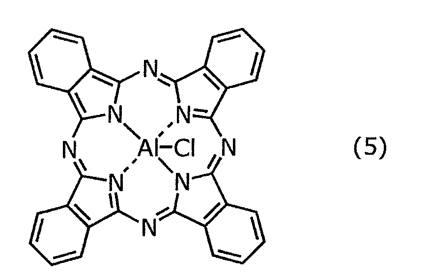
- Example 4 The same as Example 3 except that ClAlPc (manufactured by Merck Sigma-Aldrich Co.) represented by the following structural formula (5), which is a material of the hole blocking layer, was formed by a vacuum deposition method instead of PCBM. Then, the sample preparation, absorption edge measurement, ionization potential measurement, and electron affinity measurement were performed. In addition, the thickness of the organic material thin film obtained at this time was about 30 nm.
- ClAlPc manufactured by Merck Sigma-Aldrich Co.
- Table 2 shows the results of the obtained ionization potential and electron affinity.
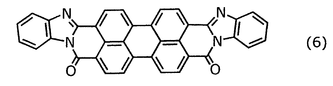
- Example 2 instead of using ClAlPc as the material, the same operation as in Example 4 was performed except that PTCBI (manufactured by Tokyo Kasei) represented by the following structural formula (6), which is the material of the hole blocking layer, was used to prepare a sample. , The absorption edge, the ionization potential, and the electron affinity were measured. In addition, the thickness of the organic material thin film obtained at this time was about 30 nm.
- PTCBI manufactured by Tokyo Kasei
- structural formula (6) which is the material of the hole blocking layer
- Table 2 shows the results of the obtained ionization potential and electron affinity.
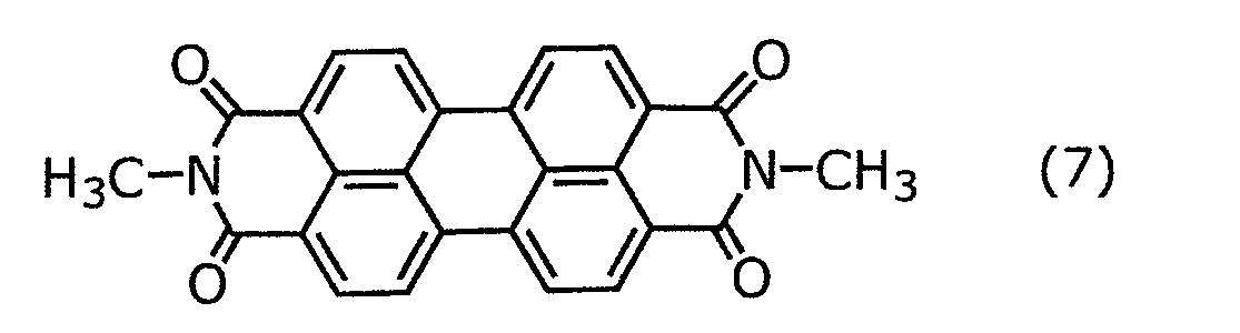
- Example 3 A sample was prepared in the same manner as in Example 4 except that PTCDI (manufactured by Tokyo Kasei) represented by the following structural formula (7), which is a material for the hole blocking layer, was used instead of ClAlPc as a material. , The absorption edge, the ionization potential, and the electron affinity were measured. The thickness of the organic material thin film obtained at this time was about 25 nm.
- PTCDI manufactured by Tokyo Kasei
- structural formula (7) which is a material for the hole blocking layer
- Table 2 shows the results of the obtained ionization potential and electron affinity.
- Example 4 The same operation as in Example 4 was performed except that C60 (fullerene, manufactured by Frontier Carbon Co.) represented by the following structural formula (8), which is a material for the hole blocking layer, was used instead of using ClAlPc as the material. , Sample preparation, absorption edge measurement, ionization potential measurement, and electron affinity measurement were performed. The thickness of the organic material thin film obtained at this time was about 50 nm.
- C60 fulllerene, manufactured by Frontier Carbon Co.
- ClAlPc ClAlPc
- Table 2 shows the results of the obtained ionization potential and electron affinity.
- the hole blocking layer made of ClAlPc of Example 4 has a smaller electron affinity than the acceptor-type organic semiconductor material in the photoelectric conversion layer made of PCBM of Example 3, and the positive holes of Comparative Examples 2 to 4 are positive. It was confirmed that the hole blocking layer had a higher electron affinity than PCBM.
- Example 5 Near infrared photoelectric conversion element
- Example 6 Comparative Examples 5 to 12 will be shown to more specifically describe the near-infrared photoelectric conversion element according to the present disclosure.
- a photoelectric conversion element sample was produced by the following procedure. All sample preparations were performed under nitrogen atmosphere. First, a glass substrate having a thickness of 0.7 mm and having an ITO film having a thickness of 150 nm as a lower electrode on one main surface was prepared. On the lower electrode, a VNPB (N4, N4'-di(Naphthalen-1-yl)-N4, N4'-bis(4-vinylphenyl)biphenyl-4,4'-diamine, manufactured by LUMTEC) solution (solvent: o -Xylene, 10 mg/ml) was applied by a spin coating method to form an electron blocking layer.
- VNPB N4, N4'-di(Naphthalen-1-yl)-N4, N4'-bis(4-vinylphenyl)biphenyl-4,4'-diamine, manufactured by LUMTEC
- the substrate after film formation was crosslinked and insolubilized by heating at 200°C for 50 minutes using a hot plate. Thereafter, as the photoelectric conversion layer, a mixed solution of PCPDTBT and PCBM (weight ratio 1:3, solvent: chlorobenzene, 30 mg/ml) was applied by spin coating as in Example 1 to form a mixed film. did. The thickness of the mixed film obtained at this time was about 150 nm.
- ClAlPc which is the same material as in Example 4, was formed as a hole blocking layer with a thickness of 30 nm by a vacuum evaporation method through a metal shadow mask.
- an Al electrode having a thickness of 80 nm was formed as an upper electrode on the formed hole blocking layer to obtain a photoelectric conversion element.
- the Al electrode was formed into a film with a vacuum degree of 5.0 ⁇ 10 ⁇ 4 Pa or less and a deposition rate of 1 ⁇ /s.
- Example 5 Since the photoelectric conversion layer in Example 5 is made of the same material as the photoelectric conversion layer in Example 1, Table 3 shows the results of the ionization potential measured in Example 1. Further, since the hole blocking layer in Example 5 is formed of the same material as the hole blocking layer in Example 4, the results of electron affinity measured in Example 4 are shown in Table 3.
- a photoelectric conversion element was manufactured by the same method as described above except that the hole blocking layer was not formed in the above ⁇ Production of photoelectric conversion element> to obtain a comparative photoelectric conversion element.
- Relative dark current dark current value of photoelectric conversion element / dark current value of photoelectric conversion element for comparison
- Table 3 shows the results of the obtained relative dark current.
- the spectral sensitivity of the obtained photoelectric conversion element was measured. Specifically, a photoelectric conversion element is introduced into a measuring jig that can be sealed in a glove box under a nitrogen atmosphere, and a long wavelength compatible spectral sensitivity measuring device (CEP-25RR manufactured by Spectrometer Co., Ltd.) is used. The spectral sensitivity was measured under voltage conditions. The result of the obtained spectral sensitivity measurement is shown in FIG. Since the rising edge of the spectral sensitivity spectrum on the long wavelength side is near 900 nm, the photoelectric conversion element in Example 5 has spectral sensitivity in the near infrared light region. Table 3 shows the obtained external quantum efficiency at the maximum peak wavelength in the near infrared light region.
- Example 5 As the hole blocking layer, the same operation as in Example 5 was performed except that PTCBI, which was the same material as in Comparative Example 2, was used instead of ClAlPc, to produce a photoelectric conversion element, a comparative photoelectric conversion element, The dark current and the spectral sensitivity were measured.
- Table 3 shows the ionization potential of the obtained photoelectric conversion layer, the electron affinity of the hole blocking layer, the relative dark current, and the external quantum efficiency.
- Example 6 As the hole blocking layer, the same operation as in Example 5 was performed except that PTCDI, which was the same material as in Comparative Example 3, was used instead of ClAlPc, to produce a photoelectric conversion element, a comparative photoelectric conversion element, The dark current and the spectral sensitivity were measured. Table 3 shows the ionization potential of the obtained photoelectric conversion layer, the electron affinity of the hole blocking layer, the relative dark current, and the external quantum efficiency.
- Comparative Example 7 As the hole blocking layer, the same operation as in Example 5 was performed except that C60, which was the same material as in Comparative Example 4, was used in place of ClAlPc, to produce a photoelectric conversion element, a comparative photoelectric conversion element, The dark current and the spectral sensitivity were measured. Table 3 shows the ionization potential of the obtained photoelectric conversion layer, the electron affinity of the hole blocking layer, the relative dark current, and the external quantum efficiency.
- Example 6 As a photoelectric conversion layer, in place of the mixed solution of PCPDTBT and PCBM, except for using a mixed solution of the same material as in Example 2 (OBu) 8 Si (OPOPh -3,5bisCF 3) 2 Nc and PCBM Then, the same operation as in Example 5 was performed to prepare a photoelectric conversion element, a comparative photoelectric conversion element, a dark current, and a spectral sensitivity.
- Table 3 shows the ionization potential of the obtained photoelectric conversion layer, the electron affinity of the hole blocking layer, the relative dark current, and the external quantum efficiency. The results of the obtained spectral sensitivity measurement are shown in FIG. Since the rising edge of the spectral sensitivity spectrum on the long wavelength side is around 1000 nm, the photoelectric conversion element in Example 6 has spectral sensitivity in the near infrared light region.
- Comparative Example 8 As the hole blocking layer, the same operation as in Example 6 was performed except that C60, which was the same material as in Comparative Example 4, was used in place of ClAlPc, to produce a photoelectric conversion element, a comparative photoelectric conversion element, The dark current and the spectral sensitivity were measured. Table 3 shows the ionization potential of the obtained photoelectric conversion layer, the electron affinity of the hole blocking layer, the relative dark current, and the external quantum efficiency.
- Comparative Example 9 The same operation as in Example 5 except that a mixed solution of Si(OSiHex 3 ) 2 Nc, which is the same material as Comparative Example 1, and PCBM was used as the photoelectric conversion layer instead of the mixed solution of PCPDTBT and PCBM. Then, a photoelectric conversion element, a comparative photoelectric conversion element, a dark current and a spectral sensitivity were measured. Table 3 shows the ionization potential of the obtained photoelectric conversion layer, the electron affinity of the hole blocking layer, the relative dark current, and the external quantum efficiency. The result of the obtained spectral sensitivity measurement is shown in FIG. Since the rise on the long wavelength side of the spectral sensitivity spectrum is around 850 nm, the photoelectric conversion element in Comparative Example 9 has spectral sensitivity in the near infrared light region.
- Comparative Example 10 As the hole blocking layer, the same operation as in Comparative Example 9 was performed except that PTCBI, which was the same material as in Comparative Example 2, was used instead of ClAlPc to prepare a photoelectric conversion element, a comparative photoelectric conversion element, The dark current and the spectral sensitivity were measured. Table 3 shows the ionization potential of the obtained photoelectric conversion layer, the electron affinity of the hole blocking layer, the relative dark current, and the external quantum efficiency.
- Comparative Example 11 As the hole blocking layer, the same operation as in Comparative Example 9 was performed except that PTCDI, which was the same material as in Comparative Example 3, was used instead of ClAlPc, to produce a photoelectric conversion element, a comparative photoelectric conversion element, The dark current and the spectral sensitivity were measured. Table 3 shows the ionization potential of the obtained photoelectric conversion layer, the electron affinity of the hole blocking layer, the relative dark current, and the external quantum efficiency.
- Comparative Example 12 As the hole blocking layer, the same operation as in Comparative Example 9 was performed except that C60, which was the same material as in Comparative Example 4, was used instead of ClAlPc to prepare a photoelectric conversion element, a comparative photoelectric conversion element, The dark current and the spectral sensitivity were measured. Table 3 shows the ionization potential of the obtained photoelectric conversion layer, the electron affinity of the hole blocking layer, the relative dark current, and the external quantum efficiency.
- Example 5 As shown in Table 3, in each of Example 5, Example 6, Comparative Examples 5 to 7 and Comparative Examples 9 to 12, the relative dark current was smaller than about 1, and the hole blocking layer was introduced. It was confirmed that the dark current value did not change or decreased. In Comparative Example 8, the relative dark current was 1.7, and the dark current value was increased by introducing the hole blocking layer.
- the ionization potential of the photoelectric conversion layer is 5.3 eV or less (OBu) 8 Si( When OPOPh-3,5bisCF 3 ) 2 Nc:PCBM (5.3 eV) and PCPDTBT:PCBM (5.1 eV) are used, the electron affinity of the hole blocking layer is the acceptor organic semiconductor of the photoelectric conversion layer.
- the relative darkness is smaller when the electron affinity of the material PCBM (4.3 eV, see Example 3 in Table 2) is larger than when it is smaller (Comparative Examples 5 to 8). It can be seen that the current becomes smaller.
- a photoelectric conversion element including a photoelectric conversion layer having an ionization potential of 5.3 eV or less introduces a hole blocking layer having a smaller electron affinity than the electron affinity of the acceptor organic semiconductor material of the photoelectric conversion layer, It was confirmed that the effect of reducing the dark current was greater.
- the photoelectric conversion material and the photoelectric conversion element according to the present disclosure can be applied to an image sensor and the like, for example, an image sensor having a high light absorption property in the near infrared light region.
Landscapes
- Chemical & Material Sciences (AREA)
- Engineering & Computer Science (AREA)
- Materials Engineering (AREA)
- Physics & Mathematics (AREA)
- Electromagnetism (AREA)
- Nanotechnology (AREA)
- Solid State Image Pick-Up Elements (AREA)
- Light Receiving Elements (AREA)
Abstract
Description
有機半導体材料では、使用する有機化合物の分子構造を変えると、エネルギー準位が変化し得る。このため、例えば、有機半導体材料を光電変換材料として用いる場合、吸収波長の制御が可能であり、シリコン(Si)が分光感度を有さない近赤外光領域においても分光感度を持たせることができる。つまり、有機半導体材料を用いれば、従来、光電変換に用いられることのなかった波長領域の光を活用することが可能であり、太陽電池の高効率化及び近赤外光領域での光センサ等を実現することが可能となる。このため、近年、近赤外光領域に分光感度を有する有機半導体材料、光電変換素子および撮像素子が活発に検討されている。以下、有機半導体材料を用いた光電変換素子を「有機光電変換素子」と称する場合がある。
以下、本実施の形態について説明する。
以下、本実施の形態に係る光電変換素子について図1および図2を用いて説明する。本実施の形態に係る光電変換素子は、例えば、電荷読み出し方式の光電変換素子である。図1は、本実施の形態に係る光電変換素子の説明に用いるための光電変換素子10Aを示す概略断面図である。光電変換素子10Aは、後述する正孔ブロッキング層6および電子ブロッキング層5を備えていないが、まず、本実施の形態に係る光電変換素子に備えられる第1の電極である下部電極2と、第2の電極である上部電極4と、光電変換層3とについて、説明する。
以下、図面を参照しながら、本実施の形態における撮像装置について説明する。本実施の形態における撮像装置は、例えば、電荷読み出し方式の撮像装置である。
以下、実施例1、実施例2および比較例1を示し、本開示に係る光電変換層の吸収端およびイオン化ポテンシャルについて、具体的に説明する。
<サンプル作製>
支持基板として厚さ0.7mmの石英ガラス(石英基板)を用い、その上に、光電変換層として、ドナー性有機半導体材料のPCPDTBT(メルクシグマアルドリッチ社製、下記構造式(1))と、アクセプター性有機半導体材料のフェニルC61酪酸メチルエステル(PCBM:([6,6]-Phenyl-C61-Butyric Acid Methyl Ester、フロンティアカーボン社製)、下記構造式(2))との混合溶液をスピンコート法により塗布し、混合膜を形成した。混合溶液におけるPCPDTBTとPCBMの重量比は1:3、溶媒はクロロベンゼンである。混合溶液におけるPCPDTBT及びPCBMの濃度は、30mg/mlである。なお、このときに得られた混合膜の厚さは、およそ150nmであった。


石英基板上に成膜した光電変換層に対し、分光光度計(日立ハイテクノロジー製、U4100)にて吸収スペクトルの測定を行った。得られた吸収スペクトルを図6に示す。実施例1の光電変換層は、715nm付近に吸収極大のピークが見られた。吸収スペクトル長波長側の立ち上がりの位置から吸収端を見積もった。なお、本実施例においては、吸収スペクトルの長波長側の立ち上がりの傾きが最大になる点から延ばした接線と、波長軸(吸光度がゼロ)との交点を吸収端とした。得られた測定結果を表1に示す。
上記<サンプル作製>と同様の光電変換層をITO基板上に成膜し、イオン化ポテンシャルの測定を行った。イオン化ポテンシャルの測定には、大気中光電子分光装置(AC-3、理研計器製)を用いた。イオン化ポテンシャルの測定は紫外線照射のエネルギーを変化させたときの光電子数として検出される。そのため光電子が検出され始めるエネルギー位置をイオン化ポテンシャルとすることができる。得られた測定結果を表1に示す。
ドナー性有機半導体材料として、PCPDTBTの代わりに下記構造式(3)で示される(OBu)8Si(OPOPh-3,5bisCF3)2Nc(本出願人による未公開の特許出願である特願2018-215957に基づき合成)を用いること以外は、実施例1と同様の操作を行い、サンプル作製、吸収端の測定およびイオン化ポテンシャルの測定を行った。なお、このときに得られた混合膜の厚さは、およそ230nmであった。

ドナー性有機半導体材料として、PCPDTBTの代わりに下記構造式(4)で示されるSi(OSiHex3)2Nc(メルクシグマアルドリッチ社製)を用いること以外は、実施例1と同様の操作を行い、サンプル作製、吸収端の測定およびイオン化ポテンシャルの測定を行った。なお、このときに得られた混合膜の厚さは、およそ180nmであった。


以下、実施例3、実施例4、比較例2、比較例3および比較例4を示し、本開示に係る光電変換層のアクセプター性有機半導体材料および正孔ブロッキング層のイオン化ポテンシャルおよび電子親和力について、具体的に説明する。アクセプター性有機半導体材料および正孔ブロッキング層のイオン化ポテンシャルおよび電子親和力は単膜で測定を行った。
<サンプル作製方法>
支持基板として厚さ0.7mmの石英ガラス(石英基板)を用い、その上に、光電変換層のアクセプター性有機半導体材料としてフェニルC61酪酸メチルエステル(PCBM:([6,6]-Phenyl-C61-Butyric Acid Methyl Ester、フロンティアカーボン社製)、上記構造式(2))の溶液(溶媒:クロロベンゼン、10ml/ml)をスピンコート法により塗布し、有機材料薄膜を成膜した。なお、このときに得られた有機材料薄膜の厚さは、およそ30nmであった。
石英基板上に成膜した有機材料薄膜に対し、実施例1の同様の方法にて、分光光度計(日立ハイテクノロジー製、U4100)にて吸収スペクトルの測定を行い、吸収端を見積もった。
上記<サンプル作製>と同様の有機材料薄膜をITO基板上に成膜し、イオン化ポテンシャルの測定を行った。イオン化ポテンシャルの測定は、上記有機材料薄膜を用いた以外は、実施例1と同様の方法にて実施した。得られたイオン化ポテンシャルの結果を表2に示す。
上記<吸収端の測定>で得られた吸収端の結果からイオン化ポテンシャルと電子親和力との差として光学バンドギャップを算出した。上記<イオン化ポテンシャルの測定>で得られたイオン化ポテンシャルの結果と光学バンドギャップとの引き算によって電子親和力を見積もった。得られた電子親和力の結果を表2に示す。
材料としてPCBMの代わりに、正孔ブロッキング層の材料である、下記構造式(5)で示されるClAlPc(メルクシグマアルドリッチ社製)を真空蒸着法にて成膜した以外は、実施例3と同様の操作を行い、サンプル作製、吸収端の測定、イオン化ポテンシャルの測定および電子親和力の測定を行った。なお、このときに得られた有機材料薄膜の厚さは、およそ30nmであった。
材料としてClAlPcを用いる代わりに、正孔ブロッキング層の材料である、下記構造式(6)で示されるPTCBI(東京化成製)を用いること以外は、実施例4と同様の操作を行い、サンプル作製、吸収端の測定、イオン化ポテンシャルの測定および電子親和力の測定を行った。なお、このときに得られた有機材料薄膜の厚さは、およそ30nmであった。
材料としてClAlPcを用いる代わりに、正孔ブロッキング層の材料である、下記構造式(7)で示されるPTCDI(東京化成製)を用いること以外は、実施例4と同様の操作を行い、サンプル作製、吸収端の測定、イオン化ポテンシャルの測定および電子親和力の測定を行った。なお、このときに得られた有機材料薄膜の厚さは、およそ25nmであった。
材料としてClAlPcを用いる代わりに、正孔ブロッキング層の材料である、下記構造式(8)で示されるC60(フラーレン、フロンティアカーボン社製)を用いること以外は、実施例4と同様の操作を行い、サンプル作製、吸収端の測定、イオン化ポテンシャルの測定および電子親和力の測定を行った。なお、このときに得られた有機材料薄膜の厚さは、およそ50nmであった。


以下、実施例5、実施例6、および比較例5から比較例12を示し、本開示に係る近赤外光電変換素子についてより具体的に説明する。
<光電変換素子の作製>
以下の手順により、光電変換素子サンプルを作製した。サンプル作製はすべて窒素雰囲気下で実施した。まず、一方の主面上に、下部電極として150nmの厚さのITO膜を有する、厚さが0.7mmのガラス基板を準備した。下部電極上に、VNPB(N4,N4′-di(Naphthalen-1-yl)-N4,N4′-bis(4- vinylphenyl)biphenyl-4,4′-diamine、LUMTEC社製)溶液(溶媒:o-キシレン、10mg/ml)をスピンコート法により塗膜し、電子ブロッキング層を成膜した。成膜後の基板を、ホットプレートを用いて200℃、50分加熱することで架橋し、不溶化した。その後、光電変換層として、実施例1と同様にPCPDTBTと、PCBMとの混合溶液(重量比で1:3、溶媒:クロロベンゼン、30mg/ml)をスピンコート法により塗膜し、混合膜を形成した。なお、このときに得られた混合膜の厚さは、およそ150nmであった。
上記<光電変換素子の作製>において、正孔ブロッキング層を成膜しない以外は、上述の方法と同じ方法にて、光電変換素子を作製し、比較用光電変換素子を得た。
得られた光電変換素子および比較用光電変換素子について、暗電流を測定した。測定には、B1500A 半導体デバイス・パラメータ・アナライザ(キーサイトテクノロジー社製)を用いた。より具体的には、光電変換素子の暗電流は、2.5Vの電圧条件にて、窒素雰囲気下のグローブボックス中で、測定を行った。得られた結果から、以下の式にて、正孔ブロッキング層を用いなかった比較用光電変換素子の暗電流値に対する、正孔ブロッキング層を用いた光電変換素子の暗電流値の比である相対暗電流を算出した。
得られた光電変換素子について、分光感度を測定した。具体的には、窒素雰囲気下のグローブボックス中で密閉できる測定治具に光電変換素子を導入し、長波長対応型分光感度測定装置(分光計器製、CEP-25RR)を用い、2.5Vの電圧条件にて、分光感度の測定を行なった。得られた分光感度測定の結果を図9に示す。分光感度スペクトルの長波長側の立ち上がりが900nm付近であることから、実施例5における光電変換素子は近赤外光領域に分光感度を有する。得られた、近赤外光領域における極大ピーク波長での外部量子効率を表3に示す。
正孔ブロッキング層として、ClAlPcの代わりに、比較例2と同じ材料であるPTCBIを用いた以外は、実施例5と同様の操作を行い、光電変換素子の作製、比較用光電変換素子の作製、暗電流の測定および分光感度の測定を行った。得られた光電変換層のイオン化ポテンシャル、正孔ブロッキング層の電子親和力、相対暗電流、および外部量子効率を表3に示す。
正孔ブロッキング層として、ClAlPcの代わりに、比較例3と同じ材料であるPTCDIを用いた以外は、実施例5と同様の操作を行い、光電変換素子の作製、比較用光電変換素子の作製、暗電流の測定および分光感度の測定を行った。得られた光電変換層のイオン化ポテンシャル、正孔ブロッキング層の電子親和力、相対暗電流、および外部量子効率を表3に示す。
正孔ブロッキング層として、ClAlPcの代わりに、比較例4と同じ材料であるC60を用いた以外は、実施例5と同様の操作を行い、光電変換素子の作製、比較用光電変換素子の作製、暗電流の測定および分光感度の測定を行った。得られた光電変換層のイオン化ポテンシャル、正孔ブロッキング層の電子親和力、相対暗電流、および外部量子効率を表3に示す。
光電変換層として、PCPDTBTとPCBMとの混合溶液の代わりに、実施例2と同じ材料である(OBu)8Si(OPOPh-3,5bisCF3)2NcとPCBMとの混合溶液を用いた以外は、実施例5と同様の操作を行い、光電変換素子の作製、比較用光電変換素子の作製、暗電流の測定および分光感度の測定を行った。得られた光電変換層のイオン化ポテンシャル、正孔ブロッキング層の電子親和力、相対暗電流、および外部量子効率を表3に示す。また、得られた分光感度測定の結果を図10に示す。分光感度スペクトルの長波長側の立ち上がりが1000nm付近であることから、実施例6における光電変換素子は近赤外光領域に分光感度を有する。
正孔ブロッキング層として、ClAlPcの代わりに、比較例4と同じ材料であるC60を用いた以外は、実施例6と同様の操作を行い、光電変換素子の作製、比較用光電変換素子の作製、暗電流の測定および分光感度の測定を行った。得られた光電変換層のイオン化ポテンシャル、正孔ブロッキング層の電子親和力、相対暗電流、および外部量子効率を表3に示す。
光電変換層として、PCPDTBTとPCBMとの混合溶液の代わりに、比較例1と同じ材料であるSi(OSiHex3)2NcとPCBMとの混合溶液を用いた以外は、実施例5と同様の操作を行い、光電変換素子の作製、比較用光電変換素子の作製、暗電流の測定および分光感度の測定を行った。得られた光電変換層のイオン化ポテンシャル、正孔ブロッキング層の電子親和力、相対暗電流、および外部量子効率を表3に示す。得られた分光感度測定の結果を図11に示す。分光感度スペクトルの長波長側の立ち上がりが850nm付近であることから、比較例9における光電変換素子は近赤外光領域に分光感度を有する。
正孔ブロッキング層として、ClAlPcの代わりに、比較例2と同じ材料であるPTCBIを用いた以外は、比較例9と同様の操作を行い、光電変換素子の作製、比較用光電変換素子の作製、暗電流の測定および分光感度の測定を行った。得られた光電変換層のイオン化ポテンシャル、正孔ブロッキング層の電子親和力、相対暗電流、および外部量子効率を表3に示す。
正孔ブロッキング層として、ClAlPcの代わりに、比較例3と同じ材料であるPTCDIを用いた以外は、比較例9と同様の操作を行い、光電変換素子の作製、比較用光電変換素子の作製、暗電流の測定および分光感度の測定を行った。得られた光電変換層のイオン化ポテンシャル、正孔ブロッキング層の電子親和力、相対暗電流、および外部量子効率を表3に示す。
正孔ブロッキング層として、ClAlPcの代わりに、比較例4と同じ材料であるC60を用いた以外は、比較例9と同様の操作を行い、光電変換素子の作製、比較用光電変換素子の作製、暗電流の測定および分光感度の測定を行った。得られた光電変換層のイオン化ポテンシャル、正孔ブロッキング層の電子親和力、相対暗電流、および外部量子効率を表3に示す。

2 下部電極
3 光電変換層
4 上部電極
5 電子ブロッキング層
6 正孔ブロッキング層
10A、10B 光電変換素子
10C 光電変換部
20 水平信号読出し回路
21 増幅トランジスタ
22 リセットトランジスタ
23 アドレストランジスタ
21G、22G、23G ゲート電極
21D、21S、22D、22S、23S 不純物領域
21X、22X、23X ゲート絶縁層
24 画素
25 垂直走査回路
26 対向電極信号線
27 垂直信号線
28 負荷回路
29 カラム信号処理回路
31 電源配線
32 差動増幅器
33 フィードバック線
34 電荷蓄積ノード
35 電荷検出回路
36 アドレス信号線
37 リセット信号線
40 半導体基板
41 素子分離領域
50 層間絶縁層
51、53、54 コンタクトプラグ
52 配線
60 カラーフィルタ
61 マイクロレンズ
100 撮像装置
Claims (5)
- 第1の電極と、
第2の電極と、
前記第1の電極と前記第2の電極との間に設けられ、ドナー性有機半導体材料およびアクセプター性有機半導体材料を含む光電変換層と、
前記第1の電極および前記第2の電極の一方と前記光電変換層との間に設けられた正孔ブロッキング層と、を備え、
前記光電変換層のイオン化ポテンシャルが5.3eV以下であり、
前記正孔ブロッキング層の電子親和力が、前記光電変換層に含まれる前記アクセプター性有機半導体材料の電子親和力より小さく、
波長が650nm以上3000nm以下である近赤外光領域に分光感度を有する、
光電変換素子。 - 前記光電変換層は、前記近赤外光領域に吸収波長の極大を有する、
請求項1に記載の光電変換素子。 - 前記光電変換層は、前記アクセプター性有機半導体材料として、フラーレンおよびフラーレン誘導体からなる群から選択される少なくとも1つを含む、
請求項1または2に記載の光電変換素子。 - 前記アクセプター性有機半導体材料は、可溶性フラーレン誘導体を含む、
請求項3に記載の光電変換素子。 - 基板と、
前記基板内または前記基板上に設けられた電荷検出回路、前記基板上に設けられた光電変換部、および前記電荷検出回路と前記光電変換部とに電気的に接続された電荷蓄積ノードを含む画素と、を備え、
前記光電変換部は、請求項1から4のいずれか1項に記載の光電変換素子を含む、
撮像装置。
Priority Applications (4)
| Application Number | Priority Date | Filing Date | Title |
|---|---|---|---|
| JP2020571049A JP7535701B2 (ja) | 2019-02-08 | 2020-01-09 | 撮像装置 |
| EP20752065.1A EP3923361A4 (en) | 2019-02-08 | 2020-01-09 | PHOTOELECTRIC CONVERSION ELEMENT AND IMAGING DEVICE |
| CN202080006162.XA CN113016089B (zh) | 2019-02-08 | 2020-01-09 | 光电转换元件及摄像装置 |
| US17/386,009 US12058877B2 (en) | 2019-02-08 | 2021-07-27 | Imaging apparatus including organic photoelectric conversion layer and hole blocking layer |
Applications Claiming Priority (2)
| Application Number | Priority Date | Filing Date | Title |
|---|---|---|---|
| JP2019-021227 | 2019-02-08 | ||
| JP2019021227 | 2019-02-08 |
Related Child Applications (1)
| Application Number | Title | Priority Date | Filing Date |
|---|---|---|---|
| US17/386,009 Continuation US12058877B2 (en) | 2019-02-08 | 2021-07-27 | Imaging apparatus including organic photoelectric conversion layer and hole blocking layer |
Publications (1)
| Publication Number | Publication Date |
|---|---|
| WO2020162095A1 true WO2020162095A1 (ja) | 2020-08-13 |
Family
ID=71947063
Family Applications (1)
| Application Number | Title | Priority Date | Filing Date |
|---|---|---|---|
| PCT/JP2020/000415 Ceased WO2020162095A1 (ja) | 2019-02-08 | 2020-01-09 | 光電変換素子および撮像装置 |
Country Status (5)
| Country | Link |
|---|---|
| US (1) | US12058877B2 (ja) |
| EP (1) | EP3923361A4 (ja) |
| JP (1) | JP7535701B2 (ja) |
| CN (1) | CN113016089B (ja) |
| WO (1) | WO2020162095A1 (ja) |
Cited By (6)
| Publication number | Priority date | Publication date | Assignee | Title |
|---|---|---|---|---|
| JP2022035072A (ja) * | 2020-08-20 | 2022-03-04 | 三菱ケミカル株式会社 | 正孔輸送層及び光電変換層を有する積層体、光電変換素子及び光検出デバイス |
| WO2022124088A1 (ja) * | 2020-12-11 | 2022-06-16 | パナソニックIpマネジメント株式会社 | 撮像装置および駆動方法 |
| WO2022158268A1 (ja) * | 2021-01-22 | 2022-07-28 | パナソニックIpマネジメント株式会社 | 光電流増倍素子および撮像装置 |
| WO2023074230A1 (ja) * | 2021-10-26 | 2023-05-04 | パナソニックIpマネジメント株式会社 | 撮像装置 |
| EP4318623A4 (en) * | 2021-03-23 | 2024-10-02 | Panasonic Intellectual Property Management Co., Ltd. | Photoelectric conversion element and imaging device |
| WO2024214449A1 (ja) * | 2023-04-13 | 2024-10-17 | パナソニックIpマネジメント株式会社 | 撮像装置 |
Families Citing this family (1)
| Publication number | Priority date | Publication date | Assignee | Title |
|---|---|---|---|---|
| CN111989783B (zh) * | 2018-11-19 | 2024-02-13 | 松下知识产权经营株式会社 | 摄像装置及摄像系统 |
Citations (7)
| Publication number | Priority date | Publication date | Assignee | Title |
|---|---|---|---|---|
| JP4677314B2 (ja) | 2005-09-20 | 2011-04-27 | 富士フイルム株式会社 | センサーおよび有機光電変換素子の駆動方法 |
| JP5349156B2 (ja) | 2009-05-05 | 2013-11-20 | 國立交通大學 | 有機感光性の光電装置 |
| JP2014022525A (ja) * | 2012-07-17 | 2014-02-03 | Nippon Hoso Kyokai <Nhk> | 有機光電変換素子、及び、これを含む受光素子 |
| US20150047710A1 (en) * | 2012-03-26 | 2015-02-19 | Jawaharlal Nehru Centre For Advanced Scientific Research | Organic solar cell and methods thereof |
| JP2017028306A (ja) * | 2009-01-12 | 2017-02-02 | ザ リージェンツ オブ ザ ユニヴァシティ オブ ミシガン | 電子/正孔励起阻止層を用いた有機太陽電池の開路電圧の向上 |
| JP2018182314A (ja) * | 2017-04-10 | 2018-11-15 | パナソニックIpマネジメント株式会社 | 撮像装置 |
| JP2018190964A (ja) * | 2017-04-28 | 2018-11-29 | パナソニックIpマネジメント株式会社 | 光電変換膜、並びにそれを用いた光電変換素子および撮像装置 |
Family Cites Families (14)
| Publication number | Priority date | Publication date | Assignee | Title |
|---|---|---|---|---|
| JP4604128B2 (ja) | 2008-10-15 | 2010-12-22 | 富士フイルム株式会社 | 光電変換素子及び撮像素子 |
| JP5270642B2 (ja) * | 2010-03-24 | 2013-08-21 | 富士フイルム株式会社 | 光電変換素子及び撮像素子 |
| CN102756805B (zh) * | 2011-03-29 | 2018-02-16 | 郑鹏 | 牵引输能源式涵道旋翼飞吊器及其控制方法 |
| WO2012165128A1 (ja) | 2011-05-27 | 2012-12-06 | 住友化学株式会社 | 高分子化合物及び有機光電変換素子 |
| JP5449270B2 (ja) * | 2011-07-26 | 2014-03-19 | 富士フイルム株式会社 | 固体撮像素子、固体撮像素子の製造方法 |
| JP2015026703A (ja) | 2013-07-26 | 2015-02-05 | 旭硝子株式会社 | 光電変換素子及び撮像素子 |
| WO2016017350A1 (ja) * | 2014-07-31 | 2016-02-04 | 富士フイルム株式会社 | 光電変換素子および撮像素子 |
| KR102903774B1 (ko) * | 2015-05-29 | 2025-12-24 | 소니 세미컨덕터 솔루션즈 가부시키가이샤 | 광전변환 소자 및 고체 촬상 장치 |
| CN107615489B (zh) | 2015-06-05 | 2020-08-11 | 佳能株式会社 | 有机光电转换元件、光学面阵传感器、成像器件和成像装置 |
| CN107004690B (zh) * | 2015-11-12 | 2021-05-14 | 松下知识产权经营株式会社 | 光传感器 |
| CN107851652A (zh) * | 2015-11-12 | 2018-03-27 | 松下知识产权经营株式会社 | 光传感器 |
| JPWO2017159192A1 (ja) * | 2016-03-18 | 2019-01-17 | コニカミノルタ株式会社 | 光電変換素子及び光センサ |
| CN108389870A (zh) * | 2017-02-03 | 2018-08-10 | 松下知识产权经营株式会社 | 摄像装置 |
| JP6887126B2 (ja) * | 2017-02-06 | 2021-06-16 | パナソニックIpマネジメント株式会社 | 3次元モーション取得装置、及び3次元モーション取得方法 |
-
2020
- 2020-01-09 EP EP20752065.1A patent/EP3923361A4/en not_active Withdrawn
- 2020-01-09 JP JP2020571049A patent/JP7535701B2/ja active Active
- 2020-01-09 CN CN202080006162.XA patent/CN113016089B/zh active Active
- 2020-01-09 WO PCT/JP2020/000415 patent/WO2020162095A1/ja not_active Ceased
-
2021
- 2021-07-27 US US17/386,009 patent/US12058877B2/en active Active
Patent Citations (8)
| Publication number | Priority date | Publication date | Assignee | Title |
|---|---|---|---|---|
| JP4677314B2 (ja) | 2005-09-20 | 2011-04-27 | 富士フイルム株式会社 | センサーおよび有機光電変換素子の駆動方法 |
| JP2017028306A (ja) * | 2009-01-12 | 2017-02-02 | ザ リージェンツ オブ ザ ユニヴァシティ オブ ミシガン | 電子/正孔励起阻止層を用いた有機太陽電池の開路電圧の向上 |
| JP5349156B2 (ja) | 2009-05-05 | 2013-11-20 | 國立交通大學 | 有機感光性の光電装置 |
| US20150047710A1 (en) * | 2012-03-26 | 2015-02-19 | Jawaharlal Nehru Centre For Advanced Scientific Research | Organic solar cell and methods thereof |
| JP2014022525A (ja) * | 2012-07-17 | 2014-02-03 | Nippon Hoso Kyokai <Nhk> | 有機光電変換素子、及び、これを含む受光素子 |
| JP5969843B2 (ja) | 2012-07-17 | 2016-08-17 | 日本放送協会 | 有機光電変換素子、及び、これを含む受光素子 |
| JP2018182314A (ja) * | 2017-04-10 | 2018-11-15 | パナソニックIpマネジメント株式会社 | 撮像装置 |
| JP2018190964A (ja) * | 2017-04-28 | 2018-11-29 | パナソニックIpマネジメント株式会社 | 光電変換膜、並びにそれを用いた光電変換素子および撮像装置 |
Non-Patent Citations (4)
| Title |
|---|
| GONG, X. ET AL.: "Semiconducting Polymer Photodetectors with Electron and Hole Blocking Layers: High Detectivity in the Near-Infrared", SENSORS, vol. 10, no. 7, 2010, pages 6488 - 6496, XP055324569, DOI: 10.3390/s100706488 * |
| JANA ZAUMSEIL: "Chemical Reviews", vol. 107, 2007, AMERICAN CHEMICAL SOCIETY, article "Electron and Ambipolar Transport in Organic Field-Effect Transistors", pages: 1324 - 1338 |
| LIU, X. ET AL.: "Solution-processed near-infrared polymer photodetectors with an inverted device structure", ORGANIC ELECTRONICS, vol. 13, no. 12, 2012, pages 2929 - 2934, XP055729511, DOI: 10.1016/j.orgel.2012.08.017 * |
| See also references of EP3923361A4 |
Cited By (6)
| Publication number | Priority date | Publication date | Assignee | Title |
|---|---|---|---|---|
| JP2022035072A (ja) * | 2020-08-20 | 2022-03-04 | 三菱ケミカル株式会社 | 正孔輸送層及び光電変換層を有する積層体、光電変換素子及び光検出デバイス |
| WO2022124088A1 (ja) * | 2020-12-11 | 2022-06-16 | パナソニックIpマネジメント株式会社 | 撮像装置および駆動方法 |
| WO2022158268A1 (ja) * | 2021-01-22 | 2022-07-28 | パナソニックIpマネジメント株式会社 | 光電流増倍素子および撮像装置 |
| EP4318623A4 (en) * | 2021-03-23 | 2024-10-02 | Panasonic Intellectual Property Management Co., Ltd. | Photoelectric conversion element and imaging device |
| WO2023074230A1 (ja) * | 2021-10-26 | 2023-05-04 | パナソニックIpマネジメント株式会社 | 撮像装置 |
| WO2024214449A1 (ja) * | 2023-04-13 | 2024-10-17 | パナソニックIpマネジメント株式会社 | 撮像装置 |
Also Published As
| Publication number | Publication date |
|---|---|
| EP3923361A4 (en) | 2022-04-06 |
| JP7535701B2 (ja) | 2024-08-19 |
| EP3923361A1 (en) | 2021-12-15 |
| US20210359005A1 (en) | 2021-11-18 |
| US12058877B2 (en) | 2024-08-06 |
| JPWO2020162095A1 (ja) | 2021-12-09 |
| CN113016089B (zh) | 2025-05-02 |
| CN113016089A (zh) | 2021-06-22 |
Similar Documents
| Publication | Publication Date | Title |
|---|---|---|
| JP7535701B2 (ja) | 撮像装置 | |
| US12433087B2 (en) | Imaging device | |
| US12289552B2 (en) | Imaging device and driving method | |
| US20230045956A1 (en) | Photoelectric conversion element and imaging apparatus | |
| US20210273019A1 (en) | Imaging device, method for manufacturing imaging device, and imaging apparatus | |
| US20250031512A1 (en) | Photoelectric conversion element and imaging device | |
| US20240365657A1 (en) | Photoelectric conversion element, imaging device, and fullerene derivative solution | |
| US11723224B2 (en) | Imaging apparatus | |
| US20240276744A1 (en) | Imaging apparatus | |
| US20250393385A1 (en) | Photoelectric conversion element and imaging device | |
| US12082427B2 (en) | Imaging device, method for manufacturing imaging device, and imaging apparatus | |
| US20260033121A1 (en) | Imaging device | |
| US20230354623A1 (en) | Photocurrent multiplication device and imaging device | |
| US20260025600A1 (en) | Imaging device | |
| US20260032355A1 (en) | Imaging device | |
| WO2024214448A1 (ja) | 光電変換素子および撮像装置 | |
| WO2024150622A1 (ja) | 光電変換素子および撮像装置 | |
| WO2025173447A1 (ja) | 光電変換素子および撮像装置 |
Legal Events
| Date | Code | Title | Description |
|---|---|---|---|
| 121 | Ep: the epo has been informed by wipo that ep was designated in this application |
Ref document number: 20752065 Country of ref document: EP Kind code of ref document: A1 |
|
| ENP | Entry into the national phase |
Ref document number: 2020571049 Country of ref document: JP Kind code of ref document: A |
|
| NENP | Non-entry into the national phase |
Ref country code: DE |
|
| ENP | Entry into the national phase |
Ref document number: 2020752065 Country of ref document: EP Effective date: 20210908 |
|
| WWG | Wipo information: grant in national office |
Ref document number: 202080006162.X Country of ref document: CN |
|
| WWW | Wipo information: withdrawn in national office |
Ref document number: 2020752065 Country of ref document: EP |