WO2020170675A1 - 垂直共振器型発光素子 - Google Patents
垂直共振器型発光素子 Download PDFInfo
- Publication number
- WO2020170675A1 WO2020170675A1 PCT/JP2020/001693 JP2020001693W WO2020170675A1 WO 2020170675 A1 WO2020170675 A1 WO 2020170675A1 JP 2020001693 W JP2020001693 W JP 2020001693W WO 2020170675 A1 WO2020170675 A1 WO 2020170675A1
- Authority
- WO
- WIPO (PCT)
- Prior art keywords
- film
- refractive index
- multilayer
- low
- light emitting
- Prior art date
- Legal status (The legal status is an assumption and is not a legal conclusion. Google has not performed a legal analysis and makes no representation as to the accuracy of the status listed.)
- Ceased
Links
Images




Classifications
-
- H—ELECTRICITY
- H01—ELECTRIC ELEMENTS
- H01S—DEVICES USING THE PROCESS OF LIGHT AMPLIFICATION BY STIMULATED EMISSION OF RADIATION [LASER] TO AMPLIFY OR GENERATE LIGHT; DEVICES USING STIMULATED EMISSION OF ELECTROMAGNETIC RADIATION IN WAVE RANGES OTHER THAN OPTICAL
- H01S5/00—Semiconductor lasers
- H01S5/04—Processes or apparatus for excitation, e.g. pumping, e.g. by electron beams
- H01S5/042—Electrical excitation ; Circuits therefor
- H01S5/0425—Electrodes, e.g. characterised by the structure
- H01S5/04252—Electrodes, e.g. characterised by the structure characterised by the material
- H01S5/04253—Electrodes, e.g. characterised by the structure characterised by the material having specific optical properties, e.g. transparent electrodes
-
- H—ELECTRICITY
- H01—ELECTRIC ELEMENTS
- H01S—DEVICES USING THE PROCESS OF LIGHT AMPLIFICATION BY STIMULATED EMISSION OF RADIATION [LASER] TO AMPLIFY OR GENERATE LIGHT; DEVICES USING STIMULATED EMISSION OF ELECTROMAGNETIC RADIATION IN WAVE RANGES OTHER THAN OPTICAL
- H01S5/00—Semiconductor lasers
- H01S5/10—Construction or shape of the optical resonator, e.g. extended or external cavity, coupled cavities, bent-guide, varying width, thickness or composition of the active region
- H01S5/18—Surface-emitting [SE] lasers, e.g. having both horizontal and vertical cavities
- H01S5/183—Surface-emitting [SE] lasers, e.g. having both horizontal and vertical cavities having only vertical cavities, e.g. vertical cavity surface-emitting lasers [VCSEL]
- H01S5/18361—Structure of the reflectors, e.g. hybrid mirrors
-
- H—ELECTRICITY
- H01—ELECTRIC ELEMENTS
- H01S—DEVICES USING THE PROCESS OF LIGHT AMPLIFICATION BY STIMULATED EMISSION OF RADIATION [LASER] TO AMPLIFY OR GENERATE LIGHT; DEVICES USING STIMULATED EMISSION OF ELECTROMAGNETIC RADIATION IN WAVE RANGES OTHER THAN OPTICAL
- H01S5/00—Semiconductor lasers
- H01S5/10—Construction or shape of the optical resonator, e.g. extended or external cavity, coupled cavities, bent-guide, varying width, thickness or composition of the active region
- H01S5/18—Surface-emitting [SE] lasers, e.g. having both horizontal and vertical cavities
- H01S5/183—Surface-emitting [SE] lasers, e.g. having both horizontal and vertical cavities having only vertical cavities, e.g. vertical cavity surface-emitting lasers [VCSEL]
- H01S5/18344—Surface-emitting [SE] lasers, e.g. having both horizontal and vertical cavities having only vertical cavities, e.g. vertical cavity surface-emitting lasers [VCSEL] characterized by the mesa, e.g. dimensions or shape of the mesa
-
- H—ELECTRICITY
- H01—ELECTRIC ELEMENTS
- H01S—DEVICES USING THE PROCESS OF LIGHT AMPLIFICATION BY STIMULATED EMISSION OF RADIATION [LASER] TO AMPLIFY OR GENERATE LIGHT; DEVICES USING STIMULATED EMISSION OF ELECTROMAGNETIC RADIATION IN WAVE RANGES OTHER THAN OPTICAL
- H01S5/00—Semiconductor lasers
- H01S5/10—Construction or shape of the optical resonator, e.g. extended or external cavity, coupled cavities, bent-guide, varying width, thickness or composition of the active region
- H01S5/18—Surface-emitting [SE] lasers, e.g. having both horizontal and vertical cavities
- H01S5/183—Surface-emitting [SE] lasers, e.g. having both horizontal and vertical cavities having only vertical cavities, e.g. vertical cavity surface-emitting lasers [VCSEL]
- H01S5/18361—Structure of the reflectors, e.g. hybrid mirrors
- H01S5/18369—Structure of the reflectors, e.g. hybrid mirrors based on dielectric materials
-
- H—ELECTRICITY
- H01—ELECTRIC ELEMENTS
- H01S—DEVICES USING THE PROCESS OF LIGHT AMPLIFICATION BY STIMULATED EMISSION OF RADIATION [LASER] TO AMPLIFY OR GENERATE LIGHT; DEVICES USING STIMULATED EMISSION OF ELECTROMAGNETIC RADIATION IN WAVE RANGES OTHER THAN OPTICAL
- H01S5/00—Semiconductor lasers
- H01S5/20—Structure or shape of the semiconductor body to guide the optical wave ; Confining structures perpendicular to the optical axis, e.g. index or gain guiding, stripe geometry, broad area lasers, gain tailoring, transverse or lateral reflectors, special cladding structures, MQW barrier reflection layers
- H01S5/2054—Methods of obtaining the confinement
- H01S5/2081—Methods of obtaining the confinement using special etching techniques
- H01S5/209—Methods of obtaining the confinement using special etching techniques special etch stop layers
-
- H—ELECTRICITY
- H01—ELECTRIC ELEMENTS
- H01S—DEVICES USING THE PROCESS OF LIGHT AMPLIFICATION BY STIMULATED EMISSION OF RADIATION [LASER] TO AMPLIFY OR GENERATE LIGHT; DEVICES USING STIMULATED EMISSION OF ELECTROMAGNETIC RADIATION IN WAVE RANGES OTHER THAN OPTICAL
- H01S5/00—Semiconductor lasers
- H01S5/30—Structure or shape of the active region; Materials used for the active region
- H01S5/34—Structure or shape of the active region; Materials used for the active region comprising quantum well or superlattice structures, e.g. single quantum well [SQW] lasers, multiple quantum well [MQW] lasers or graded index separate confinement heterostructure [GRINSCH] lasers
- H01S5/343—Structure or shape of the active region; Materials used for the active region comprising quantum well or superlattice structures, e.g. single quantum well [SQW] lasers, multiple quantum well [MQW] lasers or graded index separate confinement heterostructure [GRINSCH] lasers in AIIIBV compounds, e.g. AlGaAs-laser, InP-based laser
- H01S5/34333—Structure or shape of the active region; Materials used for the active region comprising quantum well or superlattice structures, e.g. single quantum well [SQW] lasers, multiple quantum well [MQW] lasers or graded index separate confinement heterostructure [GRINSCH] lasers in AIIIBV compounds, e.g. AlGaAs-laser, InP-based laser with a well layer based on Ga(In)N or Ga(In)P, e.g. blue laser
-
- H—ELECTRICITY
- H01—ELECTRIC ELEMENTS
- H01S—DEVICES USING THE PROCESS OF LIGHT AMPLIFICATION BY STIMULATED EMISSION OF RADIATION [LASER] TO AMPLIFY OR GENERATE LIGHT; DEVICES USING STIMULATED EMISSION OF ELECTROMAGNETIC RADIATION IN WAVE RANGES OTHER THAN OPTICAL
- H01S2301/00—Functional characteristics
- H01S2301/16—Semiconductor lasers with special structural design to influence the modes, e.g. specific multimode
- H01S2301/166—Single transverse or lateral mode
-
- H—ELECTRICITY
- H01—ELECTRIC ELEMENTS
- H01S—DEVICES USING THE PROCESS OF LIGHT AMPLIFICATION BY STIMULATED EMISSION OF RADIATION [LASER] TO AMPLIFY OR GENERATE LIGHT; DEVICES USING STIMULATED EMISSION OF ELECTROMAGNETIC RADIATION IN WAVE RANGES OTHER THAN OPTICAL
- H01S5/00—Semiconductor lasers
- H01S5/10—Construction or shape of the optical resonator, e.g. extended or external cavity, coupled cavities, bent-guide, varying width, thickness or composition of the active region
- H01S5/18—Surface-emitting [SE] lasers, e.g. having both horizontal and vertical cavities
- H01S5/183—Surface-emitting [SE] lasers, e.g. having both horizontal and vertical cavities having only vertical cavities, e.g. vertical cavity surface-emitting lasers [VCSEL]
- H01S5/18305—Surface-emitting [SE] lasers, e.g. having both horizontal and vertical cavities having only vertical cavities, e.g. vertical cavity surface-emitting lasers [VCSEL] with emission through the substrate, i.e. bottom emission
-
- H—ELECTRICITY
- H01—ELECTRIC ELEMENTS
- H01S—DEVICES USING THE PROCESS OF LIGHT AMPLIFICATION BY STIMULATED EMISSION OF RADIATION [LASER] TO AMPLIFY OR GENERATE LIGHT; DEVICES USING STIMULATED EMISSION OF ELECTROMAGNETIC RADIATION IN WAVE RANGES OTHER THAN OPTICAL
- H01S5/00—Semiconductor lasers
- H01S5/10—Construction or shape of the optical resonator, e.g. extended or external cavity, coupled cavities, bent-guide, varying width, thickness or composition of the active region
- H01S5/18—Surface-emitting [SE] lasers, e.g. having both horizontal and vertical cavities
- H01S5/183—Surface-emitting [SE] lasers, e.g. having both horizontal and vertical cavities having only vertical cavities, e.g. vertical cavity surface-emitting lasers [VCSEL]
- H01S5/18308—Surface-emitting [SE] lasers, e.g. having both horizontal and vertical cavities having only vertical cavities, e.g. vertical cavity surface-emitting lasers [VCSEL] having a special structure for lateral current or light confinement
-
- H—ELECTRICITY
- H01—ELECTRIC ELEMENTS
- H01S—DEVICES USING THE PROCESS OF LIGHT AMPLIFICATION BY STIMULATED EMISSION OF RADIATION [LASER] TO AMPLIFY OR GENERATE LIGHT; DEVICES USING STIMULATED EMISSION OF ELECTROMAGNETIC RADIATION IN WAVE RANGES OTHER THAN OPTICAL
- H01S5/00—Semiconductor lasers
- H01S5/10—Construction or shape of the optical resonator, e.g. extended or external cavity, coupled cavities, bent-guide, varying width, thickness or composition of the active region
- H01S5/18—Surface-emitting [SE] lasers, e.g. having both horizontal and vertical cavities
- H01S5/183—Surface-emitting [SE] lasers, e.g. having both horizontal and vertical cavities having only vertical cavities, e.g. vertical cavity surface-emitting lasers [VCSEL]
- H01S5/18341—Intra-cavity contacts
-
- H—ELECTRICITY
- H01—ELECTRIC ELEMENTS
- H01S—DEVICES USING THE PROCESS OF LIGHT AMPLIFICATION BY STIMULATED EMISSION OF RADIATION [LASER] TO AMPLIFY OR GENERATE LIGHT; DEVICES USING STIMULATED EMISSION OF ELECTROMAGNETIC RADIATION IN WAVE RANGES OTHER THAN OPTICAL
- H01S5/00—Semiconductor lasers
- H01S5/10—Construction or shape of the optical resonator, e.g. extended or external cavity, coupled cavities, bent-guide, varying width, thickness or composition of the active region
- H01S5/18—Surface-emitting [SE] lasers, e.g. having both horizontal and vertical cavities
- H01S5/183—Surface-emitting [SE] lasers, e.g. having both horizontal and vertical cavities having only vertical cavities, e.g. vertical cavity surface-emitting lasers [VCSEL]
- H01S5/18344—Surface-emitting [SE] lasers, e.g. having both horizontal and vertical cavities having only vertical cavities, e.g. vertical cavity surface-emitting lasers [VCSEL] characterized by the mesa, e.g. dimensions or shape of the mesa
- H01S5/18347—Mesa comprising active layer
-
- H—ELECTRICITY
- H01—ELECTRIC ELEMENTS
- H01S—DEVICES USING THE PROCESS OF LIGHT AMPLIFICATION BY STIMULATED EMISSION OF RADIATION [LASER] TO AMPLIFY OR GENERATE LIGHT; DEVICES USING STIMULATED EMISSION OF ELECTROMAGNETIC RADIATION IN WAVE RANGES OTHER THAN OPTICAL
- H01S5/00—Semiconductor lasers
- H01S5/20—Structure or shape of the semiconductor body to guide the optical wave ; Confining structures perpendicular to the optical axis, e.g. index or gain guiding, stripe geometry, broad area lasers, gain tailoring, transverse or lateral reflectors, special cladding structures, MQW barrier reflection layers
- H01S5/2004—Confining in the direction perpendicular to the layer structure
- H01S5/2009—Confining in the direction perpendicular to the layer structure by using electron barrier layers
Definitions
- the present invention relates to a vertical cavity surface emitting laser such as a vertical cavity surface emitting laser.
- the emission pattern is stable, for example, the far-field pattern is stable.
- a resonator capable of generating light of a desired transverse mode is preferably formed in the vertical resonator type light emitting element. For example, by generating a laser beam of a fundamental eigenmode, a far-field image of a single-peaked high-power laser beam with a narrow emission angle can be obtained.
- FIG. 3 is a top view of the surface emitting laser according to Example 1.
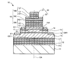
- FIG. 3 is a cross-sectional view of the surface emitting laser according to Example 1.
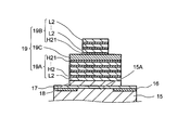
- FIG. 5 is a side view of a second multilayer-film reflective mirror in the surface-emitting laser according to Example 1.
- FIG. 5A to 5D are diagrams showing a method of manufacturing the surface emitting laser according to the first embodiment.
- 5A to 5D are diagrams showing a method of manufacturing the surface emitting laser according to the first embodiment.
- FIG. 6 is a diagram showing the degree of mirror loss in the first multilayer film of the second multilayer film reflecting mirror in the surface emitting laser according to Example 1.
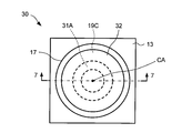
- 5 is a top view of the surface emitting laser according to Example 2.
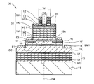
- FIG. 5 is a cross-sectional view of a surface emitting laser according to Example 2.
- FIG. 7 is a top view of a surface emitting laser according to a third embodiment.
- 5 is a cross-sectional view of a surface emitting laser according to Example 3.
- FIG. 9 is a side view of a second multilayer-film reflective mirror in the surface emitting laser according to Example 3.
- FIG. 1 is a schematic top view of a vertical cavity surface emitting laser (VCSEL: Vertical Cavity Surface Emitting Laser, hereinafter referred to as a surface emitting laser) according to the first embodiment.
- VCSEL Vertical Cavity Surface Emitting Laser
- FIG. 2 is a cross-sectional view of the surface emitting laser 10.
- FIG. 2 is a sectional view taken along line 2-2 of FIG. The configuration of the surface emitting laser 10 will be described with reference to FIGS. 1 and 2.
- the surface emitting laser 10 has a substrate 11 and a first multilayer-film reflective mirror (hereinafter, simply referred to as a first reflective mirror) 12 formed on the substrate 11.
- the first reflecting mirror 12 is formed on the substrate 11 and has a lower refractive index than the first semiconductor film (hereinafter, referred to as a high refractive index semiconductor film) H1 and the high refractive index semiconductor film H1.
- the first reflecting mirror 12 constitutes a distributed Bragg reflector (DBR) made of a semiconductor material.
- DBR distributed Bragg reflector
- the n-type semiconductor layer 13 has a composition of GaN and contains Si as an n-type impurity.
- the light emitting layer 14 has a quantum well structure including a well layer having a composition of InGaN and a barrier layer having a composition of GaN.
- the p-type semiconductor layer 15 has a GaN-based composition and contains Mg as a p-type impurity.
- the configuration of the light emitting structure layer EM1 is not limited to this.
- the n-type semiconductor layer 13 may include a plurality of n-type semiconductor layers having different compositions.
- the p-type semiconductor layer 15 may have a plurality of p-type semiconductor layers having different compositions.
- the p-type semiconductor layer 15 has a convex portion 15A on the upper surface.
- the convex portion 15A has a cylindrical shape.
- the surface-emitting laser 10 also has an insulating layer (first insulating layer) 16 formed on the upper surface of the p-type semiconductor layer 15 other than the convex portions 15A.
- the insulating layer 16 is made of a material that is transparent to the light emitted from the light emitting layer 14 and has a refractive index lower than that of the p-type semiconductor layer 15 (recess 15A), for example, an oxide such as SiO 2. Become.
- the p-type semiconductor layer 15 is exposed from the insulating layer 16 on the upper end surface of the convex portion 15A.
- the surface emitting laser 10 has a second multilayer-film reflective mirror (hereinafter, simply referred to as a second reflective mirror) 19 formed on the insulating layer 18.
- the second reflecting mirror 19 is arranged at a position facing the first reflecting film 12 with the light emitting structure layer EM1 interposed therebetween.
- the second reflecting mirror 19 constitutes, together with the first reflecting mirror 12, a resonator OC1 having a resonator length direction in a direction perpendicular to the light emitting structure layer EM1 (direction perpendicular to the substrate 11).
- the second reflecting mirror 19 constitutes a distributed Bragg reflector (DBR) made of a dielectric material.
- DBR distributed Bragg reflector
- the high refractive index dielectric film H2 is made of an Nb 2 O 5 film and the low refractive index dielectric film L2 is made of a SiO 2 film.
- the intermediate dielectric film 19C is formed in the second reflecting mirror 19 in the middle of the high refractive index dielectric film H2.
- the first multilayer film 19A has a high-refractive-index dielectric film (hereinafter, referred to as a first low-film) having a thickness half that of the high-refractive-index dielectric film H2 on the upper surface thereof. Thick high refractive index dielectric film) H21.
- the intermediate dielectric film 19C is formed on the first low-thickness, high-refractive index dielectric film H21.
- the second multilayer film 19B has a high-refractive index dielectric film (second high-refractive index dielectric film) H21 at the interface with the intermediate dielectric film 19C.
- the second multilayer film 19B has a width smaller than that of the intermediate dielectric film 19C.
- the second multilayer film 19B is formed coaxially with the first multilayer film 19A and the intermediate dielectric film 19C, and is smaller than the first multilayer film 19A and the intermediate dielectric film 19C. It has a cylindrical shape with a diameter.
- the surface emitting laser 10 has a cross-sectional shape corresponding to the shape of the first multilayer film 19A of the second reflecting mirror 19, and a cylindrical shape in the present embodiment. It has a resonator OC1.
- the surface emitting laser 10 has a metal film 20 formed on the second reflecting mirror 19.
- the metal film 20 has reflectivity for the light emitted from the light emitting layer 14.
- the metal film 20 includes a first metal film 21 that covers the upper surface of the second multilayer film 19B and a second metal film 22 that covers the upper surface region of the intermediate dielectric film 19C exposed from the second multilayer film 19B. And, including.
- the metal film 20 is made of a metal material such as Ti, Cr, Ni, Pt, Au, Sn.
- the surface emitting laser 10 also has first and second electrodes E1 and E2 for applying a current to the light emitting structure layer EM1.
- the first electrode E1 is formed on the n-type semiconductor layer 13.
- the second electrode E2 is formed on the transparent electrode layer 17.
- the light emitting region of the light emitting layer 14 is, for example, a region having a predetermined width in the light emitting layer 14 in which light having a predetermined intensity or higher is emitted, and the center thereof is the light emission center. Further, for example, the light emitting region of the light emitting layer 14 is a region in the light emitting layer 14 into which a current having a predetermined density or more is injected, and the center thereof is the light emitting center.
- a straight line that passes through the emission center and is perpendicular to the substrate 11 is the central axis CA.
- the central axis CA is a straight line extending along the resonator length direction of the resonator OC1 constituted by the first and second reflecting mirrors 12 and 19.
- the center axis CA corresponds to the optical axis of the laser light emitted from the surface emitting laser 10.
- FIG. 3 is a side view of the second reflecting mirror 19.
- the detailed configuration of the second reflecting mirror 19 will be described with reference to FIG.
- the low-refractive-index dielectric film L2 and the high-refractive-index dielectric film H2 are stacked four times in this order on the insulating layer 18, and the uppermost low-refractive-index dielectric film L2. It has a structure in which the first low-film-thickness high-refractive-index dielectric layer H21 is formed thereon.
- the intermediate dielectric film 19C has a smaller etching rate than the other dielectric films in the second reflecting mirror 19. Therefore, when the second multilayer film 19BP is etched, the etching can be reliably stopped in the middle of the intermediate dielectric film 19C. That is, for example, in the portion to be etched, the dielectric film at the bottom of the second multilayer film 19BP is not partially left, and the first multilayer film 19A is not partially etched, so that the second multilayer film 19BP can be stably Only the multilayer film 19BP can be etched.
- the etching accuracy will be significantly stable. Therefore, the multilayer film can be processed so that the etching stops at the designed depth position or the designed film position. In this embodiment, the reflection characteristic of the second reflecting mirror 19 can be adjusted stably.
- the metal film 20 is formed on the intermediate dielectric film 19C and the second multilayer film 19B (step 5).
- the first and second electrodes E1 and E2 are formed on the n-type semiconductor layer 13 and the p-type semiconductor layer 15 of the light emitting structure layer EM1 (step 6). In this way, the surface emitting laser 10 can be manufactured.
- the high-refractive-index dielectric film H2 of the sixth pair is divided into the first and second low-thickness high-refractive-index dielectric films H21(6).
- the intermediate dielectric film 19C between the two so that the etching is stopped in the middle of the process, the second multilayer film 19B can be stably removed, and a large mirror loss can be caused at the removed portion. it can.
- the second multilayer film 19B is formed in the central portion of the first multilayer film 19A within the plane of the first multilayer film 19A. That is, the second multilayer film 19B is removed from the outer peripheral portion of the first multilayer film 19A.
- the first and second multilayer films 19A and 19B are provided on the central axis CA of the resonator OC1. As a result, it is possible to stably increase the mirror loss in the peripheral region of the region including the central axis CA of the resonator OC1.
- the second reflecting mirror 19 is a DBR made of a dielectric material.
- the second reflecting mirror 19 may be a multilayer-film reflecting mirror, and its material is not limited to a dielectric.
- the position of the intermediate dielectric film 19C may be provided at any preferable position in the second reflecting mirror 19.
- the upper surface of the second reflecting mirror 19 is covered with the metal film 20, between the first and second low-thickness high-refractive index films H21 provided in the first and second multilayer films 19A and 19B, respectively. Is preferably provided in the.
- the low-refractive-index dielectric film L2 is provided closest to the substrate 11 in the first multilayer film 19A, and the high-refractive index dielectric film L2 is provided near the intermediate dielectric film 19C in the first multilayer film 19A.
- a low-thickness high-refractive-index dielectric film H21 made of a refractive index material and having a smaller film thickness than the high-refractive-index dielectric film H2 is provided.
- the intermediate dielectric film 19C has a thickness based on 1/2 of the wavelength of the light emitted from the light emitting layer 14 in the intermediate dielectric film 19C. Therefore, it is possible to provide the surface emitting laser 10 (vertical cavity type light emitting element) capable of emitting stable transverse mode light.
- the second reflecting mirror 31 is replaced with the second reflecting mirror 19B of the second reflecting mirror 19 and has a second multilayer film 31A formed in a ring shape on the upper surface of the intermediate dielectric film 19C.
- the second multilayer film 31A has a high-refractive index dielectric film H2 and a low-refractive index dielectric film L2 formed in an annular shape.
- the metal film 32 is formed on the intermediate dielectric film 19C and the second multilayer film 31A including the upper surface of the intermediate dielectric film 31A exposed from the second multilayer film 31 inside the second multilayer film 31. Has been done.
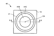
- FIG. 8 is a top view of the surface emitting laser 40 according to the third embodiment.
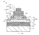
- FIG. 9 is a sectional view of the surface emitting laser 40.
- the surface emitting laser 40 has the same configuration as the surface emitting laser 10 except for the configuration of the second reflecting mirror 41. In the surface emitting laser 40, the second reflecting mirror 41 is optically exposed on the upper surface.
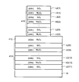
- the second reflecting mirror 41 includes a first multilayer film 41A having a low refractive index layer L2 on the uppermost surface and an intermediate layer formed on the low refractive index layer L2 of the first multilayer film 41A. It has a dielectric film 41C and a second multilayer film 41B formed on the intermediate dielectric film 41C and having a high refractive index layer H2 at the interface with the intermediate dielectric film 41C. Further, no metal film is provided on the upper surfaces of the second multilayer film 41B and the intermediate dielectric film 41C, and they are optically exposed.
- the intermediate dielectric film 41C is the high-refractive-index dielectric film that is the fifth pair from the upper surface of the second multilayer film 41B in the second reflecting mirror 41. It is formed between H2(5) and the sixth low-refractive-index dielectric film L2(6).
- the upper surface of the second reflecting mirror 41 is optically exposed, and the light reflection condition at the end face is different from the case where a metal film is provided.
- a large mirror loss can be generated by providing the intermediate dielectric film 41C at the above position and etching. Therefore, for example, a single-peaked laser beam can be stably emitted.
- the second multilayer film 41B has five low-refractive-index dielectric films L2 and high-refractive-index dielectric films H2, respectively, and the low-refractive-index dielectric film L2.
- the high-refractive-index dielectric film H2 and the high-refractive-index dielectric film H2 have a film thickness (for example, ⁇ x It is preferable to have a film thickness satisfying /4n (x is a natural number).
- a reflecting mirror having a preferable reflection characteristic is formed. It is possible to provide, for example, stable lateral mode surface emitting lasers 10, 30 and 40 (vertical cavity type light emitting device).
Landscapes
- Physics & Mathematics (AREA)
- Condensed Matter Physics & Semiconductors (AREA)
- General Physics & Mathematics (AREA)
- Electromagnetism (AREA)
- Optics & Photonics (AREA)
- Geometry (AREA)
- Semiconductor Lasers (AREA)
Abstract
Description
EM1 発光構造層
14 発光層
19、31、41 第2の多層膜反射鏡
Claims (9)
- 基板と、
前記基板上に形成された第1の多層膜反射鏡と、
前記第1の多層膜反射鏡上に形成され、発光層を含む発光構造層と、
前記発光構造層上に形成され、前記第1の多層膜反射鏡との間で共振器を構成する第2の多層膜反射鏡と、を有し、
前記第2の多層膜反射鏡は、低屈折率材料からなる低屈折率膜と前記低屈折率材料よりも大きな屈折率を有する高屈折率材料からなる高屈折率膜とが交互に積層された第1の多層膜と、前記第1の多層膜の上面を覆いかつ前記発光層から放出された光に対して透光性を有する中間膜と、前記中間膜の上面を部分的に覆うように形成され、前記低屈折率材料からなる低屈折率膜と前記高屈折率材料からなる高屈折率膜とが交互に積層された第2の多層膜と、を含み、
前記中間膜は、前記発光層から放出される光の前記中間膜内の波長の1/2に基づいた膜厚を有することを特徴とする垂直共振器型発光素子。 - 前記第1の多層膜の最も前記基板側には低屈折率膜が設けられ、前記第1の多層膜の最も前記中間膜側には前記高屈折率材料からなりかつ前記高屈折率膜よりも小さな膜厚を有する低膜厚高屈折率膜が設けられ、
前記第2の多層膜の最も上面側には低屈折率膜が設けられ、前記第2の多層膜の最も前記中間膜側には前記高屈折率材料からなりかつ前記高屈折率膜よりも小さな膜厚を有する低膜厚高屈折率膜が設けられ、
前記第2の多層膜及び前記中間膜の上面は金属膜に覆われていることを特徴とする請求項1に記載の垂直共振器型発光素子。 - 前記第2の多層膜は、それぞれ5つの低屈折率膜及び高屈折率膜と、前記低膜厚高屈折率膜と、を有し、
前記第1及び第2の多層膜における前記低屈折率膜及び前記高屈折率膜は、前記発光層から放出された光のそれぞれ前記低屈折率膜及び前記高屈折率膜内の波長の1/4に基づいた膜厚を有し、
前記第1及び第2の多層膜における前記低膜厚高屈折率膜は、前記発光層から放出された光の前記低膜厚高屈折率膜内の波長の1/8に基づいた膜厚を有することを特徴とする請求項2に記載の垂直共振器型発光素子。 - 前記第1の多層膜の最も前記基板側には低屈折率膜が設けられ、前記第1の多層膜の最も前記中間膜側には低屈折率膜が設けられ、
前記第2の多層膜の最も上面側には低屈折率膜が設けられ、前記第2の多層膜の最も前記中間膜側には高屈折率膜が設けられ、
前記第2の多層膜及び前記中間膜の上面は光学的に露出していることを特徴とする請求項1に記載の垂直共振器型発光素子。 - 前記第2の多層膜は、それぞれ5つの低屈折率膜及び高屈折率膜を有し、
前記第1及び第2の多層膜における前記低屈折率膜及び前記高屈折率膜は、前記発光層から放出された光のそれぞれ前記低屈折率膜及び前記高屈折率膜内の波長の1/4に基づいた膜厚を有することを特徴とする請求項4に記載の垂直共振器型発光素子。 - 前記第2の多層膜は、前記中間膜の上面において環状に形成されていることを特徴とする請求項1に記載の垂直共振器型発光素子。
- 前記中間膜は、前記第2の多層膜の前記低屈折率膜及び前記高屈折率膜よりも小さなエッチング速度を有することを特徴とする請求項1乃至6のいずれか1つに記載の垂直共振器型発光素子。
- 前記高屈折率膜、前記低屈折率膜及び前記中間膜は、誘電体膜からなることを特徴とする請求項1乃至7のいずれか1つに記載の垂直共振器型発光素子。
- 前記中間膜は、Al2O3膜又はAlN膜からなることを特徴とする請求項8に記載の垂直共振器型発光素子。
Priority Applications (3)
| Application Number | Priority Date | Filing Date | Title |
|---|---|---|---|
| CN202080015818.4A CN113491045B (zh) | 2019-02-21 | 2020-01-20 | 垂直腔面发光器件 |
| US17/432,466 US12266906B2 (en) | 2019-02-21 | 2020-01-20 | Vertical cavity surface emitting device |
| EP20759298.1A EP3930121B1 (en) | 2019-02-21 | 2020-01-20 | Vertical cavity light-emitting element |
Applications Claiming Priority (2)
| Application Number | Priority Date | Filing Date | Title |
|---|---|---|---|
| JP2019029293A JP7258591B2 (ja) | 2019-02-21 | 2019-02-21 | 垂直共振器型発光素子 |
| JP2019-029293 | 2019-02-21 |
Publications (1)
| Publication Number | Publication Date |
|---|---|
| WO2020170675A1 true WO2020170675A1 (ja) | 2020-08-27 |
Family
ID=72143447
Family Applications (1)
| Application Number | Title | Priority Date | Filing Date |
|---|---|---|---|
| PCT/JP2020/001693 Ceased WO2020170675A1 (ja) | 2019-02-21 | 2020-01-20 | 垂直共振器型発光素子 |
Country Status (5)
| Country | Link |
|---|---|
| US (1) | US12266906B2 (ja) |
| EP (1) | EP3930121B1 (ja) |
| JP (1) | JP7258591B2 (ja) |
| CN (1) | CN113491045B (ja) |
| WO (1) | WO2020170675A1 (ja) |
Families Citing this family (5)
| Publication number | Priority date | Publication date | Assignee | Title |
|---|---|---|---|---|
| JP7166871B2 (ja) | 2018-10-18 | 2022-11-08 | スタンレー電気株式会社 | 垂直共振器型発光素子 |
| JP7190865B2 (ja) * | 2018-10-18 | 2022-12-16 | スタンレー電気株式会社 | 垂直共振器型発光素子 |
| EP4089860B1 (en) | 2020-01-08 | 2025-02-26 | Stanley Electric Co., Ltd. | Vertical-resonator-type light-emitting element |
| JP7742724B2 (ja) * | 2021-06-07 | 2025-09-22 | スタンレー電気株式会社 | 垂直共振器型発光素子及びその製造方法 |
| WO2025177929A1 (ja) * | 2024-02-19 | 2025-08-28 | ソニーセミコンダクタソリューションズ株式会社 | 面発光素子 |
Citations (8)
| Publication number | Priority date | Publication date | Assignee | Title |
|---|---|---|---|---|
| JPS577742B2 (ja) | 1977-05-16 | 1982-02-12 | ||
| US6751245B1 (en) * | 1999-06-02 | 2004-06-15 | Optical Communication Products, Inc. | Single mode vertical cavity surface emitting laser |
| JP2005353623A (ja) * | 2004-06-08 | 2005-12-22 | Ricoh Co Ltd | 面発光レーザ及び光伝送システム |
| JP2014036027A (ja) * | 2012-08-07 | 2014-02-24 | Fuji Xerox Co Ltd | 面発光型半導体レーザ、面発光型半導体レーザ装置、光伝送装置および情報処理装置 |
| JP2016004944A (ja) * | 2014-06-18 | 2016-01-12 | 古河電気工業株式会社 | 面発光レーザ素子 |
| US20160134083A1 (en) * | 2014-11-06 | 2016-05-12 | The Board Of Trustees Of The University Of Illinois | Mode Control in Vertical-Cavity Surface-Emitting Lasers |
| US20170214218A1 (en) * | 2014-09-22 | 2017-07-27 | Hewlett Packard Enterprise Development Lp | Single mode vertical-cavity surface-emitting laser |
| JP2017204579A (ja) * | 2016-05-12 | 2017-11-16 | スタンレー電気株式会社 | 垂直共振器型発光素子及び垂直共振器型発光素子の製造方法 |
Family Cites Families (19)
| Publication number | Priority date | Publication date | Assignee | Title |
|---|---|---|---|---|
| US6845118B1 (en) * | 1999-01-25 | 2005-01-18 | Optical Communication Products, Inc. | Encapsulated optoelectronic devices with controlled properties |
| JP3422413B2 (ja) * | 1999-04-09 | 2003-06-30 | 日本電気株式会社 | 面発光型レーザアレイ及びその製造方法 |
| US6727520B2 (en) * | 2000-12-29 | 2004-04-27 | Honeywell International Inc. | Spatially modulated reflector for an optoelectronic device |
| JP4629949B2 (ja) * | 2002-04-05 | 2011-02-09 | 古河電気工業株式会社 | 面発光レーザ素子、面発光レーザ素子を用いたトランシーバ、光送受信器および光通信システム |
| GB2399940A (en) * | 2003-03-25 | 2004-09-29 | Sharp Kk | Vertical cavity surface emitting laser |
| CN101432936B (zh) | 2004-10-01 | 2011-02-02 | 菲尼萨公司 | 具有多顶侧接触的垂直腔面发射激光器 |
| JP2008211164A (ja) | 2007-01-29 | 2008-09-11 | Matsushita Electric Ind Co Ltd | 窒化物半導体発光装置及びその製造方法 |
| EP2210319B1 (en) | 2007-11-14 | 2020-10-07 | Ricoh Company, Ltd. | Surface emitting laser, surface emitting laser array, optical scanning device, image forming apparatus, optical transmission module and optical transmission system |
| JP5279393B2 (ja) * | 2008-07-31 | 2013-09-04 | キヤノン株式会社 | 面発光レーザおよびその製造方法、面発光レーザアレイの製造方法、および面発光レーザアレイを備えている光学機器 |
| JP5707742B2 (ja) | 2009-06-30 | 2015-04-30 | 日亜化学工業株式会社 | 垂直共振器型面発光レーザ |
| EP2533380B8 (en) * | 2011-06-06 | 2017-08-30 | Mellanox Technologies, Ltd. | High speed lasing device |
| JP2016027648A (ja) * | 2014-06-30 | 2016-02-18 | キヤノン株式会社 | 面発光レーザ、及び前記面発光レーザを用いた光干渉断層計 |
| JP6743369B2 (ja) | 2014-11-12 | 2020-08-19 | 株式会社リコー | 面発光レーザ、面発光レーザアレイ、光走査装置及び画像形成装置 |
| JP6700027B2 (ja) | 2015-11-20 | 2020-05-27 | スタンレー電気株式会社 | 垂直共振器型発光素子 |
| US10700494B2 (en) * | 2016-04-01 | 2020-06-30 | Hewlett Packard Enterprise Development Lp | Data center transmission systems |
| JP6990499B2 (ja) | 2016-04-18 | 2022-01-12 | スタンレー電気株式会社 | 垂直共振器型発光素子及び垂直共振型発光素子の製造方法 |
| JP2018073853A (ja) | 2016-10-24 | 2018-05-10 | スタンレー電気株式会社 | 反射鏡、垂直共振器型発光装置及びその製造方法 |
| JP6966843B2 (ja) | 2017-02-08 | 2021-11-17 | スタンレー電気株式会社 | 垂直共振器型発光素子 |
| US10892601B2 (en) | 2018-05-24 | 2021-01-12 | Stanley Electric Co., Ltd. | Vertical cavity light-emitting element |
-
2019
- 2019-02-21 JP JP2019029293A patent/JP7258591B2/ja active Active
-
2020
- 2020-01-20 EP EP20759298.1A patent/EP3930121B1/en active Active
- 2020-01-20 WO PCT/JP2020/001693 patent/WO2020170675A1/ja not_active Ceased
- 2020-01-20 CN CN202080015818.4A patent/CN113491045B/zh active Active
- 2020-01-20 US US17/432,466 patent/US12266906B2/en active Active
Patent Citations (8)
| Publication number | Priority date | Publication date | Assignee | Title |
|---|---|---|---|---|
| JPS577742B2 (ja) | 1977-05-16 | 1982-02-12 | ||
| US6751245B1 (en) * | 1999-06-02 | 2004-06-15 | Optical Communication Products, Inc. | Single mode vertical cavity surface emitting laser |
| JP2005353623A (ja) * | 2004-06-08 | 2005-12-22 | Ricoh Co Ltd | 面発光レーザ及び光伝送システム |
| JP2014036027A (ja) * | 2012-08-07 | 2014-02-24 | Fuji Xerox Co Ltd | 面発光型半導体レーザ、面発光型半導体レーザ装置、光伝送装置および情報処理装置 |
| JP2016004944A (ja) * | 2014-06-18 | 2016-01-12 | 古河電気工業株式会社 | 面発光レーザ素子 |
| US20170214218A1 (en) * | 2014-09-22 | 2017-07-27 | Hewlett Packard Enterprise Development Lp | Single mode vertical-cavity surface-emitting laser |
| US20160134083A1 (en) * | 2014-11-06 | 2016-05-12 | The Board Of Trustees Of The University Of Illinois | Mode Control in Vertical-Cavity Surface-Emitting Lasers |
| JP2017204579A (ja) * | 2016-05-12 | 2017-11-16 | スタンレー電気株式会社 | 垂直共振器型発光素子及び垂直共振器型発光素子の製造方法 |
Non-Patent Citations (1)
| Title |
|---|
| See also references of EP3930121A4 |
Also Published As
| Publication number | Publication date |
|---|---|
| JP7258591B2 (ja) | 2023-04-17 |
| EP3930121A1 (en) | 2021-12-29 |
| US20220149595A1 (en) | 2022-05-12 |
| US12266906B2 (en) | 2025-04-01 |
| JP2020136523A (ja) | 2020-08-31 |
| EP3930121A4 (en) | 2022-12-21 |
| CN113491045B (zh) | 2025-01-10 |
| EP3930121B1 (en) | 2025-11-12 |
| CN113491045A (zh) | 2021-10-08 |
Similar Documents
| Publication | Publication Date | Title |
|---|---|---|
| JP7586446B2 (ja) | 垂直共振器型発光素子 | |
| JP7212882B2 (ja) | 垂直共振器型発光素子 | |
| WO2020170675A1 (ja) | 垂直共振器型発光素子 | |
| US7697588B2 (en) | Structure having photonic crystal and surface-emitting laser using the same | |
| US9368937B1 (en) | Multimode vertical cavity surface emitting laser having narrow laser light emitting angle | |
| CN101145674A (zh) | 垂直腔面发射激光器及其制造方法 | |
| JP2001156395A (ja) | 面発光半導体レーザ素子 | |
| JP7288360B2 (ja) | 垂直共振器型発光素子 | |
| WO2018221042A1 (ja) | 発光素子および発光素子の製造方法 | |
| CN112913094A (zh) | 垂直谐振器式发光元件 | |
| JP7696887B2 (ja) | 半導体レーザ素子 | |
| WO2020080161A1 (ja) | 垂直共振器型発光素子 | |
| JP7623563B2 (ja) | 垂直共振器面発光レーザ素子 | |
| US10256609B2 (en) | Surface light-emitting laser | |
| TW201906263A (zh) | 面發光半導體雷射及感測模組 | |
| JP7227469B2 (ja) | 垂直共振器面発光レーザ素子 | |
| JP6015220B2 (ja) | 面発光型半導体レーザ、面発光型半導体レーザ装置、光伝送装置および情報処理装置 | |
| JPWO2004082085A1 (ja) | 多波長半導体レーザ装置及びその製造方法 | |
| JP2010045249A (ja) | 半導体発光素子およびその製造方法 | |
| JP7081000B2 (ja) | 垂直共振器型発光素子 | |
| JP2017118034A (ja) | 垂直共振器型発光素子 | |
| JP2007227861A (ja) | 半導体発光素子 | |
| JP2024121885A (ja) | 垂直共振器型発光素子及び垂直共振器型発光素子の製造方法 |
Legal Events
| Date | Code | Title | Description |
|---|---|---|---|
| 121 | Ep: the epo has been informed by wipo that ep was designated in this application |
Ref document number: 20759298 Country of ref document: EP Kind code of ref document: A1 |
|
| NENP | Non-entry into the national phase |
Ref country code: DE |
|
| ENP | Entry into the national phase |
Ref document number: 2020759298 Country of ref document: EP Effective date: 20210921 |
|
| WWG | Wipo information: grant in national office |
Ref document number: 202080015818.4 Country of ref document: CN |
|
| WWG | Wipo information: grant in national office |
Ref document number: 17432466 Country of ref document: US |
|
| WWG | Wipo information: grant in national office |
Ref document number: 2020759298 Country of ref document: EP |