WO2020170822A1 - Élément de support de carte et ensemble connecteur pour carte - Google Patents
Élément de support de carte et ensemble connecteur pour carte Download PDFInfo
- Publication number
- WO2020170822A1 WO2020170822A1 PCT/JP2020/004357 JP2020004357W WO2020170822A1 WO 2020170822 A1 WO2020170822 A1 WO 2020170822A1 JP 2020004357 W JP2020004357 W JP 2020004357W WO 2020170822 A1 WO2020170822 A1 WO 2020170822A1
- Authority
- WO
- WIPO (PCT)
- Prior art keywords
- tray
- card
- connector
- terminal
- holding member
- Prior art date
- Legal status (The legal status is an assumption and is not a legal conclusion. Google has not performed a legal analysis and makes no representation as to the accuracy of the status listed.)
- Ceased
Links
Images


Classifications
-
- H—ELECTRICITY
- H01—ELECTRIC ELEMENTS
- H01R—ELECTRICALLY-CONDUCTIVE CONNECTIONS; STRUCTURAL ASSOCIATIONS OF A PLURALITY OF MUTUALLY-INSULATED ELECTRICAL CONNECTING ELEMENTS; COUPLING DEVICES; CURRENT COLLECTORS
- H01R12/00—Structural associations of a plurality of mutually-insulated electrical connecting elements, specially adapted for printed circuits, e.g. printed circuit boards [PCB], flat or ribbon cables, or like generally planar structures, e.g. terminal strips, terminal blocks; Coupling devices specially adapted for printed circuits, flat or ribbon cables, or like generally planar structures; Terminals specially adapted for contact with, or insertion into, printed circuits, flat or ribbon cables, or like generally planar structures
- H01R12/70—Coupling devices
- H01R12/7005—Guiding, mounting, polarizing or locking means; Extractors
-
- G—PHYSICS
- G06—COMPUTING OR CALCULATING; COUNTING
- G06K—GRAPHICAL DATA READING; PRESENTATION OF DATA; RECORD CARRIERS; HANDLING RECORD CARRIERS
- G06K7/00—Methods or arrangements for sensing record carriers, e.g. for reading patterns
- G06K7/0013—Methods or arrangements for sensing record carriers, e.g. for reading patterns by galvanic contacts, e.g. card connectors for ISO-7816 compliant smart cards or memory cards, e.g. SD card readers
- G06K7/0034—Methods or arrangements for sensing record carriers, e.g. for reading patterns by galvanic contacts, e.g. card connectors for ISO-7816 compliant smart cards or memory cards, e.g. SD card readers the connector being capable of simultaneously receiving a plurality of cards in the same insertion slot
- G06K7/0039—Methods or arrangements for sensing record carriers, e.g. for reading patterns by galvanic contacts, e.g. card connectors for ISO-7816 compliant smart cards or memory cards, e.g. SD card readers the connector being capable of simultaneously receiving a plurality of cards in the same insertion slot the plurality of cards being cards of the same type and format, e.g. two ISO 7816 smart cards
-
- G—PHYSICS
- G06—COMPUTING OR CALCULATING; COUNTING
- G06K—GRAPHICAL DATA READING; PRESENTATION OF DATA; RECORD CARRIERS; HANDLING RECORD CARRIERS
- G06K19/00—Record carriers for use with machines and with at least a part designed to carry digital markings
- G06K19/06—Record carriers for use with machines and with at least a part designed to carry digital markings characterised by the kind of the digital marking, e.g. shape, nature, code
- G06K19/067—Record carriers with conductive marks, printed circuits or semiconductor circuit elements, e.g. credit or identity cards also with resonating or responding marks without active components
- G06K19/07—Record carriers with conductive marks, printed circuits or semiconductor circuit elements, e.g. credit or identity cards also with resonating or responding marks without active components with integrated circuit chips
- G06K19/077—Constructional details, e.g. mounting of circuits in the carrier
- G06K19/07743—External electrical contacts
-
- G—PHYSICS
- G06—COMPUTING OR CALCULATING; COUNTING
- G06K—GRAPHICAL DATA READING; PRESENTATION OF DATA; RECORD CARRIERS; HANDLING RECORD CARRIERS
- G06K7/00—Methods or arrangements for sensing record carriers, e.g. for reading patterns
- G06K7/0013—Methods or arrangements for sensing record carriers, e.g. for reading patterns by galvanic contacts, e.g. card connectors for ISO-7816 compliant smart cards or memory cards, e.g. SD card readers
- G06K7/0056—Methods or arrangements for sensing record carriers, e.g. for reading patterns by galvanic contacts, e.g. card connectors for ISO-7816 compliant smart cards or memory cards, e.g. SD card readers housing of the card connector
- G06K7/006—Methods or arrangements for sensing record carriers, e.g. for reading patterns by galvanic contacts, e.g. card connectors for ISO-7816 compliant smart cards or memory cards, e.g. SD card readers housing of the card connector the housing being a portable casing
-
- G—PHYSICS
- G06—COMPUTING OR CALCULATING; COUNTING
- G06K—GRAPHICAL DATA READING; PRESENTATION OF DATA; RECORD CARRIERS; HANDLING RECORD CARRIERS
- G06K7/00—Methods or arrangements for sensing record carriers, e.g. for reading patterns
- G06K7/0013—Methods or arrangements for sensing record carriers, e.g. for reading patterns by galvanic contacts, e.g. card connectors for ISO-7816 compliant smart cards or memory cards, e.g. SD card readers
- G06K7/0056—Methods or arrangements for sensing record carriers, e.g. for reading patterns by galvanic contacts, e.g. card connectors for ISO-7816 compliant smart cards or memory cards, e.g. SD card readers housing of the card connector
- G06K7/0073—Methods or arrangements for sensing record carriers, e.g. for reading patterns by galvanic contacts, e.g. card connectors for ISO-7816 compliant smart cards or memory cards, e.g. SD card readers housing of the card connector having multiple insertion slots, the respective slots suited for the same or different card form factors
-
- H—ELECTRICITY
- H01—ELECTRIC ELEMENTS
- H01R—ELECTRICALLY-CONDUCTIVE CONNECTIONS; STRUCTURAL ASSOCIATIONS OF A PLURALITY OF MUTUALLY-INSULATED ELECTRICAL CONNECTING ELEMENTS; COUPLING DEVICES; CURRENT COLLECTORS
- H01R12/00—Structural associations of a plurality of mutually-insulated electrical connecting elements, specially adapted for printed circuits, e.g. printed circuit boards [PCB], flat or ribbon cables, or like generally planar structures, e.g. terminal strips, terminal blocks; Coupling devices specially adapted for printed circuits, flat or ribbon cables, or like generally planar structures; Terminals specially adapted for contact with, or insertion into, printed circuits, flat or ribbon cables, or like generally planar structures
- H01R12/70—Coupling devices
- H01R12/71—Coupling devices for rigid printing circuits or like structures
- H01R12/712—Coupling devices for rigid printing circuits or like structures co-operating with the surface of the printed circuit or with a coupling device exclusively provided on the surface of the printed circuit
- H01R12/714—Coupling devices for rigid printing circuits or like structures co-operating with the surface of the printed circuit or with a coupling device exclusively provided on the surface of the printed circuit with contacts abutting directly the printed circuit; Button contacts therefore provided on the printed circuit
-
- H—ELECTRICITY
- H01—ELECTRIC ELEMENTS
- H01R—ELECTRICALLY-CONDUCTIVE CONNECTIONS; STRUCTURAL ASSOCIATIONS OF A PLURALITY OF MUTUALLY-INSULATED ELECTRICAL CONNECTING ELEMENTS; COUPLING DEVICES; CURRENT COLLECTORS
- H01R12/00—Structural associations of a plurality of mutually-insulated electrical connecting elements, specially adapted for printed circuits, e.g. printed circuit boards [PCB], flat or ribbon cables, or like generally planar structures, e.g. terminal strips, terminal blocks; Coupling devices specially adapted for printed circuits, flat or ribbon cables, or like generally planar structures; Terminals specially adapted for contact with, or insertion into, printed circuits, flat or ribbon cables, or like generally planar structures
- H01R12/70—Coupling devices
- H01R12/71—Coupling devices for rigid printing circuits or like structures
- H01R12/72—Coupling devices for rigid printing circuits or like structures coupling with the edge of the rigid printed circuits or like structures
- H01R12/73—Coupling devices for rigid printing circuits or like structures coupling with the edge of the rigid printed circuits or like structures connecting to other rigid printed circuits or like structures
Definitions
- the present disclosure relates to a card holding member and a card connector set.
- FIG. 13 is a diagram showing a conventional card connector.
- 811 is a substrate of a card connector on the surface of which conductive connecting pads (not shown) are formed
- 861 is a shell of the card connector made of a metal plate, and covers the upper part of the connecting pad.
- the card housing space 818 of the card connector is formed between the board 811 and the shell 861.
- Reference numeral 971 denotes a card tray, which is inserted from the entrance side of the card housing space 818 as shown by an arrow in a state where the card 901 is loaded inside and is housed in the card connector.
- a plurality of conductive members 951 are attached to the bottom plate of the card tray 971.
- the card 901 When the card 901 is loaded on the card tray 971, it is exposed and formed on the lower surface of the card 901.
- Each of the plurality of electrode pads contacts the upper surface of the corresponding conductive member 951.
- the lower surface of the tip of each conductive member 951 contacts the connection pad formed on the surface of the substrate 811.
- the electrode pad and the corresponding connection pad of the card connector are connected via the conductive member 951.
- the card 901 is inserted and accommodated in the card accommodation space 818 while being loaded in the card tray 971. Therefore, when the card 901 is accommodated in the card accommodation space 818, the card 901 is accommodated in the card accommodation space 818. There is no contact with the entrance of the space 818, and the electrode pads and the like are not damaged. Moreover, since the electrode pad of the card 901 and the corresponding connection pad are connected via the conductive member 951 having elasticity, the electrical connection between the electrode pad and the connection pad is stabilized.
- the conductive member 951 attached to the bottom plate of the card tray 971 is elastically deformed to maintain contact with the electrode pad of the card 901, and Since the contact with the connection pad is maintained, it is necessary to increase the elastically deformable range of the conductive member 951, which makes it difficult to reduce the size of the conductive member 951. It becomes difficult to downsize the 971 and it becomes difficult to downsize the card connector that accommodates the card tray 971.
- the card holding member is a card holding member that can hold a card having an electrode pad and can be inserted into a card connector having a connector terminal, and has a concave portion that can accommodate the card and a concave portion of the concave portion.
- a tray housing including a bottom wall portion defining a bottom surface and a tray terminal accommodating recess formed in the bottom wall portion, and a tray terminal arranged in the bottom wall portion, at least a part of which is the bottom wall. And a first contact portion and a second contact portion, which are respectively connected to both ends of the main body portion and are held by the first and second contact portions, and which are in contact with the connector terminal and the electrode pad.
- a tray terminal including a possible second contact portion, wherein the first contact portion is fixed and exposed on a surface of the bottom wall portion opposite to the bottom surface of the recess, and the second contact portion is At least the contact points of the contacts projecting from the bottom surface of the recess are housed in the tray terminal housing recess so as to be elastically deformable.
- the second contact portion can be elastically deformed in the tray terminal accommodating recess without interfering with another member.
- the tray terminal may form a single row or a plurality of rows in which the second contact portions are arranged in a width direction orthogonal to the insertion direction of the card holding member in plan view. It is installed in.
- the tray terminal is arranged so that the main body portion extends in the insertion direction of the card holding member in a plan view.
- the tray terminal further includes a tray terminal in which the main body portion is arranged so as to extend in the insertion direction of the card holding member in plan view, and the main body portion. And a tray terminal arranged so as to extend in a width direction orthogonal to the insertion direction of the card holding member.
- At least one of the tray terminals includes a row-direction portion in which the main body portion is arranged so as to extend in the insertion direction of the card holding member in plan view,
- the main body portion includes a row direction portion arranged so as to extend in a width direction orthogonal to the insertion direction of the card holding member.
- the tray terminal further includes an inclined direction portion connecting the column direction portion and the row direction portion.
- a card holding member according to the present disclosure and a card connector into which the card holding member can be inserted, the connector including an elastically deformable contact portion that can contact the first contact portion A card connector having terminals.
- each of the connector terminals extends in the insertion direction of the card holding member, and the contact portion, in plan view, the insertion direction of the card holding member and It is arranged so as to form a single row or a plurality of rows arranged along the width direction orthogonal to each other.
- the card holding member and card connector set can be used for cards that are small and thin, and have multiple poles, and can be made compact and have a low profile and multiple poles, thus improving reliability.
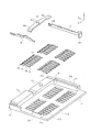
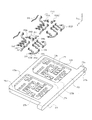
- FIG. 6 is a perspective view showing a card connector set in which a tray for holding a card is inserted into the connector in the first embodiment.
- FIG. 3 is an exploded view of the card connector set according to the first embodiment.
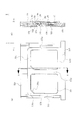
- FIG. 6 is a perspective view showing a state in which a connector cover of the card connector set in which a tray that does not hold a card is inserted in the connector in the first embodiment is removed. It is an exploded view of a portion other than the connector cover of the connector in the first embodiment.
- FIG. 2A is a two-sided view of a card connector set in which a tray for holding a card is inserted in the connector according to the first embodiment
- FIG. 7A is a top view
- FIG. 2A is a two-sided view of the card connector set in which a tray for holding a card is inserted in the connector according to the first embodiment with a connector cover removed, where FIG. FIG. 7 is a sectional view taken along the line AA in (a).
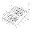
- FIG. 6 is a cross-sectional perspective view of a card connector set in which a tray for holding a card is inserted in the connector according to the first embodiment.
- FIG. 10 is a perspective view of a connector for a card in which a tray that does not hold a card is inserted into a connector in the second embodiment and a connector cover is removed. It is a bottom view of the card in a 2nd embodiment. It is an exploded view of the tray in a 2nd embodiment.
- FIG. 12A is a two-sided view of the card connector set in which the tray is inserted in the connector according to the second embodiment with the connector cover removed
- FIG. 7A is a sectional view taken along the line BB in FIG. 7A and showing a state in which the card is held
- FIG. 8C is a sectional view taken in the direction of CC in FIG. FIG. It is a figure which shows the conventional connector for cards.
- FIG. 1 is a perspective view showing a card connector set in which a tray for holding a card is inserted into a connector in the first embodiment
- FIG. 2 is an exploded view of the card connector set in the first embodiment
- FIG. FIG. 4 is a perspective view showing a state in which a connector cover of a card connector set in which a tray that does not hold a card is inserted into the connector in the first embodiment is removed, and FIG. 4 shows other than the connector cover of the connector in the first embodiment.
- FIG. 5 is an exploded view of a part
- FIG. 5 is a two-sided view of a card connector set in which a tray for holding a card is inserted in the connector in the first embodiment
- FIG. 6 is a drawing in which the card is held in the connector in the first embodiment.
- FIG. 7 is a two-sided view of the card connector set in which the tray for inserting the card is removed
- FIG. 7 is a sectional perspective view of the card connector set in which the tray for holding the card is inserted in the connector according to the first embodiment. It is a figure. 5 and 6, (a) is a top view and (b) is a sectional view taken along the line AA in (a).
- reference numeral 170 denotes a tray as a card holding member in the present embodiment, which is inserted into a connector 1 as a card connector mounted on a circuit board of an electronic device (not shown) in a state where the card 101 is accommodated. As a result, the card 101 is attached to the electronic device via the tray 170 and the connector 1.
- the card connector set is a tray 170 to which the card 101 is electrically connected, and the tray 170 is inserted in the same direction as the plane direction of the circuit board of the electronic device and electrically connected to the tray 170. It will be described as being provided with the connector 1 and used for connecting the card 101 and the electronic device via the card connector set.
- the card 101 is, for example, a SIM card, a micro SIM card, a nano SIM card, an MMC(R), an SD(R) card, a miniSD(R) card, an xD picture card (R), a memory. It may be a memory card itself such as a stick (R), a memory stick Duo (R), a smart media (R), a Trans-Flash (R) memory card, or, for example, a miniSD (R) card inside.
- a card adapter having a shape and dimensions suitable for insertion into the connector 1 and having a memory card accommodated therein may be used, such as an SD(R) card type adapter accommodated.
- the electronic device is, for example, a personal computer, a mobile phone, a smartphone, a communication modem, a pad computer, a digital camera, a video camera, a music player, a game machine, a vehicle navigation device, etc. It may be.
- the circuit board of the electronic device is a printed wiring board (Printed Circuit Board), a flexible flat cable (Flexible Flat Cable), a flexible printed wiring board (Flexible Printed Circuit), or the like used in the electronic device or the like. It may be any type of circuit board.
- the expressions used to describe the configurations and operations of the tray 170 and each part of the connector 1 are upward, downward, right, left, front, rear, and the like. It is not relative but is suitable when the tray 170 and the connector 1 are in the postures shown in the figure, but when the postures of the tray 170 and the connector 1 are changed, the postures are changed according to the change of the postures. It should be changed and interpreted.
- the tray 170 will be described.
- the tray 170 is connectable to a tray housing 171 having a recess 176 into which the card 101 can be mounted and an electrode pad 121 exposed in the recess 176 on the lower surface (electrode pad surface) of the card 101. And a plurality of tray terminals 151.
- the tray housing 171 is an integrally molded member made of an insulating material, and each tray terminal 151 is integrally molded by punching or bending a conductive metal plate. It is a member.
- the tray terminal 151 is preferably integrated with the tray housing 171 by a molding method such as insert molding (overmolding).
- two recesses 176 are arranged side by side in the width direction (Y-axis direction) of the tray housing 171, but the number of recesses 176 need not be two, and only one is required. There may be three or more.
- the recesses 176 do not necessarily have to be arranged in the width direction of the tray housing 171, but may be arranged in the front-rear direction of the tray housing 171 (the insertion and ejection directions of the tray 170, that is, the X-axis direction).
- the plurality of recesses 176 do not necessarily have the same size and shape as each other, but may have different sizes and shapes. Note that, for convenience of description, a case where two recesses 176 having the same size and shape as each other are arranged side by side in the width direction of the tray housing 171 will be described for convenience of description. To do.
- the tray housing 171 includes a base portion 172 extending in the width direction and a frame portion 173 connected to the front of the base portion 172.
- the frame portion 173 includes a front frame portion 173a that defines a front edge of the recess 176, a rear frame portion 173b that defines a rear edge of the recess 176, and a side frame portion 173c that defines a side edge of the recess 176.
- the front frame portion 173a is an elongated portion extending in the width direction at the front end of the tray housing 171, and the front end surface thereof is the front end surface 171f of the tray housing 171.
- the rear frame portion 173b is an elongated portion that is integrated with the base portion 172 and extends in the width direction in parallel with the front frame portion 173a.
- the side frame portions 173c are a plurality of elongated portions extending in the front-rear direction in parallel with each other, and the front and rear ends thereof are connected to the front frame portion 173a and the rear frame portion 173b.
- a flange portion 172a protruding outward in the width direction is formed at one end (right end in FIG. 5A) of the base portion 172 in the width direction, and an operation insertion hole 172b penetrates in the front and rear direction in the flange portion 172a. It is desirable that it is formed so that The rear end surface of the base 172 is a rear end surface 171r of the tray housing 171.
- the recess 176 is a recessed portion whose shape in plan view is a substantially rectangular shape having a dimension in the front-rear direction larger than a dimension in the width direction, and the bottom surface thereof is a flat bottom wall portion 177. It is closed by and its upper surface is open.
- a portion corresponding to one corner of the rectangle corresponds to a cutout portion 101c formed in a portion corresponding to one corner of the rectangle of the card 101.
- the polarity imparting convex portion 176c having an oblique shape in plan view is formed.
- the size and shape of the recess 176 in plan view are the same as the size and shape of the card 101 in plan view due to the nature of being a storage space capable of storing the card 101, and the depth ( The dimension in the Z-axis direction) is almost the same as the thickness of the card 101 (the dimension in the Z-axis direction).
- the front frame portion 173a, the rear frame portion 173b, and the side frame portion 173c function as side wall portions of the recess 176, and face the side surface of the card 101 housed in the recess 176.
- a part of the side wall portion may be provided with a holding portion 161 for preventing the stored card 101 from dropping or dropping.
- the holding portion 161 is a region that can be elastically deformed, and a part of the holding portion 161 projects into the recess 176 that is a storage space to bias the side surface of the stored card 101 to hold the card 101. Has become.
- the holder 161 is not limited to such a structure, and may have any structure as long as the card 101 is held in the recess 176 without dropping or dropping. ..
- a plurality of tray terminal accommodating recesses 178 are formed in the bottom wall portion 177, and one tray terminal 151 is disposed in each tray terminal accommodating recess 178, and the second contact portion 154 thereof is accommodated therein.
- the tray terminal accommodating recess 178 does not necessarily have to be a through hole, but here, it will be described as a through hole that penetrates the bottom wall portion 177 in the plate thickness direction or in the vertical direction (Z-axis direction).
- the tray terminals 151 do not necessarily have to be provided in all the tray terminal accommodating recesses 178, but here, one tray terminal 151 is provided in all the tray terminal accommodating recesses 178. It will be described as a thing.
- the tray terminal accommodating concave portion 178 and the tray terminal 151 are arranged so as to correspond to the arrangement of the electrode pads 121 on the lower surface of the card 101 accommodated in the concave portion 176, and in the example shown in the drawing, along the width direction. It is arranged so that two lined up rows are formed at the front and rear.
- a terminal holding portion 177a that holds the tray terminal 151 is disposed in each tray terminal accommodating recess 178.
- the terminal holding portion 177a is formed so as to cross the tray terminal accommodating recess 178 in the width direction.
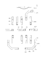
- the tray terminal 151 is a member formed by subjecting a conductive metal plate to punching, bending, etc., and includes a main body 153, a first contact portion 152 connected to one end of the main body 153, The second contact portion 154 is connected to the other end of the body portion 153.
- the main body portion 153 includes a bent portion 153a bent in a crank shape in a side view, and is held by the terminal holding portion 177a in a state where at least a part thereof is embedded in the terminal holding portion 177a.
- the first contact portion 152 is a flat plate-shaped portion connected to the lower end of the bent portion 153a, and the lower surface thereof is the lower surface of the bottom wall portion 177 (in the example shown in the figure, the terminal holding portion 177a). Is exposed and fixed to the connector 1, and contacts the connector terminal 51 of the connector 1 to be electrically conductive. As shown in the figure, it is desirable that the lower surface of the first contact portion 152 and the lower surface of the bottom wall portion 177 be substantially flush with each other, that is, flush with each other. Accordingly, when the tray 170 is inserted into the connector 1, the tray 170 can be smoothly inserted into the connector 1 without being caught by the connector 1.
- the lower surface of the first contact portion 152 is not necessarily located on substantially the same plane as the lower surface of the bottom wall portion 177 as long as at least a part thereof is exposed to the lower surface of the bottom wall portion 177. Good. That is, as long as the amount of protrusion of the lower surface of the first contact portion 152 and the lower surface of the bottom wall portion 177 with respect to the other does not reduce the work efficiency when the tray 170 is inserted into the connector 1, the first contact portion.
- the lower surface of 152 and the lower surface of the bottom wall portion 177 do not have to be located on the same plane.
- the first contact portion 152 is not elastically deformable in the example shown in the drawing, it may be formed in a shape that is elastically deformable.
- the second contact portion 154 has a substantially S-shaped shape in a side view, and is connected to the first bending portion 154a and the second bending portion 154b, which are each bent about 180 degrees, and the second bending portion 154b. It has a contact portion 154c that functions as a contact which is a tip portion and contacts the electrode pad 121 on the lower surface of the card 101 to be electrically conductive. Further, the range from the connecting portion of the second contact portion 154 with the main body portion 153 to the contact portion 154c is the elastically deformable portion 154d that includes the first bending portion 154a and the second bending portion 154b.
- the elastic deformation portion 154d elastically deforms, and the contact portion 154c and the electrode.
- the pad 121 can be elastically contacted.
- the elastically deforming portion 154d is located in the tray terminal accommodating recess 178 of the bottom wall portion 177, and does not come into contact with other members or parts even when elastically deforming. Therefore, an excessive elastic force is not applied to the electrode pad 121 of the card 101, and the electrode pad 121 is neither damaged nor damaged.
- the connector 1 includes a housing 11 having a recess 12 for accommodating a tray 170, a connector cover 61 for covering the housing 11, a connector terminal 51 connectable to the tray terminal 151, and a connector 1 inserted into the connector 1. And a discharge mechanism 20 for discharging the separated tray 170.
- the housing 11 is an integrally molded member made of an insulating material, and has a bottom wall portion 11b serving as a substantially rectangular flat plate-shaped terminal holding portion, and an insertion direction of the tray 170 in the housing 11 (X-axis direction). It extends in the width direction along the front front end, extends in the insertion direction along the inner wall 11a which is thicker than the bottom wall 11b, and the left and right side edges of the housing 11, and extends more than the bottom wall 11b. It includes a pair of thick side wall portions 11d and a push rod holding portion 11g integrally formed with one side wall portion 11d (on the right side in the insertion direction of the tray 170 in the example shown in the drawing).
- a push rod housing groove 11h extending in the insertion direction is formed in the push rod holding portion 11g.
- the other side wall portion 11d (in the example shown in the drawing, the left side in the insertion direction of the tray 170) may be provided with a holding portion 75 for preventing the tray 170 housed in the recess 12 from falling or dropping.
- the holding portion 75 is a region that can be elastically deformed, and a part of the holding portion 75 projects into the concave portion 12 that is the accommodation space, and biases the side surface of the accommodated tray 170 to retain the tray 170. Has become.
- the holding portion 75 is not limited to such a structure, and may have any structure as long as the tray 170 is held in the recess 12 without dropping or dropping. .. Further, when the tray 170 is held in the recess 12 by another means such as elasticity of the connector terminal 51, the holding portion 75 may not be provided.
- the lower surface of the inner wall portion 11a, the side wall portion 11d, and the push rod holding portion 11g are flush with the lower surface of the bottom wall portion 11b, and the upper surface thereof is located above the upper surface of the bottom wall portion 11b.
- the front end face of the housing 11 in the insertion direction is referred to as a front end face 11f
- the rear end face in the insertion direction is referred to as a rear end face 11r.
- a plurality of connector terminal accommodating recesses 11k are formed in the bottom wall 11b, and one connector terminal 51 is accommodated in each connector terminal accommodating recess 11k.
- the connector terminal accommodating recess 11k does not necessarily have to be a through hole, but here, it will be described as a through hole that penetrates the bottom wall portion 11b in the plate thickness direction or in the vertical direction (Z-axis direction). Further, the connector terminals 51 do not necessarily have to be housed in all the connector terminal housing recesses 11k.
- the connector terminal accommodating recess 11k and the connector terminal 51 are disposed so as to correspond to the disposition of the first contact portion 152 of the tray terminal 151 exposed on the lower surface of the bottom wall portion 177 of the tray 170 accommodated in the recess 12,
- the plurality of connector terminals 51 are arranged so that two rows are formed in the front and rear in the width direction.
- a terminal support portion 11j that supports the tip portion 55 of the connector terminal 51 is disposed in each connector terminal housing recess 11k.
- the terminal support portion 11j is arranged at one end in the longitudinal direction within the connector terminal accommodating recess 11k.
- the connector terminal 51 is a member formed by subjecting a metal plate to stamping, bending, etc., and includes a main body portion 53, a connecting portion 52 connected to one end of the main body portion 53, and the main body portion 53. A contact portion 54 connected to the other end and a tip portion 55 connected to the tip of the contact portion 54 are provided.
- the connector terminal 51 is preferably integrated with the housing 11 by a molding method such as insert molding (overmolding).
- the main body portion 53 includes a bent portion 53a bent in a crank shape in a side view, and is held by the bottom wall portion 11b in a state where at least a part thereof is embedded in the bottom wall portion 11b.
- connection portion 52 is a flat plate-shaped portion connected to the lower end of the bent portion 53a, the lower surface of which is exposed on the lower surface of the bottom wall portion 11b and the upper surface of the circuit board of the electronic device. Are connected by a connecting means such as soldering so that they can be electrically conducted.
- the lower surface of the connecting portion 52 and the lower surface of the bottom wall portion 11b are substantially flush with each other, that is, they are flush with each other.
- the lower surface of the wall portion 11b does not necessarily have to be located on substantially the same plane, and for example, the lower surface of the connecting portion 52 may be located below the lower surface of the bottom wall portion 11b.
- the contact portion 54 has a curved shape so as to bulge upward in a side view, and is elastically deformable.
- the top portion of the contact portion 54 is located above the upper surface of the bottom wall portion 11b, and the first contact of the tray terminal 151 exposed on the lower surface of the bottom wall portion 177 of the tray 170 housed in the recess 12. It is possible to contact the portion 152.
- the contact portion 54 is elastically deformed when pressed by the first contact portion 152 of the tray terminal 151, and thus can elastically contact the first contact portion 152. Further, the contact portion 54 is located in the connector terminal accommodating concave portion 11k, and does not come into contact with other members or parts even when elastically deformed.
- the tip portion 55 connected to the tip of the contact portion 54 has a flat plate shape, the lower surface of which is in contact with the upper surface of the terminal supporting portion 11j and is supported by the terminal supporting portion 11j from below.
- the contact portion 54 functions as a leaf spring supported at both ends in the longitudinal direction, so that the elastic force thereof is improved and the contact state with the first contact portion 152 is stably maintained. Note that, for example, when the elastic force of the contact portion 54 is sufficiently large, the lower surface of the tip portion 55 does not necessarily have to abut the upper surface of the terminal support portion 11j.
- the discharging mechanism 20 includes an eject lever 21 as a discharging lever member and a push rod 22 as a discharging operation member.
- the push rod 22 is a substantially linear rod-shaped or strip-shaped member, and is attached to the push rod holding groove 11h of the push rod holding portion 11g so as to be slidable in the front-rear direction (the insertion direction and the discharge direction of the tray 170). ing.
- a bent operation portion 22a is integrally connected to the rear end portion of the push rod 22.
- An engaging portion 22b that engages with the force applying portion 21b of the eject lever 21 is formed at the front end portion of the push rod 22.
- the eject lever 21 is pivotally attached to a support shaft 11c formed on the back wall 11a at a fulcrum 21c thereof.
- the end of the eject lever 21 on the opposite side of the force point portion 21b with the fulcrum portion 21c interposed therebetween comes into contact with the front end surface 171f of the tray housing 171 of the tray 170 housed in the recess 12 and is discharged to the tray 170 in the discharging direction. Functioning as an action point portion 21a that applies the force. Therefore, when a forward pressing force is applied to the operation portion 22a from the operation member inserted through the operation insertion hole 172b, the forward pressing force is applied from the push rod 22 to the force point portion 21b. As a result, the force is applied from the point of action 21a to the tray housing 171 in the ejection direction, and the tray 170 is ejected rearward from the recess 12.
- the connector cover 61 is a member that covers the upper surface of the housing 11, and is preferably a member that is formed by subjecting a conductive metal plate to stamping, bending, and the like, and includes a flat plate-shaped top plate portion 62.
- the top plate portion 62 has a front plate portion 63a standing upright from a front end edge thereof, and a side plate portion 63b standing upright from a pair of left and right side end edges of the top plate portion 62. Then, when the connector cover 61 is attached to the housing 11, the top plate portion 62 extends parallel to the bottom wall portion 11b and covers the upper portion of the recess 12, and the periphery of the recess 12 and the top plate portion 62 is covered.
- the defined space is formed as a storage space for storing the tray 170.
- the front plate portion 63a covers the outer surface of the front end surface 11f of the housing 11
- the side plate portion 63b covers the outer surface of the side wall portion 11d
- the lower end of the front plate portion 63a is soldered to the connection pad exposed on the upper surface of the circuit board of the electronic device. It is connected by connecting means such as attachment. Since the outside of the rear end surface 11r of the housing 11 is open without being covered by the connector cover 61, the rear end surface of the connector 1 becomes an opening and functions as an insertion port for the tray 170.
- the connector cover 61 does not have to be made of metal, but in that case, the connector cover 61 cannot be expected to have an effect of suppressing noise generated from the card 101, the electronic device, or the like.
- the connector 1 is mounted on the circuit board by electrically connecting the connecting portion 52 of the connector terminal 51 to the connecting pad of the circuit board of the electronic device by connecting means such as soldering.
- the operator accommodates the card 101 in the recess 176 according to the shape of the recess 176 of the tray 170. Specifically, as shown in FIG. 6A, the attitude of the card 101 is controlled so that the cutout portion 101c of the card 101 corresponds to the polarity-imparting convex portion 176c of the concave portion 176, and the inside of the concave portion 176 is controlled. Place it. As a result, the card 101 is accommodated in the recess 176 in an appropriate posture, that is, the lower surface thereof faces the bottom wall portion 177 and the electrode pads 121 on the lower surface correspond to the corresponding tray terminals 151.
- the card 101 is urged against the frame portion 173 of the housing 171 of the tray 170, so that the card 101 does not drop or drop from the concave portion 176. Further, in this state, the electrode pad 121 on the lower surface of the card 101 does not receive the elastic force from the tray terminal 151, and contacts the second contact portion 154 of the tray terminal 151 with a force about the weight of the card 101. It is in a state of being.
- the operator moves the tray 170 in the insertion direction toward the insertion opening of the tray 170 formed by the housing 11 of the connector 1 and the connector cover 61, and moves the tray 170 in a predetermined space in the accommodation space of the connector 1. Insert to position and complete insertion.
- the elastic force of the tray terminal 151 acts on the electrode pad 121 of the card 101. That is, since the upper surface of the card 101 (the surface on which the electrode pads 121 are not formed) is prevented from moving upward due to at least a portion of the top plate portion 62 of the connector cover 61 contacting the tray terminal 151, Therefore, the elastic force can be surely applied to the electrode pad 121 of the card 101. More specifically, as shown in FIG.
- the elastically deforming portion 154d of the second contact portion 154 of the tray terminal 151 is elastically deformed, and the elastic force generated thereby elastically deforms the contact portion 154c of the second contact portion 154.
- the second contact portion 154 has a substantially S-shape when viewed from the side and has a sufficient spring length, so that the elastically movable range of the contact portion 154c located at the free end thereof is sufficient. It is possible to exert a large and sufficiently large elastic force.
- the connector terminal 51 is securely connected to the first contact portion 152 of the tray terminal 151.
- Elastic force can be added. More specifically, as shown in FIG. 7, the contact portion 54 of the connector terminal 51 is elastically deformed, and due to the elastic force generated by this, the top portion of the contact portion 54 that is curved so as to bulge upward. Is pressed by the first contact portion 152 of the tray terminal 151. Since the contact portion 54 functions as a leaf spring supported at both ends in the longitudinal direction, the elastically movable range of the top portion can be sufficiently large and a sufficiently large elastic force can be exerted.
- the tray terminals 151 and the connector terminals 51 are connected in a state in which the elastic forces exerted by the tray terminals 151 and the connector terminals 51 are applied, the electrode pads 121 of the card 101 and the connection pads of the circuit board are in the card connector set. Through the tray 170 and the connector 1, the electric connection is made reliably and stably.
- an operator inserts a thin rod-shaped operation member (not shown) such as a pin or a rod from the rear of the tray 170 into the operation insertion hole 172b formed in the flange portion 172a of the tray housing 171 to insert the operation member.
- the tip is brought into contact with the operating portion 22a of the push rod 22.
- the force point portion 21b of the eject lever 21 engaging with the engaging portion 22b of the push rod 22 is displaced forward. Therefore, the front end surface 171f of the tray housing 171 is pushed by the action point portion 21a of the eject lever 21, and the tray 170 is displaced from the predetermined position toward the rear end surface 11r of the housing 51 (discharging direction).
- the holding portion 75 urges the side surface of the tray 170 to hold the tray 170, but it is considered that the force with which the operator pushes the push rod 22 through the operating member is sufficiently large.
- the holding of the tray 170 by the holding portion 75 is easily released, and the tray 170 moves toward the rear end surface 11r of the housing 51 and is ejected from the connector 1. Then, the operator can easily take out the ejected tray 170 from the connector 1.
- the ejecting mechanism 20 is not limited to this embodiment, and may be a known mechanism such as a push-push method or a method of picking up and pulling out the tray 170 with fingers, and is a mechanism capable of ejecting the tray 170. If it is, it may be anything.
- the card 101 and the circuit board (not shown) can be electrically connected in a state where the card 101 is accommodated in the tray 170. Therefore, the electrode pad 121 of the card 101 can be electrically connected to the connector terminal 51 without sliding on the connector terminal 51, and the electrode pad 121 of the card 101 can be prevented from being damaged or damaged. You can
- the tray 170 has the two recesses 12, that is, the accommodation spaces for the two cards 101.
- the number of the recesses 12 may be one or three or more, and may be any number.
- the plurality of tray terminals 151 or the plurality of connector terminals 51 are arranged on the bottom wall portion 177 of the tray housing 171 or the bottom wall portion 11b of the housing 11 so as to form two rows.
- the number of rows of 151 or connector terminals 51 may be one row or three or more rows, and may be any number.
- the tray terminals 151 or the connector terminals 51 held on the first and second rows of the tray terminals 151 or the connector terminals 51 are arranged so that the orientations thereof are opposite to the insertion and ejection directions (front and rear directions). However, they may be arranged in the same direction, or may be arranged in any direction.
- the tray 170 can hold the card 101 having the electrode pad 121 and can be inserted into the connector 1 having the connector terminal 51.
- the tray 170 includes a tray housing 171 that includes a recess 176 that can accommodate the card 101, a bottom wall 177 that defines the bottom of the recess 176, and a tray terminal storage recess 178 that is formed in the bottom wall 177.
- the second contact portion 154 includes a tray terminal 151 including a first contact portion 152 that can contact the connector terminal 51 and a second contact portion 154 that can contact the electrode pad 121.
- the tray terminal accommodating recess 178 is fixed and exposed on the surface of the bottom wall portion 177 opposite to the bottom surface of the recess 176, and the second contact portion 154 has at least the contact portion 154c protruding from the bottom surface of the recess 176. It is accommodated inside so as to be elastically deformable.
- the card connector set is a connector including a tray 170 and a connector 1 into which the tray 170 can be inserted, the connector terminal 51 including a contact portion 54 that is elastically deformable and that can contact the first contact portion 152. 1 and.
- the first contact portion 152 that can contact the connector terminal 51 of the connector 1 is fixed, and only the second contact portion 154 that can contact the electrode pad 121 of the card 101.
- the thickness (vertical dimension) of the tray housing 171 can be suppressed even if the elastic deformation range of the second contact portion 154 is increased, and the tray 170 is small and thin.
- the entire card connector set can be made smaller and thinner, and moreover, it is possible to deal with the card 101 having a large number of electrodes and a large number of electrode pads 121.
- the second contact portion 154 can be elastically deformed in the tray terminal accommodating recess 178 without interfering with other members.
- the tray terminal 151 is arranged so that, in a plan view, the second contact portion 154 forms a single row or a plurality of rows arranged along the width direction orthogonal to the insertion direction of the tray 170.
- the tray terminal 151 is arranged such that the main body 153 extends in the insertion direction of the tray 170 in a plan view.
- each of the connector terminals 51 extends in the insertion direction of the tray 170, and the contact portion 54 has one or a plurality of rows arranged in a width direction orthogonal to the insertion direction of the tray 170 in a plan view. Are arranged to form.
- FIG. 8 is a perspective view showing a state in which a connector cover of a card connector set in which a tray not holding a card is inserted into a connector in the second embodiment is removed
- FIG. 9 is a bottom view of the card in the second embodiment.
- FIG. 10 is an exploded view of the tray in the second embodiment
- FIG. 11 is a top view showing the arrangement of the tray terminals in the second embodiment
- FIG. 12 is the tray inserted into the connector in the second embodiment.
- FIG. 3 is a two-sided view of the card connector set in which the connector cover is removed. Note that, in FIG.
- (a) is a top view of a state in which the card is not held
- (b) is a cross-sectional view taken along the line BB in (a), showing the state of holding the card
- (C) is a sectional view taken along the line CC in (a), showing a state in which the card is held.
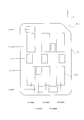
- the electrode pads 121 of the card 101 include a plurality of types of shapes and sizes, and form a plurality of rows and a plurality of columns in a plan view. It is located in.
- the electrode pad 121 has five rows of first to fifth rows (Line1 to 5) and five columns of first to fifth columns (Column1 to 5). Constitute.
- the electrode pads 121 do not necessarily exist in the positions corresponding to all the columns in each row, and do not necessarily exist in the positions corresponding to all the rows in each column. ..
- the electrode pads 121 are not necessarily arranged so as to correspond to all the components of the matrix made up of the first to fifth rows and the first to fifth columns.
- the electrode pad 121 existing at the position corresponding to the component (i, j) in the j-th column in the i-th row will be referred to as an electrode pad 121(i, j).
- the card 101 is a nano-SIM card (nSIM card) or the like that is small and thin and has multiple poles, a large number of electrode pads 121 of the same shape and size are densely arranged and a small number of about 1 to 2 rows. It is difficult to arrange the lower surface of the card 101 so as to form a row, and as in the example shown in FIG. 9, the electrode pads 121 having a plurality of shapes and sizes are arranged in a matrix of many rows and many columns. It only needs to be placed in locations that correspond to some of the selected.
- nSIM card nano-SIM card
- the arrangement of the connection pads exposed on the upper surface of the circuit board of the electronic device is the same as that of the first embodiment because of the wiring of the circuit board, and accordingly, the corresponding arrangement is provided.
- the arrangement of the connector terminals 51 is also the same as in the first embodiment. That is, in this embodiment, the structure of the connector 1 is the same as that of the first embodiment, and therefore the description thereof is omitted.
- the tray 170 in the present embodiment is the same as the first embodiment except for the tray terminal accommodating recess 178 formed in the bottom wall portion 177 of the tray housing 171 and the tray terminal 151 accommodated in the tray terminal accommodating recess 178.
- the configuration of the tray 170 other than the tray terminal accommodating concave portion 178 and the tray terminal 151 is omitted because it is similar to that of the first embodiment.
- the tray terminal accommodating recesses 178 in the present embodiment are arranged so as to form five rows and five columns, but in each row, not all columns are necessarily arranged. It does not exist at the corresponding position, and does not necessarily exist at the position corresponding to all rows in each column.
- the tray terminal accommodating recessed portion 178 is arranged in a component corresponding to the electrode pad 121, although not all of the components of the matrix including the first to fifth rows and the first to fifth columns. ..
- the tray terminal 151 in the present embodiment is arranged such that the second contact portion 154 thereof constitutes five rows and five columns, like the electrode pad 121 of the card 101. It does not necessarily exist in the position corresponding to all the columns in each row, and does not necessarily exist in the position corresponding to all the rows in each column.
- the second contact portion 154 of the tray terminal 151 does not necessarily include all the components of the matrix including the first to fifth rows and the first to fifth columns, but the components corresponding to the electrode pads 121 include: It is arranged.
- Each of the second contact portions 154 of the tray terminals 151 is housed in the corresponding tray terminal housing recess 178.
- the tray terminal 151 in the present embodiment includes a first type tray terminal 151A and a second type tray terminal 151B.
- the first type tray terminal 151A has the same configuration as the tray terminal 151 in the first embodiment, but its posture is the same as the tray terminal 151 in the first embodiment in the front-back direction.
- the column-direction tray terminals 151A1 arranged to be controlled so as to extend in the insertion and ejection direction of the tray 170, that is, the X-axis direction, and the posture thereof in the left-right direction (the width direction of the tray 170, that is, the Y-axis).
- Directional) and row-direction tray terminals 151A2 that are arranged to be controlled.
- the main body portion 153 connecting the first contact portion 152 contacting the connector terminal 51 and the second contact portion 154 contacting the electrode pad 121 in the plan view has a front-back direction (column direction of the matrix). ) Is arranged so as to extend. Therefore, the row-direction tray terminal 151A1 electrically connects the connector terminal 51 and the electrode pad 121, which are located along the straight line extending in the front-rear direction in plan view, with the tray 170 inserted in the connector 1.
- the row direction tray terminal 151A2 electrically connects the connector terminal 51 and the electrode pad 121, which are located along a straight line extending in the left-right direction in a plan view, with the tray 170 inserted in the connector 1.
- the main body portion 153 of the second type tray terminal 151B extends linearly in a plan view like the main body portion 153 of the tray terminal 151 and the first type tray terminal 151A in the first embodiment. However, it includes a portion extending in the front-rear direction and a portion extending in the left-right direction. Specifically, the main body 153 of the second type tray terminal 151B includes a column direction portion 153d extending in the front-rear direction and a row direction portion 153b extending in the left-right direction.
- the column-direction portion 153d is connected to the first contact portion 152 and the row-direction portion 153b is connected to the second contact portion 154, but the column-direction portion 153d is the second contact portion.
- the row-direction portion 153b may be connected to the first contact portion 152.
- the column direction portion 153d and the row direction portion 153b are connected by an inclined direction portion 153c extending in a direction intersecting the front-rear direction and the left-right direction. If necessary, the column direction portion 153d and the row direction portion 153b may be directly connected, and the tilt direction portion 153c may be omitted.
- the second type tray terminal 151B includes the column direction portion 153d and the row direction portion 153b, when the tray 170 is inserted into the connector 1, with respect to the front-back direction and the left-right direction in a plan view. , The connector terminal 51 and the electrode pad 121 at different positions are electrically connected.
- the holding portion 161 in the present embodiment is a member integrally formed by subjecting a metal plate to punching, bending, or the like similarly to the tray terminal 151.
- the present invention is not limited to this, and it is a member that is elastically deformable, and a part of it projects into the recess 176 that is the accommodation space and biases the side surface of the accommodated card 101 to It may be of any type as long as it can hold 101.
- the tray terminal 151 includes the column-direction tray terminal 151A1 in which the main body portion 153 is arranged to extend in the insertion direction of the tray 170 and the main body portion 153 in plan view. Includes a row-direction tray terminal 151A2 arranged so as to extend in the width direction orthogonal to the insertion direction of the tray 170. Further, at least one tray terminal 151 includes a column direction portion 153d in which the main body 153 extends in the insertion direction of the tray 170, and the main body 153 is orthogonal to the insertion direction of the tray 170 in plan view. And a row-direction portion 153b arranged so as to extend in the width direction. Further, the tray terminal 151 further includes an inclined direction portion 153c connecting the column direction portion 153d and the row direction portion 153b.
- the card 101 in which the electrode pads 121 having a plurality of shapes and sizes are arranged only at the positions corresponding to some selected from the components in the matrix of many rows and many columns. ..
- the present disclosure can be applied to a card holding member and a card connector set.
Landscapes
- Engineering & Computer Science (AREA)
- Physics & Mathematics (AREA)
- General Physics & Mathematics (AREA)
- Theoretical Computer Science (AREA)
- Artificial Intelligence (AREA)
- Computer Vision & Pattern Recognition (AREA)
- Computer Hardware Design (AREA)
- Microelectronics & Electronic Packaging (AREA)
- Coupling Device And Connection With Printed Circuit (AREA)
Abstract
La présente invention peut être utilisée pour une carte qui est de taille réduite et amincie, a de multiples pôles, peut assurer une miniaturisation, un profil bas et de multiples pôles, et permet d'obtenir une fiabilité améliorée. A cet effet, la présente invention comprend : un boîtier de plateau ayant une partie évidée dans laquelle la carte peut être logée, une partie de paroi inférieure qui définit la surface inférieure de la partie évidée, et une partie évidée de réception de borne de plateau formée dans la partie de paroi inférieure; et une borne de plateau qui est disposée sur la partie de paroi inférieure, et comprend une partie de corps principal dont au moins une partie est maintenue par la partie de paroi inférieure, une première partie de contact capable de venir en contact avec une borne de connecteur, et une seconde partie de contact capable de venir en contact avec une pastille d'électrode, la première partie de contact et la seconde partie de contact étant reliées aux deux extrémités de la partie de corps principal, respectivement, la première partie de contact étant fixe et exposée sur une surface de la partie de paroi inférieure opposée à la surface inférieure de la partie évidée, et la seconde partie de contact est logée dans la partie évidée de réception de borne de plateau d'une manière élastiquement déformable dans un état dans lequel au moins un point de contact entre celles-ci fait saillie à partir de la surface inférieure de la partie évidée.
Priority Applications (3)
| Application Number | Priority Date | Filing Date | Title |
|---|---|---|---|
| JP2021501839A JPWO2020170822A1 (ja) | 2019-02-20 | 2020-02-05 | カード保持部材及びカード用コネクタセット |
| CN202080014940.XA CN113439366A (zh) | 2019-02-20 | 2020-02-05 | 卡保持元件以及卡用连接器装置 |
| US17/429,956 US20220140510A1 (en) | 2019-02-20 | 2020-02-05 | Card retaining member and card connector set |
Applications Claiming Priority (2)
| Application Number | Priority Date | Filing Date | Title |
|---|---|---|---|
| US201962807804P | 2019-02-20 | 2019-02-20 | |
| US62/807,804 | 2019-02-20 |
Publications (1)
| Publication Number | Publication Date |
|---|---|
| WO2020170822A1 true WO2020170822A1 (fr) | 2020-08-27 |
Family
ID=72144453
Family Applications (1)
| Application Number | Title | Priority Date | Filing Date |
|---|---|---|---|
| PCT/JP2020/004357 Ceased WO2020170822A1 (fr) | 2019-02-20 | 2020-02-05 | Élément de support de carte et ensemble connecteur pour carte |
Country Status (4)
| Country | Link |
|---|---|
| US (1) | US20220140510A1 (fr) |
| JP (1) | JPWO2020170822A1 (fr) |
| CN (1) | CN113439366A (fr) |
| WO (1) | WO2020170822A1 (fr) |
Families Citing this family (2)
| Publication number | Priority date | Publication date | Assignee | Title |
|---|---|---|---|---|
| CN118171678B (zh) * | 2018-02-01 | 2025-05-23 | 华为技术有限公司 | 存储卡和终端 |
| TWM602292U (zh) * | 2020-07-03 | 2020-10-01 | 正崴精密工業股份有限公司 | Sim卡連接器 |
Citations (5)
| Publication number | Priority date | Publication date | Assignee | Title |
|---|---|---|---|---|
| JP3110835U (ja) * | 2005-04-01 | 2005-06-30 | 詮欣股▲分▼有限公司 | 標準sdメモリカード変換装置の構造 |
| US20060079133A1 (en) * | 2004-10-12 | 2006-04-13 | Samsung Electronics Co., Ltd. | Socket for trans-flash memory card |
| JP2006236261A (ja) * | 2005-02-28 | 2006-09-07 | Renesas Technology Corp | メモリカード用アダプタおよびメモリカード |
| CN2906997Y (zh) * | 2006-05-25 | 2007-05-30 | 黄进华 | 二合一储存卡适配器 |
| WO2008038428A1 (fr) * | 2006-09-27 | 2008-04-03 | Renesas Technology Corp. | Carte à circuit intégré et son étui |
Family Cites Families (10)
| Publication number | Priority date | Publication date | Assignee | Title |
|---|---|---|---|---|
| DE102004054150B4 (de) * | 2004-11-08 | 2007-11-29 | Lumberg Connect Gmbh | Kontaktiervorrichtung für eine Chipkarte, insbesondere für eine SIM- oder USIM-Karte |
| CN102231767B (zh) * | 2009-12-25 | 2013-12-25 | 深圳富泰宏精密工业有限公司 | 便携式电子装置及其芯片卡卡持装置 |
| CN103311721B (zh) * | 2012-03-16 | 2015-10-21 | 莫仕连接器(成都)有限公司 | 双sim卡托盘、连接器模块及电连接器装置 |
| JP6230242B2 (ja) * | 2013-03-01 | 2017-11-15 | モレックス エルエルシー | カード用コネクタ |
| US9761971B2 (en) * | 2014-06-06 | 2017-09-12 | Molex, Llc | Card holding member and card connector, which prevents short-circuits, prevents damage and wear, enables easier handling, and improves reliability |
| JP6457885B2 (ja) * | 2015-05-19 | 2019-01-23 | モレックス エルエルシー | カード用コネクタ |
| CN205335464U (zh) * | 2015-12-15 | 2016-06-22 | 阿尔卑斯电气株式会社 | 卡用连接器 |
| JP2018190589A (ja) * | 2017-05-02 | 2018-11-29 | Smk株式会社 | カードコネクタ |
| CN107093820B (zh) * | 2017-05-23 | 2024-01-05 | 广东杰思通讯股份有限公司 | 一种卡托及具有该卡托的移动终端 |
| US20190272453A1 (en) * | 2018-03-01 | 2019-09-05 | Apple Inc. | Dual sim card connector |
-
2020
- 2020-02-05 US US17/429,956 patent/US20220140510A1/en not_active Abandoned
- 2020-02-05 WO PCT/JP2020/004357 patent/WO2020170822A1/fr not_active Ceased
- 2020-02-05 CN CN202080014940.XA patent/CN113439366A/zh active Pending
- 2020-02-05 JP JP2021501839A patent/JPWO2020170822A1/ja active Pending
Patent Citations (5)
| Publication number | Priority date | Publication date | Assignee | Title |
|---|---|---|---|---|
| US20060079133A1 (en) * | 2004-10-12 | 2006-04-13 | Samsung Electronics Co., Ltd. | Socket for trans-flash memory card |
| JP2006236261A (ja) * | 2005-02-28 | 2006-09-07 | Renesas Technology Corp | メモリカード用アダプタおよびメモリカード |
| JP3110835U (ja) * | 2005-04-01 | 2005-06-30 | 詮欣股▲分▼有限公司 | 標準sdメモリカード変換装置の構造 |
| CN2906997Y (zh) * | 2006-05-25 | 2007-05-30 | 黄进华 | 二合一储存卡适配器 |
| WO2008038428A1 (fr) * | 2006-09-27 | 2008-04-03 | Renesas Technology Corp. | Carte à circuit intégré et son étui |
Also Published As
| Publication number | Publication date |
|---|---|
| JPWO2020170822A1 (ja) | 2021-11-25 |
| CN113439366A (zh) | 2021-09-24 |
| US20220140510A1 (en) | 2022-05-05 |
Similar Documents
| Publication | Publication Date | Title |
|---|---|---|
| CN108539478B (zh) | 卡保持元件及卡用连接器 | |
| JP5818366B2 (ja) | カード用コネクタ | |
| US9124042B2 (en) | Holder connected to an operation member via an elastic member | |
| JP6457885B2 (ja) | カード用コネクタ | |
| JP5738689B2 (ja) | カード用コネクタ | |
| KR100404629B1 (ko) | 카드 커넥터 | |
| CN101030684B (zh) | 卡连接器 | |
| CN205376818U (zh) | 卡固持元件及卡用连接器 | |
| JP2001357931A (ja) | カードコネクタ | |
| CN104466467A (zh) | 卡连接器 | |
| US20160028172A1 (en) | Card retention member and card connector | |
| US6839431B2 (en) | Card connector | |
| JP2012119070A (ja) | カード用コネクタ | |
| KR20080066761A (ko) | 카드 커넥터 | |
| WO2020170822A1 (fr) | Élément de support de carte et ensemble connecteur pour carte | |
| JP2019016603A (ja) | カード用コネクタ | |
| JP2006164749A (ja) | カードコネクタ | |
| JP4535710B2 (ja) | カード固定装置及びこれを用いた携帯端末機 | |
| CN102007498A (zh) | 卡连接器 | |
| JP6295165B2 (ja) | 端子ユニット及びカード用コネクタ | |
| JP2008084624A (ja) | カードコネクタ | |
| JP5986255B1 (ja) | カード保持部材及びカード用コネクタ | |
| JP4489643B2 (ja) | カード用コネクタ | |
| CN100364176C (zh) | 卡片插座 | |
| JP2017045678A (ja) | カード用コネクタ |
Legal Events
| Date | Code | Title | Description |
|---|---|---|---|
| 121 | Ep: the epo has been informed by wipo that ep was designated in this application |
Ref document number: 20759312 Country of ref document: EP Kind code of ref document: A1 |
|
| ENP | Entry into the national phase |
Ref document number: 2021501839 Country of ref document: JP Kind code of ref document: A |
|
| NENP | Non-entry into the national phase |
Ref country code: DE |
|
| 122 | Ep: pct application non-entry in european phase |
Ref document number: 20759312 Country of ref document: EP Kind code of ref document: A1 |