WO2020171050A1 - Dispositif à ondes élastiques - Google Patents
Dispositif à ondes élastiques Download PDFInfo
- Publication number
- WO2020171050A1 WO2020171050A1 PCT/JP2020/006215 JP2020006215W WO2020171050A1 WO 2020171050 A1 WO2020171050 A1 WO 2020171050A1 JP 2020006215 W JP2020006215 W JP 2020006215W WO 2020171050 A1 WO2020171050 A1 WO 2020171050A1
- Authority
- WO
- WIPO (PCT)
- Prior art keywords
- region
- film
- sound velocity
- acoustic
- wave device
- Prior art date
- Legal status (The legal status is an assumption and is not a legal conclusion. Google has not performed a legal analysis and makes no representation as to the accuracy of the status listed.)
- Ceased
Links
Images







Classifications
-
- H—ELECTRICITY
- H03—ELECTRONIC CIRCUITRY
- H03H—IMPEDANCE NETWORKS, e.g. RESONANT CIRCUITS; RESONATORS
- H03H9/00—Networks comprising electromechanical or electro-acoustic elements; Electromechanical resonators
- H03H9/02—Details
- H03H9/125—Driving means, e.g. electrodes, coils
- H03H9/145—Driving means, e.g. electrodes, coils for networks using surface acoustic waves
-
- H—ELECTRICITY
- H03—ELECTRONIC CIRCUITRY
- H03H—IMPEDANCE NETWORKS, e.g. RESONANT CIRCUITS; RESONATORS
- H03H1/00—Constructional details of impedance networks whose electrical mode of operation is not specified or applicable to more than one type of network
-
- H—ELECTRICITY
- H03—ELECTRONIC CIRCUITRY
- H03H—IMPEDANCE NETWORKS, e.g. RESONANT CIRCUITS; RESONATORS
- H03H9/00—Networks comprising electromechanical or electro-acoustic elements; Electromechanical resonators
- H03H9/02—Details
- H03H9/125—Driving means, e.g. electrodes, coils
- H03H9/145—Driving means, e.g. electrodes, coils for networks using surface acoustic waves
- H03H9/14538—Formation
- H03H9/14541—Multilayer finger or busbar electrode
-
- H—ELECTRICITY
- H03—ELECTRONIC CIRCUITRY
- H03H—IMPEDANCE NETWORKS, e.g. RESONANT CIRCUITS; RESONATORS
- H03H9/00—Networks comprising electromechanical or electro-acoustic elements; Electromechanical resonators
- H03H9/0004—Impedance-matching networks
-
- H—ELECTRICITY
- H03—ELECTRONIC CIRCUITRY
- H03H—IMPEDANCE NETWORKS, e.g. RESONANT CIRCUITS; RESONATORS
- H03H9/00—Networks comprising electromechanical or electro-acoustic elements; Electromechanical resonators
- H03H9/02—Details
- H03H9/02007—Details of bulk acoustic wave devices
-
- H—ELECTRICITY
- H03—ELECTRONIC CIRCUITRY
- H03H—IMPEDANCE NETWORKS, e.g. RESONANT CIRCUITS; RESONATORS
- H03H9/00—Networks comprising electromechanical or electro-acoustic elements; Electromechanical resonators
- H03H9/02—Details
- H03H9/02535—Details of surface acoustic wave devices
- H03H9/02637—Details concerning reflective or coupling arrays
-
- H—ELECTRICITY
- H03—ELECTRONIC CIRCUITRY
- H03H—IMPEDANCE NETWORKS, e.g. RESONANT CIRCUITS; RESONATORS
- H03H9/00—Networks comprising electromechanical or electro-acoustic elements; Electromechanical resonators
- H03H9/02—Details
- H03H9/02535—Details of surface acoustic wave devices
- H03H9/02818—Means for compensation or elimination of undesirable effects
- H03H9/02858—Means for compensation or elimination of undesirable effects of wave front distortion
-
- H—ELECTRICITY
- H03—ELECTRONIC CIRCUITRY
- H03H—IMPEDANCE NETWORKS, e.g. RESONANT CIRCUITS; RESONATORS
- H03H9/00—Networks comprising electromechanical or electro-acoustic elements; Electromechanical resonators
- H03H9/02—Details
- H03H9/02535—Details of surface acoustic wave devices
- H03H9/02818—Means for compensation or elimination of undesirable effects
- H03H9/02881—Means for compensation or elimination of undesirable effects of diffraction of wave beam
-
- H—ELECTRICITY
- H03—ELECTRONIC CIRCUITRY
- H03H—IMPEDANCE NETWORKS, e.g. RESONANT CIRCUITS; RESONATORS
- H03H9/00—Networks comprising electromechanical or electro-acoustic elements; Electromechanical resonators
- H03H9/02—Details
- H03H9/02535—Details of surface acoustic wave devices
- H03H9/02992—Details of bus bars, contact pads or other electrical connections for finger electrodes
-
- H—ELECTRICITY
- H03—ELECTRONIC CIRCUITRY
- H03H—IMPEDANCE NETWORKS, e.g. RESONANT CIRCUITS; RESONATORS
- H03H9/00—Networks comprising electromechanical or electro-acoustic elements; Electromechanical resonators
- H03H9/02—Details
- H03H9/125—Driving means, e.g. electrodes, coils
- H03H9/145—Driving means, e.g. electrodes, coils for networks using surface acoustic waves
- H03H9/14544—Transducers of particular shape or position
- H03H9/1457—Transducers having different finger widths
-
- H—ELECTRICITY
- H03—ELECTRONIC CIRCUITRY
- H03H—IMPEDANCE NETWORKS, e.g. RESONANT CIRCUITS; RESONATORS
- H03H9/00—Networks comprising electromechanical or electro-acoustic elements; Electromechanical resonators
- H03H9/25—Constructional features of resonators using surface acoustic waves
-
- H—ELECTRICITY
- H03—ELECTRONIC CIRCUITRY
- H03H—IMPEDANCE NETWORKS, e.g. RESONANT CIRCUITS; RESONATORS
- H03H9/00—Networks comprising electromechanical or electro-acoustic elements; Electromechanical resonators
- H03H9/46—Filters
- H03H9/54—Filters comprising resonators of piezoelectric or electrostrictive material
-
- H—ELECTRICITY
- H03—ELECTRONIC CIRCUITRY
- H03H—IMPEDANCE NETWORKS, e.g. RESONANT CIRCUITS; RESONATORS
- H03H9/00—Networks comprising electromechanical or electro-acoustic elements; Electromechanical resonators
- H03H9/02—Details
- H03H9/02007—Details of bulk acoustic wave devices
- H03H9/02157—Dimensional parameters, e.g. ratio between two dimension parameters, length, width or thickness
-
- H—ELECTRICITY
- H03—ELECTRONIC CIRCUITRY
- H03H—IMPEDANCE NETWORKS, e.g. RESONANT CIRCUITS; RESONATORS
- H03H9/00—Networks comprising electromechanical or electro-acoustic elements; Electromechanical resonators
- H03H9/02—Details
- H03H9/02535—Details of surface acoustic wave devices
- H03H9/02543—Characteristics of substrate, e.g. cutting angles
- H03H9/02574—Characteristics of substrate, e.g. cutting angles of combined substrates, multilayered substrates, piezoelectrical layers on not-piezoelectrical substrate
Definitions
- the present invention relates to an acoustic wave device.
- Patent Document 1 discloses an example of an elastic wave device using a piston mode.
- This acoustic wave device has an edge region with a low sound velocity. More specifically, the edge regions are located at both ends in the extending direction of the electrode fingers in a region where adjacent electrode fingers of the IDT electrode (Inter Digital Transducer) overlap in the elastic wave propagation direction.
- the width of the electrode finger in the edge region is widened, or a dielectric film for adding mass is provided on the electrode finger in the edge region, so that the sound velocity in the edge region is reduced. This suppresses the transverse mode ripple.
- a piezoelectric substrate having a crystal axis inclined with respect to the thickness direction may be used.
- the displacement distribution in the extending direction of the electrode fingers is asymmetric. In such a case where the displacement distribution is asymmetric, it is difficult for the conventional acoustic wave device using the piston mode to sufficiently suppress the transverse mode.
- An object of the present invention is to provide an elastic wave device that can effectively suppress transverse modes.
- An elastic wave device includes a piezoelectric layer having a crystal axis and an IDT electrode provided on the piezoelectric layer, and the elastic wave propagation direction is a first direction, and the first direction is the first direction.
- the crystal axis of the piezoelectric layer is inclined in the second direction with respect to the thickness direction of the piezoelectric layer, and the IDT electrode, A first bus bar and a second bus bar facing each other, a plurality of first electrode fingers having one end connected to the first bus bar, and one end connected to the second bus bar, and A first electrode finger and a plurality of second electrode fingers that are interleaved with each other, and a portion where the first electrode finger and the second electrode finger overlap in the first direction is A crossover region, wherein the crossover region is located on the central side in the second direction and on the first busbar side of the central region, and A first low sound velocity region having a low sound velocity; and a second low sound velocity region having a sound
- the transverse mode can be effectively suppressed.
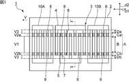
- FIG. 1 is a plan view of an elastic wave device according to a first embodiment of the present invention.
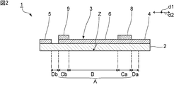
- FIG. 2 is a sectional view taken along the line II in FIG.
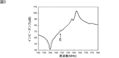
- FIG. 3 is a diagram showing impedance frequency characteristics of the first embodiment of the present invention and a comparative example.
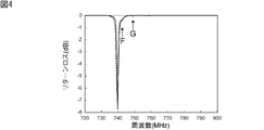
- FIG. 4 is a diagram showing the return loss of the first embodiment of the present invention and the comparative example.
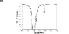
- FIG. 5 is an enlarged view of FIG.
- FIG. 6 is a plan view of an elastic wave device according to a first modification of the first embodiment of the present invention.
- FIG. 7 is a plan view showing the vicinity of a pair of electrode fingers of the IDT electrode in the second modified example of the first embodiment of the present invention.
- FIG. 1 is a plan view of an elastic wave device according to a first embodiment of the present invention.
- FIG. 2 is a sectional view taken along the line II in FIG.
- FIG. 3 is a diagram showing impedance frequency characteristics of the first embodiment of the present invention and a comparativ
- FIG. 8 is a sectional view of an elastic wave device according to a third modification of the first embodiment of the present invention.
- FIG. 9 is a plan view showing the vicinity of a pair of electrode fingers of the IDT electrode in the fourth modified example of the first embodiment of the present invention.
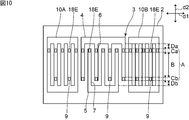
- FIG. 10 is a plan view of an elastic wave device according to a fifth modification of the first embodiment of the present invention.
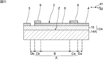
- FIG. 11 is a sectional view of an elastic wave device according to a sixth modification of the first embodiment of the present invention.
- FIG. 12 is a sectional view of an elastic wave device according to a seventh modified example of the first embodiment of the present invention.
- FIG. 13 is a cross-sectional view of an acoustic wave device according to an eighth modification of the first embodiment of the present invention.
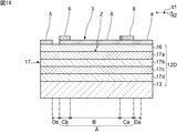
- FIG. 14 is a sectional view of an elastic wave device according to a ninth modification of the first embodiment of the present invention.
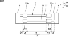
- FIG. 15 is a plan view showing the vicinity of a pair of electrode fingers of the IDT electrode according to the second embodiment of the present invention.
- FIG. 16 is a plan view showing the vicinity of a pair of electrode fingers of the IDT electrode according to the modification of the second embodiment of the present invention.
- FIG. 17 is a sectional view of an acoustic wave device according to a third embodiment of the present invention.
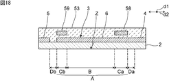
- FIG. 18 is a sectional view of an elastic wave device according to the fourth embodiment of the present invention.
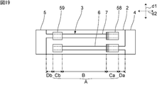
- FIG. 19 is a plan view showing the vicinity of a pair of electrode fingers of the IDT electrode according to the fourth embodiment of the present invention.
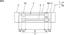
- FIG. 20 is a plan view showing the vicinity of a pair of electrode fingers of the IDT electrode in the first modified example of the fourth exemplary embodiment of the present invention.
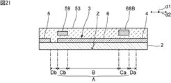
- FIG. 21 is a sectional view of an elastic wave device according to a second modification of the fourth embodiment of the present invention.
- FIG. 22 is a plan view of an elastic wave device according to the fifth embodiment of the present invention.
- FIG. 23 is a sectional view of an elastic wave device according to a fifth embodiment of the present invention.
- FIG. 1 is a plan view of an elastic wave device according to a first embodiment of the present invention.
- FIG. 2 is a sectional view taken along the line II in FIG.
- a part of the mass addition film described later may be shown by hatching.
- a part of the mass addition film may be shown by hatching different from other parts.
- the acoustic wave device 1 has a piezoelectric substrate 2.
- the piezoelectric substrate 2 of the present embodiment is a piezoelectric substrate composed of only a piezoelectric layer. More specifically, the piezoelectric substrate 2 is a piezoelectric single crystal substrate and has a crystal axis Z as shown in FIG.
- a piezoelectric single crystal such as lithium niobate or lithium tantalate can be used.
- the piezoelectric substrate 2 may be a laminated body including a piezoelectric layer. In this case, the piezoelectric layer may have the crystal axis Z.
- the IDT electrode 3 is provided on the piezoelectric substrate 2. By applying an AC voltage to the IDT electrode 3, elastic waves are excited. Reflectors 10A and 10B are provided on both sides of the IDT electrode 3 in the elastic wave propagation direction on the piezoelectric substrate 2.
- the elastic wave device 1 of the present embodiment is an elastic wave resonator.
- the elastic wave device 1 according to the present invention is not limited to the elastic wave resonator, and may be a filter device having a plurality of elastic wave resonators.
- the elastic wave propagation direction is defined as a first direction d1 and the direction orthogonal to the first direction d1 is defined as a second direction d2.
- the crystal axis Z of the piezoelectric substrate 2 is inclined in the second direction d2 with respect to the thickness direction of the piezoelectric substrate 2.
- the crystal axis Z may be tilted in the second direction d2, and may be tilted in the first direction d1 at the same time.
- the IDT electrode 3 has a first bus bar 4 and a second bus bar 5 facing each other.
- the IDT electrode 3 has a plurality of first electrode fingers 6 each having one end connected to the first bus bar 4.
- the IDT electrode 3 has a plurality of second electrode fingers 7 each having one end connected to the second bus bar 5.
- the plurality of first electrode fingers 6 and the plurality of second electrode fingers 7 are interleaved with each other.
- the IDT electrode 3, the reflector 10A, and the reflector 10B may be made of a laminated metal film in which a plurality of metal layers are laminated, or may be made of a single-layer metal film.
- the crossover area A has a central area B located on the central side in the second direction d2.
- the intersection area A includes a first edge area Ca arranged on the first bus bar 4 side of the central area B and a second edge area Cb arranged on the second bus bar 5 side of the central area B.
- the first edge region Ca the first mass addition film 8 is provided on each of the first electrode finger 6 and the second electrode finger 7.
- a first low sound speed area having a lower sound speed than the sound speed in the central area B is formed.
- the second mass addition film 9 is provided on each of the first electrode finger 6 and the second electrode finger 7.
- a second low sound velocity region having a lower sound velocity than the sound velocity in the central region B is formed.
- the first mass addition film 8 and the second mass addition film 9 are also provided on the reflector 10A and the reflector 10B.
- the position of the first mass addition film 8 on the reflector 10A and the reflector 10B is the same as the position of the first mass addition film 8 on the IDT electrode 3.
- the position of the second mass addition film 9 on the reflector 10A and the reflector 10B in the second direction d2 is the same as the position of the second mass addition film 9 on the IDT electrode 3.
- the first mass addition film 8 and the second mass addition film 9 may not be provided on the reflector 10A and the reflector 10B.
- first mass addition film 8 and the second mass addition film 9 As a material of the first mass addition film 8 and the second mass addition film 9, an appropriate metal or dielectric can be used. In this embodiment, the first mass addition film 8 and the second mass addition film 9 are made of the same material.
- the dimension of the first mass-adding film 8 along the second direction d2 is larger than the dimension of the second mass-adding film 9 along the second direction d2.
- a portion of the first mass-adding film 8 in which the dimensions of the first mass-adding membrane 8 are larger than that of the second mass-adding membrane 9 is indicated by hatching different from other portions. ..
- the configuration of the first low sound velocity region and the configuration of the second low sound velocity region are asymmetric.
- the sound velocity in the central region B is V1
- the sound velocity in the first low sound velocity region is V2a
- the sound velocity in the second low sound velocity region is V2b
- the first mass addition film 8 may be provided on one of the plurality of first electrode fingers 6 and the plurality of second electrode fingers 7. ..
- the second mass addition film 9 may be provided on one of the plurality of first electrode fingers 6 and the plurality of second electrode fingers 7. ..
- the IDT electrode 3 has a first outer area Da that is arranged outside the first edge area Ca in the second direction d2. Further, the IDT electrode 3 has a second outer region Db arranged outside the second edge region Cb in the second direction d2.
- the first edge area Ca is located between the central area B and the first outer area Da.
- the second edge area Cb is located between the central area B and the second outer area Db.
- the first outer area Da is located between the first edge area Ca and the first bus bar 4.
- the second outer region Db is located between the second edge region Cb and the second bus bar 5.
- the sound velocities in the first outer region Da and the second outer region Db are higher than the sound velocities in the central region B.
- the sound velocity of the elastic wave in the first outer region Da and the second outer region Db is V3, V1 ⁇ V3.
- the first high sound velocity region is formed in the first outer region Da
- the second high sound velocity region is formed in the second outer region Db.
- FIG. 1 shows the relationship between the sound velocities as described above.
- the sonic velocity is higher as the line indicating the height of each sonic velocity is located on the left side, as indicated by an arrow V.
- the central area B, the first low sound speed area, and the first high sound speed area are arranged in this order.
- the central region B, the second low sound velocity region, and the second high sound velocity region are arranged in this order.
- the acoustic wave device 1 uses the piston mode.
- a dielectric film may be provided on the piezoelectric substrate 2 so as to cover the IDT electrode 3, the first mass addition film 8 and the second mass addition film 9.
- the feature of this embodiment is that the crystal axis Z of the piezoelectric substrate 2 as the piezoelectric layer is inclined in the second direction d2 with respect to the thickness direction of the piezoelectric substrate 2, and the piston mode is used.
- the configuration of the first low sound velocity region and the configuration of the second low sound velocity region are asymmetric. That is, the piston mode structure constituted by the first low sound velocity region and the second low sound velocity region matches the displacement distribution of the transverse mode. Thereby, the transverse mode can be effectively suppressed. This will be described below by comparing the present embodiment with a comparative example.
- An elastic wave device having the configuration of the first embodiment and an elastic wave device of a comparative example were prepared.
- the comparative example is different from the first embodiment in that the configuration of the first low sound velocity region and the configuration of the second low sound velocity region are symmetrical.
- the conditions of the acoustic wave device of the first embodiment are as follows.
- the wavelength defined by the electrode finger pitch of the IDT electrodes is ⁇ .
- the electrode finger pitch refers to the distance between the electrode finger centers of the IDT electrodes.
- Piezoelectric substrate Material LiNbO 3 , cut angle 120° Wavelength ⁇ : 4 ⁇ m
- Duty of IDT electrode 0.5 Dimension of the first mass addition film along the second direction: 0.3 ⁇
- the conditions of the elastic wave device of the comparative example are as follows.
- Piezoelectric substrate Material LiNbO 3 , cut angle 120° Wavelength ⁇ : 4 ⁇ m
- Duty of IDT electrode 0.5 Dimension of the first mass addition film along the second direction: 0.3 ⁇
- the impedance frequency characteristics and the return loss of the elastic wave devices of the first embodiment and the comparative example were measured.
- FIG. 3 is a diagram showing impedance frequency characteristics of the first embodiment and the comparative example.
- FIG. 4 is a diagram showing the return loss of the first embodiment and the comparative example.
- FIG. 5 is an enlarged view of FIG. 3 to 5, the solid line shows the result of the first embodiment, and the broken line shows the result of the comparative example.
- transverse mode ripple is generated in the comparative example.
- the transverse mode ripple is suppressed.
- transverse mode ripples are generated in the comparative example, but transverse mode ripples are suppressed in the first embodiment.
- the displacement distribution of the piezoelectric substrate becomes asymmetric in the second direction. More specifically, a portion having a large displacement is biased from the center of the piezoelectric substrate in the second direction to the second low acoustic velocity region side. Therefore, even in the acoustic wave device that uses the piston mode as in the comparative example, it is difficult to sufficiently suppress the transverse mode.
- the dimension along the second direction d2 of the first mass-adding film 8 arranged in the first low sound velocity region is the second low sound velocity. It is larger than the dimension of the second mass addition film 9 arranged in the region in the second direction d2.
- the relationship between the configurations of the first low sound velocity region and the second low sound velocity region and the direction of the crystal axis Z is not limited to the above.
- the configurations of the first low acoustic velocity region and the second low acoustic velocity region may be asymmetrical according to the displacement distribution of the piezoelectric substrate 2 in which the crystal axis Z is inclined in the second direction d2 with respect to the thickness direction.
- each of the first mass addition films 8 and each of the second mass addition films 9 are provided on one electrode finger, but the present invention is not limited to this.
- the first mass addition film 18A and the second mass addition film 19A have a strip shape extending in the first direction d1.
- One first mass addition film 18A and one second mass addition film 19A are provided on the plurality of first electrode fingers 6 and the plurality of second electrode fingers 7.
- the first mass-adding film 18A and the second mass-adding film 19A are also provided on the piezoelectric substrate 2 at a portion located between the electrode fingers in plan view.
- the plan view refers to a view from the surface of the piezoelectric substrate 2 on which the IDT electrode 3 is provided. Similar to the first embodiment, the dimension of the first mass-adding film 18A along the second direction d2 is larger than the dimension of the second mass-adding film 19A along the second direction d2. Even in this case, the transverse mode can be effectively suppressed.
- the form in which the configuration of the first low sound velocity region and the configuration of the second low sound velocity region are asymmetric is not limited to the above. Also in the second to fifth modified examples of the first embodiment shown below, the transverse mode can be effectively suppressed as in the first embodiment.
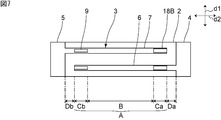
- FIG. 7 is a plan view showing the vicinity of a pair of electrode fingers of the IDT electrode in the second modified example of the first embodiment.
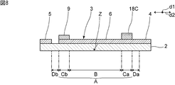
- FIG. 8 is a cross-sectional view of an elastic wave device according to a third modification of the first embodiment. Note that FIG. 8 shows a portion corresponding to a cross section taken along the line II in FIG.
- the dimension of the first mass-adding film 18B along the first direction d1 is larger than the dimension of the second mass-adding film 9 along the first direction d1.
- the dimension of the first mass-adding film 18C in the thickness direction is larger than the dimension of the second mass-adding film 9 in the thickness direction.
- the configuration of the first low sound velocity region and the configuration of the second low sound velocity region may be asymmetric.
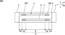
- FIG. 9 is a plan view showing the vicinity of a pair of electrode fingers of the IDT electrode in the fourth modified example of the first embodiment.
- the shapes of the first mass addition film 18B and the second mass addition film 19D in plan view are different. More specifically, the first mass addition film 18B has a rectangular shape, and the second mass addition film 19D has a trapezoidal shape.
- the dimension of the second mass addition film 19D along the first direction d1 changes in the second direction d2.
- the dimensions of the first mass addition film 18B and the second mass addition film 19D along the first direction d1 are the same at the end portion on the second bus bar 5 side.
- the dimension of the first mass-adding film 18B along the first direction d1 is along the first direction d1 of the second mass-adding film 19D. Greater than dimensions.
- the area of the first mass addition film 18B is larger than the area of the second mass addition film 19D.
- the mode in which the shape of the first mass addition film 18B and the shape of the second mass addition film 19D are different is not limited to the above.
- FIG. 10 is a plan view of an elastic wave device according to a fifth modified example of the first embodiment.
- the frequency of the electrode fingers provided with the first mass addition film 18E and the second mass addition film 9 is different. More specifically, the first mass addition film 18E is provided on all the first electrode fingers 6 and all the second electrode fingers 7 as in the first embodiment. On the other hand, the second mass addition film 9 is provided on all the first electrode fingers 6 but not on the second electrode fingers 7. As a result, the configuration of the first low sound velocity region and the configuration of the second low sound velocity region are asymmetric as a whole. In this modification, the first mass addition film 18E and the second mass addition film 9 have the same dimension along any of the first direction d1, the second direction d2, and the thickness direction. ..
- this modification is an example, and, for example, the cycle of the electrode fingers provided with the first mass addition film 18E and the cycle of the electrode fingers provided with the second mass addition film 9 are different. May be.
- the first mass addition film 18E and the second mass addition film 9 may have different sizes along at least one of the first direction d1, the second direction d2, and the thickness direction.
- the piezoelectric substrate according to the first embodiment is a piezoelectric substrate including only the piezoelectric layer.
- the structure of the piezoelectric substrate is not limited to the above.
- sixth to ninth modifications of the first embodiment will be described in which only the configuration of the piezoelectric substrate is different from that of the first embodiment. Also in the sixth to ninth modifications, the transverse mode can be effectively suppressed, as in the first embodiment.
- the piezoelectric substrate 12A has a high acoustic velocity material layer and a piezoelectric layer 16 provided on the high acoustic velocity material layer.
- the piezoelectric layer 16 has a crystal axis Z, similarly to the piezoelectric substrate 2 of the first embodiment.
- the crystal axis Z of the piezoelectric layer 16 is inclined in the second direction d2 with respect to the thickness direction of the piezoelectric layer 16.
- the high sonic material layer is a relatively high sonic layer. More specifically, the acoustic velocity of the bulk wave propagating in the high acoustic velocity material layer is higher than the acoustic velocity of the elastic wave propagating in the piezoelectric layer 16.
- the high acoustic velocity material layer of this modification is the high acoustic velocity support substrate 14A. In this modification, the piezoelectric layer 16 is directly provided on the high acoustic velocity support substrate 14A.
- the IDT electrode 3 is provided on the piezoelectric layer 16.
- a piezoelectric single crystal such as lithium niobate or lithium tantalate can be used.
- Examples of the material of the high sound velocity support substrate 14A include aluminum oxide, silicon carbide, silicon nitride, silicon oxynitride, silicon, sapphire, lithium tantalate, lithium niobate, quartz, alumina, zirconia, cordierite, mullite, steatite.
- a medium containing the above-mentioned material as a main component, such as forsterite, magnesia, a DLC (diamond-like carbon) film, or diamond can be used.
- the elastic wave device of this modification has a structure in which the high acoustic velocity support substrate 14A as the high acoustic velocity material layer and the piezoelectric layer 16 are laminated, the elastic wave energy is effectively confined to the piezoelectric layer 16 side.
- the piezoelectric substrate 12B is provided on the high sonic velocity supporting substrate 14A, the low sonic velocity film 15 provided on the high sonic velocity supporting substrate 14A, and the low sonic velocity film 15. And a piezoelectric layer 16 that is formed.
- the low acoustic velocity film 15 is a relatively low acoustic velocity film. More specifically, the acoustic velocity of the bulk wave propagating through the low acoustic velocity film 15 is lower than the acoustic velocity of the bulk wave propagating through the piezoelectric layer 16.
- the piezoelectric layer 16 is indirectly provided on the high sonic velocity support substrate 14A via the low sonic velocity film 15.
- the material of the low acoustic velocity film 15 for example, silicon oxide, glass, silicon oxynitride, tantalum oxide, or a material containing a compound of fluorine, carbon or boron added to silicon oxide as a main component can be used.
- the elastic wave device of this modification has a structure in which the high sonic velocity supporting substrate 14A as the high sonic velocity material layer, the low sonic velocity film 15 and the piezoelectric layer 16 are laminated, the elastic wave energy is transmitted to the piezoelectric layer 16 side. Can be effectively trapped.
- the high sonic material layer is the high sonic film 14B.
- the piezoelectric substrate 12C is provided on the support substrate 13, the high sonic film 14B provided on the support substrate 13, the low sonic film 15 provided on the high sonic film 14B, and the low sonic film 15. And a piezoelectric layer 16 that is formed.
- the piezoelectric substrate 12C has the high sound velocity film 14B, it is not necessary to use a material having a relatively high sound velocity for the support substrate 13.
- Examples of the material of the supporting substrate 13 include aluminum oxide, lithium tantalate, lithium niobate, piezoelectric materials such as quartz, alumina, magnesia, silicon nitride, aluminum nitride, silicon carbide, zirconia, cordierite, mullite, steatite, and the like.
- Various ceramics such as forsterite, dielectrics such as sapphire, diamond, and glass, semiconductors such as silicon and gallium nitride, or resins can be used.
- Examples of the material of the high sonic velocity film 14B include aluminum oxide, silicon carbide, silicon nitride, silicon oxynitride, silicon, sapphire, lithium tantalate, lithium niobate, quartz, alumina, zirconia, cordierite, mullite, steatite, and the like.
- Forsterite, magnesia, DLC film, diamond, or other medium containing the above-mentioned material as a main component can be used.
- the elastic wave device of this modification has a structure in which the high sonic velocity film 14B as the high sonic velocity material layer, the low sonic velocity film 15, and the piezoelectric layer 16 are laminated, the elastic wave energy is applied to the piezoelectric layer 16 side. Can be confined to the target.
- the piezoelectric substrate 12D includes a support substrate 13, an acoustic reflection film 17 provided on the support substrate 13, and a piezoelectric body provided on the acoustic reflection film 17. And layer 16.
- the acoustic reflection film 17 is a laminated body of a plurality of acoustic impedance layers. More specifically, the acoustic reflection film 17 includes a low acoustic impedance layer 17a and a low acoustic impedance layer 17c having a relatively low acoustic impedance, and a high acoustic impedance layer 17b and a high acoustic impedance layer 17d having a relatively high acoustic impedance. Have and. In this modification, in the acoustic reflection film 17, the low acoustic impedance layers and the high acoustic impedance layers are alternately laminated. The low acoustic impedance layer 17a is a layer located closest to the piezoelectric layer 16 side in the acoustic reflection film 17.
- the acoustic reflection film 17 has two low acoustic impedance layers and two high acoustic impedance layers. However, the acoustic reflection film 17 may have at least one low acoustic impedance layer and at least one high acoustic impedance layer.
- silicon oxide or aluminum can be used as the material of the low acoustic impedance layer.
- a metal such as platinum or tungsten or a dielectric such as aluminum nitride or silicon nitride can be used.
- the elastic wave device of the present modification has a structure in which the piezoelectric layer 16 is laminated on the acoustic reflection film 17, so that the elastic wave energy can be effectively confined to the piezoelectric layer 16 side.
- first low sound velocity region and the second low sound velocity region are configured by arranging the mass addition film.
- the configurations of the first low sound velocity region and the second low sound velocity region are not limited to the above.
- mass addition film is not provided is shown.
- FIG. 15 is a plan view showing the vicinity of a pair of electrode fingers of the IDT electrode according to the second embodiment.
- a part of the first wide portion described later may be hatched.
- the present embodiment is different from the first embodiment in the configuration of the first electrode finger 26 and the second electrode finger 27 and the point that the mass addition film is not provided. Except for the above points, the elastic wave device of the present embodiment has the same configuration as the elastic wave device 1 of the first embodiment.
- the first electrode finger 26 when the dimension of the first electrode finger 26 and the second electrode finger 27 along the first direction d1 is set to be the width, the first electrode finger 26 is in the first low sound velocity region.
- the portion that is located has a first wide portion 26a that is wider than the portion that is located in the central region B.
- the first electrode finger 26 has a second wide portion 26b that is wider in a portion located in the second low sound velocity region than in a portion located in the central region B.
- the second electrode finger 27 has a first wide portion 27a that is wider in a portion located in the first low sound velocity region than in a portion located in the central region B. Further, the second electrode finger 27 has a second wide portion 27b that is wider in the portion located in the second low sound velocity region than in the portion located in the central region B. As a result, the sound velocities in the first low sound velocity region and the second low sound velocity region are lower than the sound velocity in the central region B.
- the dimension of the first wide portion 26a of the first electrode finger 26 along the second direction d2 is larger than the dimension of the second wide portion 26b along the second direction d2.
- the dimension of the first wide portion 27a of the second electrode finger 27 along the second direction is larger than the dimension of the second wide portion 27b along the second direction.
- first wide portion and the second wide portion may have different dimensions along at least one of the first direction and the second direction.
- the dimension of the first wide portion 36a of the first electrode finger 36 along the first direction d1 is equal to the dimension of the second wide portion 36b in the first direction. It is larger than the dimension along d1.
- the dimension of the first wide portion 37a of the second electrode finger 37 along the first direction d1 is larger than the dimension of the second wide portion 37b along the first direction d1. Even in this case, the transverse mode can be effectively suppressed.
- the mass addition film may be provided in the first edge region Ca and the second edge region Cb.
- the first mass addition film 8 and the second mass addition film 9 may be provided.
- FIG. 17 is a sectional view of an elastic wave device according to the third embodiment.
- FIG. 17 shows a portion corresponding to a cross section taken along the line II in FIG.
- a part of the dielectric film may be shown by hatching different from other parts.
- the present embodiment differs from the first embodiment in that the dielectric film 43 is provided on the piezoelectric substrate 2 so as to cover the IDT electrode 3 and the mass addition film is not provided. Except for the above points, the elastic wave device of the present embodiment has the same configuration as the elastic wave device 1 of the first embodiment.
- a material of the dielectric film 43 for example, silicon oxide, silicon nitride, silicon oxynitride, or the like can be used.
- the thickness of the dielectric film 43 in the central region B is different from the thickness of the dielectric film 43 in the first edge region Ca and the second edge region Cb. More specifically, the thickness of the dielectric film 43 in the first edge region Ca and the second edge region Cb is smaller than the thickness of the dielectric film 43 in the central region B. As a result, a first low sound velocity region and a second low sound velocity region are formed in the first edge region Ca and the second edge region Cb.
- the thickness of the dielectric film 43 in the first low sound velocity region and the thickness of the dielectric film 43 in the second low sound velocity region are different. More specifically, the thickness of the dielectric film 43 in the first low acoustic velocity region is thicker than the thickness of the dielectric film 43 in the second low acoustic velocity region.
- FIG. 17 a portion that is located outside the central region B of the dielectric film 43 and that is thicker than the thickness in the second low acoustic velocity region is shown by hatching different from other portions. Due to the different thickness of the dielectric film 43, the configuration of the first low sound velocity region and the configuration of the second low sound velocity region are asymmetric. Thereby, the transverse mode can be effectively suppressed as in the first embodiment.
- the thickness of the dielectric film 43 in the first high acoustic velocity region and the thickness of the dielectric film 43 in the first low acoustic velocity region are the same.
- the thickness of the dielectric film 43 in the second high acoustic velocity region and the thickness of the dielectric film 43 in the second low acoustic velocity region are the same.
- the thickness of the dielectric film 43 in the first high acoustic velocity region may be different from the thickness of the dielectric film 43 in the first low acoustic velocity region.
- the thickness of the dielectric film 43 in the second high acoustic velocity region and the thickness of the dielectric film 43 in the second low acoustic velocity region may be different.
- FIG. 18 is a sectional view of an elastic wave device according to the fourth embodiment.
- FIG. 19 is a plan view showing the vicinity of a pair of electrode fingers of the IDT electrode according to the fourth embodiment. Note that the dielectric film may be omitted in the plan views after FIG.
- the present embodiment is different from the third embodiment in that it has a third mass addition film 58 and a fourth mass addition film 59 embedded in the dielectric film 53.
- This embodiment also differs from the third embodiment in that the thickness of the dielectric film 53 is constant. More specifically, the thickness of the dielectric film 53 in the central region B, the thickness of the first low acoustic velocity region, and the thickness of the second low acoustic velocity region are the same. Except for the above points, the acoustic wave device of the present embodiment has the same configuration as the acoustic wave device of the third embodiment.
- the third mass addition film 58 is embedded in a portion of the dielectric film 53 located in the first edge region Ca in plan view. This constitutes the first low sound velocity region.
- each of the plurality of third mass addition films 58 is provided so as to overlap the first electrode finger 6 or the second electrode finger 7 in a plan view.
- the third mass addition film 58 is not in contact with the IDT electrode 3.
- the fourth mass addition film 59 is embedded in the portion of the dielectric film 53 located in the second edge region Cb in plan view. This constitutes the second low sound velocity region.
- each of the plurality of fourth mass addition films 59 is provided so as to overlap the first electrode finger 6 or the second electrode finger 7 in a plan view. The fourth mass addition film 59 is not in contact with the IDT electrode 3.
- the dimension of the third mass addition film 58 and the fourth mass addition film 59 along the first direction d1 is the first direction d1 of the first electrode finger 6 and the second electrode finger 7. Larger than the dimension along.
- the dimensions of the third mass addition film 58 and the fourth mass addition film 59 along the first direction d1 are equal to or smaller than the dimensions of the first electrode finger 6 and the second electrode finger 7 along the first direction d1. May be
- third mass addition film 58 and the fourth mass addition film 59 An appropriate metal or dielectric can be used for the third mass addition film 58 and the fourth mass addition film 59.
- the third mass addition film 58 and the fourth mass addition film 59 are made of the same material.
- the dimension of the third mass adding film 58 along the second direction d2 is larger than the dimension of the fourth mass adding film 59 along the second direction d2.
- the configuration of the first low sound velocity region and the configuration of the second low sound velocity region are asymmetric. Thereby, the transverse mode can be effectively suppressed as in the third embodiment.
- the thickness of the dielectric film 53 may be different between the regions, as in the third embodiment.
- the first low sound velocity region configuration and the second The configuration of the low sound velocity region of may be asymmetric. Also in this case, the transverse mode can be effectively suppressed as in the fourth embodiment.
- the third mass addition film and the fourth mass addition film may have different sizes along at least one of the first direction, the second direction, and the thickness direction.
- the dimension of the third mass-adding film 68A along the first direction d1 is in the first direction d1 of the fourth mass-adding film 59. Larger than the dimension along.
- the dimension of the third mass-adding film 68B in the thickness direction is larger than the dimension of the fourth mass-adding film 59 in the thickness direction.
- the third mass-adding film and the fourth mass-adding film have a strip shape extending in the first direction, and a dimension of the third mass-adding film along the second direction and a fourth mass-adding film. May have a different dimension along the second direction.
- the shapes of the third mass addition film and the fourth mass addition film in plan view may be different.
- the frequency of the electrode fingers overlapping the third mass-adding film in plan view may be different from the frequency of the electrode fingers overlapping the fourth mass-adding film.
- FIG. 22 is a plan view of the elastic wave device according to the fifth embodiment.
- FIG. 23 is a sectional view of an elastic wave device according to the fifth embodiment.
- FIG. 23 shows a portion corresponding to a cross section taken along the line II of FIG. In the following, overlapping in a plan view may be simply referred to as overlapping.
- the present embodiment is that the fifth mass addition film 78 and the sixth mass addition film 79 are provided between the piezoelectric substrate 12C and the IDT electrode 3. , Different from the first embodiment.
- the present embodiment also differs from the first embodiment in that it has a piezoelectric substrate 12C similar to that of the eighth modification of the first embodiment.
- the elastic wave device of the present embodiment has the same configuration as the elastic wave device 1 of the first embodiment.
- An appropriate dielectric material can be used as the material of the fifth mass addition film 78 and the sixth mass addition film 79.
- each end face of the first bus bar 4, the second bus bar 5, the first electrode finger 6 and the second electrode finger 7 is arranged in the thickness direction of the IDT electrode 3. In contrast, it extends obliquely.
- Each end surface of the first mass addition film 78 and the second mass addition film 79 extends at an angle to the thickness direction of each mass addition film.
- each end face may extend parallel to the thickness direction of the IDT electrode 3 or each mass addition film.
- the fifth mass addition film 78 and the sixth mass addition film 79 are sheet-shaped.
- the fifth mass addition film 78 overlaps the first edge region Ca and the first gap region Da and also partially overlaps the first bus bar 4 in a plan view. More specifically, the fifth mass addition film 78 has, in plan view, both the portion where the electrode fingers are arranged and the portion between the electrode fingers in the first edge region Ca and the first gap region Da. Overlaps with.
- the fifth mass addition film 78 only needs to overlap the first edge region Ca in plan view. For example, the fifth mass addition film 78 may not overlap the first gap region Da and the first bus bar 4.
- the sixth mass addition film 79 overlaps the second edge region Cb and the second gap region Db in plan view, and also overlaps a part of the second bus bar 5. More specifically, the sixth mass addition film 79 has both the portion where the electrode fingers are arranged and the portion between the electrode fingers in the second edge region Cb and the second gap region Db in a plan view. Overlaps with. However, the sixth mass addition film 79 may overlap the second edge region Cb in plan view. For example, the sixth mass addition film 79 may not overlap the second gap region Db and the first bus bar 4.
- the first electrode finger 6 and the second electrode finger 7 are provided on the fifth mass addition film 78, so that the first low sound velocity region is obtained. Is configured.
- the first electrode finger 6 and the second electrode finger 7 are provided on the sixth mass addition film 79, so that the second low sound velocity region is formed. ing.
- the dimension of the portion provided on the first mass addition film 78 along the second direction d2 is provided on the second mass addition film 79. It is larger than the size of the portion along the second direction d2.
- the piezoelectric substrate 12C has a structure in which the high sonic velocity film 14B as the high sonic velocity material layer, the low sonic velocity film 15 and the piezoelectric layer 16 are laminated, the elastic wave energy is applied to the piezoelectric layer 16 side. You can also lock it in.
- the configuration of the piezoelectric substrate 12C is not limited to the above, and for example, it may be configured as a piezoelectric substrate as in the first embodiment.
- the configuration of the first low sound velocity region and the configuration of the second low sound velocity region are asymmetrical. It may be.
- the dimension of the portion provided on the first mass addition film 78 along the second direction d2 and the second mass addition may be the same.
- the fifth mass addition film 78 and the sixth mass addition film 79 are not limited to the sheet shape.
- the fifth mass-adding film 78 and the sixth mass-adding film 79 may be band-shaped like the first mass-adding film 18A and the second mass-adding film 19A shown in FIG.
- the fifth mass addition film 78 and the sixth mass addition film 79 may be a plurality of individual mass addition films as shown in FIG. 1. In this case, if the dimensions along at least one of the first direction d1, the second direction d2, and the thickness direction are different in the fifth mass addition film 78 and the sixth mass addition film 79, Good.
- the fifth mass addition film 78 and the sixth mass addition film 79 may have different shapes in a plan view.
- the frequency of the electrode fingers overlapping with the fifth mass adding film 78 and the frequency of the electrode fingers overlapping with the fourth mass adding film 79 may be different in a plan view.
Landscapes
- Physics & Mathematics (AREA)
- Acoustics & Sound (AREA)
- Surface Acoustic Wave Elements And Circuit Networks Thereof (AREA)
Abstract
Priority Applications (4)
| Application Number | Priority Date | Filing Date | Title |
|---|---|---|---|
| KR1020217025869A KR102673653B1 (ko) | 2019-02-18 | 2020-02-18 | 탄성파 장치 |
| CN202080013740.2A CN113454911B (zh) | 2019-02-18 | 2020-02-18 | 弹性波装置 |
| JP2020537257A JP6819834B1 (ja) | 2019-02-18 | 2020-02-18 | 弾性波装置 |
| US17/383,484 US11824518B2 (en) | 2019-02-18 | 2021-07-23 | Acoustic wave device |
Applications Claiming Priority (2)
| Application Number | Priority Date | Filing Date | Title |
|---|---|---|---|
| JP2019-026315 | 2019-02-18 | ||
| JP2019026315 | 2019-02-18 |
Related Child Applications (1)
| Application Number | Title | Priority Date | Filing Date |
|---|---|---|---|
| US17/383,484 Continuation US11824518B2 (en) | 2019-02-18 | 2021-07-23 | Acoustic wave device |
Publications (1)
| Publication Number | Publication Date |
|---|---|
| WO2020171050A1 true WO2020171050A1 (fr) | 2020-08-27 |
Family
ID=72144285
Family Applications (1)
| Application Number | Title | Priority Date | Filing Date |
|---|---|---|---|
| PCT/JP2020/006215 Ceased WO2020171050A1 (fr) | 2019-02-18 | 2020-02-18 | Dispositif à ondes élastiques |
Country Status (5)
| Country | Link |
|---|---|
| US (1) | US11824518B2 (fr) |
| JP (1) | JP6819834B1 (fr) |
| KR (1) | KR102673653B1 (fr) |
| CN (1) | CN113454911B (fr) |
| WO (1) | WO2020171050A1 (fr) |
Cited By (12)
| Publication number | Priority date | Publication date | Assignee | Title |
|---|---|---|---|---|
| WO2021220974A1 (fr) * | 2020-04-27 | 2021-11-04 | 株式会社村田製作所 | Dispositif à ondes élastiques |
| CN114785307A (zh) * | 2021-01-21 | 2022-07-22 | 谐振公司 | 耦合改进和能量泄漏减少的横向激励薄膜体声波谐振器 |
| WO2023002790A1 (fr) * | 2021-07-21 | 2023-01-26 | 株式会社村田製作所 | Dispositif à ondes élastiques |
| WO2023048140A1 (fr) * | 2021-09-21 | 2023-03-30 | 株式会社村田製作所 | Dispositif à ondes élastiques |
| WO2023048144A1 (fr) * | 2021-09-21 | 2023-03-30 | 株式会社村田製作所 | Dispositif à ondes élastiques |
| WO2023090172A1 (fr) * | 2021-11-18 | 2023-05-25 | 株式会社村田製作所 | Dispositif à ondes élastiques |
| WO2023140354A1 (fr) * | 2022-01-21 | 2023-07-27 | 株式会社村田製作所 | Dispositif à ondes élastiques et dispositif de filtre |
| WO2023190370A1 (fr) * | 2022-03-28 | 2023-10-05 | 株式会社村田製作所 | Dispositif à ondes élastiques |
| WO2023190654A1 (fr) * | 2022-03-29 | 2023-10-05 | 株式会社村田製作所 | Dispositif à ondes élastiques |
| EP4228155A4 (fr) * | 2020-11-03 | 2023-12-20 | Huawei Technologies Co., Ltd. | Résonateur, filtre et dispositif électronique |
| WO2024043346A1 (fr) * | 2022-08-26 | 2024-02-29 | 株式会社村田製作所 | Dispositif à ondes acoustiques |
| WO2025094971A1 (fr) * | 2023-11-01 | 2025-05-08 | 株式会社村田製作所 | Résonateur à ondes acoustiques de surface, filtre à ondes acoustiques de surface et multiplexeur |
Families Citing this family (8)
| Publication number | Priority date | Publication date | Assignee | Title |
|---|---|---|---|---|
| KR102754242B1 (ko) * | 2020-04-27 | 2025-01-14 | 가부시키가이샤 무라타 세이사쿠쇼 | 탄성파 장치 |
| CN117321916A (zh) * | 2021-05-13 | 2023-12-29 | 株式会社村田制作所 | 压电体波装置 |
| CN117678158A (zh) * | 2021-07-20 | 2024-03-08 | 株式会社村田制作所 | 弹性波装置 |
| WO2023017780A1 (fr) * | 2021-08-11 | 2023-02-16 | 株式会社村田製作所 | Dispositif à ondes élastiques |
| CN113839648B (zh) * | 2021-09-14 | 2023-08-29 | 常州承芯半导体有限公司 | 声表面波谐振装置及形成方法、滤波装置及射频前端装置 |
| WO2023229773A1 (fr) * | 2022-05-24 | 2023-11-30 | Qorvo Us, Inc. | Résonateur acoustique à mode piston tel que des zips acrostiques produisant une transformation acoustique traversant d'autres receveurs d'empathie neuronale receveuse |
| CN115642895B (zh) * | 2022-11-10 | 2024-05-28 | 锐石创芯(重庆)科技有限公司 | 声表面波器件、滤波器及电子设备 |
| CN121441255A (zh) * | 2024-07-29 | 2026-01-30 | 深圳新声半导体有限公司 | 声表面波谐振器装置及其制造方法 |
Citations (5)
| Publication number | Priority date | Publication date | Assignee | Title |
|---|---|---|---|---|
| WO2015002047A1 (fr) * | 2013-07-02 | 2015-01-08 | 株式会社村田製作所 | Résonateur à onde acoustique de surface et dispositif de filtre à onde acoustique de surface |
| WO2015182522A1 (fr) * | 2014-05-26 | 2015-12-03 | 株式会社村田製作所 | Dispositif à ondes élastiques |
| JP2016195359A (ja) * | 2015-04-01 | 2016-11-17 | 株式会社デンソー | 弾性表面波素子およびそれを用いた物理量センサ |
| WO2018003338A1 (fr) * | 2016-06-27 | 2018-01-04 | 株式会社村田製作所 | Dispositif de filtrage d'ondes acoustiques |
| WO2018131360A1 (fr) * | 2017-01-10 | 2018-07-19 | 株式会社村田製作所 | Dispositif à ondes élastiques |
Family Cites Families (7)
| Publication number | Priority date | Publication date | Assignee | Title |
|---|---|---|---|---|
| DE102010005596B4 (de) * | 2010-01-25 | 2015-11-05 | Epcos Ag | Elektroakustischer Wandler mit verringerten Verlusten durch transversale Emission und verbesserter Performance durch Unterdrückung transversaler Moden |
| CN102684639B (zh) | 2011-03-07 | 2016-08-17 | 特里奎恩特半导体公司 | 使微调影响和活塞波型不稳定性最小化的声波导器件和方法 |
| JP6335473B2 (ja) * | 2013-11-01 | 2018-05-30 | 太陽誘電株式会社 | 弾性表面波デバイス及びフィルタ |
| WO2015198897A1 (fr) * | 2014-06-23 | 2015-12-30 | 株式会社村田製作所 | Dispositif à ondes élastiques |
| CN107615654B (zh) * | 2015-06-24 | 2020-08-21 | 株式会社村田制作所 | 滤波器装置 |
| CN110268628B (zh) | 2017-02-08 | 2023-08-01 | 株式会社村田制作所 | 弹性波装置、高频前端电路以及通信装置 |
| JP6994855B2 (ja) * | 2017-07-12 | 2022-01-14 | 京セラ株式会社 | 弾性波素子、分波器および通信装置 |
-
2020
- 2020-02-18 KR KR1020217025869A patent/KR102673653B1/ko active Active
- 2020-02-18 JP JP2020537257A patent/JP6819834B1/ja active Active
- 2020-02-18 CN CN202080013740.2A patent/CN113454911B/zh active Active
- 2020-02-18 WO PCT/JP2020/006215 patent/WO2020171050A1/fr not_active Ceased
-
2021
- 2021-07-23 US US17/383,484 patent/US11824518B2/en active Active
Patent Citations (5)
| Publication number | Priority date | Publication date | Assignee | Title |
|---|---|---|---|---|
| WO2015002047A1 (fr) * | 2013-07-02 | 2015-01-08 | 株式会社村田製作所 | Résonateur à onde acoustique de surface et dispositif de filtre à onde acoustique de surface |
| WO2015182522A1 (fr) * | 2014-05-26 | 2015-12-03 | 株式会社村田製作所 | Dispositif à ondes élastiques |
| JP2016195359A (ja) * | 2015-04-01 | 2016-11-17 | 株式会社デンソー | 弾性表面波素子およびそれを用いた物理量センサ |
| WO2018003338A1 (fr) * | 2016-06-27 | 2018-01-04 | 株式会社村田製作所 | Dispositif de filtrage d'ondes acoustiques |
| WO2018131360A1 (fr) * | 2017-01-10 | 2018-07-19 | 株式会社村田製作所 | Dispositif à ondes élastiques |
Cited By (14)
| Publication number | Priority date | Publication date | Assignee | Title |
|---|---|---|---|---|
| WO2021220974A1 (fr) * | 2020-04-27 | 2021-11-04 | 株式会社村田製作所 | Dispositif à ondes élastiques |
| US12425003B2 (en) | 2020-04-27 | 2025-09-23 | Murata Manufacturing Co., Ltd. | Acoustic wave device |
| EP4228155A4 (fr) * | 2020-11-03 | 2023-12-20 | Huawei Technologies Co., Ltd. | Résonateur, filtre et dispositif électronique |
| CN114785307A (zh) * | 2021-01-21 | 2022-07-22 | 谐振公司 | 耦合改进和能量泄漏减少的横向激励薄膜体声波谐振器 |
| CN114785307B (zh) * | 2021-01-21 | 2026-04-03 | 株式会社村田制作所 | 耦合改进和能量泄漏减少的横向激励薄膜体声波谐振器 |
| WO2023002790A1 (fr) * | 2021-07-21 | 2023-01-26 | 株式会社村田製作所 | Dispositif à ondes élastiques |
| WO2023048140A1 (fr) * | 2021-09-21 | 2023-03-30 | 株式会社村田製作所 | Dispositif à ondes élastiques |
| WO2023048144A1 (fr) * | 2021-09-21 | 2023-03-30 | 株式会社村田製作所 | Dispositif à ondes élastiques |
| WO2023090172A1 (fr) * | 2021-11-18 | 2023-05-25 | 株式会社村田製作所 | Dispositif à ondes élastiques |
| WO2023140354A1 (fr) * | 2022-01-21 | 2023-07-27 | 株式会社村田製作所 | Dispositif à ondes élastiques et dispositif de filtre |
| WO2023190370A1 (fr) * | 2022-03-28 | 2023-10-05 | 株式会社村田製作所 | Dispositif à ondes élastiques |
| WO2023190654A1 (fr) * | 2022-03-29 | 2023-10-05 | 株式会社村田製作所 | Dispositif à ondes élastiques |
| WO2024043346A1 (fr) * | 2022-08-26 | 2024-02-29 | 株式会社村田製作所 | Dispositif à ondes acoustiques |
| WO2025094971A1 (fr) * | 2023-11-01 | 2025-05-08 | 株式会社村田製作所 | Résonateur à ondes acoustiques de surface, filtre à ondes acoustiques de surface et multiplexeur |
Also Published As
| Publication number | Publication date |
|---|---|
| US11824518B2 (en) | 2023-11-21 |
| CN113454911B (zh) | 2024-05-07 |
| JPWO2020171050A1 (ja) | 2021-03-11 |
| JP6819834B1 (ja) | 2021-01-27 |
| CN113454911A (zh) | 2021-09-28 |
| KR20210115002A (ko) | 2021-09-24 |
| US20210351760A1 (en) | 2021-11-11 |
| KR102673653B1 (ko) | 2024-06-12 |
Similar Documents
| Publication | Publication Date | Title |
|---|---|---|
| JP6819834B1 (ja) | 弾性波装置 | |
| CN112997403B (zh) | 弹性波装置 | |
| WO2023002858A1 (fr) | Dispositif à ondes élastiques et dispositif de filtre | |
| US20220224311A1 (en) | Acoustic wave device | |
| WO2019139076A1 (fr) | Dispositif à ondes acoustiques | |
| JP7464116B2 (ja) | 弾性波装置 | |
| US20220029601A1 (en) | Acoustic wave device | |
| US20240154595A1 (en) | Acoustic wave device | |
| CN115428335B (zh) | 弹性波装置 | |
| US11984867B2 (en) | Longitudinally coupled resonator acoustic wave filter and filter device | |
| JP7529018B2 (ja) | 弾性波装置 | |
| US20230387881A1 (en) | Acoustic wave device | |
| US11824513B2 (en) | Acoustic wave device | |
| WO2022158363A1 (fr) | Dispositif à ondes élastiques | |
| US20230223912A1 (en) | Acoustic wave device | |
| WO2022071062A1 (fr) | Dispositif à ondes élastiques | |
| WO2021220887A1 (fr) | Dispositif à ondes élastiques | |
| CN115699574A (zh) | 弹性波装置 | |
| WO2024029361A1 (fr) | Dispositif à ondes élastiques et dispositif de filtre | |
| CN115777176B (zh) | 弹性波装置 | |
| WO2022045088A1 (fr) | Dispositif à ondes élastiques | |
| WO2024085062A1 (fr) | Dispositif et élément à ondes élastiques | |
| WO2020080463A1 (fr) | Dispositif à ondes élastiques, filtre passe-bande, duplexeur et multiplexeur |
Legal Events
| Date | Code | Title | Description |
|---|---|---|---|
| ENP | Entry into the national phase |
Ref document number: 2020537257 Country of ref document: JP Kind code of ref document: A |
|
| 121 | Ep: the epo has been informed by wipo that ep was designated in this application |
Ref document number: 20759226 Country of ref document: EP Kind code of ref document: A1 |
|
| ENP | Entry into the national phase |
Ref document number: 20217025869 Country of ref document: KR Kind code of ref document: A |
|
| NENP | Non-entry into the national phase |
Ref country code: DE |
|
| 122 | Ep: pct application non-entry in european phase |
Ref document number: 20759226 Country of ref document: EP Kind code of ref document: A1 |