WO2020171130A1 - 制御回路、表示装置、電子機器、投射型表示装置および制御方法 - Google Patents
制御回路、表示装置、電子機器、投射型表示装置および制御方法 Download PDFInfo
- Publication number
- WO2020171130A1 WO2020171130A1 PCT/JP2020/006590 JP2020006590W WO2020171130A1 WO 2020171130 A1 WO2020171130 A1 WO 2020171130A1 JP 2020006590 W JP2020006590 W JP 2020006590W WO 2020171130 A1 WO2020171130 A1 WO 2020171130A1
- Authority
- WO
- WIPO (PCT)
- Prior art keywords
- liquid crystal
- line
- pixels
- crystal panel
- pixel
- Prior art date
- Legal status (The legal status is an assumption and is not a legal conclusion. Google has not performed a legal analysis and makes no representation as to the accuracy of the status listed.)
- Ceased
Links
Images


Classifications
-
- G—PHYSICS
- G09—EDUCATION; CRYPTOGRAPHY; DISPLAY; ADVERTISING; SEALS
- G09G—ARRANGEMENTS OR CIRCUITS FOR CONTROL OF INDICATING DEVICES USING STATIC MEANS TO PRESENT VARIABLE INFORMATION
- G09G3/00—Control arrangements or circuits, of interest only in connection with visual indicators other than cathode-ray tubes
- G09G3/20—Control arrangements or circuits, of interest only in connection with visual indicators other than cathode-ray tubes for presentation of an assembly of a number of characters, e.g. a page, by composing the assembly by combination of individual elements arranged in a matrix no fixed position being assigned to or needed to be assigned to the individual characters or partial characters
- G09G3/34—Control arrangements or circuits, of interest only in connection with visual indicators other than cathode-ray tubes for presentation of an assembly of a number of characters, e.g. a page, by composing the assembly by combination of individual elements arranged in a matrix no fixed position being assigned to or needed to be assigned to the individual characters or partial characters by control of light from an independent source
- G09G3/36—Control arrangements or circuits, of interest only in connection with visual indicators other than cathode-ray tubes for presentation of an assembly of a number of characters, e.g. a page, by composing the assembly by combination of individual elements arranged in a matrix no fixed position being assigned to or needed to be assigned to the individual characters or partial characters by control of light from an independent source using liquid crystals
- G09G3/3611—Control of matrices with row and column drivers
- G09G3/3648—Control of matrices with row and column drivers using an active matrix
-
- G—PHYSICS
- G02—OPTICS
- G02F—OPTICAL DEVICES OR ARRANGEMENTS FOR THE CONTROL OF LIGHT BY MODIFICATION OF THE OPTICAL PROPERTIES OF THE MEDIA OF THE ELEMENTS INVOLVED THEREIN; NON-LINEAR OPTICS; FREQUENCY-CHANGING OF LIGHT; OPTICAL LOGIC ELEMENTS; OPTICAL ANALOGUE/DIGITAL CONVERTERS
- G02F1/00—Devices or arrangements for the control of the intensity, colour, phase, polarisation or direction of light arriving from an independent light source, e.g. switching, gating or modulating; Non-linear optics
- G02F1/01—Devices or arrangements for the control of the intensity, colour, phase, polarisation or direction of light arriving from an independent light source, e.g. switching, gating or modulating; Non-linear optics for the control of the intensity, phase, polarisation or colour
- G02F1/13—Devices or arrangements for the control of the intensity, colour, phase, polarisation or direction of light arriving from an independent light source, e.g. switching, gating or modulating; Non-linear optics for the control of the intensity, phase, polarisation or colour based on liquid crystals, e.g. single liquid crystal display cells
- G02F1/133—Constructional arrangements; Operation of liquid crystal cells; Circuit arrangements
- G02F1/136—Liquid crystal cells structurally associated with a semi-conducting layer or substrate, e.g. cells forming part of an integrated circuit
- G02F1/1362—Active matrix addressed cells
- G02F1/1368—Active matrix addressed cells in which the switching element is a three-electrode device
-
- G—PHYSICS
- G09—EDUCATION; CRYPTOGRAPHY; DISPLAY; ADVERTISING; SEALS
- G09G—ARRANGEMENTS OR CIRCUITS FOR CONTROL OF INDICATING DEVICES USING STATIC MEANS TO PRESENT VARIABLE INFORMATION
- G09G3/00—Control arrangements or circuits, of interest only in connection with visual indicators other than cathode-ray tubes
- G09G3/20—Control arrangements or circuits, of interest only in connection with visual indicators other than cathode-ray tubes for presentation of an assembly of a number of characters, e.g. a page, by composing the assembly by combination of individual elements arranged in a matrix no fixed position being assigned to or needed to be assigned to the individual characters or partial characters
- G09G3/34—Control arrangements or circuits, of interest only in connection with visual indicators other than cathode-ray tubes for presentation of an assembly of a number of characters, e.g. a page, by composing the assembly by combination of individual elements arranged in a matrix no fixed position being assigned to or needed to be assigned to the individual characters or partial characters by control of light from an independent source
- G09G3/36—Control arrangements or circuits, of interest only in connection with visual indicators other than cathode-ray tubes for presentation of an assembly of a number of characters, e.g. a page, by composing the assembly by combination of individual elements arranged in a matrix no fixed position being assigned to or needed to be assigned to the individual characters or partial characters by control of light from an independent source using liquid crystals
Definitions
- the present disclosure relates to a control circuit, a display device, an electronic device, a projection display device, and a control method.
- Patent Document 1 describes a liquid crystal display device capable of improving a moving image quality by inserting a black display screen between images.
- the LCD panel has the problem that moving image afterimages and trailing may occur when displaying moving images.
- a technique for suppressing such a moving image afterimage and trailing is desired.
- An object of the present disclosure is to provide a control circuit, a display device, an electronic device, a projection display device, and a control method capable of suppressing a moving image afterimage and trailing.
- the control circuit controls the driving of the liquid crystal panel so that lines of the same gradation having a width of 1 pixel or more and 10 pixels or less are transferred in the screen.
- the second disclosure is LCD panel, A drive unit that drives the liquid crystal panel, And a control circuit for controlling the drive of the liquid crystal panel via the drive unit,
- the control circuit is a display device that controls driving of the liquid crystal panel so that lines of the same gradation having a width of 1 pixel or more and 10 pixels or less are transferred.
- the third disclosure is Equipped with a display device,
- the display device is LCD panel, A drive unit that drives the liquid crystal panel, And a control circuit for controlling the drive of the liquid crystal panel via the drive unit,
- the control circuit is an electronic device that controls driving of the liquid crystal panel so that lines of the same gradation having a width of 1 pixel or more and 10 pixels or less are transferred.
- the fourth disclosure is Illumination optics, A plurality of liquid crystal panels that generate image light by modulating the light from the illumination optical system, A control circuit for controlling the driving of a plurality of liquid crystal panels, A projection optical system for projecting image light generated by a plurality of liquid crystal panels, The control circuit is a projection display device that controls driving of the liquid crystal panel so that lines of the same gradation having a width of 1 pixel or more and 10 pixels or less are transferred.
- the fifth disclosure is This is a control method for controlling the driving of the liquid crystal panel so that lines of the same gradation having a width of 1 pixel or more and 10 pixels or less are transferred.
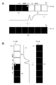
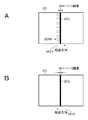
- FIG. 1A is a schematic diagram showing a state where liquid crystal molecules are tilted in an alignment direction by pretilt between adjacent pixels due to an influence of a horizontal electric field.
- FIG. 1B is a schematic diagram showing a state in which liquid crystal molecules between adjacent pixels are influenced by a lateral electric field and are tilted in a direction opposite to the alignment direction by pretilt.
- FIG. 2 is a schematic diagram showing an example in which a black pattern moves leftward in a screen displayed in white.
- FIG. 3A is a plan view showing an example of a region 50R in FIG. 2 in a stopped state (initial state) of a black pattern.
- FIG. 3B is a plan view showing an example of the region 50R in FIG.
- FIG. 3C is a plan view showing an example of the region 50R in FIG. 2 after two fields (33.3 msec) from the start of movement of the black pattern.
- FIG. 3D is a plan view showing an example of the region 50R in FIG. 2 after three fields (50 msec) from the start of movement of the black pattern.
- FIG. 4A is a diagram schematically illustrating a cross section taken along line IVA-IVA of FIG. 3A.
- FIG. 4B is a diagram schematically illustrating a cross section along IVB-IVB in FIG. 3B.
- FIG. 4C is a diagram schematically illustrating a cross section taken along line IVC-IVC of FIG. 3C.
- FIG. 4D is a diagram schematically illustrating a cross section taken along line IVD-IVD of FIG. 3A.
- FIG. 5A is a schematic diagram showing the relationship between the alignment direction of liquid crystal molecules and the directions in which afterimages and tailing occur.
- FIG. 5B is a schematic diagram showing an example in which the black pattern is moved to the left in the liquid crystal panel in the alignment direction shown in FIG. 5A.
- FIG. 5C is a schematic view showing an example in which the liquid crystal panel in the alignment direction shown in FIG. 5A has a black pattern moved upward.
- FIG. 5D is a schematic view showing an example of moving the black pattern to the right in the liquid crystal panel in the alignment direction shown in FIG. 5A.
- FIG. 5A is a schematic diagram showing the relationship between the alignment direction of liquid crystal molecules and the directions in which afterimages and tailing occur.
- FIG. 5B is a schematic diagram showing an example in which the black pattern is moved to the left in the liquid crystal panel in the alignment direction shown in FIG. 5
- FIG. 5E is a schematic diagram showing an example in which the black pattern is moved downward in the liquid crystal panel in the alignment direction shown in FIG. 5A.
- FIG. 6A is a schematic diagram showing the relationship between the alignment direction of liquid crystal molecules and the directions in which afterimages and tailing occur.
- FIG. 6B is a schematic view showing an example in which the black pattern is moved to the left in the liquid crystal panel in the alignment direction shown in FIG. 6A.
- FIG. 6C is a schematic view showing an example in which the black pattern is moved upward in the liquid crystal panel in the alignment direction shown in FIG. 6A.
- FIG. 6D is a schematic view showing an example in which the black pattern is moved to the right in the liquid crystal panel in the alignment direction shown in FIG. 6A.
- FIG. 6A is a schematic diagram showing the relationship between the alignment direction of liquid crystal molecules and the directions in which afterimages and tailing occur.
- FIG. 6B is a schematic view showing an example in which the black pattern is moved to the left in the liquid crystal panel in
- FIG. 6E is a schematic view showing an example in which the black pattern is moved downward in the liquid crystal panel in the alignment direction shown in FIG. 6A.
- FIG. 7A is a schematic diagram showing the relationship between the alignment direction of liquid crystal molecules and the directions in which afterimages and tailing occur.
- FIG. 7B is a schematic view showing an example in which the black pattern is moved to the left in the liquid crystal panel in the alignment direction shown in FIG. 7A.
- FIG. 7C is a schematic view showing an example in which the black pattern is moved upward in the liquid crystal panel in the alignment direction shown in FIG. 7A.
- FIG. 7D is a schematic view showing an example in which the black pattern is moved to the right in the liquid crystal panel in the alignment direction shown in FIG. 7A.
- FIG. 7A is a schematic diagram showing the relationship between the alignment direction of liquid crystal molecules and the directions in which afterimages and tailing occur.
- FIG. 7B is a schematic view showing an example in which the black pattern is moved to the left in the liquid crystal panel in
- FIG. 7E is a schematic diagram showing an example in which the black pattern is moved downward in the liquid crystal panel in the alignment direction shown in FIG. 7A.
- FIG. 8A is a schematic diagram showing the relationship between the alignment direction of liquid crystal molecules and the directions in which afterimages and tailing occur.
- FIG. 8B is a schematic view showing an example in which the black pattern is moved to the left in the liquid crystal panel in the alignment direction shown in FIG. 8A.
- FIG. 8C is a schematic view showing an example in which the liquid crystal panel in the alignment direction shown in FIG. 8A has a black pattern moved upward.
- FIG. 8D is a schematic view showing an example in which the black pattern is moved to the right in the liquid crystal panel in the alignment direction shown in FIG. 8A.
- FIG. 8A is a schematic diagram showing the relationship between the alignment direction of liquid crystal molecules and the directions in which afterimages and tailing occur.
- FIG. 8B is a schematic view showing an example in which the black pattern is moved to the left in the liquid crystal panel in
- FIG. 8E is a schematic view showing an example in which the black pattern is moved downward in the liquid crystal panel in the alignment direction shown in FIG. 8A.
- FIG. 9A is a plan view showing an example of the region 50R in FIG. 2 in the state one field (16.6 msec) after the start of the movement of the black pattern.
- 9B is a diagram schematically showing a cross section taken along line IXB-IXB of FIG. 9A.
- FIG. 10A is a schematic diagram showing an example in which a horizontal line of a liquid crystal panel is temporarily displayed in black.
- FIG. 10B is a schematic diagram showing an example in which the vertical line of the liquid crystal panel is temporarily displayed in black.
- FIG. 11 is a schematic diagram showing an example in which the entire screen is temporarily displayed in black.
- FIG. 12 is a block diagram showing an example of the configuration of the liquid crystal display device according to the first embodiment of the present disclosure.
- FIG. 13 is a diagram showing an example of an equivalent circuit of the liquid crystal panel.
- FIG. 14 is a schematic diagram showing an example of the configuration of a liquid crystal panel.
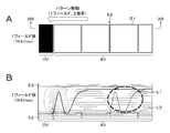
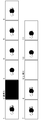
- FIG. 15A is a schematic diagram showing an example of transferring a black line in the vertical direction.
- FIG. 15B is a schematic diagram showing an example of transferring a black line in the horizontal direction.
- FIG. 16 is a schematic diagram for explaining the relationship between the transfer direction of a black line and the occurrence of a moving image afterimage and trailing due to the transfer of a black line.
- FIG. 17A is a schematic diagram showing a transfer direction of a black line in which a moving image afterimage and tailing occur.
- FIG. 17B is a schematic diagram showing a transfer direction of a black line in which the occurrence of a moving image afterimage and trailing is suppressed.
- FIG. 18A is a schematic diagram showing a transfer direction of a black line in which a moving image afterimage and trailing are generated.
- FIG. 18B is a schematic diagram showing a transfer direction of a black line in which the occurrence of a moving image afterimage and trailing is suppressed.
- FIG. 19A is a schematic diagram showing a first example of a method of inserting a black line.
- FIG. 19A is a schematic diagram showing a first example of a method of inserting a black line.
- FIG. 19B is a schematic diagram showing a second example of a method of inserting a black line.
- FIG. 19C is a schematic diagram showing a third example of a method of inserting a black line.
- FIG. 20 is a timing chart for explaining the first example of the operation of the liquid crystal display device according to the first embodiment of the present disclosure.
- FIG. 21 is a timing chart for explaining the second example of the operation of the liquid crystal display device according to the first embodiment of the present disclosure.
- FIG. 22 is a timing chart for explaining the third example of the operation of the liquid crystal display device according to the first embodiment of the present disclosure.
- FIG. 23 is a diagram showing an example of an equivalent circuit of a liquid crystal panel according to a modification.
- FIG. 24 is a timing chart for explaining an example of the operation of the liquid crystal display device according to the modification.
- FIG. 25 is a schematic diagram showing an example of inserting an image of full black display.
- FIG. 26 is a schematic diagram showing an example of inserting an image of full white display.
- FIG. 27 is a schematic diagram showing an example of inserting an image of full black display and an image of full white display.
- FIG. 28 is a schematic diagram showing an example of inserting the same halftone image over the entire surface.
- 29A and 29B are schematic diagrams showing an example of inserting an image of full black display.
- FIG. 30 is a block diagram showing an example of the configuration of a display device according to the second embodiment of the present disclosure.
- FIG. 31 is a diagram showing an example of an equivalent circuit of a liquid crystal panel.
- FIG. 32 is a schematic diagram showing an example of transferring a black line in the vertical direction.
- FIG. 33 is a timing chart for explaining the first example of the operation of the liquid crystal display device according to the second embodiment of the present disclosure.
- FIG. 34 is a timing chart for explaining the second example of the operation of the liquid crystal display device according to the second embodiment of the present disclosure.
- FIG. 35 is a timing chart for explaining the third example of the operation of the liquid crystal display device according to the second embodiment of the present disclosure.
- FIG. 36 is a diagram showing an example of an equivalent circuit of a liquid crystal panel according to a modification.
- FIG. 37 is a timing chart showing an example of the operation of the liquid crystal panel according to the modification.
- FIG. 38 is a diagram showing an example of an equivalent circuit of a liquid crystal panel according to a modification.
- FIG. 39 is a diagram showing an example of an equivalent circuit of a liquid crystal panel according to a modification.
- FIG. 40 is a block diagram showing an example of the configuration of a liquid crystal display device according to the third embodiment of the present disclosure.
- FIG. 41 is a diagram showing an example of an equivalent circuit of a liquid crystal panel.
- FIG. 42 is a timing chart for explaining the first example of the operation of the liquid crystal display device according to the third embodiment of the present disclosure.
- FIG. 43 is a timing chart for explaining the second example of the operation of the liquid crystal display device according to the third embodiment of the present disclosure.
- FIG. 44 is a timing chart for explaining the third example of the operation of the liquid crystal display device according to the third embodiment of the present disclosure.
- FIG. 45 is a diagram showing an example of an equivalent circuit of a liquid crystal panel according to a modification.
- FIG. 46 is a timing chart showing an example of the operation of the liquid crystal panel according to the modification.
- FIG. 47 is a block diagram showing an example of the configuration of a liquid crystal display device according to the fourth embodiment of the present disclosure.
- FIG. 48 is a diagram showing an example of an equivalent circuit of a liquid crystal panel.
- FIG. 49 is a timing chart for explaining the first example of the operation of the liquid crystal display device according to the fourth embodiment of the present disclosure.
- FIG. 45 is a diagram showing an example of an equivalent circuit of a liquid crystal panel according to a modification.
- FIG. 46 is a timing chart showing an example of the operation of the liquid crystal panel according to the modification.
- FIG. 47 is a block diagram showing an example of the configuration of a liquid crystal display device according
- FIG. 50 is a timing chart for explaining another example of the operation of the liquid crystal display device according to the fourth embodiment of the present disclosure.
- FIG. 51 is a timing chart for explaining the second example of the operation of the liquid crystal display device according to the fourth embodiment of the present disclosure.
- 52A, 52B, 52C, and 52D are schematic diagrams each showing an example of inserting a black display in an area where a moving object exists.
- FIG. 53 is a perspective view showing an example of a configuration of an electronic device according to the fifth embodiment of the present disclosure.
- FIG. 54 is a perspective view showing an example of the configuration of the electronic device according to the sixth embodiment of the present disclosure.
- FIG. 55 is a schematic diagram showing an example of the configuration of a projector according to the seventh embodiment of the present disclosure.
- the potential difference between the counter substrate 53 and the TFT (Thin Film Transistor) substrate 52 in black display is, for example, 0 V
- the potential difference between the counter substrate 53 and the TFT substrate 52 in white display is, for example, 4 V. Is.
- the black pattern 71 moves to the left in the white-displayed screen 50 ⁇ /b>A.
- the cause of occurrence of () is described.
- “left direction”, “right direction”, “upward direction”, and “downward direction” respectively mean directions toward left, right, up, and down in the drawings. ..
- the color of the pattern 71 is black and the background of the pattern 71 is white unless otherwise specified.
- the part 62 where the disclination 61 occurs (the boundary between the black display and the white display) 62 also moves to the left. At this time, the time until the disclination 61 returns to the normal orientation depends on the moving speed of the black pattern 71.
- the disclination 61 in a moving image in which the generation portion 62 of the disclination 61 moves at a moving speed of one field and one pixel, the disclination 61 returns to a normal orientation state. Takes the longest to get to. Therefore, in a moving image in which the generation portion 62 of the disclination 61 moves at a moving speed of one field and one pixel, moving image afterimage/tailing occurs. That is, the generation portion 62 of the disclination 61 is recognized as a thick black region in a still image, whereas it is recognized as a tail in a moving image. 4A to 4D, the line L1 indicates the transmittance and the line L2 indicates the equipotential surface.
- the moving image afterimage/tailing described above occurs when a specific alignment direction of the liquid crystal molecules 54 and a specific movement direction of the pattern 71 are combined.
- the pattern 71 moves upward or rightward at a moving speed of one field and one pixel. In that case, a moving image afterimage/tailing 72 occurs.
- FIGS. 5B and 5E when the pattern 71 moves leftward or downward at a moving speed of one field and one pixel, the occurrence of a moving image afterimage/tailing 72 is suppressed.
- the pattern 71 moves leftward or upward at a moving speed of one field and one pixel. In that case, a moving image afterimage/tailing 72 occurs.
- FIGS. 6D and 6E when the pattern 71 moves rightward or downward at a moving speed of one field and one pixel, the occurrence of a moving image afterimage/tailing 72 is suppressed.
- the pattern 71 moves leftward or downward at a moving speed of one field and one pixel. In that case, a moving image afterimage/tailing 72 occurs.
- FIGS. 7C and 7D when the pattern 71 moves upward or rightward at a moving speed of one field and one pixel, the occurrence of a moving image afterimage/tailing 72 is suppressed.
- the pattern 71 moves rightward or downward at a moving speed of one field and one pixel. In that case, a moving image afterimage/tailing 72 occurs.
- FIGS. 8B and 8C when the pattern 71 moves leftward or upward at a moving speed of one field and one pixel, generation of a moving image afterimage/tailing 72 is suppressed.
- the occurrence of moving image afterimage/trailing 72 depends on the moving speed of the pattern 71.
- the moving image afterimage/tailing 72 occurs when the pattern 71 moves at a moving speed of one field and one pixel.
- the moving image afterimage/tailing 72 Outbreaks are greatly mitigated. This is because the portion where the disclination 61 has occurred in the current field is not affected by the disclination 61 from the pattern 71 moved in the next field, that is, locally reset in the raster display of the same gradation. Is.
- the pattern moving speed depends on the displayed moving image, it is desirable to consider an improvement measure for the moving image afterimage/trailing 72 on the premise of one field and one pixel.
- the moving image afterimage/trailing 72 can be reset by displaying a raster of the same gradation and eliminating the lateral electric field.
- a black raster raster of the same gradation
- FIG. 10A once the horizontal line 51LA is set to black display only (that is, only the same gradation), the horizontal electric field between the left and right adjacent pixels 51 can be reset.
- FIG. 10B when the vertical line 51LB is set to only black display (only the same gradation), the horizontal electric field between vertically adjacent pixels 51 can be reset.
- a black raster raster of the same gradation
- the present inventors have examined a liquid crystal display device capable of suppressing moving image afterimage/tailing 72 while suppressing a decrease in screen brightness. As a result, they have come to find a liquid crystal display device that transfers lines of the same gradation into the screen. In the first embodiment, such a liquid crystal display device will be described.
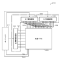
- the display device 10 is applicable as a light valve of a three-plate type projector (projection type display device).
- the display device 10 includes a controller 11, a liquid crystal panel 20, and a drive unit 30.
- the liquid crystal panel 20 may be a transmissive type or a reflective type.
- the display device 10 may include a light source (not shown) behind the liquid crystal panel 20 as needed.
- the controller 11 corresponds to a specific but not limitative example of “control circuit” in one embodiment of the present disclosure.
- the liquid crystal panel 20 has, for example, normally black transmittance characteristics or reflectance characteristics.
- normally black refers to an optical characteristic in which the transmittance or the reflectance is minimum when no voltage is applied, and black display is performed.
- the liquid crystal panel 20 may have, for example, normally white transmittance characteristics or reflectance characteristics.
- normally white refers to an optical characteristic in which the transmittance or reflectance is maximized when no voltage is applied and white display is achieved.
- the liquid crystal panel 20 generates image light by electrically changing the polarization state of light when a voltage is applied.
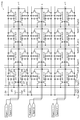
- FIG. 13 is a diagram showing an example of an equivalent circuit of the liquid crystal panel 20.
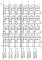
- the liquid crystal panel 20 includes a plurality of main scanning lines (first scanning lines) 21 extending in the row direction, a plurality of sub-scanning lines (second scanning lines) 22 extending in the row direction, and rows.
- the plurality of storage capacitor lines 24 extending in the direction, the plurality of signal lines 23 extending in the column direction, and the main scanning line 21 and the signal line 23 are provided one at each intersection. It has a plurality of pixels 25.
- the same number of main scanning lines 21 and sub-scanning lines 22 are provided.
- Each pixel 25 is input from the liquid crystal cell 26, the main transistor (first transistor) 27 that writes the voltage of the signal line 23 to the liquid crystal cell 26 based on the signal input from the main scanning line 21, and the sub scanning line 22.
- the liquid crystal cell 26 has a voltage transistor (second transistor) 28 for writing the voltage of the storage capacitor line 24 to the liquid crystal cell 26 based on the signal, and a capacitor element 29 connected in parallel to the liquid crystal cell 26.
- Mgate(n), Sgate(n), and Sig(m) are the output of the main vertical drive circuit 31 (that is, the voltage of the main scanning line 21) and the output of the sub vertical drive circuit 32 (that is, the sub scanning line). 22) and the output of the horizontal drive circuit 33 (that is, the voltage of the horizontal drive circuit 33).
- pix(n,m) represents the pixel 25 at the intersection of the nth main scanning line 21 from the top and the mth signal line 23 from the left. It should be noted that in the following description, these reference numerals respectively represent the same as the above.
- FIG. 14 is a schematic diagram showing an example of the configuration of the liquid crystal panel 20.
- the liquid crystal panel 20 includes, for example, a liquid crystal layer 26A including liquid crystal molecules 26D, a plurality of pixel electrodes 26B sandwiching the liquid crystal layer 26A, and a counter electrode 26C.
- the liquid crystal panel 20 may further include a polarizing plate, for example.
- the driving method of the liquid crystal panel 20 is, for example, VA (Vertical Alignment) mode, TN (Twisted Nematic) mode, IPS (In Plane Switching) mode, FFS (Fringe Field Switching) mode, STN (Super Twisted Nematic) mode, or It is an ECB (Electrically Controlled Birefringence) mode.
- VA Very Alignment
- TN Transmission Nematic
- IPS In Plane Switching
- FFS Frringe Field Switching
- STN Super Twisted Nematic
- ECB Electrodefringence
- the main transistor 27 and the sub-transistor 28 are composed of, for example, thin film transistors (TFTs).
- TFTs thin film transistors
- the gate electrode of the main transistor 27 is connected to the main scanning line 21, the source electrode (or drain electrode) is connected to the signal line 23, and the drain electrode (or source electrode) is connected to the pixel electrode 26B of the liquid crystal cell 26. ..
- the gate electrode of the sub-transistor 28 is connected to the sub-scanning line 22, the source electrode (or drain electrode) is connected to the pixel electrode 26B of the liquid crystal cell 26, and the drain electrode (or source electrode) is connected to the storage capacitance line 24.
- the storage capacitor line 24 may be connected to a counter voltage generation circuit (hereinafter referred to as “VCOM circuit”) (not shown) included in the controller 11.
- VCOM circuit counter voltage generation circuit
- the first electrode of the capacitance element 29 is connected to the pixel electrode 26B of the liquid crystal cell 26, and the second electrode is connected to the storage capacitance line 24.
- the storage capacitor line 24 is connected to a storage capacitor voltage generation circuit (hereinafter referred to as “VCS circuit”) (not shown) included in the controller 11.
- VCS circuit generates a predetermined holding capacitance voltage Vcs and applies the voltage to the pixel electrode 26B of the liquid crystal cell 26 and the second electrode of the capacitance element 29.
- the VCS circuit may be provided outside the controller 11.
- the counter electrode 26C of the liquid crystal cell 26 is connected to the VCOM circuit included in the controller 11.
- the VCOM circuit generates a predetermined common voltage Vcom and applies it to the counter electrode 26C of the liquid crystal cell 26.
- the VCOM circuit may be provided outside the controller 11.
- the voltage applied to the pixel electrode 26B (the potential difference between the counter electrode 26C and the pixel electrode 26B) is changed according to the gradation of the video signal. This makes it possible to control the alignment direction of the liquid crystal molecules 26D and control the amount of light emitted from the pixels 25 including the liquid crystal molecules 26D (that is, display gradation). An image can be displayed by controlling the alignment direction of the liquid crystal molecules 26D in each of the plurality of pixels 25 of the liquid crystal panel 20.
- the orientation direction of the liquid crystal molecules 26D is defined by the polar angle ⁇ and the azimuth angle ⁇ of the spherical coordinate system shown in FIG.
- the polar angle ⁇ can be changed according to the potential difference (absolute value) between the counter electrode (common electrode) 26C and the pixel electrode 26B.
- the potential difference absolute value
- the polar angle ⁇ increases and the display gradation increases.
- the azimuth angle ⁇ becomes a specific angle (pretilt azimuth angle) due to the weak alignment regulating force of the alignment films formed on the surfaces of the counter electrode 26C and the pixel electrode 26B.
- the horizontal direction on the display surface of the liquid crystal panel 20 is the x-axis direction
- the horizontal direction of the liquid crystal panel 20 is the y-axis
- the direction perpendicular to the display surface of the liquid crystal panel 20 is the z-axis direction.
- the polar angle ⁇ is an angle based on the z axis
- the azimuth angle ⁇ is an angle based on the x axis direction.
- the directions in which the azimuth angle ⁇ is 0° and 180° are referred to as the first horizontal direction HD1 and the second horizontal direction HD2, respectively, and the azimuth angle ⁇ is 90°.
- the direction of 270° may be referred to as a first vertical direction VD1 and a second vertical direction VD2.
- the drive unit 30 drives the liquid crystal panel 20 under the control of the controller 11. More specifically, the drive unit 30 causes the liquid crystal panel 20 to generate image light based on a video signal input from the outside by driving each pixel 25 by active matrix driving.
- the driving unit 30 includes a main vertical driving circuit (first vertical driving circuit) 31 connected to the plurality of main scanning lines 21 and a sub-scanning line driving circuit (second vertical driving circuit) connected to the plurality of sub-scanning lines. Circuit 32) and a horizontal drive circuit 33 connected to a plurality of signal lines.
- the main vertical drive circuit 31 operates based on a control signal supplied from the controller 11, and applies a drive pulse Mgate(n) for scanning the pixels 25 line-sequentially to the liquid crystal panel 20 via each main scan line 21. Output in parallel.
- the sub-vertical drive circuit 32 operates based on a control signal supplied from the controller 11, and applies a drive pulse Sgate(n) for scanning the pixels 25 line-sequentially to the liquid crystal cell 26 via each sub-scan line 22. Output in parallel.
- the horizontal drive circuit 33 operates based on the control signal supplied from the controller 11, and outputs the signal voltage Sig(m) for each line in parallel to the liquid crystal cell 26 via each signal line 23.
- the signal voltage Sig(m) has a peak value or pulse width according to the gradation of the video signal input from the outside.
- the controller 11 controls the liquid crystal panel 20 via the drive unit 30.
- the controller 11 is composed of, for example, an IC (Integrated Circuit) or the like.
- the controller 11 controls the drive unit 30 to perform active matrix drive control of each pixel 25 by the field inversion drive method.
- the field inversion drive refers to drive in which a signal voltage Sig(m) whose polarity is inverted with respect to the common voltage Vcom of the liquid crystal cell 26 is applied to the liquid crystal cell 26 every one field (1F) period.
- the controller 11 controls the driving of the liquid crystal panel 20 so that a black line (hereinafter simply referred to as “black line”) 20L is transferred in one direction within the display screen.
- black line hereinafter simply referred to as “black line”
- the controller 11 may transfer the black line 20L extending in the horizontal direction in the vertical direction (first vertical direction VD1 or second vertical direction VD2) within the display screen.
- the black line 20L extending in the vertical direction may be transferred in the horizontal direction (first horizontal direction HD1 or second horizontal direction HD2) within the display screen.
- the black line 20L corresponds to a specific but not limitative example of “line having the same gradation” in one embodiment of the present disclosure.
- the width W of the black line 20L is 1 pixel or more and 10 pixels or less, preferably 2 pixels or more and 10 pixels or less.
- the width W of the black line 20L is 1 pixel or more, the occurrence of moving image afterimage/tailing can be suppressed.
- the black line 20L of 1 pixel is transferred in the vertical direction of the display screen, when the object moves horizontally in the screen at a moving speed of 1 pixel per field, the The influence between the disclination portions can be suppressed. Therefore, it is possible to suppress the occurrence of moving image afterimage/tailing in the horizontal direction.
- the black line 20L of one pixel is transferred in the horizontal direction of the display screen, the disclination before and after one field when the object moves vertically in the screen at the moving speed of one pixel in one field The influence between the parts can be suppressed. Therefore, it is possible to suppress the occurrence of moving image afterimage/tailing in the vertical direction.
- width W of the black line 20L is 10 pixels or less, it is possible to effectively suppress the decrease in contrast.
- the black line 20L is repeatedly transferred on the display screen at a specified cycle.
- the one-time moving distance of the black line 20L is one pixel, and the moving of the line is performed at regular intervals. That is, the transfer rate of the black line 20L is one pixel in the vertical direction or the horizontal direction in a specified period, and the transfer of the black line 20L is continuously performed in the vertical direction or the horizontal direction.
- the specified period is, for example, one field or n horizontal periods (n is an integer of 1 or more).
- a moving image afterimage/tailing due to the transfer of the black line 20L may occur depending on the transfer direction of the black line 20L.
- the transfer direction of the black line 20L is the first vertical direction VD1 as shown in FIG. 17A, a moving image afterimage/tailing 20M occurs.
- the transfer direction of the black line 20L is the second vertical direction VD2 as shown in FIG. 17B
- the occurrence of the moving image afterimage/tailing 20M is suppressed.
- the transfer direction of the black line 20L is the first vertical direction VD1 as shown in FIG. 18A
- a moving image afterimage/tailing 20M occurs.
- the transfer direction of the black line 20L is the second horizontal direction HD2 as shown in FIG. 18B
- the occurrence of the moving image afterimage/tailing 20M is suppressed.
- the transfer of the black line 20L is performed according to the azimuth angle ⁇ of the liquid crystal molecule as in the following relationships (1) to (4). It is preferable to set the direction.
- the transfer direction of the black line 20L is preferably the second vertical direction VD2 or the second horizontal direction HD2 (FIG. 17B, 18B, 5B, 5E).
- the transfer direction of the black line 20L is preferably the second vertical direction VD2 or the first horizontal direction HD1 (FIG. 6D, see FIG. 6E).
- the transfer direction of the black line 20L is preferably the first vertical direction VD1 or the first horizontal direction HD1 (FIG. 7C, see FIG. 7D).
- the transfer direction of the black line 20L is preferably the first vertical direction VD1 or the second horizontal direction HD2 (FIG. 8B, see FIG. 8C).
- the transfer frequency of the black line 20L is set in consideration of suppression of burn-in of the liquid crystal panel 20 and suppression of reduction in brightness.
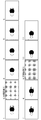
- a black line 20L may be inserted in each field (1F).
- the black line 20L may be inserted in the first field of each block.
- the black lines 20L are alternately inserted in the positive field and the negative field.
- FIG. 19C when one block is composed of three or more consecutive fields (1F), the black line 20L is inserted at the beginning of each block and the next field. May be.
- the “positive field” refers to a field in which a signal voltage Sig(m) having a positive polarity with respect to the common voltage Vcom of the liquid crystal cell 26 is applied to the liquid crystal cell 26, and “negative field”.
- the “field” means a field in which a signal voltage Sig(m) having a negative polarity with respect to the common voltage Vcom of the liquid crystal cell 26 is applied to the liquid crystal cell 26.
- 19A to 19 the symbols "+” and "-" attached to each field indicate the polarities of the signal voltage Sig(m) applied to the liquid crystal cell 26 in each field.
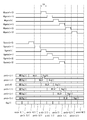
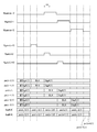
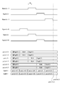
- the sub-vertical drive circuit 32 sets the voltage Sgate(n) of the n-th sub-scan line 22 from the top to the High level for one horizontal period (1H).
- the sub-transistors 28 of the pixels (n,1), (n,2), (n,3),... Are turned on, and the pixels (n,1), (n,2), (n,2).
- the storage capacitor voltage Vcs of the storage capacitor line 24 is applied to 3),....
- the pixels (n, 1), (n, 2), (n, 3),... are displayed in black.
- the main vertical drive circuit 31 sets the voltage Mgate(n) of the nth main scanning line 21 from the top for one horizontal period at the timing when the voltage Sgate(n) of the nth subscanning line 22 from the top becomes Low level. Set to High level.
- the main transistors 27 of the pixels (n,1), (n,2), (n,3),... Are turned on for one horizontal period, and the pixels (n,1), (n,2) are turned on. , (N, 3),..., Voltages Sig(1), Sig(2), Sig(3),... Of the signal lines 23 are respectively applied to the pixels (n, 1), (n, 2). ), (n, 3),... Provide a predetermined gradation display.
- predetermined gradation display means gradation display excluding black display for suppressing the occurrence of moving image afterimage/tailing. That is, it means gradation display based on a video signal supplied to the display device 10 from the outside.
- the sub-vertical driving circuit 32 sets the voltage Sgate(n) of the n-th sub-scanning line 22 from the top to the Low level, and sets the voltage Sgate(n+1) of the n+1-th sub-scanning line 22 from the top in one horizontal period, Set to High level. Further, the main vertical drive circuit 31 sets the voltage Mgate(n+1) of the n+1th main scanning line 21 from the top to the High level for one horizontal period at the timing when the voltage Sgate(n+1) of the sub scanning line 22 becomes the Low level. To do.
- the main vertical drive circuit 31 drives the uppermost to lowermost main scanning lines 21 as described above, and the sub-vertical drive circuit 32 drives the uppermost to lowermost subscanning lines 22 as described above.
- the black line 20L having a width of 1 pixel is continuously transferred in the vertical direction (that is, at a speed of 1 pixel in one horizontal period).
- the driving operation of the sub-vertical driving circuit 32 is the same as the above-mentioned “example of transferring a line having a width of one pixel in the vertical direction”, and therefore the description thereof will be omitted.
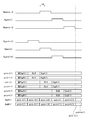
- the main vertical drive circuit 31 detects the voltage Mgate(n) of the n-th main scanning line 21 from the top after one horizontal period has elapsed since the voltage Sgate(n) of the n-th sub-scanning line 22 from the top becomes Low level. Is set to High level for one horizontal period. As a result, the main transistors 27 of the pixels (n,1), (n,2), (n,3),... Are turned on for one horizontal period, and the pixels (n,1), (n,2) are turned on. , (N, 3),..., Voltages Sig(1), Sig(2), Sig(3),... Of the respective signal lines 23 are applied to the pixels (n, 1), (n, 3). 2), (n, 3),... Are predetermined gradation display. Therefore, the period in which the pixels (n, 1), (n, 2), (n, 3),... Are black-displayed is two horizontal periods (2H).
- the main vertical drive circuit 31 sets the voltage Mgate(n+1) of the n+1th main scanning line 21 from the top for one horizontal period after one horizontal period has passed since the voltage Sgate(n+1) of the sub-scanning line 22 was set to the Low level. Set to High level.
- the main vertical drive circuit 31 drives the uppermost to lowermost main scanning lines 21 as described above, and the sub-vertical drive circuit 32 drives the uppermost to lowermost subscanning lines 22 as described above.
- the black line 20L having a width of 2 pixels is continuously transferred in the vertical direction (that is, at a speed of 1 pixel in one horizontal period).
- the sub-vertical drive circuit 32 sets the voltage Sgate(n) of the n-th sub-scan line 22 from the top to the High level for two horizontal periods.
- the main transistors 27 of the pixels (n, 1), (n, 2), (n, 3),... Are turned on, and the pixels (n, 1), (n, 2), (n, 2).
- the storage capacitor voltage Vcs of the storage capacitor line 24 is applied to 3),....
- the pixels (n, 1), (n, 2), (n, 3),... are displayed in black.
- the main vertical drive circuit 31 sets the voltage Mgate(n) of the nth main scanning line 21 from the top for one horizontal period at the timing when the voltage Sgate(n) of the nth subscanning line 22 from the top becomes Low level. Set to High level.
- the main transistors 27 of the pixels (n,1), (n,2), (n,3),... Are turned on for one horizontal period, and the pixels (n,1), (n,2) are turned on. , (N, 3),..., Voltages Sig(1), Sig(2), Sig(3),. 2), (n, 3),... Are predetermined gradation display. Therefore, the period in which the pixels (n, 1), (n, 2), (n, 3),... Are black-displayed is two horizontal periods.
- the sub-vertical drive circuit 32 sets the voltage Sgate(n+1) of the (n+1)th sub-scanning line 22 from the top after one horizontal period has elapsed since the voltage Sgate(n) of the n-th sub-scanning line 22 from the top is set to the High level. It is set to High level for two horizontal periods. Further, the main vertical drive circuit 31 sets the voltage Mgate(n+1) of the n+1th main scanning line 21 from the top to the horizontal level at the timing when the voltage Sgate(n+1) of the n+1th subscanning line 22 from the top becomes the Low level. High level for a period.
- the main vertical drive circuit 31 drives the uppermost to lowermost main scanning lines 21 as described above, and the sub-vertical drive circuit 32 drives the uppermost to lowermost subscanning lines 22 as described above.
- the black line 20L having a width of 2 pixels is continuously transferred in the vertical direction (that is, at a speed of 1 pixel in one horizontal period).
- the display device 10 includes a liquid crystal panel 20, a drive unit 30 that drives the liquid crystal panel 20, and a controller (control circuit) 11 that controls the drive of the liquid crystal panel 20 via the drive unit 30.
- Prepare The controller 11 controls the driving of the liquid crystal panel 20 so that the black line 20L having a width W of 1 pixel or more and 10 pixels or less is periodically transferred in the vertical direction or the horizontal direction.
- the black line 20L is transferred and the moving image afterimage/tailing is suppressed, compared to the display device in which the image of full black display is inserted and the moving image afterimage/tailing is suppressed. As a result, it is possible to suppress a decrease in brightness.
- the width W of the black line 20L is a width of 1 pixel or more and 10 pixels or less, it is possible to suppress a decrease in luminance due to the transfer of the black line 20L. For example, when a black line 20L having a width W of 2 pixels is transferred, the decrease in brightness is about 0.1%, and there is almost no effect on the display quality of the liquid crystal panel 20. It is also possible to adjust the display time of the black line 20L according to the liquid crystal response speed.
- Modification 2 In the first embodiment, a case where the display device 10 includes a main vertical drive circuit 31 that outputs a drive pulse to the main scanning line 21 and a sub vertical drive circuit 32 that outputs a drive pulse to the sub scanning line 22 will be described.
- the configuration of the display device 10 is not limited to this.
- the display device 10 may include one vertical drive circuit that outputs a drive pulse to each of the main scanning line 21 and the sub scanning line 22, instead of the main vertical driving circuit 31 and the sub vertical driving circuit 32.
- FIG. 23 shows an example of the configuration of a liquid crystal panel 20A that transfers a black line 20L with a varying width W.
- the sub-scanning lines 22 that are vertically adjacent to each other form a pair in order from the top, and the sub-scanning lines 22 that form this pair are connected at one end.
- the same drive pulse is output from the sub-vertical drive circuit 32 to the sub-scanning lines 22 forming a pair. Therefore, the number of sub-scanning lines 22 connected to the sub-vertical drive circuit 32 in the liquid crystal panel 20A is half the number of sub-scanning lines 22 connected to the sub-vertical drive circuit 32 in the liquid crystal panel 20 of the first embodiment. It has become. Therefore, in the liquid crystal panel 20A, the configuration of the leading wiring can be simplified as compared with the liquid crystal panel 20.
- FIG. 24 is a timing chart for explaining the operation of the liquid crystal panel 20A that transfers the black line 20L in which the width W changes.
- the sub-vertical drive circuit 32 sets the voltage Sgate(n) of the n-th sub-scanning line 22 and the n+1-th sub-scanning line 22 from the top to the High level for one horizontal period.
- the transistor 28 is turned on, and pixels (n,1), (n,2), (n,3),..., Pixels (n+1,1), (n+1,2), (n+1,3),...
- the storage capacitor voltage Vcs of the storage capacitor line 24 is applied to.
- pixels (n,1), (n,2), (n,3),..., Pixels (n+1,1), (n+1,2), (n+1,3),... Are black. Will be displayed.
- the main vertical drive circuit 31 generates the voltage Mgate of the nth main scanning line 21 from the top at the timing when the voltage Sgate(n) of the nth subscanning line 22 and the n+1th subscanning line 22 becomes the Low level.
- (N) is set to High level for one horizontal period.
- the main transistors 27 of the pixels (n,1), (n,2), (n,3),... Are turned on for one horizontal period, and the pixels (n,1), (n,2) are turned on.
- (N, 3) ..., Voltages Sig(1), Sig(2), Sig(3),... Of the respective signal lines 23 are applied to the pixels (n, 1), (n, 3). 2), (n, 3),... Are predetermined gradation display. Therefore, the period in which the pixels (n, 1), (n, 2), (n, 3),... Are black-displayed is one horizontal period.
- the main vertical drive circuit 31 is configured to detect the n+1th main scanning line from the top after one horizontal period has elapsed since the voltage Sgate(n) of the nth subscanning line 22 and the n+1th subscanning line 22 has become Low level.
- the voltage Mgate(n+1) on the line 21 is set to High level for one horizontal period.
- the main transistors 27 of the pixels (n+1,1), (n+1,2), (n+1,3),... Are turned on for one horizontal period, and the pixels (n+1,1), (n+1,2) are turned on. , (N+1, 3),... To which respective voltages Sig(1), Sig(2), Sig(3),...
- the period in which the pixels (n+1, 1), (n+1, 2), (n+1, 3),... Are black-displayed is two horizontal periods.
- the sub-vertical drive circuit 32 sets the voltage Sgate(n) of the n-th sub-scanning line 22 and the n+1-th sub-scanning line 22 to the Low level, and after one horizontal period elapses, the n+2-th and n+3-th sub-scanning lines from the top.
- the voltage Sgate(n+2) of the sub scanning line 22 is set to High level for one horizontal period.
- the main vertical drive circuit 31 outputs the voltage Mgate of the n+2th main scanning line 21 from the top at the timing when the voltage Sgate(n+2) of the n+2th subscanning line 22 and the n+3th subscanning line 22 from the top becomes Low level. (N) is set to High level for one horizontal period. In addition, the main vertical drive circuit 31 is configured to move from the voltage level Sgate(n) of the n+2th sub-scanning line 22 and the n+3th sub-scanning line 22 from the Low level to one horizontal period, and then to the n+3th sub-scanning line from the top. The voltage Mgate(n+3) of the main scanning line 21 is set to High level for one horizontal period.
- the main vertical drive circuit 31 drives the uppermost to lowermost main scanning lines 21 as described above, and the sub-vertical drive circuit 32 drives the uppermost to lowermost subscanning lines 22 as described above.
- the black line 20L whose width W changes is continuously transferred in the vertical direction (that is, at the speed of one pixel in one horizontal period).
- the controller 11 controls the drive of the liquid crystal panel so that the black line 20L is periodically transferred has been described, but the black raster insertion method is not limited to this. ..
- the controller may control the driving of the liquid crystal panel so that an image of full-field black display for one field is periodically displayed.
- the entire black display screen is displayed at a rate of one in three or more fields.
- the controller may control the drive of the liquid crystal panel so that the image of the entire white display for one field is periodically displayed.
- the controller controls the driving of the liquid crystal panel so that an image of full black display for one field and an image of full white display for one field are alternately and periodically displayed. Good.
- the controller controls the driving of the liquid crystal panel so that an image of full black display for one field and an image of full white display for one field are alternately and periodically displayed.
- the controller controls the driving of the liquid crystal panel so that an image of full black display for one field and an image of full white display for one field are alternately and periodically displayed.
- a decrease in luminance as compared with the case where only the screen of full black display is periodically displayed.
- an image of full black display or a screen of full white display is displayed at a rate of one in three or more fields.
- the controller may control the driving of the liquid crystal panel so that the same halftone image for one field is displayed periodically.
- the same halftone screen is displayed in one area in three or more fields.
- the image of full black display for one field when an image of full black display for one field is inserted, the image of full black display for one field alternates between a positive field and a negative field as shown in FIG. 29A. It is preferably inserted periodically. Since the number of positive fields and the number of negative fields are the same by inserting the image of full black display in this way, burn-in of the liquid crystal panel can be suppressed. It should be noted that the same image insertion operation as in the case of the above-described image of full black display may be performed even when the image of full white display or the same halftone screen of the entire screen is displayed.
- an entirely black display screen is displayed in two fields (that is, a set of a positive field and a negative field) from the beginning of each block. It is preferable that the controller controls the driving of the liquid crystal panel so that is inserted. Since the number of positive fields and the number of negative fields are the same by inserting the image of full black display in this way, burn-in of the liquid crystal panel can be suppressed. It should be noted that the same image insertion operation as in the case of the above-described image of full black display may be performed even when the image of full white display or the same halftone screen of the entire screen is displayed.
- the black line 20L is transferred in the first vertical direction VD1 or the first horizontal direction HD1 at a speed of one pixel in one horizontal period, a moving image residual image caused by the line transfer of the black line 20L -Tailing occurs (see FIGS. 17A and 18A). Therefore, when the azimuth angle ⁇ of the liquid crystal molecule 26D is in the range of 0° ⁇ 90°, the transfer direction of the black line 20L is preset to the second vertical direction VD2 or the second horizontal direction HD2. Preferably.
- the transfer direction of the black line 20L is bidirectional (for example, the first vertical direction VD1 and the second vertical direction VD1). There is a vertical direction VD2). Therefore, moving image afterimage/tailing may occur depending on the transfer direction of the black line 20L.
- the present inventors diligently studied a transfer method in the transfer direction of the black line 20L that can suppress the occurrence of the afterimage of moving images and trailing as described above.
- a transfer method in the transfer direction of the black line 20L that can suppress the occurrence of the afterimage of moving images and trailing as described above.
- the black line 20L having a width of 2 pixels or more so that the movement distance for one time is 2 pixels or more (for example, at a speed of 2 pixels or more in one horizontal period, a width of 2 pixels or more
- the occurrence of a moving image afterimage/tailing can be suppressed regardless of the transfer direction of the black line 20L.
- a display device adopting such a transfer method will be described.
- the display device 110 includes a controller 111, a liquid crystal panel 120, and a drive unit 130.
- the same parts as those in the first embodiment are designated by the same reference numerals and the description thereof will be omitted.
- FIG. 31 is a diagram showing an example of an equivalent circuit of the liquid crystal panel 120.
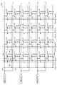
- the liquid crystal panel 120 includes a plurality of main scanning lines (first scanning lines) 121 extending in the row direction, a plurality of sub-scanning lines (second scanning lines) 122 extending in the row direction, and rows.
- the plurality of storage capacitor lines 24 the plurality of signal lines (first signal lines) 123 that extend in the column direction, and the plurality of signal lines (second signal lines) that extend in the column direction.
- Pixel 25, and a plurality of pixels 25 provided one at each position where the even-numbered (n+1-th) main scanning line 121 and the signal line 124 intersect from each other.
- Each of the plurality of signal lines 124 is provided adjacent to the plurality of signal lines 123.
- the vertically adjacent main scanning lines 121 form a pair in order from the top, and the main scanning lines 121 forming this pair are connected at one end.
- the same drive pulse is output from the main vertical drive circuit 131 to the main scanning lines 121 forming a pair. Therefore, the number of main scanning lines 121 connected to the main vertical driving circuit 31 in the liquid crystal panel 120 is half the number of main scanning lines 21 connected to the main vertical driving circuit 131 in the liquid crystal panel 20 of the first embodiment. It has become. Therefore, in the liquid crystal panel 120, the configuration of the leading wiring of the main scanning line 121 can be simplified as compared with the liquid crystal panel 20.
- Sub-scanning lines 122 that are vertically adjacent to each other form a pair in order from the top, and the sub-scanning lines 122 that form this pair are connected at one end.
- the same drive pulse is output from the sub-vertical drive circuit 132 to the sub-scanning lines 122 forming a pair. Therefore, the number of the sub-scanning lines 122 connected to the sub-vertical drive circuit 132 in the liquid crystal panel 120 is half the number of the sub-scanning lines 22 connected to the sub-vertical drive circuit 32 in the liquid crystal panel 20 of the first embodiment. It has become. Therefore, in the liquid crystal panel 20A, the configuration of the lead wiring of the sub-scanning line 122 can be simplified as compared with the liquid crystal panel 20.
- the source electrode (or drain electrode) of the main transistor 27 is connected to the signal line 23.
- the source electrode (or drain electrode) of the main transistor 27 is connected to the signal line 124.
- the driving unit 130 includes a main vertical driving circuit (first vertical driving circuit) 131 connected to the plurality of main scanning lines 121 and a sub-scanning line driving circuit (second vertical driving circuit) connected to the plurality of sub-scanning lines 122.
- Drive circuit) 132 a horizontal drive circuit (first horizontal drive circuit) 133 connected to the plurality of signal lines 123, and a horizontal drive circuit (second horizontal drive circuit) 134 connected to the plurality of signal lines 124. And have.
- the main vertical drive circuit 131 and the sub-vertical drive circuit 132 are different from the main vertical drive circuit 31 and the sub-vertical drive circuit 32 in the first embodiment except that the number of main scanning lines 21 that output a drive pulse is different. It is the same.
- the horizontal drive circuit 133 operates based on a control signal supplied from the controller 111, and applies the signal voltage SigA(m) to the odd-numbered pixels pix(n, 1) and pix(n) from the top via the signal lines 123. 2),... are output in parallel.
- the horizontal drive circuit 133 operates based on the control signal supplied from the controller 11, and applies the signal voltage SigB(m) to each of the even-numbered pixels pix(n+1, 1) and pix(n+1) from the top via each signal line 124. 2),... are output in parallel.
- the signal voltage SigA(m) and the signal voltage SigA(m) have a peak value or a pulse width according to the gradation of a video signal input from the outside.
- the controller 111 controls the driving of the liquid crystal panel 20 so that the black line 20L having a width W of 2 pixels or more and 10 pixels or less is periodically transferred in the vertical direction or the horizontal direction within the display screen.
- the moving distance of the black line 20L once is, as shown in FIG. 32, two pixels or more and the width of the black line 20L or less (specifically, the number of pixels of the black line 20L in the width direction of the black line 20L or less).
- the line is moved every specified period. That is, the transfer rate of the black line 20L is 2 pixels or more in the vertical direction or the horizontal direction in the specified period and is less than or equal to the width of the black line 20L, and the black line 20L is discontinuously transferred in the vertical direction or the horizontal direction.
- the specified period is, for example, one field or n horizontal periods (n is an integer of 1 or more).
- the moving distance of the black line 20L once is not less than 2 pixels and not more than the width of the black line 20L, a gap is not formed between the black lines 20L before and after the moving, and the black line 20L is not formed. 20L is transferred without a gap in the screen. However, if the black line 20L is transferred at a speed of 2 pixels or more in the specified period, the black line 20L before and after the movement may partially overlap.
- the sub-vertical drive circuit 132 sets the voltage Sgate(n) of the n-th sub-scan line 122 and the n+1-th sub-scan line 122 from the top to the High level for one horizontal period.
- the holding capacitance voltage Vcs of the holding capacitance line 24 is applied. Therefore, the pixels (n, 1), (n, 2),... And the pixels (n+1, 1), (n+1, 2),.
- the main vertical drive circuit 131 when the voltage Sgate(n) of the n-th sub-scanning line 122 and the n+1-th sub-scanning line 122 becomes Low level, the n-th main scanning line 121 and the n+1-th sub-scanning line from the top.
- the voltage Mgate(n) of the main scanning line 121 is set to High level for two horizontal periods.
- the main transistors 27 of the pixels (n, 1), (n, 2),... Are turned on for two horizontal periods, and the pixels (n, 1), (n, 2),.
- the voltages SigA(1), SigA(2),... Of the signal line 123 are applied, and the pixels (n, 1), (n, 2),.
- the main transistors 27 of the pixels (n+1,1), (n+1,2),... are turned on for two horizontal periods, and the signals (n+1,1), (n+1,2),.
- the voltages SigB(1), SigB(2),... Of the line 124 are applied, and the pixels (n+1,1), (n+1,2),. Therefore, the period in which the pixels (n, 1), (n, 2),... And the pixels (n+1, 1), (n+1, 2),.
- the sub-vertical drive circuit 132 after one horizontal period has elapsed after the voltage Sgate(n) of the n-th sub-scanning line 122 and the n+1-th sub-scanning line 122 is set to the Low level, the n+2-th sub-scanning line from the top.
- the voltage Sgate(n+2) of the 122th and n+3rd sub-scanning lines 122 is set to the High level for one horizontal period.
- the main vertical drive circuit 131 when the voltage Sgate(n+2) of the n+2th sub-scanning line 122 and the n+3th sub-scanning line 22 from the top becomes Low level, the n+2th main scanning line 121 and the n+3th sub-scanning line from the top
- the voltage Mgate(n+2) of the main scanning line 121 is set to the High level for two horizontal periods.
- the main vertical drive circuit 131 drives the uppermost to lowermost main scanning lines 121 as described above, and the sub-vertical drive circuit 132 drives the uppermost to lowermost subscanning lines 122 as described above.
- the black line 20L having the width W of 2 pixels is transferred in the vertical direction so that the moving distance per movement becomes 2 pixels.
- the black line 20L can be inserted for a short period of time, so that a decrease in brightness can be particularly suppressed.
- the main vertical drive circuit 131 after one horizontal period has elapsed since the voltage Sgate(n) of the n-th sub-scanning line 122 and the n+1-th sub-scanning line 122 has become Low level, the n-th main scanning from the top.
- the voltage Mgate(n) of the line 121 and the (n+1)th main scanning line 121 is set to the High level for two horizontal periods.
- the operation of the display device 110 other than the above is similar to that of the above-mentioned “first example”.
- the sub-vertical drive circuit 132 sets the voltage Sgate(n) of the n-th sub-scan line 122 and the n+1-th sub-scan line 122 from the top to the High level for two horizontal periods.
- the operation of the display device 110 other than the above is similar to that of the above-mentioned “first example”.
- the configuration of the display device 110 can be simplified.
- the controller 111 sets the width W of 2 pixels or more and 10 pixels or less so that the one-time moving distance of the black line 20L is 2 pixels or more and the width of the black line 20L or less.
- the black line 20L included therein is transferred in the vertical direction or the horizontal direction. This makes it possible to prevent the influence of the lateral electric field from continuing even when an object moves in the screen at a moving speed of one pixel in one field. Therefore, regardless of the transfer direction of the black line 20L, it is possible to suppress the occurrence of moving image afterimage/tailing due to the transfer direction of the black line 20L.
- the configuration of the liquid crystal panel is not limited to that described in the second embodiment, and a configuration different from that may be adopted.
- a configuration different from that of the second embodiment will be described.
- Modification 1 First, with reference to FIG. 36, an example of the configuration of the liquid crystal panel 120A of Modification 1 will be described.
- the vertically adjacent pixels 25 form a pair in order from the top.
- the pixels 25 forming a pair in the vertical direction have a line-symmetric structure with respect to a straight line extending in the horizontal direction of the liquid crystal panel 120A.
- the main transistors 27 of the pixels 25 forming a pair are connected to the same main scanning line 121. Since the pixels 25 forming a pair share the same main scanning line 121 as described above, the number of main scanning lines 121 in Modification 1 is the same as the number of main scanning lines 121 in the second embodiment. It only takes half.
- the sub-transistors 28 of the pixels 25 forming a pair are connected to the same sub-scan line 122. Since the pixels 25 forming a pair share the same sub-scanning line 122, the number of sub-scanning lines 122 in Modification 1 is the same as the number of sub-scanning lines 122 in the second embodiment. It only takes half.
- the liquid crystal panel 120A of the first modification is similar to the liquid crystal panel 120 of the second embodiment except for the points described above.
- the sub-vertical drive circuit 32 sets the voltage Sgate(n) of the n-th sub-scan line 22 from the top to the High level for two horizontal periods.
- the storage capacitance voltage Vcs of the storage capacitance line 24 is applied to (n, 1), (n, 2),... And the pixels (n+1, 1), (n+1, 2),.
- the main vertical drive circuit 31 sets the voltage Mgate(n) of the n-th main scanning line 21 from the top for two horizontal periods at the timing when the voltage Sgate(n) of the n-th sub-scanning line 22 from the top becomes Low level. Set to High level.
- the main transistors 27 of the pixels (n,1), (n,2),... Are turned on for two horizontal periods, and the pixels (n,1), (n,2),.
- the voltages SigA(1), SigA(2),... Of the signal lines 123 are applied, and the pixels (n, 1), (n, 2),.
- the main transistors 27 of the pixels (n+1, 1), (n+1, 2),... Which form a pair with the pixels (n, 1), (n, 2),.
- the voltages SigB(1), SigB(2),... Of the signal lines 124 are applied to the pixels (n+1,1), (n+1,2),. , (N+1, 2),... Provide a predetermined gradation display. Therefore, the period in which the pixels (n, 1), (n, 2),... And the pixels (n+1, 1), (n+1, 2),.
- the sub-vertical drive circuit 132 sets the voltage Sgate(n+1) of the n+1-th sub-scan line 122 from the top for two horizontal periods at the timing of setting the voltage Sgate(n) of the n-th sub-scan line 122 from the top to the Low level. Set to High level.
- the main vertical drive circuit 131 sets the voltage Mgate(n+1) of the n+1th main scanning line 121 from the top for two horizontal periods at the timing when the voltage Sgate(n+1) of the n+1th subscanning line 122 from the top becomes the Low level. Set to High level.
- the main vertical drive circuit 131 drives the uppermost to lowermost main scanning lines 121 as described above, and the sub-vertical drive circuit 132 drives the uppermost to lowermost subscanning lines 122 as described above.
- the black line 20L having the width W of 2 pixels is transferred in the vertical direction so that the moving distance per movement becomes 2 pixels.
- the main vertical drive circuit 131 and the sub vertical drive circuit 132 can be replaced with one vertical drive circuit. is there.
- the configuration of the liquid crystal panel 120A can be simplified.
- Modification 2 With reference to FIG. 38, an example of an equivalent circuit of the liquid crystal panel 120B of Modification 2 will be described. Pixels 25 adjacent in the horizontal direction form a pair in order from the left. The pixels 25 forming a pair in the horizontal direction have a line-symmetrical structure with respect to a straight line extending in the vertical direction of the liquid crystal panel 120B.
- the liquid crystal panel 120A of the second modification is the same as the liquid crystal panel 120 of the second embodiment (see FIG. 31) except for the points described above.
- the operation of the liquid crystal panel 120A of Modification 2 is the same as the operation of the liquid crystal panel 120 of the second embodiment (see FIGS. 33 to 34), and thus the description thereof is omitted.
- the vertically adjacent pixels 25 form a pair in order from the top.
- the pixels 25 forming a pair in the vertical direction have a line-symmetric structure with respect to a straight line extending in the horizontal direction of the liquid crystal panel 120A.
- the pixels 25 that are adjacent in the horizontal direction form a pair in order from the left.
- the pixels 25 forming a pair in the horizontal direction have a line-symmetrical structure with respect to a straight line extending in the vertical direction of the liquid crystal panel 120B.
- the liquid crystal panel 120C of Modification 3 is the same as the liquid crystal panel 120 of the second embodiment (see FIG. 31) except for the points described above.
- the operation of the liquid crystal panel 120C of Modification 3 is the same as the operation of the liquid crystal panel 120 of Modification 1 (see FIG. 37), so description thereof will be omitted.
- the width W of the black line 20L is 1 pixel or more and 10 pixels or less has been described, but the width W of the black line 20L may exceed 10 pixels.
- the width W of the black line 20L is 1 pixel or more, the vertical direction of the liquid crystal panel 20 is less than the number of pixels, or 1 pixel or more, the vertical direction of the liquid crystal panel 20.
- the number of pixels may be half or less.
- the width W of the black line 20L is preferably 10 pixels or less as in the first embodiment.
- the display device 210 includes a controller 211, a liquid crystal panel 220, and a drive unit 230.
- the same parts as those in the first or second embodiment are designated by the same reference numerals, and the description thereof will be omitted.
- FIG. 41 is a diagram showing an example of an equivalent circuit of the liquid crystal panel 220.
- the liquid crystal panel 220 according to the second embodiment is different from the liquid crystal panel 120 according to the second embodiment except that it does not have a plurality of sub-scanning lines (second scanning lines) 122 and has a pixel 225 instead of the pixel 25. 31)).
- the pixel 225 is the same as the pixel 25 (see FIG. 31) in the second embodiment except that the pixel 225 does not have the sub-transistor 28.
- the drive unit 230 includes a main vertical drive circuit (first vertical drive circuit) 131 connected to the plurality of main scan lines 121 and a horizontal drive circuit (first horizontal drive circuit) connected to the plurality of signal lines 123. 133 and a horizontal drive circuit (second horizontal drive circuit) 134 connected to the plurality of signal lines 124.
- the controller 111 controls the liquid crystal panel 220 via the driving unit 230 so that the black line 20L is periodically transferred in the vertical direction or the horizontal direction within the display screen.
- the main vertical drive circuit 131 sets the voltage Mgate(n) of the nth main scanning line 121 and the (n+1)th main scanning line 121 from the top to the High level for one horizontal period.
- the main transistors 27 of the pixels (n, 1), (n, 2),... Are turned on, and the signal lines 123 are respectively supplied to the pixels (n, 1), (n, 2),.
- the main transistors 27 of the pixels (n+1,1), (n+1,2),... are turned on, and the pixel (n+1,1), (n+1,2),.
- Voltages (black display voltages) SigB(1), SigB(2),... are applied.
- the main vertical drive circuit 131 after one horizontal period has passed since the voltage Mgate(n) of the n-th main scanning line 121 and the n+1-th main scanning line 121 has become Low level, the n-th main scanning line from the top.
- the voltage Mgate(n) on the line 121 is set to High level for one horizontal period.
- the main transistors 27 of the pixels (n, 1), (n, 2),... Are turned on, and the signal lines 123 are respectively supplied to the pixels (n, 1), (n, 2),.
- the main vertical drive circuit 131 after one horizontal period has passed since the voltage Mgate(n) of the nth main scanning line 121 and the n+1th main scanning line 121 from the Low level, passes through the n+2th main scanning line from the top.
- the voltage Mgate(n+2) of the line 121 and the n+3th main scanning line 121 is set to the High level for one horizontal period.
- the main transistors 27 of the pixels (n+2,1), (n+2,2),... Are turned on, and the signal lines 123 are respectively supplied to the pixels (n+2,1), (n+2,2),.
- the main transistors 27 of the pixels (n+3, 1), (n+3, 2),... are turned on, and the signal lines 124 of the respective pixel lines (n+3, 1), (n+3, 2),. Voltages (black display voltages) SigB(1), SigB(2),... Are applied.
- the main vertical drive circuit 131 after one horizontal period elapses after the voltage Mgate(n+1) of the n+2th main scanning line 121 and the n+3th main scanning line 121 from the low level has passed, the n+2th main scanning from the top.
- the voltage Mgate(n+2) of the line 121 and the n+3th main scanning line 121 is set to the High level for one horizontal period.
- the main transistors 27 of the pixels (n+2,1), (n+2,2),... Are turned on, and the signal lines 123 are respectively supplied to the pixels (n+2,1), (n+2,2),.
- the main transistors 27 of the pixels (n+3, 1), (n+3, 2),... are turned on, and the signal lines 123 of the respective pixel lines (n+3, 1), (n+3, 2),. Voltages (voltages for predetermined gradation display) SigB(1), SigB(2),... Are applied.
- the main vertical drive circuit 131 drives the main scanning lines 121 from the top to the bottom as described above, so that the black line 20L having the width W of 2 pixels can be moved by 2 pixels at one time. Can be transferred vertically.
- the main vertical drive circuit 131 after four horizontal periods have passed since the voltage Mgate(n) of the nth main scanning line 121 and the (n+1)th main scanning line 121 has become Low level, the nth main scanning line from the top.
- the voltage Mgate(n) of the line 121 and the (n+1)th main scanning line 121 is set to the High level for one horizontal period.
- the pixels (n, 1), (n, 2),... And the pixel (n+1, 1) are displayed in a predetermined gradation. Therefore, the period in which the pixel (n, 1) and the pixels (n+1, 1), (n+1, 2),... Are black-displayed is 5 horizontal periods.
- the operation of the display device 110 other than the above is similar to that of the above-mentioned “first example”.
- the main vertical drive circuit 131 sets the voltage Mgate(n) of the nth main scanning line 121 and the (n+1)th main scanning line 121 from the top to the High level for two horizontal periods.
- the horizontal drive circuit 133 displays the voltages SigA(1), SigA(2),... Of the signal lines 123 in black at the timing when the voltage Mgate(n) of the nth main scanning line 121 from the top becomes high level.
- the horizontal drive circuit 134 applies the voltages SigB(1), SigB(2),... Of the signal lines 124 at the timing when the voltage Mgate(n) of the (n+1)th main scanning line 121 becomes high level.
- the horizontal drive circuit 133 outputs the voltages SigA(1) and SigA(SigA(1) of the signal lines 123 after one horizontal period has elapsed since the n-th main scanning line 121 and the n+1-th voltage Mgate(n) from the high level. 2),... Are set to predetermined gradation display voltages.
- the horizontal driving circuit 134 the voltage SigB(1) of each signal line 124, after one horizontal period has elapsed since the n-th main scanning line 121 and the n+1-th voltage Mgate(n) from the top become high level, SigB(2),... Are set to predetermined gradation display voltages.
- the main vertical drive circuit 131 when the voltage Mgate(n) of the n-th main scanning line 121 and the n+1-th main scanning line 121 from the top becomes Low level, the n+2-th main scanning line 121 and the n+3-th main scanning line 121 from the top.
- the voltage Mgate(n+2) is set to High level for two horizontal periods.
- the main vertical drive circuit 131 drives the uppermost to lowermost main scanning lines 121 as described above, and the horizontal drive circuit 133 and the horizontal drive circuit 134 drive the signal lines 123 and signal lines from the leftmost to the rightmost.
- the black line 20L having a width W of 2 pixels is transferred in the vertical direction so that the moving distance per movement becomes 2 pixels.
- the controller 211 sets the black line 20L in the vertical direction or the horizontal direction so that the one-time moving distance of the black line 20L is 2 pixels or more and the width of the black line 20L or less. Forward. Therefore, the same effect as that of the display device 110 according to the second embodiment can be obtained.
- Pixels 225 that are vertically adjacent to each other form a pair in order from the top.
- Pixels 225 forming a pair in the vertical direction have a line-symmetric structure with respect to a straight line extending in the horizontal direction of the liquid crystal panel 220A.
- the main transistors 27 of the pixels 225 forming a pair are connected to the same main scanning line 121. Since the pixels 225 forming a pair share the same main scanning line 121 as described above, the number of main scanning lines 121 in the modification is half the number of main scanning lines 121 in the third embodiment. It's done.
- the liquid crystal panel 220A of the modified example is similar to the liquid crystal panel 220 of the third embodiment except the above.
- the main vertical drive circuit 131 sets the nth main scanning line 121 and the n+1th voltage Mgate(n) from the top to the High level for one horizontal period.
- the horizontal drive circuit 133 at the timing when the n-th main scanning line 121 and the (n+1)-th voltage Mgate(n) from the top become the high level, the voltages SigA(1), SigA(2),... ⁇ Set to the voltage for black display.
- the horizontal drive circuit 134 sets the voltages SigB(1), SigB(2),... Of the signal lines 124 to black display voltages.
- the main vertical drive circuit 131 after two horizontal periods have elapsed since the voltage Mgate(n) of the nth main scanning line 121 and the n+1th main scanning line 121 from the Low level has passed, the nth main scanning line from the top.
- the line 121 and the (n+1)th voltage Mgate(n) are set to High level for one horizontal period.
- the horizontal drive circuit 133 at the timing when the voltage Mgate(n) of the nth main scanning line 121 and the (n+1)th main scanning line 121 from the top becomes the high level, the voltages SigA(1) and SigA( of the signal lines 123 are generated. 2),... Are set to predetermined gradation display voltages.
- the horizontal driving circuit 134 sets the voltages SigB(1), SigB(2),... Of the signal lines 124 to predetermined gradation display voltages. As a result, the pixels (n, 1), (n, 2),... And the pixels (n+1, 1), (n+1, 2),.
- the main vertical drive circuit 131 at the timing when the voltage based on the normal video signal is applied to the pixel (n, 1) and the pixel (n+, 1), the n+2th main scanning line 121 and the n+3th voltage Mgate from the top. (N) is set to High level for one horizontal period.
- one horizontal period elapses after the voltage Mgate(n) of the nth main scanning line 121 and the (n+1)th main scanning line 121 becomes Low level, and then the n+2th main scanning from the top.
- the line 121 and the n+3rd voltage Mgate(n+1) are set to the High level for one horizontal period.
- the main scan lines 121 from the top to the bottom are driven as described above, and the horizontal drive circuit 133 and the horizontal drive circuit 134 drive the signal lines 123 and signal lines 124 from the leftmost to the rightmost as described above.
- the black line 20L having a width W of 2 pixels or more is transferred in the vertical direction so that the moving distance per movement becomes 2 pixels.
- the display device 310 includes a controller 311, a liquid crystal panel 320, and a drive unit 330.
- the same parts as those in the first embodiment are designated by the same reference numerals, and the description thereof will be omitted.
- FIG. 48 is a diagram showing an example of an equivalent circuit of the liquid crystal panel 320.
- the liquid crystal panel 320 is the same as the liquid crystal panel 20 in the first embodiment except that the liquid crystal panel 320 does not have a plurality of sub-scanning lines (second scanning lines) 22 and has a pixel 325 instead of the pixel 25. Is.
- the pixel 325 is the same as the pixel 25 in the first embodiment except that the sub-transistor 28 is not included.
- the drive unit 230 includes a main vertical drive circuit (first vertical drive circuit) 31 connected to the plurality of main scanning lines 21, and a horizontal drive circuit (first horizontal drive circuit) connected to the plurality of signal lines 23. And 33.
- the controller 311 controls the liquid crystal panel 320 via the driving unit 330 so that the black line 20L is periodically transferred in the vertical direction or the horizontal direction within the display screen.
- the main vertical drive circuit 31 sets the nth main scanning line 21 from the top to the high level for a prescribed period (for example, a period shorter than one horizontal period).
- the horizontal drive circuit 33 blacks the voltages Sig(1), Sig(2),... Of the signal lines 23 at the timing when the voltage Mgate(n) of the nth main scanning line 21 from the top becomes high level. Use the indicated voltage. As a result, a black display voltage is applied to the pixels pix(n,1), pix(n+1,1),... And the pixels pix(n,1), pix(n+1,1),. Will be displayed.
- the main vertical drive circuit 31 operates the n-th main scanning from the top after a lapse of a prescribed period (for example, a period longer than one horizontal period) after the voltage Mgate(n) of the n-th main scanning line 121 from the top becomes Low level.
- the line 21 is set to High level for a prescribed period (for example, a period shorter than one horizontal period).
- the horizontal drive circuit 33 determines the voltages Sig(1), Sig(2),... Of the signal lines 123 at a predetermined timing when the voltage Mgate(n) of the nth main scanning line 21 from the top becomes high level.
- To the gradation display voltage As a result, a predetermined gradation display voltage is applied to the pixels pix(n,1), pix(n,2),..., The pixels pix(n,1), pix(n,2),. ⁇ Displays a predetermined gradation.
- the main vertical drive circuit 31 drives the uppermost to lowermost main scanning lines 21 as described above, and the horizontal drive circuit 33 drives the leftmost to rightmost signal lines 23 as described above.
- the black line 20L can be transferred in the vertical direction.
- the black display period is not limited to the first example, and a predetermined gray scale is applied from the application of the black display voltage to the pixels pix(n,1), pix(n,2),.
- the black display period may be further extended to, for example, about 3 horizontal periods.
- the main vertical drive circuit 31 sets the nth main scanning line 21 from the top to the High level for one horizontal period.
- the horizontal drive circuit 33 blacks the voltages Sig(1), Sig(2),... Of the signal lines 23 at the timing when the voltage Mgate(n) of the nth main scanning line 21 from the top becomes high level. Use the indicated voltage. As a result, a black display voltage is applied to the pixels pix(n,1), pix(n,2),..., And the pixels pix(n,1), pix(n,2),. Will be displayed.
- the horizontal drive circuit 33 detects the voltage Mgate(n) of the nth main scanning line 21 from the top before one horizontal period elapses after the voltage Mgate(n) of the nth main scanning line 21 becomes high level. Before n) becomes the Low level, the voltages Sig(1), Sig(2),... Of the signal lines 23 are set to predetermined gradation display voltages. As a result, a predetermined gradation display voltage is applied to the pixels pix(n,1), pix(n,2),..., The pixels pix(n,1), pix(n,2),. ⁇ Displays a predetermined gradation.
- the main vertical drive circuit 31 drives the uppermost to lowermost main scanning lines 21 as described above, and the horizontal drive circuit 33 drives the leftmost to rightmost signal lines 23 as described above.
- the black line 20L can be transferred in the vertical direction.
- the controller 211 transfers the black line 20L in the vertical direction or the horizontal direction, so that the same effect as that of the display device 110 according to the first embodiment can be obtained. Further, the configuration of the liquid crystal panel 320 can be simplified as compared with the liquid crystal panel 20 in the first embodiment.
- the display device 310 may further include a detection unit (not shown), and this detection unit may detect the area where the moving object 340 is present in the image, as shown in FIG. 52A. Then, the controller 311 may locally insert the black display 341 into an area detected by the detection unit (hereinafter, referred to as a “detection area”) to suppress the occurrence of a moving image afterimage/tailing.
- the detection unit is composed of, for example, an IC (Integrated Circuit) or the like.
- the black display 341 is inserted, for example, for a prescribed period of one field or two fields or more.
- the shape of the black display 341 may be, for example, a rectangular shape, but it is preferable that the moving object 340 be hidden, and the shape is not particularly limited to the rectangular shape.
- the shape of the black display 341 may be a strip shape extending in the vertical direction of the liquid crystal panel 320 as shown in FIG. 52B, or a strip shape extending in the vertical direction of the liquid crystal panel 320 as shown in FIG. 52C. May be. Further, as shown in FIG. 52D, a prescribed pattern or pattern such as a black stripe may be displayed.
- the black display 341 is inserted in the detection area, but a white display or an arbitrary halftone display may be inserted in the detection area, or the black display 341 and the white display may be inserted in the detection area.
- the displays may be alternately displayed. :
- the electronic device 410 is, for example, a mobile terminal including a display surface 411 on the main surface of a plate-shaped housing.
- the electronic device 410 includes a display device 412 at the position of the display surface 411, for example.
- the display device 412 is any one of the display devices 10, 110, 210, and 310 according to the above-described first to fourth embodiments and the modifications thereof.
- any one of the display devices 10, 110, 210, and 310 according to the above-described first to fourth embodiments and the modifications thereof is provided as the display device 412. Therefore, the same effect as that of each of the above embodiments can be obtained.
- the electronic device 510 is, for example, a notebook personal computer having a display surface 511 on the main surface of one of two foldable plate-shaped housings.
- the electronic device 510 includes a display device 512 at the position of the display surface 511, for example.
- the display device 512 is one of the display devices 10, 110, 210, and 310 according to the above-described first to fourth embodiments and their modifications.
- the display device 512 any one of the display devices 10, 110, 210, 310 according to the first to fourth embodiments and the modifications thereof is provided. Therefore, the same effect as that of each of the above embodiments can be obtained.
- the projector 600 corresponds to a specific but not limitative example of “projection-type display device” according to one embodiment of the present disclosure.
- the projector 600 includes, for example, a light source device 601, an image generation system 602, and a projection optical system 603.
- the image generation system 602 generates image light of a plurality of colors by modulating light (for example, white light) emitted from the light source device 601 based on a video signal, and synthesizes the generated image light of a plurality of colors.
- the light is emitted to the projection optical system 603.
- the image generation system 602 has an illumination optical system 610, an image generation unit 620, and an image synthesis unit 630.
- the projection optical system 603 is configured to project the image light (combined image light) emitted from the image generation system 602 onto a screen or the like.
- the image generation system 602 corresponds to a specific but not limitative example of “light modulator” of the present disclosure.
- the projection optical system 603 corresponds to a specific but not limitative example of “projection unit” in one embodiment of the present disclosure.
- the illumination optical system 610 decomposes light (for example, white light) emitted from the light source device 601 into a plurality of color lights.
- the illumination optical system 610 has, for example, an integrator element 611, a polarization conversion element 612, a condenser lens 613, dichroic mirrors 614 and 615, and mirrors 616 to 618.
- the integrator element 611 has, for example, a fly-eye lens 611a and a fly-eye lens 611b.
- the fly-eye lens 611a has a plurality of two-dimensionally arranged microlenses.
- the fly-eye lens 611b also has a plurality of two-dimensionally arranged microlenses.
- the fly-eye lens 611a splits the light (for example, white light) emitted from the light source device 601 into a plurality of light fluxes and forms an image on each microlens in the fly-eye lens 611b.
- the fly-eye lens 611b functions as a secondary light source and makes a plurality of parallel lights with uniform brightness enter the polarization conversion element 612.
- the dichroic mirrors 614 and 615 are configured to selectively reflect color light in a predetermined wavelength range and transmit light in other wavelength ranges.
- the dichroic mirror 614 is configured to selectively reflect red light, for example.
- the dichroic mirror 615 is configured to selectively reflect green light, for example.
- the image generation unit 620 modulates each color light separated by the illumination optical system 610 based on a video signal corresponding to each color input from the outside, and generates image light of each color.
- the image generation unit 620 includes, for example, a light valve 621 for red light, a light valve 622 for green light, and a light valve 623 for blue light.
- the light valve 621 for red light modulates the red light input from the illumination optical system 610 based on a video signal corresponding to red input from the outside to generate red image light.
- the light valve 622 for green light modulates the green light input from the illumination optical system 610 based on a video signal corresponding to green input from the outside to generate green image light.
- the light valve 623 for blue light is for modulating blue light input from the illumination optical system 610 based on a video signal corresponding to blue input from the outside to generate blue image light.
- the light valve 621 for red light, the light valve 622 for green light, and the light valve 623 for blue light are the display devices 10, 110, 210 according to the above-described first to fourth embodiments and their modifications. It is configured by any of 310.
- the drive of the light valve 621 for red light, the light valve 622 for green light, and the light valve 623 for blue light may be controlled by one controller (control circuit).
- the image synthesizing unit 630 synthesizes the image lights of the respective colors generated by the image generating unit 620 to generate color image light.
- the upper limit value or the lower limit value of the numerical range of a certain stage is the upper limit value or the lower limit value of the numerical range of another stage. You may replace with a lower limit.
- the transfer of the line is periodic, 6.
- the control circuit according to any one of (1) to (5), wherein a transfer direction of the line is a vertical direction or a horizontal direction of the liquid crystal panel.
- the azimuth angle ⁇ of the liquid crystal molecules included in the liquid crystal panel is expressed with reference to the horizontal direction of the liquid crystal panel, and the azimuth angles ⁇ of 0° and 180° are the first horizontal direction, the second horizontal direction, and When the directions in which the azimuth angle ⁇ is 90° and 270° are the first vertical direction and the second vertical direction, respectively,
- the azimuth angle ⁇ is within the range of 0° ⁇ 90°
- the transfer direction of the line is the second vertical direction or the second horizontal direction
- the azimuth angle ⁇ is within the range of 90° ⁇ 180°
- the transfer direction of the line is the second vertical direction or the first horizontal direction
- the azimuth angle ⁇ is within a range of 180° ⁇ 270°
- the transfer direction of the line is the first vertical direction or the first horizontal
- the control circuit according to any one.
- LCD panel A drive unit for driving the liquid crystal panel
- a display device comprising: the control circuit according to any one of (1) to (7).
- the liquid crystal panel A plurality of scan lines extending in the row direction, A plurality of signal lines extending in the column direction, A plurality of pixels provided one at each intersection of the scanning line and the signal line,
- the pixel is Liquid crystal cell, A transistor for writing the voltage of the signal line to the liquid crystal cell based on a signal input from the scanning line,
- the liquid crystal panel A plurality of first scan lines extending in the row direction, A plurality of second scan lines extending in the row direction, A storage capacitor line extending in the row direction, A plurality of signal lines extending in the column direction, A plurality of pixels provided one at each intersection of the first scanning line and the signal line,
- the pixel is Liquid crystal cell, A first transistor that writes the voltage of the signal line to the liquid crystal cell based on a signal input from the first scanning line; A second transistor that writes the voltage of the storage capacitor line to the liquid crystal cell based on a signal input from the second scanning line.
- the liquid crystal panel A plurality of first scan lines extending in the row direction, A plurality of first signal lines extending in the column direction, A plurality of second signal lines extending in the column direction, A plurality of first pixels provided one at each intersection of the first scanning line and the first signal line located at an odd number in the column direction, A plurality of second pixels provided one at each position where the first scanning line and the second signal line located at an even number in the column direction intersect with each other,
- the first pixel is A first liquid crystal cell, A first transistor that writes the voltage of the first signal line to the first liquid crystal cell based on a signal input from the first scanning line,
- the second pixel is A second liquid crystal cell, A third transistor that writes the voltage of the second signal line to the second liquid crystal cell based on a signal input from the first scanning line.
- the liquid crystal panel A plurality of second scan lines extending in the row direction, A plurality of storage capacitor lines extending in the row direction,
- the first pixel further includes a second transistor that writes the voltage of the storage capacitor line to the first liquid crystal cell based on a signal input from the second scanning line
- the second pixel further includes a fourth transistor that writes the voltage of the storage capacitor line to the second liquid crystal cell based on a signal input from the second scanning line, according to (11). Display device.
- the first pixel and the second pixel which are adjacent to each other in the vertical direction of the liquid crystal panel, form a pair
- the display device according to (12) wherein the first pixel and the second pixel forming the pair have a line-symmetric structure with respect to a straight line extending in the horizontal direction of the liquid crystal panel.
- the first pixels adjacent in the horizontal direction of the liquid crystal panel form a pair
- the second pixels adjacent to each other in the horizontal direction of the liquid crystal panel form a pair
- the first pixels forming the pair have a structure symmetrical with respect to a straight line extending in a vertical direction of the liquid crystal panel
- the display device according to any one of (11) to (14), wherein the second pixels forming the pair have a line-symmetric structure with respect to a straight line extending in the vertical direction of the liquid crystal panel.
- the display device is LCD panel, A drive unit for driving the liquid crystal panel, The control circuit according to any one of (1) to (7), The control circuit is an electronic device that controls driving of the liquid crystal panel so that lines of the same gradation having a width of 1 pixel or more and 10 pixels or less are transferred.
- Illumination optics A plurality of liquid crystal panels that generate image light by modulating light from the illumination optical system, A control circuit according to any one of (1) to (7), A projection optical system for projecting the image light generated by a plurality of the liquid crystal panels.
Landscapes
- Physics & Mathematics (AREA)
- Engineering & Computer Science (AREA)
- General Physics & Mathematics (AREA)
- Nonlinear Science (AREA)
- Chemical & Material Sciences (AREA)
- Crystallography & Structural Chemistry (AREA)
- Computer Hardware Design (AREA)
- Theoretical Computer Science (AREA)
- Mathematical Physics (AREA)
- Optics & Photonics (AREA)
- Liquid Crystal (AREA)
- Microelectronics & Electronic Packaging (AREA)
- Control Of Indicators Other Than Cathode Ray Tubes (AREA)
- Liquid Crystal Display Device Control (AREA)
Abstract
制御回路は、1画素以上10画素以下の幅を有する同一階調のラインが画面内に転送されるように、液晶パネルの駆動を制御する。
Description
本開示は、制御回路、表示装置、電子機器、投射型表示装置および制御方法に関する。
近年、モバイル機器やプロジェクタ等の電子機器の発達に伴い、高品位画質の液晶パネルの需要が高まっている。このような需要に応えるべく、種々の技術が検討されている。例えば特許文献1には、画像と画像の間に黒表示画面を挿入して、動画質を改善することができる液晶表示装が記載されている。
液晶パネルには、動画像の表示の際に、動画残像および尾引きが発生するとう問題がある。液晶パネルの画質を高品位化するためには、このような動画残像および尾引きを抑制する技術が望まれる。
本開示の目的は、動画残像および尾引きを抑制することができる制御回路、表示装置、電子機器、投射型表示装置および制御方法を提供することにある。
上述の課題を解決するために、第1の開示は、
1画素以上10画素以下の幅を有する同一階調のラインが画面内に転送されるように、液晶パネルの駆動を制御する制御回路である。
1画素以上10画素以下の幅を有する同一階調のラインが画面内に転送されるように、液晶パネルの駆動を制御する制御回路である。
第2の開示は、
液晶パネルと、
液晶パネルを駆動する駆動部と、
駆動部を介して液晶パネルの駆動を制御する制御回路と
を備え、
制御回路は、1画素以上10画素以下の幅を有する同一階調のラインが転送されるように、液晶パネルの駆動を制御する表示装置である。
液晶パネルと、
液晶パネルを駆動する駆動部と、
駆動部を介して液晶パネルの駆動を制御する制御回路と
を備え、
制御回路は、1画素以上10画素以下の幅を有する同一階調のラインが転送されるように、液晶パネルの駆動を制御する表示装置である。
第3の開示は、
表示装置を備え、
表示装置は、
液晶パネルと、
液晶パネルを駆動する駆動部と、
駆動部を介して液晶パネルの駆動を制御する制御回路と
を備え、
制御回路は、1画素以上10画素以下の幅を有する同一階調のラインが転送されるように、液晶パネルの駆動を制御する電子機器である。
表示装置を備え、
表示装置は、
液晶パネルと、
液晶パネルを駆動する駆動部と、
駆動部を介して液晶パネルの駆動を制御する制御回路と
を備え、
制御回路は、1画素以上10画素以下の幅を有する同一階調のラインが転送されるように、液晶パネルの駆動を制御する電子機器である。
第4の開示は、
照明光学系と、
照明光学系からの光を変調することで画像光を生成する複数の液晶パネルと、
複数の液晶パネルの駆動を制御する制御回路と、
複数の液晶パネルで生成された画像光を投射する投影光学系と
を備え、
制御回路は、1画素以上10画素以下の幅を有する同一階調のラインが転送されるように、液晶パネルの駆動を制御する投射型表示装置である。
照明光学系と、
照明光学系からの光を変調することで画像光を生成する複数の液晶パネルと、
複数の液晶パネルの駆動を制御する制御回路と、
複数の液晶パネルで生成された画像光を投射する投影光学系と
を備え、
制御回路は、1画素以上10画素以下の幅を有する同一階調のラインが転送されるように、液晶パネルの駆動を制御する投射型表示装置である。
第5の開示は、
1画素以上10画素以下の幅を有する同一階調のラインが転送されるように、液晶パネルの駆動を制御する制御方法である。
1画素以上10画素以下の幅を有する同一階調のラインが転送されるように、液晶パネルの駆動を制御する制御方法である。
本開示の実施形態について以下の順序で説明する。なお、以下の実施形態の全図においては、同一または対応する部分には同一の符号を付す。
1 第1の実施形態(液晶表示装置の例)
2 第2の実施形態(液晶表示装置の例)
3 第3の実施形態(液晶表示装置の例)
4 第4の実施形態(液晶表示装置の例)
5 第5の実施形態(電子機器の例)
6 第6の実施形態(電子機器の例)
7 第7の実施形態(プロジェクタの例)
1 第1の実施形態(液晶表示装置の例)
2 第2の実施形態(液晶表示装置の例)
3 第3の実施形態(液晶表示装置の例)
4 第4の実施形態(液晶表示装置の例)
5 第5の実施形態(電子機器の例)
6 第6の実施形態(電子機器の例)
7 第7の実施形態(プロジェクタの例)
<1 第1の実施形態>
[概要]
(ディスクリネーションの発生原因)
まず、図1A、図1Bを参照して、静止画中にて、隣接する画素51間にディスクリネーション(リバースチルトドメインとも称される。)61が発生する原因について説明する。ここでは、VA(Vertically Aligned)駆動方式の液晶パネル50を例としてディスクリネーション61の発生原因について説明するが、VA(Vertically Aligned)駆動方式以外の液晶パネルでも同様の原因でディスクリネーション61は発生する。
[概要]
(ディスクリネーションの発生原因)
まず、図1A、図1Bを参照して、静止画中にて、隣接する画素51間にディスクリネーション(リバースチルトドメインとも称される。)61が発生する原因について説明する。ここでは、VA(Vertically Aligned)駆動方式の液晶パネル50を例としてディスクリネーション61の発生原因について説明するが、VA(Vertically Aligned)駆動方式以外の液晶パネルでも同様の原因でディスクリネーション61は発生する。
隣接する画素51で異なる階調を表示すると、隣接する画素間に横電界が発生する。図1Aに示すように、液晶分子54がこの横電界の影響を受けて、プレチルトによる配向方向に傾く場合には、配向乱れは小さいため、ディスクリネーション61の発生は抑制される。一方、図1Bに示すように、液晶分子54がこの横電界の影響を受けて、プレチルトによる配向方向とは逆方向に傾く場合には、配向乱れが大きく、ディスクリネーション61が発生する。隣接画素で黒表示と白表示を行った場合、横電界が最大となるため、ディスクリネーション61が最大となる。VA駆動方式の液晶パネル50の場合、黒表示における対向基板53とTFT(Thin Film Transistor)基板52の電位差は、例えば0Vであり、白表示における対向基板53とTFT基板52の電位差は、例えば4Vである。
(残像および尾引の発生原因)
次に、図2に示すように、黒色のパターン71が、白表示された画面50A内を左方向に移動する場合を例として、動画像の残像および尾引き(以下「動画残像・尾引き」と表記する。)の発生原因について説明する。なお、本明細書において、特に断らない限り、「左方向」、「右方向」「上方向」、「下方向」とはそれぞれ、図中で左、右、上、下に向かう方向を意味する。また、以下の説明においても、特に断らないかぎり、パターン71の色は黒色であり、パターン71の背景は白色である。
次に、図2に示すように、黒色のパターン71が、白表示された画面50A内を左方向に移動する場合を例として、動画像の残像および尾引き(以下「動画残像・尾引き」と表記する。)の発生原因について説明する。なお、本明細書において、特に断らない限り、「左方向」、「右方向」「上方向」、「下方向」とはそれぞれ、図中で左、右、上、下に向かう方向を意味する。また、以下の説明においても、特に断らないかぎり、パターン71の色は黒色であり、パターン71の背景は白色である。
黒色のパターン71が左方向に移動すると、ディスクリネーション61の発生部分(黒表示と白表示の境界部分)62も左方向に移動する。この際、ディスクリネーション61が正常な配向状態に戻るまで時間が黒色のパターン71の移動速度により異なる。
図3A~図3D、図4A~図4Dに示すように、ディスクリネーション61の発生部分62が1フィールド、1画素の移動速度で移動する動画では、ディスクリネーション61が正常な配向状態に戻るまでに最も時間がかかる。このため、ディスクリネーション61の発生部分62が1フィールド、1画素の移動速度で移動する動画では、動画残像・尾引きが発生する。すなわち、ディスクリネーション61の発生部分62は、静止画では黒領域が太くなっているように認識されるのに対して、動画では尾引きとして認識される。なお、図4A~図4D中、ラインL1は透過率を示し、ラインL2は等電位面を示す。
上述した動画残像・尾引きは、液晶分子54の特定の配向方向とパターン71の特定の移動方向とが組み合わされた場合に発生する。
図5Aに示すように、液晶分子54が右配向している液晶パネル50では、図5C、図5Dに示すように、パターン71が上方向または右方向に1フィールド、1画素の移動速度で移動した場合、動画残像・尾引き72が発生する。一方、図5B、図5Eに示すように、パターン71が左方向または下方向に1フィールド、1画素の移動速度で移動した場合、動画残像・尾引き72の発生は抑制される。
図6Aに示すように、液晶分子54が左配向している液晶パネル50では、図6B、図6Cに示すように、パターン71が左方向または上方向に1フィールド、1画素の移動速度で移動した場合、動画残像・尾引き72が発生する。一方、図6D、図6Eに示すように、パターン71が右方向または下方向に1フィールド、1画素の移動速度で移動した場合、動画残像・尾引き72の発生は抑制される。
図7Aに示すように、液晶分子54が左配向している液晶パネル50では、図7B、図7Eに示すように、パターン71が左方向または下方向に1フィールド、1画素の移動速度で移動した場合、動画残像・尾引き72が発生する。一方、図7C、図7Dに示すように、パターン71が上方向または右方向に1フィールド、1画素の移動速度で移動した場合、動画残像・尾引き72の発生は抑制される。
図8Aに示すように、液晶分子54が右配向している液晶パネル50では、図8D、図8Eに示すように、パターン71が右方向または下方向に1フィールド、1画素の移動速度で移動した場合、動画残像・尾引き72が発生する。一方、図8B、図8Cに示すように、パターン71が左方向または上方向に1フィールド、1画素の移動速度で移動した場合、動画残像・尾引き72の発生は抑制される。
動画残像・尾引き72の発生は、パターン71の移動速度に依存する。上述の動画残像・尾引き72の発生原因の説明のように、パターン71が1フィールド、1画素の移動速度で移動する場合に動画残像・尾引き72が発生する。これに対して、図9A、図9Bに示すように、パターン71の移動速度が1フィールド、1画素よりも速い場合(例えば1フィールド、2画素以上である場合)、動画残像・尾引き72の発生は大きく緩和される。これは、現フィールドでディスクリネーション61が発生した部分が、次フィールドで移動したパターン71からのディスクリネーション61の影響をうけず、つまり局所的に同一階調のラスタ表示でリセットされるためである。しかしながら、パターン移動速度は、表示される動画に依るので、1フィールド、1画素を前提として、動画残像・尾引き72に関する改善策を考えることが望まれる。
動画残像・尾引き72は、同一階調のラスタを表示し、横電界をなくすことで、リセットすることができる。例えば、図10Aに示すように、横ライン51LAを一旦黒表示のみ(すなわち、同一階調のみ)にすると、左右に隣接する画素51間の横電界をリセットすることができる。また、図10Bに示すように、縦ライン51LBを黒表示のみ(同一階調のみ)にすると、上下に隣接する画素51間の横電界をリセットすることができる。縦横ともに画面全体で横電界をリセットするには、図11に示すように、黒ラスタ(同一階調のラスタ)を画面全体に表示すればよい。
しかしながら、上述のように黒ラスタを画面全体に表示すると、画面の輝度が低下する。そこで、本発明者らは、画面の輝度低下を抑制しつつ、動画残像・尾引き72を抑制することができる液晶表示装置について検討した。その結果、同一階調のラインを画面内に転送する液晶表示装置を見出すに至った。第1の実施形態では、このような液晶表示装置について説明する。
[液晶表示装置の構成]
まず、図12を参照して、本開示の第1の実施形態に係る液晶表示装置(以下単に「表示装置」という。)10の構成の一例について説明する。表示装置10は、3板式のプロジェクタ(投射型表示装置)のライトバルブとして適用可能なものである。表示装置10は、コントローラ11と、液晶パネル20と、駆動部30とを備える。液晶パネル20は、透過型となっていてもよいし、反射型となっていてもよい。なお、液晶パネル20が透過型となっている場合には、表示装置10は、必要に応じて、液晶パネル20の背後に、図示しない光源を備えていてもよい。なお、コントローラ11は、本開示の「制御回路」の一具体例に相当する。
まず、図12を参照して、本開示の第1の実施形態に係る液晶表示装置(以下単に「表示装置」という。)10の構成の一例について説明する。表示装置10は、3板式のプロジェクタ(投射型表示装置)のライトバルブとして適用可能なものである。表示装置10は、コントローラ11と、液晶パネル20と、駆動部30とを備える。液晶パネル20は、透過型となっていてもよいし、反射型となっていてもよい。なお、液晶パネル20が透過型となっている場合には、表示装置10は、必要に応じて、液晶パネル20の背後に、図示しない光源を備えていてもよい。なお、コントローラ11は、本開示の「制御回路」の一具体例に相当する。
(液晶パネル)
液晶パネル20は、例えば、ノーマリーブラックの透過率特性または反射率特性となっている。ここで、ノーマリーブラックとは、電圧がかかっていない時に透過率または反射率が最小となり、黒表示になる光学特性を指している。なお、液晶パネル20は、例えば、ノーマリーホワイトの透過率特性または反射率特性となっていてもよい。ここで、ノーマリーホワイトとは、電圧がかかっていない時に透過率または反射率が最大となり、白表示になる光学特性を指している。液晶パネル20は、電圧印加により光の偏光状態を電気的に変えることで画像光を生成するものである。
液晶パネル20は、例えば、ノーマリーブラックの透過率特性または反射率特性となっている。ここで、ノーマリーブラックとは、電圧がかかっていない時に透過率または反射率が最小となり、黒表示になる光学特性を指している。なお、液晶パネル20は、例えば、ノーマリーホワイトの透過率特性または反射率特性となっていてもよい。ここで、ノーマリーホワイトとは、電圧がかかっていない時に透過率または反射率が最大となり、白表示になる光学特性を指している。液晶パネル20は、電圧印加により光の偏光状態を電気的に変えることで画像光を生成するものである。
図13は、液晶パネル20の等価回路の一例を示す図である。液晶パネル20は、行方向に延在された複数の主走査線(第1の走査線)21と、行方向に延在された複数の副走査線(第2の走査線)22と、行方向に延在された複数の保持容量線24と、列方向に延在された複数の信号線23と、主走査線21と信号線23とが互いに交差する箇所ごとに1つずつ設けられた複数の画素25とを有している。主走査線21と副走査線22は同数設けられている。
各画素25は、液晶セル26と、主走査線21から入力される信号に基づいて信号線23の電圧を液晶セル26に書き込む主トランジスタ(第1のトランジスタ)27と、副走査線22から入力される信号に基づいて、保持容量線24の電圧を液晶セル26に書き込む福トランジスタ(第2のトランジスタ)28と、液晶セル26に並列接続された容量素子29とを有している。
図13において、Mgate(n)、Sgate(n)、Sig(m)はそれぞれ、主垂直駆動回路31の出力(すなわち主走査線21の電圧)、副垂直駆動回路32の出力(すなわち副走査線22の電圧)、水平駆動回路33の出力(すなわち水平駆動回路33の電圧)を表す。また、pix(n、m)は、上からn番目の主走査線21と、左からm番目の信号線23との交点における画素25を表す。なお、以下の説明においても、これらの符号はそれぞれ、上記と同様のものを表す。
図14は、液晶パネル20の構成の一例を示す概略図である。液晶パネル20は、例えば、液晶分子26Dを含む液晶層26Aと、液晶層26Aを挟み込む複数の画素電極26Bおよび対向電極26Cとを備える。液晶パネル20は、例えば、偏光板をさらに備えるようにしてもよい。液晶パネル20の駆動方式は、例えば、VA(Vertical Alignment)モード、TN(Twisted Nematic)モード、IPS(In Plane Switching)モード、FFS(Fringe Field Switching)モード、STN(Super Twisted Nematic)モード、または、ECB(Electrically Controlled Birefringence)モードである。なお、図14では、液晶パネル20の駆動方式が、VA(Vertical Alignment)モードである例が示されている。
主トランジスタ27および副トランジスタ28は、例えば、薄膜トランジスタ(TFT:Thin Film Transistor)によって構成されている。主トランジスタ27のゲート電極は主走査線21に接続され、ソース電極(またはドレイン電極)は信号線23に接続され、ドレイン電極(またはソース電極)は液晶セル26の画素電極26Bに接続されている。副トランジスタ28のゲート電極は副走査線22に接続され、ソース電極(またはドレイン電極)は液晶セル26の画素電極26Bに接続され、ドレイン電極(またはソース電極)は、保持容量線24に接続されている。なお、保持容量線24は、コントローラ11が有する対向電圧生成回路(以下「VCOM回路」という。)(図示せず)に接続されていてもよい。
容量素子29の第1の電極は液晶セル26の画素電極26Bに接続され、第2の電極は保持容量線24に接続されている。保持容量線24は、コントローラ11が有する保持容量電圧生成回路(以下「VCS回路」という。)(図示せず)に接続されている。VCS回路は、所定の保持容量電圧Vcsを生成して、液晶セル26の画素電極26Bおよび容量素子29の第2の電極に電圧を印加する。なお、VCS回路がコントローラ11の外部に設けられていてもよい。液晶セル26の対向電極26Cが、コントローラ11が有するVCOM回路に接続されている。VCOM回路は、所定のコモン電圧Vcomを生成して、液晶セル26の対向電極26Cに印加する。なお、VCOM回路がコントローラ11の外部に設けられていてもよい。
画素電極26Bに印加される電圧(対向電極26Cと画素電極26Bとの間の電位差)は、映像信号の階調に応じて変更される。これにより、液晶分子26Dの配向方向を制御し、該液晶分子26Dを含む画素25から出射する光量(つまりは表示階調)を制御することができる。液晶パネル20の複数の画素25のそれぞれで液晶分子26Dの配向方向を制御することで、映像を表示することができる。
ここで、液晶分子26Dの配向方向は、図14中に示した球面座標系の極角θと方位角Φとで定義される。極角θは、対向電極(共通電極)26Cと画素電極26Bの間の電位差(絶対値)に応じて変化させることができる。いわゆるノーマリーブラックモードの液晶素子においては、上記電位差が増加すると極角θが大きくなり、表示階調が高くなる。一方、方位角Φは、対向電極26Cと画素電極26Bの表面に形成された配向膜による弱い配向規制力によって特定の角度(プレチルト方位角)となる。
本明細書では、液晶パネル20の表示面における水平方向をx軸方向、液晶パネル20の水平方向をy軸、液晶パネル20の表示面(すなわちxy平面)に対して垂直な方向をz軸方向という。極角θは、z軸を基準とした角度であり、方位角Φは、x軸方向を基準とした角度である。
また、本明細書では、図14に示すように、方位角Φが0°、180°の方向をそれぞれ、第1の水平方向HD1、第2の水平方向HD2といい、方位角Φが90°、270°の方向を第1の垂直方向VD1、第2の垂直方向VD2という場合がある。
(駆動部)
駆動部30は、コントローラ11の制御に基づき、液晶パネル20を駆動する。より具体的には、駆動部30は、各画素25をアクティブマトリクス駆動することにより、外部から入力された映像信号に基づく画像光を液晶パネル20に生成させる。駆動部30は、複数の主走査線21に接続された主垂直駆動回路(第1の垂直駆動回路)31と、複数の副走査線に接続された副走査線駆動回路(第2の垂直駆動回路)32と、複数の信号線に接続された水平駆動回路33とを有している。
駆動部30は、コントローラ11の制御に基づき、液晶パネル20を駆動する。より具体的には、駆動部30は、各画素25をアクティブマトリクス駆動することにより、外部から入力された映像信号に基づく画像光を液晶パネル20に生成させる。駆動部30は、複数の主走査線21に接続された主垂直駆動回路(第1の垂直駆動回路)31と、複数の副走査線に接続された副走査線駆動回路(第2の垂直駆動回路)32と、複数の信号線に接続された水平駆動回路33とを有している。
主垂直駆動回路31は、コントローラ11から供給される制御信号に基づいて作動し、各画素25を線順次に走査する駆動パルスMgate(n)を、各主走査線21を介して液晶パネル20にパラレル出力する。副垂直駆動回路32は、コントローラ11から供給される制御信号に基づいて作動し、各画素25を線順次に走査する駆動パルスSgate(n)を、各副走査線22を介して液晶セル26にパラレル出力する。水平駆動回路33は、コントローラ11から供給される制御信号に基づいて作動し、信号電圧Sig(m)を1ライン分ずつ、各信号線23を介して液晶セル26にパラレル出力する。信号電圧Sig(m)は、外部から入力された映像信号の階調に応じた波高値もしくはパルス幅を有している。
(コントローラ)
コントローラ11は、駆動部30を介して液晶パネル20を制御する。コントローラ11は、例えば、IC(Integrated Circuit)等で構成されている。コントローラ11は、駆動部30に対して、フィールド反転駆動方式による、各画素25のアクティブマトリクス駆動制御を行う。フィールド反転駆動とは、1フィールド(1F)期間ごとに液晶セル26のコモン電圧Vcomに対して極性を反転させた信号電圧Sig(m)を液晶セル26に印加する駆動を指している。
コントローラ11は、駆動部30を介して液晶パネル20を制御する。コントローラ11は、例えば、IC(Integrated Circuit)等で構成されている。コントローラ11は、駆動部30に対して、フィールド反転駆動方式による、各画素25のアクティブマトリクス駆動制御を行う。フィールド反転駆動とは、1フィールド(1F)期間ごとに液晶セル26のコモン電圧Vcomに対して極性を反転させた信号電圧Sig(m)を液晶セル26に印加する駆動を指している。
コントローラ11は、黒色のライン(以下単に「黒ライン」という。)20Lが表示画面内で一方向に転送されるように、液晶パネル20の駆動を制御する。コントローラ11は、図15Aに示すように、水平方向に延設された黒ライン20Lを表示画面内で垂直方向(第1の垂直方向VD1または第2の垂直方向VD2)に転送するようにしてもよいし、図15Bに示すように、垂直方向に延設された黒ライン20Lを表示画面内で水平方向(第1の水平方向HD1または第2の水平方向HD2)に転送するようにしてもよい。黒ライン20Lは、本開示の「同一階調のライン」の一具体例に相当する。黒ライン20Lの幅Wは、1画素以上10画素以下、好ましくは2画素以上10画素以下である。
黒ライン20Lの幅Wが1画素以上であれば、動画残像・尾引きの発生を抑制することができる。具体的には、1画素の黒ライン20Lを表示画面の垂直方向に転送した場合には、1フィールドに1画素の移動速度で画面内を水平方向に物体が移動したときにおける、1フィールド前後のディスクリネーション部分間の影響を抑制することができる。したがって、水平方向における動画残像・尾引きの発生を抑制することができる。一方、1画素の黒ライン20Lを表示画面の水平方向に転送した場合には、1フィールドに1画素の移動速度で画面内を垂直方向に物体が移動したときにおける、1フィールド前後のディスクリネーション部分間の影響を抑制することができる。したがって、垂直方向における動画残像・尾引きの発生を抑制することができる。
2画素以上の黒ライン20Lを表示画面の垂直方向に転送した場合には、1フィールドに1画素の移動速度で画面内を水平方向または垂直方向に物体が移動したときにおける、1フィールド前後のディスクリネーション部分間の影響を抑制することができる。したがって、水平方向および垂直方向における動画残像・尾引きの発生を抑制することができる。一方、2画素以上の黒ライン20Lを表示画面の垂直方向に転送した場合にも、2画素以上の黒ライン20Lを表示画面の垂直方向に転送した場合と同様に、水平方向および垂直方向における動画残像・尾引きの発生を抑制することができる。
黒ライン20Lの幅Wが10画素以下であれば、コントラスの低下を効果的に抑制することができる。
黒ライン20Lは、表示画面内に規定の周期で繰り返し転送される。黒ライン20Lの1回の移動距離は、1画素であり、ラインの移動は、規定期間毎に行われる。すなわち、黒ライン20Lの転送速度は、垂直方向または水平方向に規定期間に1画素であり、黒ライン20Lの転送は、垂直方向または水平方向に連続的に行われる。ここで、規定期間は、例えば1フィールドまたはn水平期間(nは、1以上の整数である。)である。
黒ライン20Lの1回の移動距離が1画素である場合、黒ライン20Lの転送方向によっては、黒ライン20Lの転送に起因する動画残像・尾引きが発生する。ここで、図16に示すように、液晶分子26Dが配向されている場合(液晶分子26Dの方位角Φが0°<Φ<90°の範囲内である場合)について、黒ライン20Lの転送方向と、黒ライン20Lの転送に起因する動画残像・尾引きの発生との関係について説明する。黒ライン20Lの転送方向が、図17Aに示すように、第1の垂直方向VD1である場合には、動画残像・尾引き20Mが発生する。これに対して、黒ライン20Lの転送方向が、図17Bに示すように、第2の垂直方向VD2である場合には、動画残像・尾引き20Mの発生は抑制される。また、黒ライン20Lの転送方向が、図18Aに示すように、第1の垂直方向VD1である場合には、動画残像・尾引き20Mが発生する。これに対して、黒ライン20Lの転送方向が、図18Bに示すように、第2の水平方向HD2である場合には、動画残像・尾引き20Mの発生は抑制される。
黒ライン20Lの転送に起因する動画残像・尾引きの発生を抑制するためには、下記の関係(1)~(4)のように、液晶分子の方位角Φに応じて黒ライン20Lの転送方向を設定することが好ましい。
(1)方位角Φが0°<Φ<90°の範囲内である場合には、黒ライン20Lの転送方向は第2の垂直方向VD2または第2の水平方向HD2であることが好ましい(図17B、図18B、図5B、図5E参照)。
(2)方位角Φが90°<Φ<180°の範囲内である場合には、黒ライン20Lの転送方向は第2の垂直方向VD2または第1の水平方向HD1であることが好ましい(図6D、図6E参照)。
(3)方位角Φが180°<Φ<270°の範囲内である場合には、黒ライン20Lの転送方向は第1の垂直方向VD1または第1の水平方向HD1であることが好ましい(図7C、図7D参照)。
(4)方位角Φが270°<Φ<360°の範囲内である場合には、黒ライン20Lの転送方向は第1の垂直方向VD1または第2の水平方向HD2であることが好ましい(図8B、図8C参照)。
黒ライン20Lの転送頻度は、液晶パネル20の焼け付きの抑制や輝度低下の抑制等を考慮して設定されることが好ましい。例えば、図19Aに示すように、各フィールド(1F)に黒ライン20Lが挿入されるようにしてもよい。また、図19Bに示すように、連続する2以上のフィールドにより1つのブロックが構成されるとした場合、各ブロックの先頭のフィールドに黒ライン20Lが挿入されるようにしてもよい。この場合、液晶パネル20の焼け付きを抑制するためには、黒ライン20Lは、正のフィールドおよび負のフィールドに交互に挿入されることが好ましい。さらに、図19Cに示すように、連続する3以上のフィールド(1F)により1つのブロックが構成されているとした場合、各ブロックの先頭およびその次のフィールドに黒ライン20Lが挿入されるようにしてもよい。
なお、本明細書において、“正のフィールド”とは、液晶セル26のコモン電圧Vcomに対して正の極性を有する信号電圧Sig(m)を液晶セル26に印加するフィールドを示し、“負のフィールド”とは、液晶セル26のコモン電圧Vcomに対して負の極性を有する信号電圧Sig(m)を液晶セル26に印加するフィールドを意味する。図19A~図19中において、各フィールドに付された符号“+”、“-”は、各フィールドにて液晶セル26に印加される信号電圧Sig(m)の極性を示している。
[表示装置の動作]
(1画素の幅を有するラインを垂直方向に転送する例)
次に、図20を参照して、1画素の幅を有する黒のラインを垂直方向に転送するときの表示装置10の動作の例について説明する。なお、図20において、符号“BLK”は、液晶セル26を黒表示する際に印加される信号電圧(すなわち保持容量電圧Vcs)を示している。以下の説明においても符号“BLK”は、同様の信号電圧を示す。
(1画素の幅を有するラインを垂直方向に転送する例)
次に、図20を参照して、1画素の幅を有する黒のラインを垂直方向に転送するときの表示装置10の動作の例について説明する。なお、図20において、符号“BLK”は、液晶セル26を黒表示する際に印加される信号電圧(すなわち保持容量電圧Vcs)を示している。以下の説明においても符号“BLK”は、同様の信号電圧を示す。
副垂直駆動回路32は、上からn番目の副走査線22の電圧Sgate(n)を1水平期間(1H)、Highレベルにする。これにより、画素(n,1)、(n,2)、(n,3)、・・・の副トランジスタ28がオンになり、画素(n,1)、(n,2)、(n,3)、・・・に保持容量線24の保持容量電圧Vcsが印加される。これにより、画素(n,1)、(n,2)、(n,3)、・・・は黒表示となる。
主垂直駆動回路31は、上からn番目の副走査線22の電圧Sgate(n)がLowレベルになるタイミングで、上からn番目の主走査線21の電圧Mgate(n)を1水平期間、Highレベルにする。これにより、画素(n,1)、(n,2)、(n,3)、・・・の主トランジスタ27が1水平期間、オンになり、画素(n,1)、(n,2)、(n,3)、・・・にそれぞれ各信号線23の電圧Sig(1)、Sig(2)、Sig(3)・・・が印加され、画素(n,1)、(n,2)、(n,3)、・・・は所定の階調表示となる。したがって、画素(n,1)、(n,2)、(n,3)、・・・が黒表示となる期間は、1水平期間である。本明細書において、“所定の階調表示”とは、動画残像・尾引きの発生を抑制するための黒表示を除く、階調表示のことを示す。すなわち、外部から表示装置10に供給される映像信号に基づく階調表示のことを示す。
副垂直駆動回路32は、上からn番目の副走査線22の電圧Sgate(n)をLowレベルにするタイミングで、上からn+1番目の副走査線22の電圧Sgate(n+1)を1水平期間、Highレベルにする。また、主垂直駆動回路31は、副走査線22の電圧Sgate(n+1)がLowレベルになるタイミングで、上からn+1番目の主走査線21の電圧Mgate(n+1)を1水平期間、Highレベルにする。
主垂直駆動回路31が、最も上から最も下までの主走査線21を上述のように駆動させると共に、副垂直駆動回路32が、最も上から最も下までの副走査線22を上述のように駆動させることで、1画素の幅を有する黒ライン20Lが垂直方向に連続的に(すなわち1水平期間に1画素の速度で)転送される。
(2画素の幅を有するライン垂直方向に転送する第1の例)
次に、図21を参照して、2画素の幅を有する黒のラインを垂直方向に転送するときの表示装置10の動作の第1の例について説明する。
次に、図21を参照して、2画素の幅を有する黒のラインを垂直方向に転送するときの表示装置10の動作の第1の例について説明する。
副垂直駆動回路32の駆動動作は、上述の“1画素の幅を有するラインを垂直方向に転送する例”と同様であるので、説明を省略する。
主垂直駆動回路31は、上からn番目の副走査線22の電圧Sgate(n)がLowレベルになってから1水平期間経過後に、上からn番目の主走査線21の電圧Mgate(n)を1水平期間、Highレベルにする。これにより、画素(n,1)、(n,2)、(n,3)、・・・の主トランジスタ27が1水平期間、オンになり、画素(n,1)、(n,2)、(n,3)、・・・にそれぞれ各信号線23の電圧Sig(1)、Sig(2)、Sig(3)、・・・が印加され、画素(n,1)、(n,2)、(n,3)、・・・は所定の階調表示となる。したがって、画素(n,1)、(n,2)、(n,3)、・・・が黒表示となる期間は、2水平期間(2H)である。
主垂直駆動回路31は、副走査線22の電圧Sgate(n+1)がLowレベルにされてから1水平期間経過後に、上からn+1番目の主走査線21の電圧Mgate(n+1)を1水平期間、Highレベルにする。
主垂直駆動回路31が、最も上から最も下までの主走査線21を上述のように駆動させると共に、副垂直駆動回路32が、最も上から最も下までの副走査線22を上述のように駆動させることで、2画素の幅を有する黒ライン20Lが垂直方向に連続的に(すなわち1水平期間に1画素の速度で)転送される。
(2画素の幅を有するライン垂直方向に転送する第2の例)
次に、図22を参照して、2画素の幅を有する黒のラインを垂直方向に転送するときの表示装置10の動作の第2の例について説明する。
次に、図22を参照して、2画素の幅を有する黒のラインを垂直方向に転送するときの表示装置10の動作の第2の例について説明する。
副垂直駆動回路32は、上からn番目の副走査線22の電圧Sgate(n)を2水平期間、Highレベルにする。これにより、画素(n,1)、(n,2)、(n,3)、・・・の主トランジスタ27がオンになり、画素(n,1)、(n,2)、(n,3)、・・・に保持容量線24の保持容量電圧Vcsが印加される。これにより、画素(n,1)、(n,2)、(n,3)、・・・は黒表示となる。
主垂直駆動回路31は、上からn番目の副走査線22の電圧Sgate(n)がLowレベルになるタイミングで、上からn番目の主走査線21の電圧Mgate(n)を1水平期間、Highレベルにする。これにより、画素(n,1)、(n,2)、(n,3)、・・・の主トランジスタ27が1水平期間、オンになり、画素(n,1)、(n,2)、(n,3)、・・・にそれぞれ各信号線23の電圧Sig(1)、Sig(2)、Sig(3)、・・・が印加され、画素(n,1)、(n,2)、(n,3)、・・・は所定の階調表示となる。したがって、画素(n,1)、(n,2)、(n,3)、・・・が黒表示となる期間は、2水平期間である。
副垂直駆動回路32は、上からn番目の副走査線22の電圧Sgate(n)をHighレベルにしてから1水平期間経過後に、上からn+1番目の副走査線22の電圧Sgate(n+1)を2水平期間、Highレベルにする。また、主垂直駆動回路31は、上からn+1番目の副走査線22の電圧Sgate(n+1)がLowレベルになるタイミングで、上からn+1番目の主走査線21の電圧Mgate(n+1)を1水平期間、Highレベルにする。
主垂直駆動回路31が、最も上から最も下までの主走査線21を上述のように駆動させると共に、副垂直駆動回路32が、最も上から最も下までの副走査線22を上述のように駆動させることで、2画素の幅を有する黒ライン20Lが垂直方向に連続的に(すなわち1水平期間に1画素の速度で)転送される。
[効果]
第1の実施形態に係る表示装置10は、液晶パネル20と、液晶パネル20を駆動する駆動部30と、駆動部30を介して液晶パネル20の駆動を制御するコントローラ(制御回路)11とを備える。コントローラ11は、1画素以上10画素以下の幅Wを有する黒ライン20Lが垂直方向または水平方向に周期的に転送されるように、液晶パネル20の駆動を制御する。これにより、1フィールドに1画素の移動速度で画面内を物体が移動した場合にも、1フィールド前後にけるディスクリネーション部分間の影響を抑制することができる。したがって、動画残像・尾引きを抑制することができる。
第1の実施形態に係る表示装置10は、液晶パネル20と、液晶パネル20を駆動する駆動部30と、駆動部30を介して液晶パネル20の駆動を制御するコントローラ(制御回路)11とを備える。コントローラ11は、1画素以上10画素以下の幅Wを有する黒ライン20Lが垂直方向または水平方向に周期的に転送されるように、液晶パネル20の駆動を制御する。これにより、1フィールドに1画素の移動速度で画面内を物体が移動した場合にも、1フィールド前後にけるディスクリネーション部分間の影響を抑制することができる。したがって、動画残像・尾引きを抑制することができる。
また、第1の実施形態に係る表示装置10では、黒ライン20Lを転送し動画残像・尾引きを抑制するため、全面黒表示の画像を挿入し動画残像・尾引きを抑制する表示装置に比べて輝度低下を抑制することができる。
また、黒ライン20Lの幅Wは1画素以上10画素以下の幅であるため、黒ライン20Lの転送による輝度低下を抑制することができる。例えば、2画素の幅Wの黒ライン20Lを転送した場合には、輝度低下は0.1%程度であり、液晶パネル20の表示品質に対する影響は殆どない。また、液晶応答速度にあわせて黒ライン20Lの表示時間を調整することも可能である。
[変形例]
(変形例1)
第1の実施形態では、黒ライン20Lが転送される場合について説明したが、ラインの色は黒色に限定されるものではなく、白色でもよいし、任意の中間調であってもよい。また、黒ライン20Lと白色のラインとが交互に転送されるようにしてもよい。この場合、表示装置10の輝度低下をさらに抑制することができる。
(変形例1)
第1の実施形態では、黒ライン20Lが転送される場合について説明したが、ラインの色は黒色に限定されるものではなく、白色でもよいし、任意の中間調であってもよい。また、黒ライン20Lと白色のラインとが交互に転送されるようにしてもよい。この場合、表示装置10の輝度低下をさらに抑制することができる。
(変形例2)
第1の実施形態では、表示装置10が、主走査線21に駆動パルスを出力する主垂直駆動回路31と、副走査線22に駆動パルスを出力する副垂直駆動回路32とを備える場合について説明したが、表示装置10の構成はこれに限定されるものではない。表示装置10が、主垂直駆動回路31および副垂直駆動回路32に代えて、主走査線21、副走査線22それぞれに駆動パルスを出力する1つの垂直駆動回路を備えるようにしてもよい。
第1の実施形態では、表示装置10が、主走査線21に駆動パルスを出力する主垂直駆動回路31と、副走査線22に駆動パルスを出力する副垂直駆動回路32とを備える場合について説明したが、表示装置10の構成はこれに限定されるものではない。表示装置10が、主垂直駆動回路31および副垂直駆動回路32に代えて、主走査線21、副走査線22それぞれに駆動パルスを出力する1つの垂直駆動回路を備えるようにしてもよい。
例えば、表示装置10が上述の“1画素の幅を有するラインを垂直方向に転送する例”で説明したように動作する場合には、電圧Sgate(n)=Mgate(n-1)の関係にあるため、主垂直駆動回路31および副垂直駆動回路32を1つの垂直駆動回路に置き換えることが可能である。したがって、主垂直駆動回路31および副垂直駆動回路32の共通化により垂直駆動回路のレイアウト面積を削減し、かつ、入力信号端子を削減することができる。よって、表示装置10の狭額縁化が可能である。
また、表示装置10が上述の“2画素の幅を有するライン垂直方向に転送する第1の例”で説明したように動作する場合には、電圧Sgate(n)=Mgate(n-2)の関係にあるため、同様に1つの垂直駆動回路に置き換えることが可能である。したがって、表示装置10の狭額縁化が可能である。
(変形例3)
第1の実施形態では、幅Wが一定である黒ライン20Lが、転送される場合について説明したが、幅Wが変化する黒ライン20Lが、転送されるようにしてもよい。
第1の実施形態では、幅Wが一定である黒ライン20Lが、転送される場合について説明したが、幅Wが変化する黒ライン20Lが、転送されるようにしてもよい。
図23は、幅Wが変化する黒ライン20Lを転送する液晶パネル20Aの構成の一例を示す。液晶パネル20Aでは、垂直方向に隣り合う副走査線22が上から順にペアを構成し、このペアを構成する副走査線22同士が一端において接続されている。ペアを構成する副走査線22には、副垂直駆動回路32から同一の駆動パルスが出力される。したがって、液晶パネル20Aにおいて副垂直駆動回路32に接続される副走査線22の本数は、第1の実施形態の液晶パネル20において副垂直駆動回路32に接続される副走査線22の本数の半分になっている。よって、液晶パネル20Aでは、液晶パネル20に比べて引き回し配線の構成を簡略化することができる。
図24は、幅Wが変化する黒ライン20Lを転送する液晶パネル20Aの動作を説明するためのタイミングチャートである。
副垂直駆動回路32は、上からn番目の副走査線22とn+1番目の副走査線22の電圧Sgate(n)を1水平期間、Highレベルにする。これにより、画素(n,1)、(n,2)、(n,3)、・・・、画素(n+1,1)、(n+1,2)、(n+1,3)、・・・の副トランジスタ28がオンになり、画素(n,1)、(n,2)、(n,3)、・・・、画素(n+1,1)、(n+1,2)、(n+1,3)、・・・に保持容量線24の保持容量電圧Vcsが印加される。これにより、画素(n,1)、(n,2)、(n,3)、・・・、画素(n+1,1)、(n+1,2)、(n+1,3)、・・・は黒表示となる。
主垂直駆動回路31は、上からn番目の副走査線22とn+1番目の副走査線22の電圧Sgate(n)がLowレベルになるタイミングで、上からn番目の主走査線21の電圧Mgate(n)を1水平期間、Highレベルにする。これにより、画素(n,1)、(n,2)、(n,3)、・・・の主トランジスタ27が1水平期間、オンになり、画素(n,1)、(n,2)、(n,3)、・・・にそれぞれ各信号線23の電圧Sig(1)、Sig(2)、Sig(3)、・・・が印加され、画素(n,1)、(n,2)、(n,3)、・・・は所定の階調表示となる。したがって、画素(n,1)、(n,2)、(n,3)、・・・が黒表示となる期間は、1水平期間である。
主垂直駆動回路31は、上からn番目の副走査線22とn+1番目の副走査線22の電圧Sgate(n)がLowレベルになってから1水平期間経過後に、上からn+1番目の主走査線21の電圧Mgate(n+1)を1水平期間、Highレベルにする。これにより、画素(n+1,1)、(n+1,2)、(n+1,3)、・・・の主トランジスタ27が1水平期間、オンになり、画素(n+1,1)、(n+1,2)、(n+1,3)、・・・にそれぞれ各電圧Sig(1)、Sig(2)、Sig(3)、・・・が印加され、画素(n+1,1)、(n+1,2)、(n+1,3)、・・・は所定の階調表示となる。したがって、画素(n+1,1)、(n+1,2)、(n+1,3)、・・・が黒表示となる期間は、2水平期間である。
副垂直駆動回路32は、上からn番目の副走査線22とn+1番目の副走査線22の電圧Sgate(n)をLowレベルにしてから1水平期間経過後に、上からn+2番目とn+3番目の副走査線22の電圧Sgate(n+2)を1水平期間、Highレベルにする。
主垂直駆動回路31は、上からn+2番目の副走査線22とn+3番目の副走査線22の電圧Sgate(n+2)がLowレベルになるタイミングで、上からn+2番目の主走査線21の電圧Mgate(n)を1水平期間、Highレベルにする。また、主垂直駆動回路31は、上からn+2番目の副走査線22とn+3番目の副走査線22の電圧Sgate(n)がLowレベルになってから1水平期間経過後に、上からn+3番目の主走査線21の電圧Mgate(n+3)を1水平期間、Highレベルにする。
主垂直駆動回路31が、最も上から最も下までの主走査線21を上述のように駆動させると共に、副垂直駆動回路32が、最も上から最も下までの副走査線22を上述のように駆動させることで、幅Wが変化する黒ライン20Lが垂直方向に連続的に(すなわち1水平期間に1画素の速度で)転送される。
(変形例4)
第1の実施形態では、コントローラ11が、黒ライン20Lが周期的に転送されるように液晶パネルの駆動を制御する場合について説明したが、黒ラスタの挿入方法はこれに限定されるものではない。例えば、コントローラが、図25に示すように、1フィールド分の全面黒表示の画像が周期的に表示されるように液晶パネルの駆動を制御するようにしてもよい。この場合、3以上のフィールドに1つの割合で全面黒表示の画面表示されるようにすることが好ましい。これにより、2フィールドに1つの割合で全面黒表示の画面が表示される場合に比べて、輝度の低下を抑制することができる。
第1の実施形態では、コントローラ11が、黒ライン20Lが周期的に転送されるように液晶パネルの駆動を制御する場合について説明したが、黒ラスタの挿入方法はこれに限定されるものではない。例えば、コントローラが、図25に示すように、1フィールド分の全面黒表示の画像が周期的に表示されるように液晶パネルの駆動を制御するようにしてもよい。この場合、3以上のフィールドに1つの割合で全面黒表示の画面表示されるようにすることが好ましい。これにより、2フィールドに1つの割合で全面黒表示の画面が表示される場合に比べて、輝度の低下を抑制することができる。
コントローラが、図26に示すように、1フィールド分の全面白表示の画像が周期的に表示されるように液晶パネルの駆動を制御するようにしてもよい。この場合、3以上のフィールドに1つの割合で全面白表示の画面が表示されることが好ましい。これにより、2フィールドの1つの割合で全面白表示の画面が表示される場合に比べて、コントラストの低下を抑制することができる。
コントローラが、図27に示すように、1フィールド分の全面黒表示の画像と1フィールド分の全面白表示の画像が交互に周期的に表示されるように液晶パネルの駆動を制御するようにしてもよい。これにより、全面黒表示の画面のみが周期的に表示される場合に比べて、輝度の低下を抑制することができる。また、全面白表示の画面のみが周期的に表示される場合に比べて、コントラストの低下を抑制することができる。この場合、3以上のフィールドに1つの割合で全面黒表示の画像または全面白表示の画面が表示されることが好ましい。これにより、2以上のフィールドに1つの割合で全面黒表示の画像または全面白表示の画面が表示される場合に比べて、輝度およびコントラストの低下を抑制することができる。
コントローラが、図28に示すように、1フィールド分の全面同一の中間調の画像が周期的に表示されるように液晶パネルの駆動を制御するようにしてもよい。この場合、3以上のフィールドに1つの割合で全面同一の中間調の画面が表示されることが好ましい。これにより、2フィールドの1つの割合で全面同一の中間調の画面が表示される場合に比べて、輝度およびコントラストの低下を抑制することができる。
図25に示すように、1フィールド分の全面黒表示の画像が挿入される場合、1フィールド分の全面黒表示の画像は、図29Aに示すように、正のフィールドおよび負のフィールドに交互に周期的に挿入されることが好ましい。このように全面黒表示の画像が挿入することで、正のフィールドおよび負のフィールドとの数が同一となるので、液晶パネルの焼け付きを抑制することができる。なお、全面白表示の画像または全面同一の中間調の画面が表示される場合にも、上記の全面黒表示の画像の場合と同様の画像挿入の動作が行われるようにしてもよい。
図29Bに示すように、4以上のフィールドにより1つのブロックが構成されているとした場合、各ブロックの先頭から2つのフィールド(すなわち正のフィールドと負のフィールドの組)に全面黒表示の画面が挿入されるように、コントローラが液晶パネルの駆動を制御することが好ましい。このように全面黒表示の画像が挿入することで、正のフィールドおよび負のフィールドとの数が同一となるので、液晶パネルの焼け付きを抑制することができる。なお、全面白表示の画像または全面同一の中間調の画面が表示される場合にも、上記の全面黒表示の画像の場合と同様の画像挿入の動作が行われるようにしてもよい。
<2 第2の実施形態>
第1の実施形態に係る表示装置10において、図14、図16に示すように、液晶分子26Dの方位角Φが0°<Φ<90°の範囲である場合について考える。この場合、1水平期間に1画素の速度で黒ライン20Lが第2の垂直方向VD2または第2の水平方向HD2に転送された場合には、黒ライン20Lの転送に起因する動画残像・尾引きの発生は抑制される(図17B、図18B参照)。これに対して、1水平期間に1画素の速度で黒ライン20Lが第1の垂直方向VD1または第1の水平方向HD1に転送された場合には、黒ライン20Lのライン転送に起因する動画残像・尾引きが発生する(図17A、図18A参照)。このため、液晶分子26Dの方位角Φが0°<Φ<90°の範囲である場合には、黒ライン20Lの転送方向が第2の垂直方向VD2または第2の水平方向HD2に予め設定されていることが好ましい。
第1の実施形態に係る表示装置10において、図14、図16に示すように、液晶分子26Dの方位角Φが0°<Φ<90°の範囲である場合について考える。この場合、1水平期間に1画素の速度で黒ライン20Lが第2の垂直方向VD2または第2の水平方向HD2に転送された場合には、黒ライン20Lの転送に起因する動画残像・尾引きの発生は抑制される(図17B、図18B参照)。これに対して、1水平期間に1画素の速度で黒ライン20Lが第1の垂直方向VD1または第1の水平方向HD1に転送された場合には、黒ライン20Lのライン転送に起因する動画残像・尾引きが発生する(図17A、図18A参照)。このため、液晶分子26Dの方位角Φが0°<Φ<90°の範囲である場合には、黒ライン20Lの転送方向が第2の垂直方向VD2または第2の水平方向HD2に予め設定されていることが好ましい。
しかしながら、プロジェクタ等に用いられる表示装置は、画像を上下左右反転機能して表示する機能を有しているため、黒ライン20Lの転送方向として双方向(例えば第1の垂直方向VD1および第2の垂直方向VD2)がある。このため、黒ライン20Lの転送方向によっては、動画残像・尾引きが発生してしまう。
そこで、本発明者らは、上述のような動画残像・尾引きの発生を抑制できる黒ライン20Lの転送方向の転送方法について鋭意検討を行った。その結果、2画素以上の幅を有する黒ライン20Lを1回の移動距離が2画素以上となるように転送することで(例えば、1水平期間に2画素以上の速度で、2画素以上の幅を有する黒ライン20Lを転送することで)、黒ライン20Lの転送方向に依らずに、動画残像・尾引きの発生を抑制することができることを見出すに至った。第2の実施形態では、このような転送方法を採用した表示装置について説明する。
[表示装置の構成]
まず、図30を参照して、本開示の第2の実施形態に係る表示装置110の構成の一例について説明する。表示装置110は、コントローラ111と、液晶パネル120と、駆動部130とを備える。なお、第2の実施形態において、第1の実施形態と同様の箇所には同一の符号を付して説明を省略する。
まず、図30を参照して、本開示の第2の実施形態に係る表示装置110の構成の一例について説明する。表示装置110は、コントローラ111と、液晶パネル120と、駆動部130とを備える。なお、第2の実施形態において、第1の実施形態と同様の箇所には同一の符号を付して説明を省略する。
(液晶パネル)
図31は、液晶パネル120の等価回路の一例を示す図である。液晶パネル120は、行方向に延在された複数の主走査線(第1の走査線)121と、行方向に延在された複数の副走査線(第2の走査線)122と、行方向に延在された複数の保持容量線24と、列方向に延在された複数の信号線(第1の信号線)123と、列方向に延在された複数の信号線(第2の信号線)124と、上から奇数番目(n番目、但し、nは1以上の奇数である。)の主走査線121と信号線123とが互いに交差する箇所ごとに1つずつ設けられた複数の画素25と、上から偶数番目(n+1番目)の主走査線121と信号線124とが互いに交差する箇所ごとに1つずつ設けられた複数の画素25とを有している。複数の信号線124はそれぞれ、複数の信号線123に隣接して設けられている。
図31は、液晶パネル120の等価回路の一例を示す図である。液晶パネル120は、行方向に延在された複数の主走査線(第1の走査線)121と、行方向に延在された複数の副走査線(第2の走査線)122と、行方向に延在された複数の保持容量線24と、列方向に延在された複数の信号線(第1の信号線)123と、列方向に延在された複数の信号線(第2の信号線)124と、上から奇数番目(n番目、但し、nは1以上の奇数である。)の主走査線121と信号線123とが互いに交差する箇所ごとに1つずつ設けられた複数の画素25と、上から偶数番目(n+1番目)の主走査線121と信号線124とが互いに交差する箇所ごとに1つずつ設けられた複数の画素25とを有している。複数の信号線124はそれぞれ、複数の信号線123に隣接して設けられている。
垂直方向に隣り合う主走査線121が上から順にペアを構成し、このペアを構成する主走査線121同士が一端において接続されている。ペアを構成する主走査線121には、主垂直駆動回路131から同一の駆動パルスが出力される。したがって、液晶パネル120において主垂直駆動回路31に接続される主走査線121の本数は、第1の実施形態の液晶パネル20において主垂直駆動回路131に接続される主走査線21の本数の半分になっている。よって、液晶パネル120では、液晶パネル20に比べて主走査線121の引き回し配線の構成を簡略化することができる。
垂直方向に隣り合う副走査線122が上から順にペアを構成し、このペアを構成する副走査線122同士が一端において接続されている。ペアを構成する副走査線122には、副垂直駆動回路132から同一の駆動パルスが出力される。したがって、液晶パネル120において副垂直駆動回路132に接続される副走査線122の本数は、第1の実施形態の液晶パネル20において副垂直駆動回路32に接続される副走査線22の本数の半分になっている。よって、液晶パネル20Aでは、液晶パネル20に比べて副走査線122の引き回し配線の構成を簡略化することができる。
画素pix(n、m)では、主トランジスタ27のソース電極(またはドレイン電極)は信号線23に接続されている。一方、画素pix(n、m)と垂直方向に隣り合う画素pix(n+1、m)では、主トランジスタ27のソース電極(またはドレイン電極)は信号線124に接続されている。
(駆動部)
駆動部130は、複数の主走査線121に接続された主垂直駆動回路(第1の垂直駆動回路)131と、複数の副走査線122に接続された副走査線駆動回路(第2の垂直駆動回路)132と、複数の信号線123に接続された水平駆動回路(第1の水平駆動回路)133と、複数の信号線124に接続された水平駆動回路(第2の水平駆動回路)134とを有している。
駆動部130は、複数の主走査線121に接続された主垂直駆動回路(第1の垂直駆動回路)131と、複数の副走査線122に接続された副走査線駆動回路(第2の垂直駆動回路)132と、複数の信号線123に接続された水平駆動回路(第1の水平駆動回路)133と、複数の信号線124に接続された水平駆動回路(第2の水平駆動回路)134とを有している。
主垂直駆動回路131および副垂直駆動回路132は、駆動パルスを出力する主走査線21の数が異なる以外の点においては、第1の実施形態における主垂直駆動回路31および副垂直駆動回路32と同様である。
水平駆動回路133は、コントローラ111から供給される制御信号に基づいて作動し、信号電圧SigA(m)を各信号線123を介して上から奇数番目の画素pix(n、1)、pix(n、2)、・・・にパラレル出力する。水平駆動回路133は、コントローラ11から供給される制御信号に基づいて作動し、信号電圧SigB(m)を各信号線124を介して上から偶数番目の画素pix(n+1、1)、pix(n+1、2)、・・・にパラレル出力する。信号電圧SigA(m)および信号電圧SigA(m)は、外部から入力された映像信号の階調に応じた波高値もしくはパルス幅を有している。
(コントローラ)
コントローラ111は、2画素以上10画素以下の幅Wを有する黒ライン20Lが表示画面内において垂直方向または水平方向に周期的に転送されるように、液晶パネル20の駆動を制御する。黒ライン20Lの1回の移動距離は、図32に示すように、2画素以上、黒ライン20Lの幅以下(具体的には、黒ライン20Lの幅方向における黒ライン20Lの画素数以下)であり、ラインの移動は、規定期間毎に行われる。すなわち、黒ライン20Lの転送速度は、垂直方向または水平方向に規定期間に2画素以上、黒ライン20Lの幅以下であり、黒ライン20Lは、垂直方向または水平方向に不連続的に転送される。ここで、規定期間は、例えば1フィールドまたはn水平期間(nは、1以上の整数である。)である。
コントローラ111は、2画素以上10画素以下の幅Wを有する黒ライン20Lが表示画面内において垂直方向または水平方向に周期的に転送されるように、液晶パネル20の駆動を制御する。黒ライン20Lの1回の移動距離は、図32に示すように、2画素以上、黒ライン20Lの幅以下(具体的には、黒ライン20Lの幅方向における黒ライン20Lの画素数以下)であり、ラインの移動は、規定期間毎に行われる。すなわち、黒ライン20Lの転送速度は、垂直方向または水平方向に規定期間に2画素以上、黒ライン20Lの幅以下であり、黒ライン20Lは、垂直方向または水平方向に不連続的に転送される。ここで、規定期間は、例えば1フィールドまたはn水平期間(nは、1以上の整数である。)である。
上述のように、黒ライン20Lの1回の移動距離は、2画素以上、黒ライン20Lの幅以下であるため、移動前後の黒ライン20Lの間に隙間が形成されることがなく、黒ライン20Lは画面内に隙間無く転送される。但し、黒ライン20Lが規定期間に2画素以上の速度で転送されていれば、移動前後の黒ライン20Lの一部が重なっていてもよい。
[表示装置の動作]
(第1の例)
次に、図33を参照して、2画素の幅Wを有する黒ライン20Lを1回の移動距離が2画素となるように垂直方向に転送するときの表示装置110の動作の第1の例について説明する。
(第1の例)
次に、図33を参照して、2画素の幅Wを有する黒ライン20Lを1回の移動距離が2画素となるように垂直方向に転送するときの表示装置110の動作の第1の例について説明する。
副垂直駆動回路132は、上からn番目の副走査線122とn+1番目の副走査線122の電圧Sgate(n)を1水平期間、Highレベルにする。これにより、画素(n,1)、(n,2)、・・・、および画素(n+1,1)、(n+1,2)、・・・の副トランジスタ28がオンになり、画素(n,1)、(n,2)、・・・、および画素(n+1,1)、(n+1,2)、・・・に保持容量線24の保持容量電圧Vcsが印加される。したがって、画素(n,1)、(n,2)、・・・、および画素(n+1,1)、(n+1,2)、・・・は黒表示となる。
主垂直駆動回路131は、上からn番目の副走査線122とn+1番目の副走査線122の電圧Sgate(n)がLowレベルになるタイミングで、上からn番目の主走査線121とn+1番目の主走査線121の電圧Mgate(n)を2水平期間、Highレベルにする。これにより、画素(n,1)、(n,2)、・・・の主トランジスタ27が2水平期間、オンになり、画素(n,1)、(n,2)、・・・に各信号線123の電圧SigA(1)、SigA(2)、・・・が印加され、画素(n,1)、(n,2)、・・・は所定の階調表示となる。また、画素(n+1,1)、(n+1,2)、・・・の主トランジスタ27が2水平期間、オンになり、画素(n+1,1)、(n+1,2)、・・・に各信号線124の電圧SigB(1)、SigB(2)、・・・が印加され、画素(n+1,1)、(n+1,2)、・・・は所定の階調表示となる。したがって、画素(n,1)、(n,2)、・・・、および画素(n+1,1)、(n+1,2)、・・・が黒表示となる期間は、1水平期間である。
副垂直駆動回路132は、上からn番目の副走査線122とn+1番目の副走査線122の電圧Sgate(n)をLowレベルにしてから1水平期間経過後に、上からn+2番目の副走査線122とn+3番目の副走査線122の電圧Sgate(n+2)を1水平期間、Highレベルにする。
主垂直駆動回路131は、上からn+2番目の副走査線122とn+3番目の副走査線22の電圧Sgate(n+2)がLowレベルになるタイミングで、上からn+2番目の主走査線121とn+3番目の主走査線121の電圧Mgate(n+2)を2水平期間、Highレベルにする。
主垂直駆動回路131が、最も上から最も下までの主走査線121を上述のように駆動させると共に、副垂直駆動回路132が、最も上から最も下までの副走査線122を上述のように駆動させることで、2画素の幅Wを有する黒ライン20Lを1回の移動距離が2画素となるように垂直方向に転送される。
上述の表示装置110の動作では、黒ライン20Lの挿入期間が短くて済むので、輝度の低下を特に抑制することができる。
(第2の例)
次に、図34を参照して、2画素の幅Wを有する黒ライン20Lを1回の移動距離が2画素となるように垂直方向に転送するときの表示装置110の動作の第2の例について説明する。
次に、図34を参照して、2画素の幅Wを有する黒ライン20Lを1回の移動距離が2画素となるように垂直方向に転送するときの表示装置110の動作の第2の例について説明する。
主垂直駆動回路131は、上からn番目の副走査線122とn+1番目の副走査線122の電圧Sgate(n)がLowレベルになってから1水平期間経過後、上からn番目の主走査線121とn+1番目の主走査線121の電圧Mgate(n)を2水平期間、Highレベルにする。
上記以外の表示装置110の動作は、上述の“第1の例”と同様である。第2の例では、画素(n,1)、(n,2)、・・・、および画素(n+1,1)、(n+1,2)、・・・が黒表示となる期間は、2水平期間となる。
(第3の例)
次に、図35を参照して、2画素の幅Wを有する黒ライン20Lを1回の移動距離が2画素となるように垂直方向に転送するときの表示装置110の動作の第3の例について説明する。
次に、図35を参照して、2画素の幅Wを有する黒ライン20Lを1回の移動距離が2画素となるように垂直方向に転送するときの表示装置110の動作の第3の例について説明する。
副垂直駆動回路132は、上からn番目の副走査線122とn+1番目の副走査線122の電圧Sgate(n)を2水平期間、Highレベルにする。
上記以外の表示装置110の動作は、上述の“第1の例”と同様である。第3の例では、画素(n,1)、(n,2)、・・・、および画素(n+1,1)、(n+1,2)、・・・が黒表示となる期間は、2水平期間となる。
上述の表示装置110の動作では、電圧Sgate(n)=Mgate(n-2)の関係にあるため、主垂直駆動回路31および副垂直駆動回路32を1つの垂直駆動回路に置き換えることも可能である。このような構成を採用した場合には、表示装置110の構成を簡略化することができる。
[効果]
第2の実施形態に係る表示装置110では、コントローラ111が、黒ライン20Lの1回の移動距離が2画素以上、黒ライン20Lの幅以下とるように、2画素以上10画素以下の幅Wを有する黒ライン20Lを垂直方向または水平方向に転送する。これにより、1フィールドに1画素の移動速度で画面内を物体が移動した場合にも、横電界の影響が連続することを抑制することができる。したがって、黒ライン20Lの転送方向に依らずに、黒ライン20Lの転送方向に起因する動画残像・尾引きの発生を抑制することができる。
第2の実施形態に係る表示装置110では、コントローラ111が、黒ライン20Lの1回の移動距離が2画素以上、黒ライン20Lの幅以下とるように、2画素以上10画素以下の幅Wを有する黒ライン20Lを垂直方向または水平方向に転送する。これにより、1フィールドに1画素の移動速度で画面内を物体が移動した場合にも、横電界の影響が連続することを抑制することができる。したがって、黒ライン20Lの転送方向に依らずに、黒ライン20Lの転送方向に起因する動画残像・尾引きの発生を抑制することができる。
[変形例]
液晶パネルの構成は、上述の第2の実施形態にて説明したものに限定されず、それとは異なる構成を採用するようにしてもよい。以下では、第2の実施形態とは異なる構成を有する液晶パネルの例について説明する。
液晶パネルの構成は、上述の第2の実施形態にて説明したものに限定されず、それとは異なる構成を採用するようにしてもよい。以下では、第2の実施形態とは異なる構成を有する液晶パネルの例について説明する。
(変形例1)
まず、図36を参照して、変形例1の液晶パネル120Aの構成の一例について説明する。垂直方向に隣接する画素25は、上から順にペアを構成している。垂直方向にペアを構成する画素25は、液晶パネル120Aの水平方向に延びる直線に対して線対称の構造を有している。ペアを構成する画素25の主トランジスタ27は、同一の主走査線121に接続されている。このようにペアを構成する画素25同士は、同一の主走査線121を共用しているため、変形例1における主走査線121の本数は、第2の実施形態における主走査線121の本数の半分で済む。また、ペアを構成する画素25の副トランジスタ28は、同一の副走査線122に接続されている。このようにペアを構成する画素25同士は、同一の副走査線122を共用しているため、変形例1における副走査線122の本数は、第2の実施形態における副走査線122の本数の半分で済む。変形例1の液晶パネル120Aは、上記以外の点においては、第2の実施形態の液晶パネル120と同様である。
まず、図36を参照して、変形例1の液晶パネル120Aの構成の一例について説明する。垂直方向に隣接する画素25は、上から順にペアを構成している。垂直方向にペアを構成する画素25は、液晶パネル120Aの水平方向に延びる直線に対して線対称の構造を有している。ペアを構成する画素25の主トランジスタ27は、同一の主走査線121に接続されている。このようにペアを構成する画素25同士は、同一の主走査線121を共用しているため、変形例1における主走査線121の本数は、第2の実施形態における主走査線121の本数の半分で済む。また、ペアを構成する画素25の副トランジスタ28は、同一の副走査線122に接続されている。このようにペアを構成する画素25同士は、同一の副走査線122を共用しているため、変形例1における副走査線122の本数は、第2の実施形態における副走査線122の本数の半分で済む。変形例1の液晶パネル120Aは、上記以外の点においては、第2の実施形態の液晶パネル120と同様である。
次に、図37を参照して、変形例1の液晶パネル120Aの動作の一例について説明する。副垂直駆動回路32は、上からn番目の副走査線22の電圧Sgate(n)を2水平期間、Highレベルにする。これにより、ペアを構成する画素(n,1)、(n,2)、・・・、および画素(n+1,1)、(n+1,2)、・・・の副トランジスタ28がオンになり、(n,1)、(n,2)、・・・、および画素(n+1,1)、(n+1,2)、・・・に保持容量線24の保持容量電圧Vcsが印加される。これにより、ペアを構成する画素(n,1)、(n,2)、・・・、および画素(n+1,1)、(n+1,2)、・・・は黒表示となる。
主垂直駆動回路31は、上からn番目の副走査線22の電圧Sgate(n)がLowレベルになるタイミングで、上からn番目の主走査線21の電圧Mgate(n)を2水平期間、Highレベルにする。これにより、画素(n,1)、(n,2)、・・・の主トランジスタ27が2水平期間、オンになり、画素(n,1)、(n,2)、・・・にそれぞれ各信号線123の電圧SigA(1)、SigA(2)、・・・が印加され、画素(n,1)、(n,2)、・・・は所定の階調表示となる。また、画素(n,1)、(n,2)、・・・とそれぞれペアを構成する画素(n+1,1)、(n+1,2)、・・・の主トランジスタ27が2水平期間、オンになり、画素(n+1,1)、(n+1,2)、・・・にそれぞれ各信号線124の電圧SigB(1)、SigB(2)、・・・が印加され、画素(n+1,1)、(n+1,2)、・・・は所定の階調表示となる。したがって、画素(n,1)、(n,2)、・・・、および画素(n+1,1)、(n+1,2)、・・・が黒表示となる期間は、2水平期間である。
副垂直駆動回路132は、上からn番目の副走査線122の電圧Sgate(n)をLowレベルにするタイミングで、上からn+1番目の副走査線122の電圧Sgate(n+1)を2水平期間、Highレベルにする。
主垂直駆動回路131は、上からn+1番目の副走査線122の電圧Sgate(n+1)がLowレベルになるタイミングで、上からn+1番目の主走査線121の電圧Mgate(n+1)を2水平期間、Highレベルにする。
主垂直駆動回路131が、最も上から最も下までの主走査線121を上述のように駆動させると共に、副垂直駆動回路132が、最も上から最も下までの副走査線122を上述のように駆動させることで、2画素の幅Wを有する黒ライン20Lを1回の移動距離が2画素となるように垂直方向に転送される。
上述の液晶パネル120Aの動作では、電圧Sgate(n)=Mgate(n-1)の関係にあるため、主垂直駆動回路131および副垂直駆動回路132を1つの垂直駆動回路に置き換えることも可能である。このような構成を採用した場合には、液晶パネル120Aの構成を簡略化することができる。
(変形例2)
図38を参照して、変形例2の液晶パネル120Bの等価回路の一例について説明する。水平方向に隣接する画素25は、左から順にペアを構成している。水平方向にペアを構成する画素25は、液晶パネル120Bの垂直方向に延びる直線に対して線対称の構造を有している。変形例2の液晶パネル120Aは、上記以外の点においては、第2の実施形態の液晶パネル120(図31参照)と同様である。
図38を参照して、変形例2の液晶パネル120Bの等価回路の一例について説明する。水平方向に隣接する画素25は、左から順にペアを構成している。水平方向にペアを構成する画素25は、液晶パネル120Bの垂直方向に延びる直線に対して線対称の構造を有している。変形例2の液晶パネル120Aは、上記以外の点においては、第2の実施形態の液晶パネル120(図31参照)と同様である。
変形例2の液晶パネル120Aの動作は、第2の実施形態の液晶パネル120の動作(図33~図34参照)と同様であるので説明を省略する。
(変形例3)
図39を参照して、変形例3の液晶パネル120Cの等価回路の一例について説明する。垂直方向に隣接する画素25は、上から順にペアを構成している。垂直方向にペアを構成する画素25は、液晶パネル120Aの水平方向に延びる直線に対して線対称の構造を有している。また、水平方向に隣接する画素25は、左から順にペアを構成している。水平方向にペアを構成する画素25は、液晶パネル120Bの垂直方向に延びる直線に対して線対称の構造を有している。変形例3の液晶パネル120Cは、上記以外の点においては、第2の実施形態の液晶パネル120(図31参照)と同様である。
図39を参照して、変形例3の液晶パネル120Cの等価回路の一例について説明する。垂直方向に隣接する画素25は、上から順にペアを構成している。垂直方向にペアを構成する画素25は、液晶パネル120Aの水平方向に延びる直線に対して線対称の構造を有している。また、水平方向に隣接する画素25は、左から順にペアを構成している。水平方向にペアを構成する画素25は、液晶パネル120Bの垂直方向に延びる直線に対して線対称の構造を有している。変形例3の液晶パネル120Cは、上記以外の点においては、第2の実施形態の液晶パネル120(図31参照)と同様である。
変形例3の液晶パネル120Cの動作は、変形例1の液晶パネル120の動作(図37参照)と同様であるので説明を省略する。
(変形例4)
第1の実施形態では、黒ライン20Lの幅Wが1画素以上10画素以下である場合について説明したが、黒ライン20Lの幅Wが10画素を超えるようにしてもよい。例えば、黒ライン20Lが垂直方向に転送される場合には、黒ライン20Lの幅Wが、1画素以上、液晶パネル20の垂直方向が画素数未満、または1画素以上、液晶パネル20の垂直方向の画素数の半分以下とするようにしてもよい。また、黒ライン20Lが水平方向に転送される場合には、黒ライン20Lの幅Wが、1画素以上、液晶パネル20の水平方向が画素数未満、または1画素以上、液晶パネル20の水平方向の画素数の半分以下とするようにしてもよい。但し、輝度低下抑制の観点からすると、第1の実施形態におけるように、黒ライン20Lの幅Wは、10画素以下であることが好ましい。
第1の実施形態では、黒ライン20Lの幅Wが1画素以上10画素以下である場合について説明したが、黒ライン20Lの幅Wが10画素を超えるようにしてもよい。例えば、黒ライン20Lが垂直方向に転送される場合には、黒ライン20Lの幅Wが、1画素以上、液晶パネル20の垂直方向が画素数未満、または1画素以上、液晶パネル20の垂直方向の画素数の半分以下とするようにしてもよい。また、黒ライン20Lが水平方向に転送される場合には、黒ライン20Lの幅Wが、1画素以上、液晶パネル20の水平方向が画素数未満、または1画素以上、液晶パネル20の水平方向の画素数の半分以下とするようにしてもよい。但し、輝度低下抑制の観点からすると、第1の実施形態におけるように、黒ライン20Lの幅Wは、10画素以下であることが好ましい。
<3 第3の実施形態>
[表示装置の構成]
まず、図40を参照して、本開示の第3の実施形態に係る表示装置210の構成の一例について説明する。表示装置210は、コントローラ211と、液晶パネル220と、駆動部230とを備える。なお、第3の実施形態において、第1または第2の実施形態と同様の箇所には同一の符号を付して説明を省略する。
[表示装置の構成]
まず、図40を参照して、本開示の第3の実施形態に係る表示装置210の構成の一例について説明する。表示装置210は、コントローラ211と、液晶パネル220と、駆動部230とを備える。なお、第3の実施形態において、第1または第2の実施形態と同様の箇所には同一の符号を付して説明を省略する。
(液晶パネル)
図41は、液晶パネル220の等価回路の一例を示す図である。液晶パネル220は、複数の副走査線(第2の走査線)122を有していないこと、および画素25に代えて画素225を有すること以外は、第2の実施形態における液晶パネル120(図31参照)と同様である。画素225は、副トランジスタ28を有していないこと以外は、第2の実施形態における画素25(図31参照)と同様である。
図41は、液晶パネル220の等価回路の一例を示す図である。液晶パネル220は、複数の副走査線(第2の走査線)122を有していないこと、および画素25に代えて画素225を有すること以外は、第2の実施形態における液晶パネル120(図31参照)と同様である。画素225は、副トランジスタ28を有していないこと以外は、第2の実施形態における画素25(図31参照)と同様である。
(駆動部)
駆動部230は、複数の主走査線121に接続された主垂直駆動回路(第1の垂直駆動回路)131と、複数の信号線123に接続された水平駆動回路(第1の水平駆動回路)133と、複数の信号線124に接続された水平駆動回路(第2の水平駆動回路)134とを有している。
駆動部230は、複数の主走査線121に接続された主垂直駆動回路(第1の垂直駆動回路)131と、複数の信号線123に接続された水平駆動回路(第1の水平駆動回路)133と、複数の信号線124に接続された水平駆動回路(第2の水平駆動回路)134とを有している。
(コントローラ)
コントローラ111は、黒ライン20Lが表示画面内において垂直方向または水平方向に周期的に転送されるように、駆動部230を介して液晶パネル220を制御する。
コントローラ111は、黒ライン20Lが表示画面内において垂直方向または水平方向に周期的に転送されるように、駆動部230を介して液晶パネル220を制御する。
[表示装置の動作]
(第1の例)
次に、図42を参照して、2画素の幅Wを有する黒ライン20Lを1回の移動距離が2画素となるように垂直方向に転送するときの表示装置210の動作の第1の例について説明する。
(第1の例)
次に、図42を参照して、2画素の幅Wを有する黒ライン20Lを1回の移動距離が2画素となるように垂直方向に転送するときの表示装置210の動作の第1の例について説明する。
主垂直駆動回路131は、上からn番目の主走査線121とn+1番目の主走査線121の電圧Mgate(n)を1水平期間、Highレベルにする。これにより、画素(n,1)、(n,2)、・・・の主トランジスタ27がオンになり、画素(n,1)、(n,2)、・・・にそれぞれ各信号線123の電圧(黒表示の電圧)SigA(1)、SigA(2)、・・・が印加される。また、画素(n+1,1)、(n+1,2)、・・・の主トランジスタ27がオンになり、画素(n+1,1)、(n+1,2)、・・・にそれぞれ各信号線124の電圧(黒表示の電圧)SigB(1)、SigB(2)、・・・が印加される。これにより、画素(n,1)、(n,2)、・・・、および画素(n+1,1)、(n+1,2)、・・・は黒表示となる。
主垂直駆動回路131は、上からn番目の主走査線121とn+1番目の主走査線121の電圧Mgate(n)がLowレベルになってから1水平期間経過後に、上からn番目の主走査線121の電圧Mgate(n)を1水平期間、Highレベルにする。これにより、画素(n,1)、(n,2)、・・・の主トランジスタ27がオンになり、画素(n,1)、(n,2)、・・・にそれぞれ各信号線123の電圧(所定の階調表示の電圧)SigA(1)、SigA(2)、・・・が印加される。また、画素(n+1,1)、(n+1,2)、・・・の主トランジスタ27がオンになり、画素(n+1,1)、(n+1,2)、・・・にそれぞれ各信号線124の電圧(所定の階調表示の電圧)SigB(1)、SigB(2)、・・・が印加される。これにより、画素(n,1)、(n,2)、・・・、および画素(n+1,1)、(n+1,2)、・・・は所定の階調表示となる。したがって、画素(n,1)、(n,2)、・・・、および画素(n+1,1)、(n+1,2)、・・・が黒表示となる期間は、2水平期間である。
主垂直駆動回路131は、上からn番目の主走査線121とn+1番目の主走査線121の電圧Mgate(n)がLowレベルになってから1水平期間経過後に、上からn+2番目の主走査線121とn+3番目の主走査線121の電圧Mgate(n+2)を1水平期間、Highレベルにする。これにより、画素(n+2,1)、(n+2,2)、・・・の主トランジスタ27がオンになり、画素(n+2,1)、(n+2,2)、・・・にそれぞれ各信号線123の電圧(黒表示の電圧)SigA(1)、SigA(2)、・・・が印加される。また、画素(n+3,1)、(n+3,2)、・・・の主トランジスタ27がオンになり、画素(n+3,1)、(n+3,2)、・・・にそれぞれ各信号線124の電圧(黒表示の電圧)SigB(1)、SigB(2)、・・・が印加される。これにより、画素(n+2,1)、(n+2,2)、・・・、および画素(n+3,1)、(n+3,2)、・・・は黒表示となる。
主垂直駆動回路131は、上からn+2番目の主走査線121とn+3番目の主走査線121の電圧Mgate(n+1)がLowレベルになってから1水平期間経過後に、上からn+2番目の主走査線121とn+3番目の主走査線121の電圧Mgate(n+2)を1水平期間、Highレベルにする。これにより、画素(n+2,1)、(n+2,2)、・・・の主トランジスタ27がオンになり、画素(n+2,1)、(n+2,2)、・・・にそれぞれ各信号線123の電圧(所定の階調表示の電圧)SigA(1)、SigA(2)、・・・が印加される。また、画素(n+3,1)、(n+3,2)、・・・の主トランジスタ27がオンになり、画素(n+3,1)、(n+3,2)、・・・にそれぞれ各信号線123の電圧(所定の階調表示の電圧)SigB(1)、SigB(2)、・・・が印加される。これにより、画素(n+2,1)、(n+2,2)、・・・、および画素(n+3,1)、(n+3,2)、・・・は所定の階調表示となる。
主垂直駆動回路131が、最も上から最も下までの主走査線121を上述のように駆動させることで、2画素の幅Wを有する黒ライン20Lを1回の移動距離が2画素となるように垂直方向に転送させることができる。
(第2の例)
次に、図43を参照して、2画素の幅Wを有する黒ライン20Lを1回の移動距離が2画素となるように垂直方向に転送するときの表示装置210の動作の第1の例について説明する。
(第2の例)
次に、図43を参照して、2画素の幅Wを有する黒ライン20Lを1回の移動距離が2画素となるように垂直方向に転送するときの表示装置210の動作の第1の例について説明する。
主垂直駆動回路131は、上からn番目の主走査線121とn+1番目の主走査線121の電圧Mgate(n)がLowレベルになってから4水平期間経過後に、上からn番目の主走査線121とn+1番目の主走査線121の電圧Mgate(n)を1水平期間、Highレベルにする。これにより、画素(n,1)、(n,2)、・・・、および画素(n+1,1)は所定の階調表示となる。したがって、画素(n,1)および画素(n+1,1)、(n+1,2)、・・・が黒表示となる期間は、5水平期間である。上記以外の表示装置110の動作は、上述の“第1の例”と同様である。
(第3の例)
次に、図44を参照して、2画素の幅Wを有する黒ライン20Lを1回の移動距離が2画素となるように垂直方向に転送するときの表示装置210の動作の第3の例について説明する。
次に、図44を参照して、2画素の幅Wを有する黒ライン20Lを1回の移動距離が2画素となるように垂直方向に転送するときの表示装置210の動作の第3の例について説明する。
主垂直駆動回路131は、上からn番目の主走査線121とn+1番目の主走査線121の電圧Mgate(n)を2水平期間、Highレベルにする。水平駆動回路133は、上からn番目の主走査線121の電圧Mgate(n)がハイレベルになるタイミングで、各信号線123の電圧SigA(1)、SigA(2)・・・を黒表示の電圧にする。また、水平駆動回路134は、上からn+1番目の主走査線121の電圧Mgate(n)がハイレベルになるタイミングで、各信号線124の電圧SigB(1)、SigB(2)・・・を黒表示の電圧にする。これにより、画素(n,1)、(n,2)、・・・、および画素(n+1,1)、(n+1,2)、・・・が黒表示となる。
水平駆動回路133は、上からn番目の主走査線121とn+1番目の電圧Mgate(n)がハイレベルになってから1水平期間経過後、各信号線123の電圧SigA(1)、SigA(2)、・・・を所定の階調表示の電圧にする。また、水平駆動回路134は、上からn番目の主走査線121とn+1番目の電圧Mgate(n)がハイレベルになってから1水平期間経過後、各信号線124の電圧SigB(1)、SigB(2)、・・・を所定の階調表示の電圧にする。これにより、画素(n,1)、(n,2)、・・・、および画素(n+1,1)、(n+1,2)、・・・が、所定の階調表示となる。
主垂直駆動回路131は、上からn番目の主走査線121とn+1番目の主走査線121の電圧Mgate(n)がLowレベルになるタイミングで、上からn+2番目の主走査線121とn+3番目の電圧Mgate(n+2)を2水平期間、Highレベルにする。
主垂直駆動回路131が、最も上から最も下までの主走査線121を上述のように駆動させると共に、水平駆動回路133および水平駆動回路134が最も左から最も右までの信号線123および信号線124を上述のように駆動させることで、2画素の幅Wを有する黒ライン20Lを1回の移動距離が2画素となるように垂直方向に転送される。
[効果]
第3の実施形態に係る表示装置210では、コントローラ211が、黒ライン20Lの1回の移動距離が2画素以上、黒ライン20Lの幅以下とるように、黒ライン20Lを垂直方向または水平方向に転送する。したがって、第2の実施形態に係る表示装置110と同様の効果を得ることができる。
第3の実施形態に係る表示装置210では、コントローラ211が、黒ライン20Lの1回の移動距離が2画素以上、黒ライン20Lの幅以下とるように、黒ライン20Lを垂直方向または水平方向に転送する。したがって、第2の実施形態に係る表示装置110と同様の効果を得ることができる。
[変形例]
まず、図45を参照して、変形例の液晶パネル220Aの等価回路の一例について説明する。垂直方向に隣接する画素225は、上から順にペアを構成している。垂直方向にペアを構成する画素225は、液晶パネル220Aの水平方向に延びる直線に対して線対称の構造を有している。ペアを構成する画素225の主トランジスタ27は、同一の主走査線121に接続されている。このようにペアを構成する画素225同士は、同一の主走査線121を共用しているため、変形例における主走査線121の本数は、第3の実施形態における主走査線121の本数の半分で済む。変形例の液晶パネル220Aは、上記以外の点においては、第3の実施形態の液晶パネル220と同様である。
まず、図45を参照して、変形例の液晶パネル220Aの等価回路の一例について説明する。垂直方向に隣接する画素225は、上から順にペアを構成している。垂直方向にペアを構成する画素225は、液晶パネル220Aの水平方向に延びる直線に対して線対称の構造を有している。ペアを構成する画素225の主トランジスタ27は、同一の主走査線121に接続されている。このようにペアを構成する画素225同士は、同一の主走査線121を共用しているため、変形例における主走査線121の本数は、第3の実施形態における主走査線121の本数の半分で済む。変形例の液晶パネル220Aは、上記以外の点においては、第3の実施形態の液晶パネル220と同様である。
次に、図46を参照して、変形例の液晶パネル220Aの動作の一例について説明する。主垂直駆動回路131は、上からn番目の主走査線121とn+1番目の電圧Mgate(n)を1水平期間、Highレベルにする。水平駆動回路133は、上からn番目の主走査線121とn+1番目の電圧Mgate(n)がハイレベルとなるタイミングで、各信号線123の電圧SigA(1)、SigA(2)、・・・を黒表示の電圧にする。また、水平駆動回路134は、各信号線124の電圧SigB(1)、SigB(2)、・・・を黒表示の電圧にする。これにより、画素(n,1)、(n,2)、・・・、および画素(n+1,1)、(n+1,2)、・・・が、黒表示となる。
主垂直駆動回路131は、上からn番目の主走査線121とn+1番目の主走査線121の電圧Mgate(n)がLowレベルになってから2水平期間経過後、上からn番目の主走査線121とn+1番目の電圧Mgate(n)を1水平期間、Highレベルにする。水平駆動回路133は、上からn番目の主走査線121とn+1番目の主走査線121の電圧Mgate(n)がハイレベルとなるタイミングで、各信号線123の電圧SigA(1)、SigA(2)、・・・を所定の階調表示の電圧にする。また、水平駆動回路134は、各信号線124の電圧SigB(1)、SigB(2)、・・・を所定の階調表示の電圧にする。これにより、画素(n,1)、(n,2)、・・・、および画素(n+1,1)、(n+1,2)、・・・が、所定の階調表示となる。
主垂直駆動回路131は、画素(n,1)および画素(n+,1)に通常の映像信号に基づく電圧が印加されるタイミングで、上からn+2番目の主走査線121とn+3番目の電圧Mgate(n)を1水平期間、Highレベルにする。
主垂直駆動回路131が、上からn番目の主走査線121とn+1番目の主走査線121の電圧Mgate(n)がLowレベルになってから1水平期間経過後、上からn+2番目の主走査線121とn+3番目の電圧Mgate(n+1)を1水平期間、Highレベルにする。
最も上から最も下までの主走査線121を上述のように駆動させると共に、水平駆動回路133および水平駆動回路134が最も左から最も右までの信号線123および信号線124を上述のように駆動させることで、2画素以上の幅Wを有する黒ライン20Lを1回の移動距離が2画素となるように垂直方向に転送される。
<4 第4の実施形態>
[表示装置の構成]
まず、図47を参照して、本開示の第4の実施形態に係る表示装置310の構成の一例について説明する。表示装置310は、コントローラ311と、液晶パネル320と、駆動部330とを備える。なお、第4の実施形態において、第1の実施形態と同様の箇所には同一の符号を付して説明を省略する。
[表示装置の構成]
まず、図47を参照して、本開示の第4の実施形態に係る表示装置310の構成の一例について説明する。表示装置310は、コントローラ311と、液晶パネル320と、駆動部330とを備える。なお、第4の実施形態において、第1の実施形態と同様の箇所には同一の符号を付して説明を省略する。
(液晶パネル)
図48は、液晶パネル320の等価回路の一例を示す図である。液晶パネル320は、複数の副走査線(第2の走査線)22を有していないこと、および画素25に代えて画素325を有すること以外は、第1の実施形態における液晶パネル20と同様である。画素325は、副トランジスタ28を有していないこと以外は、第1の実施形態における画素25と同様である。
図48は、液晶パネル320の等価回路の一例を示す図である。液晶パネル320は、複数の副走査線(第2の走査線)22を有していないこと、および画素25に代えて画素325を有すること以外は、第1の実施形態における液晶パネル20と同様である。画素325は、副トランジスタ28を有していないこと以外は、第1の実施形態における画素25と同様である。
(駆動部)
駆動部230は、複数の主走査線21に接続された主垂直駆動回路(第1の垂直駆動回路)31と、複数の信号線23に接続された水平駆動回路(第1の水平駆動回路)33とを有している。
駆動部230は、複数の主走査線21に接続された主垂直駆動回路(第1の垂直駆動回路)31と、複数の信号線23に接続された水平駆動回路(第1の水平駆動回路)33とを有している。
(コントローラ)
コントローラ311は、黒ライン20Lが表示画面内において垂直方向または水平方向に周期的に転送されるように、駆動部330を介して液晶パネル320を制御する。
コントローラ311は、黒ライン20Lが表示画面内において垂直方向または水平方向に周期的に転送されるように、駆動部330を介して液晶パネル320を制御する。
[表示装置の動作]
(第1の例)
次に、図49を参照して、黒ライン20Lを垂直方向に転送するときの表示装置310の動作の第1の例について説明する。
(第1の例)
次に、図49を参照して、黒ライン20Lを垂直方向に転送するときの表示装置310の動作の第1の例について説明する。
主垂直駆動回路31は、上からn番目の主走査線21を規定期間(例えば1水平期間より短い期間)、Highレベルにする。水平駆動回路33は、上からn番目の主走査線21の電圧Mgate(n)がハイレベルとなるタイミングで、各信号線23の電圧Sig(1)、Sig(2)、・・・を黒表示の電圧にする。これにより、画素pix(n,1)、pix(n+1,1)、・・・に黒表示の電圧が印加され、画素pix(n,1)、pix(n+1,1)、・・・は黒表示となる。
主垂直駆動回路31は、上からn番目の主走査線121の電圧Mgate(n)がLowレベルになってから規定期間(例えば1水平期間より長い期間)経過後、上からn番目の主走査線21を規定期間(例えば1水平期間より短い期間)、Highレベルにする。水平駆動回路33は、上からn番目の主走査線21の電圧Mgate(n)がハイレベルとなるタイミングで、各信号線123の電圧Sig(1)、Sig(2)、・・・を所定の階調表示の電圧にする。これにより、画素pix(n,1)、pix(n,2)、・・・に所定の階調表示の電圧が印加され、画素pix(n,1)、pix(n,2)、・・・は所定の階調表示となる。
主垂直駆動回路31が、最も上から最も下までの主走査線21を上述のように駆動させると共に、水平駆動回路33が最も左から最も右までの信号線23を上述のように駆動させることで、黒ライン20Lを垂直方向に転送することができる。
なお、黒表示の期間は第1の例に限定されるものではなく、画素pix(n,1)、pix(n,2)、・・・に対する黒表示の電圧の印加から、所定の階調表示の電圧の印加までの時間を調整することで、図50に示すように、黒表示の期間をさらに長くし、例えば3水平期間程度にするようにしてもよい。
(第2の例)
次に、図51を参照して、黒ライン20Lを垂直方向に転送するときの表示装置310の動作の第2の例について説明する。
次に、図51を参照して、黒ライン20Lを垂直方向に転送するときの表示装置310の動作の第2の例について説明する。
主垂直駆動回路31は、上からn番目の主走査線21を1水平期間、Highレベルにする。水平駆動回路33は、上からn番目の主走査線21の電圧Mgate(n)がハイレベルとなるタイミングで、各信号線23の電圧Sig(1)、Sig(2)、・・・を黒表示の電圧にする。これにより、画素pix(n,1)、pix(n,2)、・・・に黒表示の電圧が印加され、画素pix(n,1)、pix(n,2)、・・・は黒表示となる。
水平駆動回路33は、上からn番目の主走査線21の電圧Mgate(n)がハイレベルとなってから1水平期間経過する前に、すなわち上からn番目の主走査線21の電圧Mgate(n)がLowレベルになる前に、各信号線23の電圧Sig(1)、Sig(2)、・・・を所定の階調表示の電圧にする。これにより、画素pix(n,1)、pix(n,2)、・・・に所定の階調表示の電圧が印加され、画素pix(n,1)、pix(n,2)、・・・は所定の階調表示となる。
主垂直駆動回路31が、最も上から最も下までの主走査線21を上述のように駆動させると共に、水平駆動回路33が最も左から最も右までの信号線23を上述のように駆動させることで、黒ライン20Lを垂直方向に転送することができる。
[効果]
第4の実施形態に係る表示装置310では、コントローラ211が、黒ライン20Lを垂直方向または水平方向に転送するので、第1の実施形態に係る表示装置110と同様の効果を得ることができる。また、液晶パネル320の構成を、第1の実施形態における液晶パネル20に比べて簡略化することができる。
第4の実施形態に係る表示装置310では、コントローラ211が、黒ライン20Lを垂直方向または水平方向に転送するので、第1の実施形態に係る表示装置110と同様の効果を得ることができる。また、液晶パネル320の構成を、第1の実施形態における液晶パネル20に比べて簡略化することができる。
[変形例]
第4の実施形態では、表示装置310が、黒ライン20Lを転送し動画残像・尾引きの発生を抑制する方法について説明したが、黒ライン20Lの転送以外の方法により動画残像・尾引きの発生を抑制するようにしてもよい。
第4の実施形態では、表示装置310が、黒ライン20Lを転送し動画残像・尾引きの発生を抑制する方法について説明したが、黒ライン20Lの転送以外の方法により動画残像・尾引きの発生を抑制するようにしてもよい。
例えば、表示装置310が検出部(図示せず)をさらに備え、この検出部が、図52Aに示すように、移動する物体340が存在するエリアを映像中で検出するようにしてもよい。そして、コントローラ311が、検出部が検出したエリア(以下「検出エリア」という。)に黒表示341を局所的に挿入することにより、動画残像・尾引きの発生を抑制するようにしてもよい。検出部は、例えばIC(Integrated Circuit)等により構成されている。黒表示341は、例えば、1フィールドまたは2フィールド以上の規定期間挿入される。
黒表示341の形状としては、例えば矩形状が挙げられるが、移動する物体340が隠れる形状であることが好ましく、矩形状に特に限定されるものではない。例えば、黒表示341の形状は、図52Bに示すように、液晶パネル320の垂直方向に伸びる帯状であってもよいし、図52Cに示すように、液晶パネル320の垂直方向に伸びる帯状であってもよい。また、図52Dに示すように、黒色のストライプ等の規定のパターンや模様等が表示されるようにしてもよい。上述の例では、検出エリアに黒表示341を挿入する場合について説明したが、検出エリアに白表示または任意の中間調の表示を挿入するようにしてもよいし、検出エリアに黒表示341と白表示を交互に表示するようにしてもよい。
<5 第5の実施形態>
次に、図53を参照して、本開示の第5の実施形態に係る電子機器410について説明する。電子機器410は、例えば、板状の筐体の主面に表示面411を備えた携帯端末である。電子機器410は、例えば、表示面411の位置に表示装置412を備えている。表示装置412は、上述の第1~第4の実施形態およびその変形例に係る表示装置10、110、210、310のいずれかである。第5の実施形態に係る電子機器410では、表示装置412として、上述の第1~第4の実施形態およびその変形例に係る表示装置10、110、210、310のいずれかが設けられているので、上記各実施形態と同様の効果が得られる。
次に、図53を参照して、本開示の第5の実施形態に係る電子機器410について説明する。電子機器410は、例えば、板状の筐体の主面に表示面411を備えた携帯端末である。電子機器410は、例えば、表示面411の位置に表示装置412を備えている。表示装置412は、上述の第1~第4の実施形態およびその変形例に係る表示装置10、110、210、310のいずれかである。第5の実施形態に係る電子機器410では、表示装置412として、上述の第1~第4の実施形態およびその変形例に係る表示装置10、110、210、310のいずれかが設けられているので、上記各実施形態と同様の効果が得られる。
<6 第6の実施形態>
次に、図54を参照して、本開示の第5の実施形態に係る電子機器510について説明する。電子機器510は、例えば、折りたたみ可能な2枚の板状の筐体のうちの一方の筐体の主面に表示面511を備えたノート型のパーソナルコンピュータである。電子機器510は、例えば、表示面511の位置に表示装置512を備えている。表示装置512は、上述の第1~第4の実施形態およびその変形例に係る表示装置10、110、210、310のいずれかである。第6の実施形態に係る電子機器510では、表示装置512として、上述の第1~第4の実施形態およびその変形例に係る表示装置10、110、210、310のいずれかが設けられているので、上記各実施形態と同様の効果が得られる。
次に、図54を参照して、本開示の第5の実施形態に係る電子機器510について説明する。電子機器510は、例えば、折りたたみ可能な2枚の板状の筐体のうちの一方の筐体の主面に表示面511を備えたノート型のパーソナルコンピュータである。電子機器510は、例えば、表示面511の位置に表示装置512を備えている。表示装置512は、上述の第1~第4の実施形態およびその変形例に係る表示装置10、110、210、310のいずれかである。第6の実施形態に係る電子機器510では、表示装置512として、上述の第1~第4の実施形態およびその変形例に係る表示装置10、110、210、310のいずれかが設けられているので、上記各実施形態と同様の効果が得られる。
<7 第7の実施形態>
[プロジェクタの構成]
次に、図55を参照して、本開示の第6の実施形態に係るプロジェクタ600について説明する。プロジェクタ600は、本開示の「投射型表示装置」の一具体例に対応する。プロジェクタ600は、例えば、光源装置601、画像生成システム602および投射光学系603を備えている。
[プロジェクタの構成]
次に、図55を参照して、本開示の第6の実施形態に係るプロジェクタ600について説明する。プロジェクタ600は、本開示の「投射型表示装置」の一具体例に対応する。プロジェクタ600は、例えば、光源装置601、画像生成システム602および投射光学系603を備えている。
画像生成システム602は、光源装置601から出射された光(例えば白色光)を映像信号に基づいて変調することにより複数色の画像光を生成し、生成した複数色の画像光を合成した上で、投射光学系603に出射するようになっている。画像生成システム602は、照明光学系610、画像生成部620および画像合成部630を有している。投射光学系603は、画像生成システム602から出射された画像光(合成された画像光)をスクリーン等に投射するようになっている。画像生成システム602は、本開示の「光変調部」の一具体例に対応する。投射光学系603は、本開示の「投射部」の一具体例に対応する。
照明光学系610は、光源装置601から出射された光(例えば白色光)を複数の色光に分解するものである。照明光学系610は、例えば、インテグレータ素子611、偏光変換素子612、集光レンズ613、ダイクロイックミラー614、615およびミラー616~618を有している。インテグレータ素子611は、例えば、フライアイレンズ611aおよびフライアイレンズ611bを有している。フライアイレンズ611aは、2次元配置された複数のマイクロレンズを有している。フライアイレンズ611bも、2次元配置された複数のマイクロレンズを有している。フライアイレンズ611aは、光源装置601から出射された光(例えば白色光)を複数の光束に分割し、フライアイレンズ611bにおける各マイクロレンズに結像させるようになっている。フライアイレンズ611bは、二次光源として機能し、輝度の揃った複数の平行光を、偏光変換素子612に入射させるようになっている。ダイクロイックミラー614、615は、所定の波長域の色光を選択的に反射し、それ以外の波長域の光を透過させるようになっている。ダイクロイックミラー614は、例えば、赤色光を選択的に反射するようになっている。ダイクロイックミラー615は、例えば、緑色光を選択的に反射するようになっている。
画像生成部620は、外部から入力された各色に対応する映像信号に基づいて、照明光学系610によって分解された各色光を変調し、各色の画像光を生成するものである。画像生成部620は、例えば、赤色光用のライトバルブ621、緑色光用のライトバルブ622、青色光用のライトバルブ623を有している。赤色光用のライトバルブ621は、外部から入力された赤色に対応する映像信号に基づいて、照明光学系610から入力された赤色光を変調し、赤色の画像光を生成するものである。緑色光用のライトバルブ622は、外部から入力された緑色に対応する映像信号に基づいて、照明光学系610から入力された緑色光を変調し、緑色の画像光を生成するものである。青色光用のライトバルブ623は、外部から入力された青色に対応する映像信号に基づいて、照明光学系610から入力された青色光を変調し、青色の画像光を生成するものである。赤色光用のライトバルブ621、緑色光用のライトバルブ622、および青色光用のライトバルブ623は、上述の第1~第4の実施形態およびその変形例に係る表示装置10、110、210、310のいずれかによって構成されている。なお、赤色光用のライトバルブ621、緑色光用のライトバルブ622、および青色光用のライトバルブ623の駆動が一つのコントローラ(制御回路)で制御されるようにしてもよい。
画像合成部630は、画像生成部620で生成された各色の画像光を合成し、カラー画像光を生成するものである。
[効果]
第7の実施形態に係るプロジェクタ600では、赤色光用のライトバルブ621、緑色光用のライトバルブ622、および青色光用のライトバルブ623として、上述の第1~第4の実施形態およびその変形例に係る表示装置10、110、210、310のいずれかが用いられている。これにより、上記各実施形態と同様の効果を有している。
第7の実施形態に係るプロジェクタ600では、赤色光用のライトバルブ621、緑色光用のライトバルブ622、および青色光用のライトバルブ623として、上述の第1~第4の実施形態およびその変形例に係る表示装置10、110、210、310のいずれかが用いられている。これにより、上記各実施形態と同様の効果を有している。
以上、本開示の第1~第7の実施形態およびその変形例について具体的に説明したが、本開示は、上述の第1~第7の実施形態およびその変形例に限定されるものではなく、本開示の技術的思想に基づく各種の変形が可能である。
例えば、上述の第1~第7の実施形態およびその変形例において挙げた構成、方法、工程、形状、材料および数値等はあくまでも例に過ぎず、必要に応じてこれと異なる構成、方法、工程、形状、材料および数値等を用いてもよい。
また、上述の第1~第7の実施形態およびその変形例の構成、方法、工程、形状、材料および数値等は、本開示の主旨を逸脱しない限り、互いに組み合わせることが可能である。
また、上述の第1~第7の実施形態およびその変形例で段階的に記載された数値範囲において、ある段階の数値範囲の上限値または下限値は、他の段階の数値範囲の上限値または下限値に置き換えてもよい。
また、本開示は以下の構成を採用することもできる。
(1)
1画素以上10画素以下の幅を有する同一階調のラインが画面内に転送されるように、液晶パネルの駆動を制御する制御回路。
(2)
前記ラインの幅が、2画素以上10画素以下である(1)に記載の制御回路。
(3)
前記ラインの1回の移動距離が、2画素以上、前記ラインの幅以下である(2)に記載の制御回路。
(4)
前記ラインの移動が、1フィールドまたはn水平期間(但し、nは1以上の整数である。)毎に行われる(1)から(3)のいずれかに記載の制御回路。
(5)
前記同一階調のラインが、黒色のラインである(1)から(4)のいずれかに記載の制御回路。
(6)
前記ラインの転送が、周期的であり、
前記ラインの転送方向が、前記液晶パネルの垂直方向または水平方向である(1)から(5)のいずれかに記載の制御回路。
(7)
前記液晶パネルに含まれる液晶分子の方位角Φを前記液晶パネルの水平方向を基準として表し、前記方位角Φが0°、180°の方向をそれぞれ第1の水平方向、第2の水平方向、前記方位角Φが90°、270°の方向をそれぞれ第1の垂直方向、第2の垂直方向とした場合、
前記方位角Φが0°<Φ<90°の範囲内である場合には、前記ラインの転送方向は前記第2の垂直方向または前記第2の水平方向であり、
前記方位角Φが90°<Φ<180°の範囲内である場合には、前記ラインの転送方向は前記第2の垂直方向または前記第1の水平方向であり、
前記方位角Φが180°<Φ<270°の範囲内である場合には、前記ラインの転送方向は前記第1の垂直方向または前記第1の水平方向であり、
前記方位角Φが270°<Φ<360°の範囲内である場合には、前記ラインの転送方向は前記第1の垂直方向または前記第2の水平方向である(1)から(6)のいずれかに記載の制御回路。
(8)
液晶パネルと、
前記液晶パネルを駆動する駆動部と、
(1)から(7)のいずれかに記載の制御回路と
を備える表示装置。
(9)
前記液晶パネルは、
行方向に延在された複数の走査線と、
列方向に延在された複数の信号線と、
前記走査線と前記信号線とが互いに交差する箇所ごとに1つずつ設けられた複数の画素とを備え、
前記画素は、
液晶セルと、
前記走査線から入力される信号に基づいて前記信号線の電圧を前記液晶セルに書き込むトランジスタと
を備え、
前記制御回路は、前記同一階調のラインが転送されるように、前記駆動部を介して、複数の前記走査線および複数の前記信号線に供給する信号を制御する(8)に記載の表示装置。
(10)
前記液晶パネルは、
行方向に延在された複数の第1の走査線と、
前記行方向に延在された複数の第2の走査線と、
前記行方向に延設された保持容量線と、
列方向に延在された複数の信号線と、
前記第1の走査線と前記信号線とが互いに交差する箇所ごとに1つずつ設けられた複数の画素とを備え、
前記画素は、
液晶セルと、
前記第1の走査線から入力される信号に基づいて、前記信号線の電圧を前記液晶セルに書き込む第1のトランジスタと、
前記第2の走査線から入力される信号に基づいて、前記保持容量線の電圧を前記液晶セルに書き込む第2のトランジスタと
を備える(8)に記載の表示装置。
(11)
前記液晶パネルは、
行方向に延在された複数の第1の走査線と、
列方向に延在された複数の第1の信号線と、
前記列方向に延在された複数の第2の信号線と、
前記列方向の奇数番目に位置する前記第1の走査線と前記第1の信号線とが互いに交差する箇所ごとに1つずつ設けられた複数の第1の画素と、
前記列方向の偶数番目に位置する前記第1の走査線と前記第2の信号線とが互いに交差する箇所ごとに1つずつ設けられた複数の第2の画素と
を備え、
前記第1の画素は、
第1の液晶セルと、
前記第1の走査線から入力される信号に基づいて、前記第1の信号線の電圧を前記1の液晶セルに書き込む第1のトランジスタと
を備え、
前記第2の画素は、
第2の液晶セルと、
前記第1の走査線から入力される信号に基づいて、前記第2の信号線の電圧を前記第2の液晶セルに書き込む第3のトランジスタと
を備える(8)に記載の表示装置。
(12)
前記液晶パネルは、
前記行方向に延在された複数の第2の走査線と、
前記行方向に延設された複数の保持容量線と
をさらに備え、
前記第1の画素は、前記第2の走査線から入力される信号に基づいて、前記保持容量線の電圧を前記第1の液晶セルに書き込む第2のトランジスタをさらに備え、
前記第2の画素は、前記第2の走査線から入力される信号に基づいて、前記保持容量線の電圧を前記第2の液晶セルに書き込む第4のトランジスタをさらに備える(11)に記載の表示装置。
(13)
前記液晶パネルの垂直方向に隣り合う前記第1の画素と前記第2の画素はペアを構成し、
前記ペアを構成する前記第1の画素と前記第2の画素は、前記液晶パネルの水平方向に伸びる直線に対して線対称の構造を有している(12)に記載の表示装置。
(14)
前記ペアを構成する前記第1の画素と前記第2の画素は、前記第1の走査線を共用していると共に、前記第2の走査線を共用している(13)に記載の表示装置。
(15)
前記液晶パネルの水平方向に隣り合う前記第1の画素はペアを構成し、
前記液晶パネルの水平方向に隣り合う前記第2の画素はペアを構成し、
前記ペアを構成する前記第1の画素は、前記液晶パネルの垂直方向に伸びる直線に対して線対称の構造を有し、
前記ペアを構成する前記第2の画素は、前記液晶パネルの垂直方向に伸びる直線に対して線対称の構造を有している(11)から(14)のいずれかに記載の表示装置。
(16)
表示装置を備え、
前記表示装置は、
液晶パネルと、
前記液晶パネルを駆動する駆動部と、
(1)から(7)のいずれかに記載の制御回路と
を備え、
前記制御回路は、1画素以上10画素以下の幅を有する同一階調のラインが転送されるように、前記液晶パネルの駆動を制御する電子機器。
(17)
照明光学系と、
前記照明光学系からの光を変調することで画像光を生成する複数の液晶パネルと、
(1)から(7)のいずれかに記載の制御回路と、
複数の前記液晶パネルで生成された前記画像光を投射する投影光学系と
を備える投射型表示装置。
(18)
1画素以上10画素以下の幅を有する同一階調のラインが転送されるように、液晶パネルの駆動を制御する制御方法。
10、110、210、310、412 液晶表示装置
11、111、211、311 コントローラ(制御回路)
20、120、220、320 液晶パネル
30、130、230、330 駆動部
31、131、 主垂直駆動回路(第1の垂直駆動回路)
32、131 副垂直駆動回路(第2の垂直駆動回路)
33 水平駆動回路
133 水平駆動回路(第1の水平駆動回路)
134 水平駆動回路(第2の水平駆動回路)
21、121 主走査線
22、122 副走査線
23、123、124 信号線
24 保持容量線
25、225、325 画素
26 液晶セル
27 主トランジスタ
28 副トランジスタ
29 容量素子
410、510 電子機器
411、511 表示面
600 プロジェクタ(投射型表示装置)
Claims (18)
- 1画素以上10画素以下の幅を有する同一階調のラインが画面内に転送されるように、液晶パネルの駆動を制御する制御回路。
- 前記ラインの幅が、2画素以上10画素以下である請求項1に記載の制御回路。
- 前記ラインの1回の移動距離が、2画素以上、前記ラインの幅以下である請求項2に記載の制御回路。
- 前記ラインの移動が、1フィールドまたはn水平期間(但し、nは1以上の整数である。)毎に行われる請求項1に記載の制御回路。
- 前記同一階調のラインが、黒色のラインである請求項1に記載の制御回路。
- 前記ラインの転送が、周期的であり、
前記ラインの転送方向が、前記液晶パネルの垂直方向または水平方向である請求項1に記載の制御回路。 - 前記液晶パネルに含まれる液晶分子の方位角Φを前記液晶パネルの水平方向を基準として表し、前記方位角Φが0°、180°の方向をそれぞれ第1の水平方向、第2の水平方向、前記方位角Φが90°、270°の方向をそれぞれ第1の垂直方向、第2の垂直方向とした場合、
前記方位角Φが0°<Φ<90°の範囲内である場合には、前記ラインの転送方向は前記第2の垂直方向または前記第2の水平方向であり、
前記方位角Φが90°<Φ<180°の範囲内である場合には、前記ラインの転送方向は前記第2の垂直方向または前記第1の水平方向であり、
前記方位角Φが180°<Φ<270°の範囲内である場合には、前記ラインの転送方向は前記第1の垂直方向または前記第1の水平方向であり、
前記方位角Φが270°<Φ<360°の範囲内である場合には、前記ラインの転送方向は前記第1の垂直方向または前記第2の水平方向である請求項1に記載の制御回路。 - 液晶パネルと、
前記液晶パネルを駆動する駆動部と、
前記駆動部を介して前記液晶パネルの駆動を制御する制御回路と
を備え、
前記制御回路は、1画素以上10画素以下の幅を有する同一階調のラインが転送されるように、前記液晶パネルの駆動を制御する表示装置。 - 前記液晶パネルは、
行方向に延在された複数の走査線と、
列方向に延在された複数の信号線と、
前記走査線と前記信号線とが互いに交差する箇所ごとに1つずつ設けられた複数の画素とを備え、
前記画素は、
液晶セルと、
前記走査線から入力される信号に基づいて前記信号線の電圧を前記液晶セルに書き込むトランジスタと
を備え、
前記制御回路は、前記同一階調のラインが転送されるように、前記駆動部を介して、複数の前記走査線および複数の前記信号線に供給する信号を制御する請求項8に記載の表示装置。 - 前記液晶パネルは、
行方向に延在された複数の第1の走査線と、
前記行方向に延在された複数の第2の走査線と、
前記行方向に延設された保持容量線と、
列方向に延在された複数の信号線と、
前記第1の走査線と前記信号線とが互いに交差する箇所ごとに1つずつ設けられた複数の画素とを備え、
前記画素は、
液晶セルと、
前記第1の走査線から入力される信号に基づいて、前記信号線の電圧を前記液晶セルに書き込む第1のトランジスタと、
前記第2の走査線から入力される信号に基づいて、前記保持容量線の電圧を前記液晶セルに書き込む第2のトランジスタと
を備える請求項8に記載の表示装置。 - 前記液晶パネルは、
行方向に延在された複数の第1の走査線と、
列方向に延在された複数の第1の信号線と、
前記列方向に延在された複数の第2の信号線と、
前記列方向の奇数番目に位置する前記第1の走査線と前記第1の信号線とが互いに交差する箇所ごとに1つずつ設けられた複数の第1の画素と、
前記列方向の偶数番目に位置する前記第1の走査線と前記第2の信号線とが互いに交差する箇所ごとに1つずつ設けられた複数の第2の画素と
を備え、
前記第1の画素は、
第1の液晶セルと、
前記第1の走査線から入力される信号に基づいて、前記第1の信号線の電圧を前記1の液晶セルに書き込む第1のトランジスタと
を備え、
前記第2の画素は、
第2の液晶セルと、
前記第1の走査線から入力される信号に基づいて、前記第2の信号線の電圧を前記第2の液晶セルに書き込む第3のトランジスタと
を備える請求項8に記載の表示装置。 - 前記液晶パネルは、
前記行方向に延在された複数の第2の走査線と、
前記行方向に延設された複数の保持容量線と
をさらに備え、
前記第1の画素は、前記第2の走査線から入力される信号に基づいて、前記保持容量線の電圧を前記第1の液晶セルに書き込む第2のトランジスタをさらに備え、
前記第2の画素は、前記第2の走査線から入力される信号に基づいて、前記保持容量線の電圧を前記第2の液晶セルに書き込む第4のトランジスタをさらに備える請求項11に記載の表示装置。 - 前記液晶パネルの垂直方向に隣り合う前記第1の画素と前記第2の画素はペアを構成し、
前記ペアを構成する前記第1の画素と前記第2の画素は、前記液晶パネルの水平方向に伸びる直線に対して線対称の構造を有している請求項12に記載の表示装置。 - 前記ペアを構成する前記第1の画素と前記第2の画素は、前記第1の走査線を共用していると共に、前記第2の走査線を共用している請求項13に記載の表示装置。
- 前記液晶パネルの水平方向に隣り合う前記第1の画素はペアを構成し、
前記液晶パネルの水平方向に隣り合う前記第2の画素はペアを構成し、
前記ペアを構成する前記第1の画素は、前記液晶パネルの垂直方向に伸びる直線に対して線対称の構造を有し、
前記ペアを構成する前記第2の画素は、前記液晶パネルの垂直方向に伸びる直線に対して線対称の構造を有している請求項11に記載の表示装置。 - 表示装置を備え、
前記表示装置は、
液晶パネルと、
前記液晶パネルを駆動する駆動部と、
前記駆動部を介して前記液晶パネルの駆動を制御する制御回路と
を備え、
前記制御回路は、1画素以上10画素以下の幅を有する同一階調のラインが転送されるように、前記液晶パネルの駆動を制御する電子機器。 - 照明光学系と、
前記照明光学系からの光を変調することで画像光を生成する複数の液晶パネルと、
複数の前記液晶パネルの駆動を制御する制御回路と、
複数の前記液晶パネルで生成された前記画像光を投射する投影光学系と
を備え、
前記制御回路は、1画素以上10画素以下の幅を有する同一階調のラインが転送されるように、前記液晶パネルの駆動を制御する投射型表示装置。 - 1画素以上10画素以下の幅を有する同一階調のラインが転送されるように、液晶パネルの駆動を制御する制御方法。
Priority Applications (2)
| Application Number | Priority Date | Filing Date | Title |
|---|---|---|---|
| JP2021502097A JP7416539B2 (ja) | 2019-02-22 | 2020-02-19 | 制御回路、表示装置、電子機器、投射型表示装置および制御方法 |
| JP2023223783A JP7607112B2 (ja) | 2019-02-22 | 2023-12-29 | 表示装置 |
Applications Claiming Priority (2)
| Application Number | Priority Date | Filing Date | Title |
|---|---|---|---|
| JP2019-030843 | 2019-02-22 | ||
| JP2019030843 | 2019-02-22 |
Publications (1)
| Publication Number | Publication Date |
|---|---|
| WO2020171130A1 true WO2020171130A1 (ja) | 2020-08-27 |
Family
ID=72143724
Family Applications (1)
| Application Number | Title | Priority Date | Filing Date |
|---|---|---|---|
| PCT/JP2020/006590 Ceased WO2020171130A1 (ja) | 2019-02-22 | 2020-02-19 | 制御回路、表示装置、電子機器、投射型表示装置および制御方法 |
Country Status (2)
| Country | Link |
|---|---|
| JP (2) | JP7416539B2 (ja) |
| WO (1) | WO2020171130A1 (ja) |
Citations (6)
| Publication number | Priority date | Publication date | Assignee | Title |
|---|---|---|---|---|
| JP2004334171A (ja) * | 2003-04-30 | 2004-11-25 | Hannstar Display Corp | 液晶表示パネルおよび液晶表示装置並びに駆動方法 |
| EP1814098A1 (en) * | 2006-01-27 | 2007-08-01 | Samsung Electronics Co., Ltd. | Display device capable of reducing afterimage and afterimage reduction method thereof |
| US20080259235A1 (en) * | 2007-04-23 | 2008-10-23 | Chunghwa Picture Tubes, Ltd. | Pixel circuit and driving method thereof in liquid crystal display panel and liquid crystal display |
| JP2009103957A (ja) * | 2007-10-24 | 2009-05-14 | Nec Lcd Technologies Ltd | 表示パネルの制御装置、液晶表示装置、電子機器、表示装置の駆動方法、及び制御プログラム |
| WO2009084331A1 (ja) * | 2007-12-27 | 2009-07-09 | Sharp Kabushiki Kaisha | 液晶表示装置、液晶表示装置の駆動方法、テレビジョン受像機 |
| JP2012013815A (ja) * | 2010-06-30 | 2012-01-19 | Sony Corp | 液晶表示装置 |
Family Cites Families (12)
| Publication number | Priority date | Publication date | Assignee | Title |
|---|---|---|---|---|
| JP3527193B2 (ja) | 2000-10-13 | 2004-05-17 | Necエレクトロニクス株式会社 | 液晶表示装置及びコンピュータ |
| JP2004012872A (ja) | 2002-06-07 | 2004-01-15 | Nec Electronics Corp | 表示装置及びその駆動方法 |
| JP4390469B2 (ja) | 2003-03-26 | 2009-12-24 | Necエレクトロニクス株式会社 | 画像表示装置、該画像表示装置に用いられる信号線駆動回路及び駆動方法 |
| TW591590B (en) | 2003-04-17 | 2004-06-11 | Hannstar Display Corp | Black image insertion method and apparatus for display |
| JP2005345879A (ja) * | 2004-06-04 | 2005-12-15 | Seiko Epson Corp | 電気光学装置の駆動回路及び駆動方法、電気光学装置並びに電子機器 |
| TWI289823B (en) | 2004-12-31 | 2007-11-11 | Innolux Display Corp | Active driving liquid crystal display panel |
| JP2006189658A (ja) * | 2005-01-06 | 2006-07-20 | Toshiba Corp | 画像表示装置及びその画像表示方法 |
| US20080018672A1 (en) * | 2006-07-21 | 2008-01-24 | Chunghwa Picture Tubes, Ltd. | Method for improving image stitch-in phenomenon |
| JP2008268886A (ja) * | 2007-03-29 | 2008-11-06 | Nec Lcd Technologies Ltd | 画像表示装置 |
| JP2009058725A (ja) * | 2007-08-31 | 2009-03-19 | Sony Corp | 表示装置、表示装置の駆動方法および電子機器 |
| KR101480002B1 (ko) | 2008-02-20 | 2015-01-08 | 삼성디스플레이 주식회사 | 표시 장치 및 그 구동 방법 |
| JP5803483B2 (ja) * | 2011-09-21 | 2015-11-04 | ソニー株式会社 | 液晶表示装置およびその駆動方法、ならびに電子機器 |
-
2020
- 2020-02-19 WO PCT/JP2020/006590 patent/WO2020171130A1/ja not_active Ceased
- 2020-02-19 JP JP2021502097A patent/JP7416539B2/ja active Active
-
2023
- 2023-12-29 JP JP2023223783A patent/JP7607112B2/ja active Active
Patent Citations (6)
| Publication number | Priority date | Publication date | Assignee | Title |
|---|---|---|---|---|
| JP2004334171A (ja) * | 2003-04-30 | 2004-11-25 | Hannstar Display Corp | 液晶表示パネルおよび液晶表示装置並びに駆動方法 |
| EP1814098A1 (en) * | 2006-01-27 | 2007-08-01 | Samsung Electronics Co., Ltd. | Display device capable of reducing afterimage and afterimage reduction method thereof |
| US20080259235A1 (en) * | 2007-04-23 | 2008-10-23 | Chunghwa Picture Tubes, Ltd. | Pixel circuit and driving method thereof in liquid crystal display panel and liquid crystal display |
| JP2009103957A (ja) * | 2007-10-24 | 2009-05-14 | Nec Lcd Technologies Ltd | 表示パネルの制御装置、液晶表示装置、電子機器、表示装置の駆動方法、及び制御プログラム |
| WO2009084331A1 (ja) * | 2007-12-27 | 2009-07-09 | Sharp Kabushiki Kaisha | 液晶表示装置、液晶表示装置の駆動方法、テレビジョン受像機 |
| JP2012013815A (ja) * | 2010-06-30 | 2012-01-19 | Sony Corp | 液晶表示装置 |
Also Published As
| Publication number | Publication date |
|---|---|
| JPWO2020171130A1 (ja) | 2021-12-16 |
| JP2024028368A (ja) | 2024-03-04 |
| JP7416539B2 (ja) | 2024-01-17 |
| JP7607112B2 (ja) | 2024-12-26 |
Similar Documents
| Publication | Publication Date | Title |
|---|---|---|
| KR101182771B1 (ko) | 액정 표시 패널과 그의 구동 방법 및 그를 이용한 액정표시 장치 | |
| JP5463656B2 (ja) | 電気光学装置の駆動装置及び方法、並びに電気光学装置及び電子機器 | |
| US8188956B2 (en) | Display device with tone correction circuit | |
| CN102543016B (zh) | 液晶显示器 | |
| US20180267377A1 (en) | Pixel driving structure and liquid crystal display panel | |
| JP6051544B2 (ja) | 画像処理回路、液晶表示装置、電子機器及び画像処理方法 | |
| CN101551546A (zh) | 显示设备、电子器具、光学构件、显示面板、控制器以及用于驱动显示面板的控制方法 | |
| JP6488651B2 (ja) | 電気光学装置、電気光学装置の制御方法および電子機器 | |
| JP2006018138A (ja) | 平面表示パネルの駆動方法及び平面表示装置 | |
| KR102169032B1 (ko) | 표시장치 | |
| JP2016085401A (ja) | 電気光学装置、電気光学装置の制御方法および電子機器 | |
| US20080284708A1 (en) | Liquid Crystal Display Device | |
| CN107710320B (zh) | 液晶显示装置以及液晶显示装置的驱动方法 | |
| CN106687854A (zh) | 液晶显示装置以及液晶显示装置的驱动方法 | |
| JP6773054B2 (ja) | 表示装置、電子機器および投射型表示装置 | |
| WO2011104946A1 (ja) | 液晶パネルの駆動方法と液晶表示装置 | |
| JP2009086564A (ja) | 液晶表示装置 | |
| JP7607112B2 (ja) | 表示装置 | |
| WO2016208321A1 (ja) | 制御回路、表示装置、電子機器および投射型表示装置 | |
| JP5938850B2 (ja) | 反射型液晶表示装置の駆動方法、反射型液晶表示装置および電子機器 | |
| KR102298850B1 (ko) | 액정표시장치 | |
| KR100538330B1 (ko) | 액정표시장치 및 그 구동방법 | |
| KR102352594B1 (ko) | 표시장치 | |
| US20120188297A1 (en) | Display device | |
| US20070146264A1 (en) | Liquid crystal display and driving method thereof |
Legal Events
| Date | Code | Title | Description |
|---|---|---|---|
| 121 | Ep: the epo has been informed by wipo that ep was designated in this application |
Ref document number: 20760284 Country of ref document: EP Kind code of ref document: A1 |
|
| ENP | Entry into the national phase |
Ref document number: 2021502097 Country of ref document: JP Kind code of ref document: A |
|
| NENP | Non-entry into the national phase |
Ref country code: DE |
|
| 122 | Ep: pct application non-entry in european phase |
Ref document number: 20760284 Country of ref document: EP Kind code of ref document: A1 |