WO2020174540A1 - DISPOSITIF À SEMI-CONDUCTEUR, CAPTEUR DE pH, BIOCAPTEUR ET PROCÉDÉ DE PRODUCTION DE DISPOSITIF À SEMI-CONDUCTEUR - Google Patents
DISPOSITIF À SEMI-CONDUCTEUR, CAPTEUR DE pH, BIOCAPTEUR ET PROCÉDÉ DE PRODUCTION DE DISPOSITIF À SEMI-CONDUCTEUR Download PDFInfo
- Publication number
- WO2020174540A1 WO2020174540A1 PCT/JP2019/007093 JP2019007093W WO2020174540A1 WO 2020174540 A1 WO2020174540 A1 WO 2020174540A1 JP 2019007093 W JP2019007093 W JP 2019007093W WO 2020174540 A1 WO2020174540 A1 WO 2020174540A1
- Authority
- WO
- WIPO (PCT)
- Prior art keywords
- semiconductor device
- electrode
- layer
- semiconductor
- protective layer
- Prior art date
- Legal status (The legal status is an assumption and is not a legal conclusion. Google has not performed a legal analysis and makes no representation as to the accuracy of the status listed.)
- Ceased
Links
Images



Classifications
-
- G—PHYSICS
- G01—MEASURING; TESTING
- G01N—INVESTIGATING OR ANALYSING MATERIALS BY DETERMINING THEIR CHEMICAL OR PHYSICAL PROPERTIES
- G01N27/00—Investigating or analysing materials by the use of electric, electrochemical, or magnetic means
- G01N27/26—Investigating or analysing materials by the use of electric, electrochemical, or magnetic means by investigating electrochemical variables; by using electrolysis or electrophoresis
- G01N27/403—Cells and electrode assemblies
- G01N27/414—Ion-sensitive or chemical field-effect transistors, i.e. ISFETS or CHEMFETS
- G01N27/4145—Ion-sensitive or chemical field-effect transistors, i.e. ISFETS or CHEMFETS specially adapted for biomolecules, e.g. gate electrode with immobilised receptors
-
- G—PHYSICS
- G01—MEASURING; TESTING
- G01N—INVESTIGATING OR ANALYSING MATERIALS BY DETERMINING THEIR CHEMICAL OR PHYSICAL PROPERTIES
- G01N27/00—Investigating or analysing materials by the use of electric, electrochemical, or magnetic means
- G01N27/26—Investigating or analysing materials by the use of electric, electrochemical, or magnetic means by investigating electrochemical variables; by using electrolysis or electrophoresis
- G01N27/403—Cells and electrode assemblies
- G01N27/414—Ion-sensitive or chemical field-effect transistors, i.e. ISFETS or CHEMFETS
-
- G—PHYSICS
- G01—MEASURING; TESTING
- G01N—INVESTIGATING OR ANALYSING MATERIALS BY DETERMINING THEIR CHEMICAL OR PHYSICAL PROPERTIES
- G01N27/00—Investigating or analysing materials by the use of electric, electrochemical, or magnetic means
- G01N27/26—Investigating or analysing materials by the use of electric, electrochemical, or magnetic means by investigating electrochemical variables; by using electrolysis or electrophoresis
- G01N27/416—Systems
- G01N27/4166—Systems measuring a particular property of an electrolyte
- G01N27/4167—Systems measuring a particular property of an electrolyte pH
-
- H—ELECTRICITY
- H10—SEMICONDUCTOR DEVICES; ELECTRIC SOLID-STATE DEVICES NOT OTHERWISE PROVIDED FOR
- H10D—INORGANIC ELECTRIC SEMICONDUCTOR DEVICES
- H10D30/00—Field-effect transistors [FET]
- H10D30/60—Insulated-gate field-effect transistors [IGFET]
- H10D30/67—Thin-film transistors [TFT]
-
- H—ELECTRICITY
- H10—SEMICONDUCTOR DEVICES; ELECTRIC SOLID-STATE DEVICES NOT OTHERWISE PROVIDED FOR
- H10D—INORGANIC ELECTRIC SEMICONDUCTOR DEVICES
- H10D62/00—Semiconductor bodies, or regions thereof, of devices having potential barriers
- H10D62/80—Semiconductor bodies, or regions thereof, of devices having potential barriers characterised by the materials
-
- H—ELECTRICITY
- H10—SEMICONDUCTOR DEVICES; ELECTRIC SOLID-STATE DEVICES NOT OTHERWISE PROVIDED FOR
- H10D—INORGANIC ELECTRIC SEMICONDUCTOR DEVICES
- H10D62/00—Semiconductor bodies, or regions thereof, of devices having potential barriers
- H10D62/80—Semiconductor bodies, or regions thereof, of devices having potential barriers characterised by the materials
- H10D62/875—Semiconductor bodies, or regions thereof, of devices having potential barriers characterised by the materials being semiconductor metal oxide, e.g. InGaZnO
-
- H—ELECTRICITY
- H10—SEMICONDUCTOR DEVICES; ELECTRIC SOLID-STATE DEVICES NOT OTHERWISE PROVIDED FOR
- H10P—GENERIC PROCESSES OR APPARATUS FOR THE MANUFACTURE OR TREATMENT OF DEVICES COVERED BY CLASS H10
- H10P14/00—Formation of materials, e.g. in the shape of layers or pillars
- H10P14/60—Formation of materials, e.g. in the shape of layers or pillars of insulating materials
- H10P14/63—Formation of materials, e.g. in the shape of layers or pillars of insulating materials characterised by the formation processes
- H10P14/6326—Deposition processes
- H10P14/6328—Deposition from the gas or vapour phase
- H10P14/6329—Deposition from the gas or vapour phase using physical ablation of a target, e.g. physical vapour deposition or pulsed laser deposition
-
- H—ELECTRICITY
- H10—SEMICONDUCTOR DEVICES; ELECTRIC SOLID-STATE DEVICES NOT OTHERWISE PROVIDED FOR
- H10P—GENERIC PROCESSES OR APPARATUS FOR THE MANUFACTURE OR TREATMENT OF DEVICES COVERED BY CLASS H10
- H10P14/00—Formation of materials, e.g. in the shape of layers or pillars
- H10P14/60—Formation of materials, e.g. in the shape of layers or pillars of insulating materials
- H10P14/69—Inorganic materials
- H10P14/692—Inorganic materials composed of oxides, glassy oxides or oxide-based glasses
- H10P14/6938—Inorganic materials composed of oxides, glassy oxides or oxide-based glasses the material containing at least one metal element, e.g. metal oxides, metal oxynitrides or metal oxycarbides
- H10P14/6939—Inorganic materials composed of oxides, glassy oxides or oxide-based glasses the material containing at least one metal element, e.g. metal oxides, metal oxynitrides or metal oxycarbides characterised by the metal
- H10P14/69397—Inorganic materials composed of oxides, glassy oxides or oxide-based glasses the material containing at least one metal element, e.g. metal oxides, metal oxynitrides or metal oxycarbides characterised by the metal the material containing two or more metal elements
-
- H—ELECTRICITY
- H10—SEMICONDUCTOR DEVICES; ELECTRIC SOLID-STATE DEVICES NOT OTHERWISE PROVIDED FOR
- H10P—GENERIC PROCESSES OR APPARATUS FOR THE MANUFACTURE OR TREATMENT OF DEVICES COVERED BY CLASS H10
- H10P14/00—Formation of materials, e.g. in the shape of layers or pillars
- H10P14/20—Formation of materials, e.g. in the shape of layers or pillars of semiconductor materials
- H10P14/22—Formation of materials, e.g. in the shape of layers or pillars of semiconductor materials using physical deposition, e.g. vacuum deposition or sputtering
-
- H—ELECTRICITY
- H10—SEMICONDUCTOR DEVICES; ELECTRIC SOLID-STATE DEVICES NOT OTHERWISE PROVIDED FOR
- H10P—GENERIC PROCESSES OR APPARATUS FOR THE MANUFACTURE OR TREATMENT OF DEVICES COVERED BY CLASS H10
- H10P14/00—Formation of materials, e.g. in the shape of layers or pillars
- H10P14/20—Formation of materials, e.g. in the shape of layers or pillars of semiconductor materials
- H10P14/34—Deposited materials, e.g. layers
- H10P14/3402—Deposited materials, e.g. layers characterised by the chemical composition
- H10P14/3424—Deposited materials, e.g. layers characterised by the chemical composition being Group IIB-VIA materials
- H10P14/3426—Oxides
-
- H—ELECTRICITY
- H10—SEMICONDUCTOR DEVICES; ELECTRIC SOLID-STATE DEVICES NOT OTHERWISE PROVIDED FOR
- H10P—GENERIC PROCESSES OR APPARATUS FOR THE MANUFACTURE OR TREATMENT OF DEVICES COVERED BY CLASS H10
- H10P14/00—Formation of materials, e.g. in the shape of layers or pillars
- H10P14/20—Formation of materials, e.g. in the shape of layers or pillars of semiconductor materials
- H10P14/34—Deposited materials, e.g. layers
- H10P14/3402—Deposited materials, e.g. layers characterised by the chemical composition
- H10P14/3434—Deposited materials, e.g. layers characterised by the chemical composition being oxide semiconductor materials
Definitions
- the present invention relates to a semiconductor device, a pH sensor, a biosensor, and a semiconductor device manufacturing method.
- Patent Document 1 discloses an organic semiconductor device having a protective film having a passivation effect and a method for manufacturing the same.
- a metal oxide film such as a SiO 2 film or an Al 2 O 3 film has been used as a material for such a protective film, and it is required to be able to form it efficiently.
- a first aspect of the present invention is directed to a first electrode, a second electrode, a semiconductor layer in contact with the first electrode and the second electrode, and a protective layer covering at least a part of the surface of the semiconductor layer.
- the protective layer contains a spinel-type oxide.
- a second aspect of the present invention is a pH sensor including the semiconductor device described above.
- a third aspect of the present invention is a biosensor including the semiconductor device described above.
- a fourth aspect of the present invention is a method for manufacturing a semiconductor device described above, which includes a step of forming a protective layer by performing sputtering.
- FIG. 1 is a schematic diagram of a semiconductor device A according to the first embodiment.
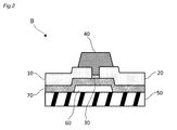
- FIG. 2 is a schematic diagram of a semiconductor device B according to the second embodiment.
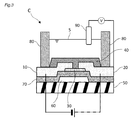
- FIG. 3 is a schematic diagram of a pH sensor C including the semiconductor device A according to the first embodiment.
- FIG. 4 is a diagram showing an example of a method for manufacturing the semiconductor device A according to the first embodiment.
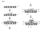
- FIG. 5 is a diagram showing an example of a method for manufacturing the semiconductor device B according to the second embodiment.
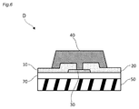
- FIG. 6 is a schematic sectional view of the semiconductor device D of the first embodiment.
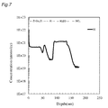
- FIG. 7 is a graph of SIMS measurement results of Example 1.
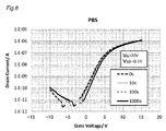
- FIG. 8 is a graph of the PBS test of Example 1.
- FIG. 9 is a graph of the NBS test of Example 1.
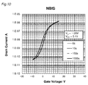
- FIG. 10 is a graph of the NBIS test of Example 1.
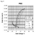
- FIG. 11 is a graph of the PBS test of Comparative Example 1.
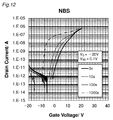
- FIG. 12 is a graph of the NBS test of Comparative Example 1.
- this embodiment modes for carrying out the present invention (hereinafter, simply referred to as “this embodiment”) will be described in detail.
- the following embodiments are examples for explaining the present invention, and are not intended to limit the present invention to the following contents.
- the positional relationship such as up, down, left, and right is based on the positional relationship shown in the drawings unless otherwise specified.
- the dimensional ratios in the drawings are not limited to the illustrated ratios.
- FIG. 1 is a schematic diagram of a semiconductor device A according to the first embodiment.
- the semiconductor device A according to the first embodiment is a bottom gate/top contact (BGTC) type semiconductor device.
- the semiconductor device A covers the first electrode 10, the second electrode 20, the semiconductor layer 30 in contact with the first electrode 10 and the second electrode 20, and at least a part of the surface of the semiconductor layer 30.
- a protective layer 40, and the protective layer 40 is a semiconductor device including a spinel-type oxide.
- the semiconductor device A has the substrate 50, the third electrode 60 formed on the substrate 50, and the insulating layer 70 on the surface of the substrate 50 on the side where the third electrode 60 is formed.
- the first electrode 10 is a source electrode
- the second electrode 20 is a drain electrode
- the third electrode 60 is a gate electrode.
- the semiconductor device A uses an oxide having a spinel type crystal structure (hereinafter, may be abbreviated as “spinel type oxide”) as the protective layer 40, so that the film forming temperature is low and the film forming rate is also high. It has the advantage of being quick and free of impurities. In addition, there is an advantage that even when a flexible substrate is used, it can be easily manufactured.
- spinel type oxide oxide having a spinel type crystal structure
- a metal oxide film such as silicon oxide or aluminum oxide has been generally used as a protective layer, but these have many problems such as film forming temperature and film forming speed.
- CVD method chemical vapor deposition method
- the film forming temperature is high, a large-scale CVD film forming apparatus is required, and impurities such as hydrogen and carbon derived from the material gas.
- impurities such as hydrogen and carbon derived from the material gas.
- RF radio frequency
- the semiconductor device A can solve these problems at once by using the spinel type oxide as the protective layer 40.
- the spinel oxide can be formed relatively easily and efficiently as compared with the above-described metal oxide film and the like.
- the protective layer 40 of the semiconductor device A uses a stable spinel type oxide, it can exhibit a passivation effect as good as or better than a conventional protective layer using a metal oxide film. Therefore, the semiconductor device A is also excellent in semiconductor characteristics.
- the configuration of the semiconductor device A will be described below.
- the source electrode is not particularly limited, and a known electrode can be used. Specific examples include single layers of Mo, W, Al, Cu, Au, Cu-Al alloys, Al-Si alloys, Mo-W alloys, Ni-P alloys, etc., and laminates thereof.
- the drain electrode is not particularly limited, and a known electrode can be adopted. Specific examples include single layers of Mo, W, Al, Cu, Au, Cu-Al alloys, Al-Si alloys, Mo-W alloys, Ni-P alloys, etc., and laminates thereof.
- the semiconductor layer 30 is formed in contact with the first electrode 10 and the second electrode 20.
- the semiconductor layer 30 is not particularly limited, and a known material can be used. Specific examples include inorganic oxide semiconductors containing zinc oxide (ZnO), In, Ga, and Zn, IGZTO in which tin is mixed with IGZO, amorphous silicon, low-temperature polysilicon, and the like. Among these, an oxide containing In, Ga, and Zn, which has excellent semiconductor characteristics, is preferable, and among these, InGaZnO 4 (IGZO) is more preferable.
- the semiconductor layer 30 is preferably doped with a carrier element from the viewpoint of further improving semiconductor characteristics.
- the carrier element is not particularly limited, and a known element in the doping process can be adopted. Specific examples include hydrogen, monovalent metal, divalent metal, trivalent metal and the like. Among these, in the present embodiment, the semiconductor layer 30 is more preferably doped with hydrogen.
- the protective layer 40 may be a spinel type oxide, for example, a spinel type oxide containing zinc and gallium (for example, spinel type ZnGa 2 O 4 or the like), a spinel type oxide containing zinc and indium (for example, spinel type ZnIn 2 O 4 etc.), spinel type oxide containing zinc and aluminum (eg spinel type ZnAl 2 O 4 etc.), spinel type oxide containing magnesium and aluminum (eg spinel type). MgAl 2 O 4 etc.) and the like.
- a spinel type oxide containing zinc and gallium is preferable, and a spinel type ZnGa 2 O 4 is more preferable, from the viewpoint of crystallization at a relatively low temperature.
- the protective layer 40 may be hydrogen-free in this embodiment. That is, as the protective layer, a layer that is not doped with hydrogen or a layer that does not substantially contain hydrogen can be preferably used.
- the term "substantially free from” as used herein means that the component is not positively added, and does not exclude inevitable inclusion or mixing.
- the presence of hydrogen in the protective layer 40 may cause a defect that it also enters the semiconductor layer 30 as an impurity. For example, if impurities such as hydrogen are present, they diffuse into the semiconductor and the V TH (threshold voltage) shift amount increases.
- impurities such as hydrogen
- the hydrogen content of the protective layer 40 is preferably 1 ⁇ 10 21 atm/cc or less, and more preferably 1 ⁇ 10 18 atm/cc or less. This hydrogen content can be measured by the secondary ion mass spectrometry (SIMS) described in Examples described later.
- the protective layer 40 can also function as a passivation layer.
- the passivation layer shields the semiconductor layer 30 from the environment, and can protect the semiconductor layer 30 from moisture and metal ions.
- the thickness of the protective layer 40 may be 40 nm or more.
- the upper limit of the film thickness is not particularly limited, but may be 1 ⁇ m.
- the material of the substrate 50 is not particularly limited, and a known material can be used. Specific examples include glass, resin, silicon, metals, alloys, and foils thereof. Among these, one selected from the group consisting of glass, resin, silicon, and combinations thereof is preferable.
- the resin for example, polyacrylate, polycarbonate, polyurethane, polystyrene, cellulose polymer, polyolefin, polyamide, polyimide, polyester, polyphenylene, polyethylene, polyethylene terephthalate, polypropylene, ethylene vinyl copolymer, polyvinyl chloride and the like can be used.
- the substrate 50 may have flexibility.
- the formation of the protective layer 40 does not need to be performed by a CVD method, which has strong restrictions on film forming conditions, and there are few restrictions on the method of forming the spinel type oxide as the protective layer 40. The restrictions of can be relaxed. Therefore, even when a flexible material is used for the substrate 50, the protective layer 40 can be preferably formed.
- the flexible substrate include the above-mentioned resin materials and the like.
- the substrate 50 is a flexible film substrate (sometimes called a “sheet substrate”), a roll-to-roll method of continuously forming a film in a roll shape, The roll-to-sheet method can be adopted, and high efficiency, simplification, and improvement in yield of the manufacturing process can be expected.
- Roll-to-roll method refers to a method in which a roll-shaped film substrate is unwound, continuously formed into a film, and then rewound into a roll.
- the roll-to-sheet method refers to a method in which a roll-shaped film substrate is unwound to continuously form a film, and this is cut into a sheet.
- the third electrode 60 is a gate electrode.
- the third electrode 60 is not particularly limited, and a known electrode can be adopted. Specific examples include single layers of Mo, W, Al, Cu, Au, Cu-Al alloys, Al-Si alloys, Mo-W alloys, Ni-P alloys, etc., and laminates thereof.
- the method for forming the third electrode 60, which is the gate electrode, is not particularly limited, and a suitable method can be adopted as appropriate in consideration of the material of the substrate 50 and the gate electrode.
- the insulating layer 70 is not particularly limited, and a known material can be used. Specific examples include, for example, inorganic materials such as SiO 2 , Si 3 N 4 , SiON, Al 2 O 3 , Ta 2 O 5 , and HfO 2 , and photocurable resins and thermosetting resins.
- a transistor having the first electrode 10, the second electrode 20, and the third electrode 60 as a source electrode, a drain electrode, and a gate electrode may be configured.
- the third electrode 60 (gate electrode) may not be provided.
- the substrate 50 and the insulating layer 70 may not be provided.
- the semiconductor device according to this embodiment is not limited to the configuration shown in FIG. 1 and various configurations can be adopted.
- FIG. 2 is a schematic diagram of a semiconductor device B according to the second embodiment.
- the semiconductor device B according to the second embodiment is a bottom gate/bottom contact (BGBC) type semiconductor device.
- the protective layer 40 covers at least a part of the surface of the semiconductor layer 30.
- each member constituting the semiconductor device B the same members as those of the semiconductor device A described above may be the same as those of the semiconductor device A unless otherwise specified.
- the structure of the semiconductor device is not particularly limited, and the bottom gate/top contact type (see FIG. 1), the bottom gate/bottom contact type (see FIG. 2), the top gate/top contact type, the top gate. -A bottom contact type structure can be adopted.
- the semiconductor devices A and B described so far have excellent semiconductor characteristics such as electronic conductivity, and also have chemical resistance such as acid resistance and base resistance by having the protective layer 40.
- the semiconductor devices A and B are made into devices, it is expected that the wiring patterns will be finer and finer, and the weight of the devices can be reduced. Therefore, the semiconductor device according to the present embodiment can be suitably used as various sensors such as a pH sensor and a biosensor as well as parts such as a TFT liquid crystal and an organic EL. Some of them will be described below.
- FIG. 3 is a schematic diagram of a pH sensor C including the semiconductor device A according to the first embodiment.
- the pH sensor C is, for example, a pH sensor (Ion Sensitive-FET; ion sensitive field effect transistor) using the semiconductor device A according to the present embodiment.
- the pH sensor C has a semiconductor device A, a pool wall 80 made of silicon rubber provided on the semiconductor device A, and a reference electrode 90. Then, the solution S to be measured (for example, hydrochloric acid in the case of an acidic solution, sodium hydroxide solution in the case of an alkaline solution, etc.) is filled in the pool constituted by the pool wall 80, and the reference electrode 90 and the electrode are separated from each other. Measure the potential difference. Since the pH of the solution S depends on the amount of protons in the solution, the measurement principle of the pH sensor is to electrically measure the amount of protons in the solution and calculate the pH value based on the measured amount of protons.
- the solution S to be measured for example, hydrochloric acid in the case of an acidic solution, sodium hydroxide solution in the case of an alkaline solution, etc.
- the semiconductor device A according to this embodiment can have high stability against a strong acid or a strong base. Therefore, the pH sensor C using this has high stability in a wide pH range such as pH 1 to 14, and quick and accurate measurement is possible even when the target material is a strong acid or strong base.
- the semiconductor device A is used as an example of the pH sensor, but it goes without saying that the semiconductor device B may be used.
- the semiconductor devices A and B according to this embodiment can also be used as a biosensor (also referred to as a biosensor chip).
- the biosensor is a chemical sensor utilizing a molecular recognition mechanism of biological origin, and is used as a chemical recognition element for pH change in the living body, redox reaction and the like.
- the semiconductor devices A and B according to the present embodiment have high stability in a wide pH range, it is possible to provide a biosensor capable of accurate sensing even if the measurement target is strongly acidic or strongly basic. it can.
- a biosensor can be used in which a semiconductor surface is modified with a specific antibody and the amount of protons when a detection target such as DNA specific thereto is adsorbed is measured.
- FIG. 4 is a diagram showing an example of a method for manufacturing the semiconductor device A according to the first embodiment.
- the manufacturing method shown in FIG. 4 is a method of manufacturing the bottom gate/top contact type (see FIG. 1) semiconductor device A.
- a step of forming the semiconductor layer 30 on the substrate 50, a step of forming a conductive layer (not shown) on the substrate 50, and etching the conductive layer in a predetermined pattern are performed.
- the step of forming the protective layer 40 by performing sputtering at a film forming temperature of 200° C. or lower so as to cover at least a part of the surface of the semiconductor layer 30. And, it does.
- each step will be described in detail.
- the third electrode 60 is formed on the surface of the substrate 50.
- the third electrode 60 corresponds to the above-mentioned gate electrode.
- the method of forming the third electrode 60 on the surface of the substrate 50 is not particularly limited, and a suitable method can be adopted as appropriate in consideration of the material of the substrate 50 and the electrodes.
- the insulating layer 70 is formed on the surface of the substrate 50 on the side where the third electrode 60 is formed, and the third electrode 60 is covered with the insulating layer 70.
- the method for forming the insulating layer 70 is not particularly limited, and a suitable method can be adopted as appropriate in consideration of the material of the substrate 50, the third electrode 60, the insulating layer 70, and the like.
- the semiconductor layer 30 is formed on the surface of the insulating layer 70.
- the semiconductor layer 30 is preferably formed by a sputtering method. In this case, it can be formed using a sputtering apparatus, and the predetermined semiconductor layer 30 may be formed using a plurality of cathodes.
- sputtering unitary simultaneous sputtering targeting one kind of material may be adopted, or co-sputtering targeting plural kinds of materials may be adopted.
- the semiconductor layer 30 is formed of an IGZO thin film.
- an oxide sintered body of InGaZnO 4 may be used as a target (one-way simultaneous sputtering), and by using three kinds of In 2 O 3 , Ga 2 O 3 , and ZnO simultaneously, the composition ratio can be increased.
- the IGZO film may be tilted and controlled to form an IGZO film having a desired composition (multi-source simultaneous sputtering, co-sputtering).
- n-type semiconductor material it is possible to fabricate by element doping and oxygen deficiency in the film.
- the element from which the n-type semiconductor is obtained is not particularly limited, but examples thereof include Al, In, Sn, Sb, and Ta.
- the method for generating oxygen deficiency is not particularly limited, and a known method can be adopted.
- an anaerobic atmosphere or a reducing gas atmosphere such as hydrogen or steam.
- the film formation temperature of the semiconductor layer 30 is preferably 190° C. or higher from the viewpoint of improving the crystallinity of the semiconductor layer 30.
- the upper limit of the film forming temperature is preferably 400°C.
- a step of forming the first electrode 10 and the second electrode 20 by forming a conductive layer (not shown) having conductivity on the semiconductor layer 30 and etching the conductive layer so as to correspond to a predetermined pattern. I do.
- the first electrode 10 is a source electrode and the second electrode 20 is a drain electrode.
- a usual photolithography process can be used as a method for forming the first electrode 10 and the second electrode 20 .
- a resist layer is formed on the conductive layer, and the resist layer is exposed to a predetermined pattern of light and developed.
- the first electrode 10 and the second electrode 20 can be formed by etching the conductive layer exposed from the opening of the resist layer.
- a positive type material or a negative type material may be used as the resist layer.
- the etching solution is preferably an acidic solution. Since the resist material used in the usual photolithography process is soluble in alkalinity, it is possible to preferably etch the conductive layer without dissolving the resist layer by using an acidic solution.
- an etch stop layer may be formed on the semiconductor layer 30 before the conductive layer is formed. This can prevent the semiconductor layer 30 from being deteriorated due to contact with the etching solution when the conductive layer is etched.
- the semiconductor device A can be obtained by forming the protective layer 40 on the first electrode 10 and the second electrode 20 formed in the fourth step.
- the protective layer 40 By forming the protective layer 40 on the outermost surface of the substrate 50, the inside of the semiconductor device A can be protected from moisture and metal ions in the outside world.
- the film forming temperature was required to be 300°C or higher.
- the spinel oxide used has a low film forming temperature and a high film forming rate, a semiconductor device can be manufactured easily and efficiently.
- the film formation temperature of the protective layer 40 is 200° C. or lower, preferably 190° C. or lower.
- the protective layer 40 is formed of a spinel type oxide containing zinc (Zn) and gallium (Ga) will be described.
- the protective layer 40 can be expected to exhibit strong resistance to a strong acid or a strong base.
- the protective layer 40 made of spinel-type gallium zinc oxide can be formed by performing co-sputtering using gallium zinc oxide and zinc oxide as targets.
- a method of co-sputtering using gallium oxide and zinc oxide as a target, or a method of co-sputtering using gallium and zinc as a target and oxidizing with a reactive gas during film formation may be used.
- a method of sputtering using a mixture of zinc oxide and gallium oxide as a target, or sputtering using a mixture of zinc and gallium as a target and oxidizing with a reactive gas during film formation The method of doing may be used.
- the semiconductor device A thus obtained may be subjected to other steps as necessary so as to have a desired device configuration.
- a pretreatment step before forming each part a surface polishing step after forming each part, a dicing step, a mounting step on a lead frame, an assembling step for packaging after circuit formation, a wire bonding step, A mold encapsulation process or the like can be appropriately adopted.
- FIG. 5 is a diagram showing an example of a method of manufacturing the semiconductor device B according to the second embodiment.
- the manufacturing method shown in FIG. 5 is a method of manufacturing the bottom gate/bottom contact type (see FIG. 2) semiconductor device B.
- the semiconductor layer 30 and the protective layer 40 are continuously formed.
- each step will be described in detail.
- the third electrode 60 is formed on the surface of the substrate 50.
- the third electrode 60 corresponds to the above-mentioned gate electrode.
- the method of forming the third electrode 60 on the surface of the substrate 50 is not particularly limited, and a suitable method can be adopted as appropriate in consideration of the material of the substrate 50 and the electrodes.
- the insulating layer 70 is formed on the surface of the substrate 50 on the side where the third electrode 60 is formed, and the third electrode 60 is covered with the insulating layer 70.
- the method for forming the insulating layer 70 is not particularly limited, and a suitable method can be adopted as appropriate in consideration of the material of the substrate 50, the third electrode 60, the insulating layer 70, and the like.
- a conductive layer (not shown) having conductivity is formed on the surface of the insulating layer 70, and the conductive layer is etched in accordance with a predetermined pattern to etch the first electrode 10 and the second electrode 20. Is performed.
- the first electrode 10 is a source electrode and the second electrode 20 is a drain electrode.
- a usual photolithography process can be used as a method for forming the first electrode 10 and the second electrode 20.
- a resist layer is formed on the conductive layer, and the resist layer is exposed to a predetermined pattern of light and developed.
- the first electrode 10 and the second electrode 20 can be formed by etching the conductive layer exposed from the opening of the resist layer.
- a positive type material or a negative type material may be used as the resist layer.
- the etching solution is preferably an acidic solution. Since the resist material used in the usual photolithography process is soluble in alkalinity, it is possible to preferably etch the conductive layer without dissolving the resist layer by using an acidic solution.
- the semiconductor layer 30 is formed on the surface of the insulating layer 70 so as to contact the first electrode 10 and the second electrode 20. Then, a protective layer 40 is formed so as to cover the semiconductor layer 30.
- the semiconductor layer 30 and the protective layer 40 are preferably formed by a sputtering method.
- it can be formed using a sputtering apparatus, and it is preferable to form the predetermined semiconductor layer 30 and protective layer 40 using a plurality of cathodes.
- the semiconductor layer 30 and the protective layer 40 by the same forming method (for example, the sputtering method), it becomes easy to continuously form the semiconductor layer 30 and the protective layer 40.
- single-unit simultaneous sputtering targeting one kind of material may be adopted, or co-sputtering targeting plural kinds of materials may be adopted.
- the semiconductor layer 30 is formed of an IGZO thin film.
- an oxide sintered body of InGaZnO 4 may be used as a target (one-way simultaneous sputtering), and by using three kinds of In 2 O 3 , Ga 2 O 3 , and ZnO simultaneously, the composition ratio can be increased.
- the IGZO film may be tilted and controlled to form an IGZO film having a desired composition (multi-source simultaneous sputtering, co-sputtering).
- n-type semiconductor material it is possible to fabricate by element doping and oxygen deficiency in the film.
- the element from which the n-type semiconductor is obtained is not particularly limited, but examples thereof include Al, In, Sn, Sb, and Ta.
- the method for generating oxygen deficiency is not particularly limited, and a known method can be adopted.
- an anaerobic atmosphere or a reducing gas atmosphere such as hydrogen.
- the film forming temperature of the semiconductor layer 30 is preferably 105° C. or higher, and more preferably 150° C. or higher, from the viewpoint of improving the film density of the semiconductor layer 30.
- the upper limit of the film forming temperature is preferably 300°C.
- the protective layer 40 By forming the protective layer 40 on the outermost surface of the substrate 50, the inside of the semiconductor device B can be protected from moisture and metal ions in the outside world.
- the film forming temperature was required to be 300°C or higher.
- the film forming temperature is low and the film forming rate is high, the semiconductor device can be manufactured simply and efficiently.
- the film formation temperature of the protective layer 40 is 200° C. or lower, preferably 190° C. or lower.
- the protective layer 40 is formed of a spinel type oxide containing zinc (Zn) and gallium (Ga) will be described.
- the protective layer 40 can be expected to exhibit strong resistance to a strong acid or a strong base.
- the protective layer 40 made of spinel-type gallium zinc oxide can be formed by performing co-sputtering using gallium zinc oxide and zinc oxide as targets.
- a method of co-sputtering using gallium oxide and zinc oxide as a target, or a method of co-sputtering using gallium and zinc as a target and oxidizing with a reactive gas during film formation may be used.
- a method of sputtering using a mixture of zinc oxide and gallium oxide as a target, or a method of sputtering using a mixture of zinc and gallium as a target and oxidizing with a reactive gas during film formation The method of doing may be used.
- both the semiconductor layer 30 and the protective layer 40 be formed by a sputtering method.
- the semiconductor layer 30 is made of IGZO and the protective layer 40 is spinel-type gallium zinc oxide
- the target of the sputtering method can be commonly used, and therefore, after the semiconductor layer 30 is formed, it can be directly used in the same device.
- the protective layer 40 can be continuously formed. As a result, simple and continuous production is possible without making the device configuration large.
- the semiconductor device B thus obtained may be subjected to other steps as necessary so as to have a desired device configuration.
- a pretreatment step before forming each part a surface polishing step after forming each part, a dicing step, a mounting step on a lead frame, an assembling step for packaging after circuit formation, a wire bonding step, A mold encapsulation process or the like can be appropriately adopted.
- FIG. 6 is a schematic sectional view of the semiconductor device D of the first embodiment.
- a high-conductivity p-type silicon substrate in which a 200-nm thermal oxide film (SiO 2 ) was formed on a p-type doped (boron-doped) silicon wafer was prepared.
- An ⁇ -IGZO thin film was formed on this substrate.
- the ⁇ -IGZO thin film was formed by an RF sputtering method using an InGaZnO target having an In:Ga:Zn atomic concentration of 1:1:1.
- the substrate temperature during film formation was 105°C.
- an Al electrode (having a film thickness of 80 nm) to be a source/drain electrode was formed by a vacuum vapor deposition method using a metal mask.
- the source/drain electrodes were formed using a resistance heating type vacuum vapor deposition apparatus.
- a spinel-type ZnGa 2 O 4 thin film was formed as a protective layer so as to cover the above-mentioned ⁇ -IGZO thin film, and this was used as a passivation film.
- the ZnGa 2 O 4 thin film was formed by co-sputtering in which the ZnO target and the Ga 2 O 3 target were simultaneously sputtered using the same sputtering apparatus used for forming the ⁇ -IGZO thin film.
- ZnGa 2 O 4 has a spinel type crystal structure.
- the semiconductor device D having the structure shown in FIG. 6 was manufactured.
- FIG. 7 is a graph of SIMS measurement results of Example 1.
- the structure of the obtained semiconductor device was confirmed by ⁇ -2 ⁇ measurement by XRD (X-ray diffraction method) and secondary ion mass spectrometry (SIMS). The result is shown in FIG. 7. Thus, it was confirmed that the ZnGa 2 O 4 thin film was a spinel type ZnGa 2 O 4 thin film, and that the hydrogen content of the passivation film was 1 ⁇ 10 21 atm/cc or less.
- Example 1 A semiconductor device was manufactured in the same manner as in Example 1 except that the passivation film was not formed.
- TFT thin film transistor
- 4200-SCS semiconductor parameter analyzer 4200-SCS, manufactured by KEITHLEY
- the following bias stress resistance was evaluated using the gate electrode as the Si substrate and the source/drain electrodes as the Al electrodes.
- PBS +20 V Positive Bias Stress +20 V was applied to the gate electrode for 0 seconds, 10 seconds, 100 seconds, and 1000 seconds, and the transfer characteristics of each were measured.
- NBS Negative Bias Stress
- Negative Bias Illumination Stress (NBIS) -20 V was applied to the gate electrode for 0 seconds, 10 seconds, 100 seconds, and 1000 seconds, and white light (irradiation condition: 1000 lux) was irradiated to measure the transfer characteristics of each.
- FIG. 8 is a graph of the PBS test of Example 1
- FIG. 9 is a graph of the NBS test of Example 1
- FIG. 10 is a graph of the NBIS test of Example 1.
- the semiconductor device of Example 1 had a small shift over 0 seconds to 1000 seconds and had excellent mobility as a transistor. It was also confirmed that the semiconductor device of Example 1 can be manufactured by a manufacturing method having a low film forming temperature and a high film forming rate, and has excellent semiconductor characteristics because the content of impurities is small.
- FIG. 11 is a graph of the PBS test of Comparative Example 1
- FIG. 12 is a graph of the NBS test of Comparative Example 1.
Landscapes
- Life Sciences & Earth Sciences (AREA)
- Health & Medical Sciences (AREA)
- Chemical & Material Sciences (AREA)
- Physics & Mathematics (AREA)
- Molecular Biology (AREA)
- General Physics & Mathematics (AREA)
- Electrochemistry (AREA)
- Analytical Chemistry (AREA)
- Biochemistry (AREA)
- General Health & Medical Sciences (AREA)
- Chemical Kinetics & Catalysis (AREA)
- Immunology (AREA)
- Pathology (AREA)
- Microelectronics & Electronic Packaging (AREA)
- Engineering & Computer Science (AREA)
- Spectroscopy & Molecular Physics (AREA)
- Thin Film Transistor (AREA)
- Optics & Photonics (AREA)
- Formation Of Insulating Films (AREA)
- Physical Deposition Of Substances That Are Components Of Semiconductor Devices (AREA)
- Bipolar Transistors (AREA)
- Investigating Or Analyzing Materials By The Use Of Electric Means (AREA)
- Measurement Of Length, Angles, Or The Like Using Electric Or Magnetic Means (AREA)
Abstract
La présente invention concerne un dispositif à semi-conducteur A qui comprend une première électrode (10), une seconde électrode (20), une couche semi-conductrice (30) qui est en contact avec la première électrode (10) et la seconde électrode (20), et une couche de protection (40) qui recouvre au moins une partie de la surface de la couche semi-conductrice (30), et qui est conçue de telle sorte que la couche de protection (40) contient un oxyde de spinelle.
Priority Applications (4)
| Application Number | Priority Date | Filing Date | Title |
|---|---|---|---|
| JP2021501397A JP7147953B2 (ja) | 2019-02-25 | 2019-02-25 | 半導体装置、pHセンサ及びバイオセンサ並びに半導体装置の製造方法 |
| PCT/JP2019/007093 WO2020174540A1 (fr) | 2019-02-25 | 2019-02-25 | DISPOSITIF À SEMI-CONDUCTEUR, CAPTEUR DE pH, BIOCAPTEUR ET PROCÉDÉ DE PRODUCTION DE DISPOSITIF À SEMI-CONDUCTEUR |
| TW108140248A TWI815991B (zh) | 2019-02-25 | 2019-11-06 | 半導體裝置、pH感測器及生物感測器以及半導體裝置的製造方法 |
| US17/411,805 US12596093B2 (en) | 2019-02-25 | 2021-08-25 | Organic semiconductor device with protective spinel oxide layer |
Applications Claiming Priority (1)
| Application Number | Priority Date | Filing Date | Title |
|---|---|---|---|
| PCT/JP2019/007093 WO2020174540A1 (fr) | 2019-02-25 | 2019-02-25 | DISPOSITIF À SEMI-CONDUCTEUR, CAPTEUR DE pH, BIOCAPTEUR ET PROCÉDÉ DE PRODUCTION DE DISPOSITIF À SEMI-CONDUCTEUR |
Related Child Applications (1)
| Application Number | Title | Priority Date | Filing Date |
|---|---|---|---|
| US17/411,805 Continuation US12596093B2 (en) | 2019-02-25 | 2021-08-25 | Organic semiconductor device with protective spinel oxide layer |
Publications (1)
| Publication Number | Publication Date |
|---|---|
| WO2020174540A1 true WO2020174540A1 (fr) | 2020-09-03 |
Family
ID=72240008
Family Applications (1)
| Application Number | Title | Priority Date | Filing Date |
|---|---|---|---|
| PCT/JP2019/007093 Ceased WO2020174540A1 (fr) | 2019-02-25 | 2019-02-25 | DISPOSITIF À SEMI-CONDUCTEUR, CAPTEUR DE pH, BIOCAPTEUR ET PROCÉDÉ DE PRODUCTION DE DISPOSITIF À SEMI-CONDUCTEUR |
Country Status (4)
| Country | Link |
|---|---|
| US (1) | US12596093B2 (fr) |
| JP (1) | JP7147953B2 (fr) |
| TW (1) | TWI815991B (fr) |
| WO (1) | WO2020174540A1 (fr) |
Cited By (2)
| Publication number | Priority date | Publication date | Assignee | Title |
|---|---|---|---|---|
| WO2022249872A1 (fr) * | 2021-05-26 | 2022-12-01 | 株式会社ニコン | APPAREIL À SEMI-CONDUCTEUR, DISPOSITIF ÉLECTRONIQUE, CAPTEUR DE pH, BIOCAPTEUR, PROCÉDÉ DE PRODUCTION POUR APPAREIL À SEMI-CONDUCTEUR, ET PROCÉDÉ DE PRODUCTION POUR DISPOSITIF ÉLECTRONIQUE |
| WO2025215780A1 (fr) * | 2024-04-11 | 2025-10-16 | 株式会社ニコン | Dispositif à semi-conducteur, dispositif électronique, capteur de ph, biocapteur et procédé de fabrication de dispositif à semi-conducteur |
Citations (4)
| Publication number | Priority date | Publication date | Assignee | Title |
|---|---|---|---|---|
| JP2010056540A (ja) * | 2008-07-31 | 2010-03-11 | Semiconductor Energy Lab Co Ltd | 半導体装置およびその作製方法 |
| JP2016074580A (ja) * | 2014-02-21 | 2016-05-12 | 株式会社半導体エネルギー研究所 | 半導体膜、トランジスタ及び半導体装置、並びに表示装置、電子機器 |
| JP2017118106A (ja) * | 2015-12-18 | 2017-06-29 | 株式会社半導体エネルギー研究所 | 半導体装置 |
| WO2018025647A1 (fr) * | 2016-08-03 | 2018-02-08 | 株式会社ニコン | Dispositif à semi-conducteur, capteur de ph, biocapteur, et procédé de production de dispositif à semi-conducteur |
Family Cites Families (20)
| Publication number | Priority date | Publication date | Assignee | Title |
|---|---|---|---|---|
| DE3688489T2 (de) * | 1985-08-29 | 1993-09-16 | Matsushita Electric Ind Co Ltd | Einen feldeffekttransistor benutzender fuehler und dessen herstellungsverfahren. |
| EP1815530B1 (fr) * | 2004-11-10 | 2021-02-17 | Canon Kabushiki Kaisha | Transistor a effet de champ utilisant un oxyde amorphe |
| TWI302197B (en) * | 2006-01-04 | 2008-10-21 | Univ Nat Yunlin Sci & Tech | Reference ph sensor, the preparation and application thereof |
| GB0811962D0 (en) * | 2008-06-30 | 2008-07-30 | Imp Innovations Ltd | Improved fabrication method for thin-film field-effect transistors |
| KR100963104B1 (ko) * | 2008-07-08 | 2010-06-14 | 삼성모바일디스플레이주식회사 | 박막 트랜지스터, 그의 제조 방법 및 박막 트랜지스터를구비하는 평판 표시 장치 |
| WO2011048959A1 (fr) * | 2009-10-21 | 2011-04-28 | Semiconductor Energy Laboratory Co., Ltd. | Dispositif à semi-conducteur et son procédé de fabrication |
| WO2011062043A1 (fr) * | 2009-11-20 | 2011-05-26 | Semiconductor Energy Laboratory Co., Ltd. | Procédé de fabrication de dispositif à semi-conducteur |
| CN105206514B (zh) * | 2009-11-28 | 2018-04-10 | 株式会社半导体能源研究所 | 层叠的氧化物材料、半导体器件、以及用于制造该半导体器件的方法 |
| KR101273831B1 (ko) * | 2009-12-09 | 2013-06-11 | 샤프 가부시키가이샤 | 반도체 장치 및 그 제조 방법 |
| US8698152B2 (en) * | 2010-05-24 | 2014-04-15 | Sharp Kabushiki Kaisha | Display panel and thin film transistor substrate |
| US8552425B2 (en) * | 2010-06-18 | 2013-10-08 | Semiconductor Energy Laboratory Co., Ltd. | Semiconductor device |
| US9064965B2 (en) * | 2012-02-24 | 2015-06-23 | Rutgers, The State University Of New Jersey | Zinc oxide-based thin film transistor biosensors with high sensitivity and selectivity |
| US9048323B2 (en) * | 2012-04-30 | 2015-06-02 | Semiconductor Energy Laboratory Co., Ltd. | Semiconductor device |
| KR101980195B1 (ko) * | 2012-05-16 | 2019-05-21 | 삼성전자주식회사 | 황 도핑 징크옥시 나이트라이드 채널층을 가진 트랜지스터 및 그 제조방법 |
| US20150380561A1 (en) * | 2013-03-01 | 2015-12-31 | Applied Materials, Inc. | Metal oxide tft stability improvement |
| CN103762244A (zh) * | 2013-11-29 | 2014-04-30 | 深圳市华星光电技术有限公司 | 薄膜晶体管及其制造方法、薄膜晶体管阵列基板及液晶面板 |
| JP6372848B2 (ja) * | 2014-03-28 | 2018-08-15 | Tianma Japan株式会社 | Tftイオンセンサ並びにこれを用いた測定方法及びtftイオンセンサ機器 |
| CN105140234B (zh) * | 2015-07-28 | 2018-03-27 | 京东方科技集团股份有限公司 | 阵列基板及其制造方法、显示装置 |
| US10482987B2 (en) * | 2016-04-21 | 2019-11-19 | Tdk Corporation | Magnetic wall utilization spin MOSFET and magnetic wall utilization analog memory |
| US11442695B2 (en) * | 2017-12-28 | 2022-09-13 | Tdk Corporation | Product-sum operation device, neuromorphic device, and method for determining malfunction in product-sum operation device |
-
2019
- 2019-02-25 WO PCT/JP2019/007093 patent/WO2020174540A1/fr not_active Ceased
- 2019-02-25 JP JP2021501397A patent/JP7147953B2/ja active Active
- 2019-11-06 TW TW108140248A patent/TWI815991B/zh active
-
2021
- 2021-08-25 US US17/411,805 patent/US12596093B2/en active Active
Patent Citations (4)
| Publication number | Priority date | Publication date | Assignee | Title |
|---|---|---|---|---|
| JP2010056540A (ja) * | 2008-07-31 | 2010-03-11 | Semiconductor Energy Lab Co Ltd | 半導体装置およびその作製方法 |
| JP2016074580A (ja) * | 2014-02-21 | 2016-05-12 | 株式会社半導体エネルギー研究所 | 半導体膜、トランジスタ及び半導体装置、並びに表示装置、電子機器 |
| JP2017118106A (ja) * | 2015-12-18 | 2017-06-29 | 株式会社半導体エネルギー研究所 | 半導体装置 |
| WO2018025647A1 (fr) * | 2016-08-03 | 2018-02-08 | 株式会社ニコン | Dispositif à semi-conducteur, capteur de ph, biocapteur, et procédé de production de dispositif à semi-conducteur |
Cited By (6)
| Publication number | Priority date | Publication date | Assignee | Title |
|---|---|---|---|---|
| WO2022249872A1 (fr) * | 2021-05-26 | 2022-12-01 | 株式会社ニコン | APPAREIL À SEMI-CONDUCTEUR, DISPOSITIF ÉLECTRONIQUE, CAPTEUR DE pH, BIOCAPTEUR, PROCÉDÉ DE PRODUCTION POUR APPAREIL À SEMI-CONDUCTEUR, ET PROCÉDÉ DE PRODUCTION POUR DISPOSITIF ÉLECTRONIQUE |
| JPWO2022249872A1 (fr) * | 2021-05-26 | 2022-12-01 | ||
| KR20230169355A (ko) * | 2021-05-26 | 2023-12-15 | 가부시키가이샤 니콘 | 반도체 장치, 전자 디바이스, pH 센서, 바이오 센서, 반도체 장치의 제조 방법, 및 전자 디바이스의 제조 방법 |
| JP7632606B2 (ja) | 2021-05-26 | 2025-02-19 | 株式会社ニコン | 半導体装置、電子デバイス、pHセンサ、バイオセンサ、半導体装置の製造方法、及び電子デバイスの製造方法 |
| KR102813570B1 (ko) * | 2021-05-26 | 2025-05-27 | 가부시키가이샤 니콘 | 반도체 장치, 전자 디바이스, pH 센서, 바이오 센서, 반도체 장치의 제조 방법, 및 전자 디바이스의 제조 방법 |
| WO2025215780A1 (fr) * | 2024-04-11 | 2025-10-16 | 株式会社ニコン | Dispositif à semi-conducteur, dispositif électronique, capteur de ph, biocapteur et procédé de fabrication de dispositif à semi-conducteur |
Also Published As
| Publication number | Publication date |
|---|---|
| JP7147953B2 (ja) | 2022-10-05 |
| JPWO2020174540A1 (ja) | 2021-12-02 |
| US20220034837A1 (en) | 2022-02-03 |
| TWI815991B (zh) | 2023-09-21 |
| US12596093B2 (en) | 2026-04-07 |
| TW202102697A (zh) | 2021-01-16 |
Similar Documents
| Publication | Publication Date | Title |
|---|---|---|
| JP7285302B2 (ja) | 半導体装置 | |
| Liang et al. | Recent progress of deep ultraviolet photodetectors using amorphous gallium oxide thin films | |
| Park et al. | 42.3: Transparent ZnO thin film transistor for the application of high aperture ratio bottom emission AM‐OLED display | |
| TWI618252B (zh) | 半導體裝置 | |
| TWI427795B (zh) | Field-effect transistor and field-effect transistor manufacturing method | |
| KR101654663B1 (ko) | 전자소자와 그 제조방법, 표시장치, 및 센서 | |
| US20240201125A1 (en) | SEMICONDUCTOR APPARATUS, ELECTRONIC DEVICE, pH SENSOR, BIOSENSOR, PRODUCTION METHOD FOR SEMICONDUCTOR APPARATUS, AND PRODUCTION METHOD FOR ELECTRONIC DEVICE | |
| JP7380720B2 (ja) | 半導体装置、pHセンサ、バイオセンサ、及び半導体装置の製造方法 | |
| US20060113539A1 (en) | Field effect transistor | |
| TW201834257A (zh) | 晶質氧化物半導體薄膜、積層體之製造方法、薄膜電晶體、薄膜電晶體之製造方法、電子機器、車載用顯示裝置 | |
| KR20150105527A (ko) | 산화물 스퍼터링 타겟 및 이를 이용한 박막 트랜지스터 | |
| US12596093B2 (en) | Organic semiconductor device with protective spinel oxide layer | |
| US9917205B2 (en) | Oxide semiconductor thin film, thin film transistor, manufacturing method and device | |
| JP5857432B2 (ja) | 薄膜トランジスタの製造方法 | |
| JP2012186383A (ja) | 薄膜トランジスタの製造方法 | |
| US20130020567A1 (en) | Thin film transistor having passivation layer comprising metal and method for fabricating the same | |
| CN115136323B (zh) | 晶体管、电子装置及晶体管之制造方法 | |
| KR20240161471A (ko) | 반도체 장치 및 그 제조방법 | |
| JP2014175360A (ja) | 半導体装置の作製方法 |
Legal Events
| Date | Code | Title | Description |
|---|---|---|---|
| 121 | Ep: the epo has been informed by wipo that ep was designated in this application |
Ref document number: 19917380 Country of ref document: EP Kind code of ref document: A1 |
|
| ENP | Entry into the national phase |
Ref document number: 2021501397 Country of ref document: JP Kind code of ref document: A |
|
| NENP | Non-entry into the national phase |
Ref country code: DE |
|
| 122 | Ep: pct application non-entry in european phase |
Ref document number: 19917380 Country of ref document: EP Kind code of ref document: A1 |