WO2020179573A1 - センサ - Google Patents
センサ Download PDFInfo
- Publication number
- WO2020179573A1 WO2020179573A1 PCT/JP2020/007689 JP2020007689W WO2020179573A1 WO 2020179573 A1 WO2020179573 A1 WO 2020179573A1 JP 2020007689 W JP2020007689 W JP 2020007689W WO 2020179573 A1 WO2020179573 A1 WO 2020179573A1
- Authority
- WO
- WIPO (PCT)
- Prior art keywords
- metal
- sensor
- metal lid
- lid
- opening
- Prior art date
- Legal status (The legal status is an assumption and is not a legal conclusion. Google has not performed a legal analysis and makes no representation as to the accuracy of the status listed.)
- Ceased
Links
Images


Classifications
-
- H—ELECTRICITY
- H05—ELECTRIC TECHNIQUES NOT OTHERWISE PROVIDED FOR
- H05K—PRINTED CIRCUITS; CASINGS OR CONSTRUCTIONAL DETAILS OF ELECTRIC APPARATUS; MANUFACTURE OF ASSEMBLAGES OF ELECTRICAL COMPONENTS
- H05K5/00—Casings, cabinets or drawers for electric apparatus
- H05K5/0091—Housing specially adapted for small components
-
- H—ELECTRICITY
- H10—SEMICONDUCTOR DEVICES; ELECTRIC SOLID-STATE DEVICES NOT OTHERWISE PROVIDED FOR
- H10F—INORGANIC SEMICONDUCTOR DEVICES SENSITIVE TO INFRARED RADIATION, LIGHT, ELECTROMAGNETIC RADIATION OF SHORTER WAVELENGTH OR CORPUSCULAR RADIATION
- H10F77/00—Constructional details of devices covered by this subclass
- H10F77/60—Arrangements for cooling, heating, ventilating or compensating for temperature fluctuations
-
- G—PHYSICS
- G01—MEASURING; TESTING
- G01D—MEASURING NOT SPECIALLY ADAPTED FOR A SPECIFIC VARIABLE; ARRANGEMENTS FOR MEASURING TWO OR MORE VARIABLES NOT COVERED IN A SINGLE OTHER SUBCLASS; TARIFF METERING APPARATUS; MEASURING OR TESTING NOT OTHERWISE PROVIDED FOR
- G01D11/00—Component parts of measuring arrangements not specially adapted for a specific variable
- G01D11/24—Housings ; Casings for instruments
- G01D11/245—Housings for sensors
-
- H—ELECTRICITY
- H05—ELECTRIC TECHNIQUES NOT OTHERWISE PROVIDED FOR
- H05K—PRINTED CIRCUITS; CASINGS OR CONSTRUCTIONAL DETAILS OF ELECTRIC APPARATUS; MANUFACTURE OF ASSEMBLAGES OF ELECTRICAL COMPONENTS
- H05K5/00—Casings, cabinets or drawers for electric apparatus
- H05K5/04—Metal casings
-
- H—ELECTRICITY
- H05—ELECTRIC TECHNIQUES NOT OTHERWISE PROVIDED FOR
- H05K—PRINTED CIRCUITS; CASINGS OR CONSTRUCTIONAL DETAILS OF ELECTRIC APPARATUS; MANUFACTURE OF ASSEMBLAGES OF ELECTRICAL COMPONENTS
- H05K7/00—Constructional details common to different types of electric apparatus
- H05K7/20—Modifications to facilitate cooling, ventilating, or heating
- H05K7/2039—Modifications to facilitate cooling, ventilating, or heating characterised by the heat transfer by conduction from the heat generating element to a dissipating body
-
- H—ELECTRICITY
- H10—SEMICONDUCTOR DEVICES; ELECTRIC SOLID-STATE DEVICES NOT OTHERWISE PROVIDED FOR
- H10F—INORGANIC SEMICONDUCTOR DEVICES SENSITIVE TO INFRARED RADIATION, LIGHT, ELECTROMAGNETIC RADIATION OF SHORTER WAVELENGTH OR CORPUSCULAR RADIATION
- H10F55/00—Radiation-sensitive semiconductor devices covered by groups H10F10/00, H10F19/00 or H10F30/00 being structurally associated with electric light sources and electrically or optically coupled thereto
-
- H—ELECTRICITY
- H10—SEMICONDUCTOR DEVICES; ELECTRIC SOLID-STATE DEVICES NOT OTHERWISE PROVIDED FOR
- H10F—INORGANIC SEMICONDUCTOR DEVICES SENSITIVE TO INFRARED RADIATION, LIGHT, ELECTROMAGNETIC RADIATION OF SHORTER WAVELENGTH OR CORPUSCULAR RADIATION
- H10F77/00—Constructional details of devices covered by this subclass
- H10F77/20—Electrodes
-
- H—ELECTRICITY
- H10—SEMICONDUCTOR DEVICES; ELECTRIC SOLID-STATE DEVICES NOT OTHERWISE PROVIDED FOR
- H10K—ORGANIC ELECTRIC SOLID-STATE DEVICES
- H10K50/00—Organic light-emitting devices
- H10K50/80—Constructional details
- H10K50/87—Arrangements for heating or cooling
-
- H—ELECTRICITY
- H10—SEMICONDUCTOR DEVICES; ELECTRIC SOLID-STATE DEVICES NOT OTHERWISE PROVIDED FOR
- H10K—ORGANIC ELECTRIC SOLID-STATE DEVICES
- H10K59/00—Integrated devices, or assemblies of multiple devices, comprising at least one organic light-emitting element covered by group H10K50/00
- H10K59/60—OLEDs integrated with inorganic light-sensitive elements, e.g. with inorganic solar cells or inorganic photodiodes
-
- H—ELECTRICITY
- H10—SEMICONDUCTOR DEVICES; ELECTRIC SOLID-STATE DEVICES NOT OTHERWISE PROVIDED FOR
- H10K—ORGANIC ELECTRIC SOLID-STATE DEVICES
- H10K59/00—Integrated devices, or assemblies of multiple devices, comprising at least one organic light-emitting element covered by group H10K50/00
- H10K59/80—Constructional details
- H10K59/8794—Arrangements for heating and cooling
Definitions
- the present invention relates to a sensor.
- Some sensors are provided with a housing for accommodating the sensor element, a circuit board electrically connected to the sensor element, and the like, and a lid for covering the opening of the housing. Further, in the sensor, when both the case and the lid are made of metal, there is a method of sealing the metal case with the metal lid by laser welding.
- a main body cover is assembled so as to cover a side surface opening provided on the side surface of the main body case, and the main body cover is laser-welded over the entire periphery of the side surface opening of the main body case.
- an organic EL display is provided as a display unit for displaying various numerical values in the sensor, when the metal housing and the metal lid are laser-welded as described above, the organic display deteriorates due to the heat of laser welding. There is a problem that ends up.
- the thermal conductivity of the adhesive is lower than that of the metal. Therefore, as illustrated in FIG. 4, in the conventional sensor 60, the adhesive is emitted from the circuit board 400 housed in the metal housing 100. Due to the influence of the layer of the adhesive agent 500, it becomes difficult to dissipate the generated heat to other than the metal lid 200. As described above, when the metal housing and the metal lid are fixed with the adhesive, there is a problem that the heat dissipation of the sensor deteriorates.
- an object of the present invention is to improve heat dissipation in a sensor in which a metal lid is bonded to a metal housing.
- the sensor accommodates a circuit board electrically connected to a sensor element, and covers a metal housing provided with an opening and an edge defining the opening, and the opening.
- a metal lid adhered to the edge portion, and at least one of the edge portion and the metal lid is provided with at least one recessed portion, and the region of the opening end of the recessed portion of the adhesive filled in the recessed portion.
- the metal lid is bonded to the edge by the portion located at.
- the heat emitted from the circuit board and transferred to the metal lid contacts the edge of the metal housing or the edge of the metal lid other than the portion where the recess is provided. It is also transmitted to the metal case through the part that does. Therefore, according to this aspect, the sensor can reduce the concentration of the heat transferred to the metal lid on the metal lid. Thereby, in the sensor in which the metal lid 20 is bonded to the metal housing 10, the heat dissipation can be improved.
- the recess may be a columnar hole.
- the adhesive in the adhesive filled in the recess, can be formed so as to extend in the direction perpendicular to the portion located in the region of the opening end of the recess, and therefore, instead of the portion of the opening end of the recess.
- the adhesive can be formed so as to extend in the direction perpendicular to the portion located in the region of the opening end of the recess, and therefore, instead of the portion of the opening end of the recess.
- the total area of the bonding surface between the edge and the metal lid in the recess may be less than half the area of the region where the edge and the metal lid overlap.
- the edge of the metal housing or the metal lid a portion where the edge of the metal housing and the metal lid come into contact can be secured instead of the adhesive surface in the recess.
- the sensor can easily transfer heat from the metal lid to the metal housing, and can improve heat dissipation.
- the circuit board may have a control circuit for the organic EL display.
- the metal lid is sealed by adhesion, so that the organic EL is compared with welding or the like by laser welding. The influence of heat on the display can be reduced.
- the circuit board may have a laser control circuit.
- the heat generated from the laser can be transferred to the metal housing through the portion where the edge of the metal housing and the metal lid come into contact with each other.
- the heat dissipation can be improved in the sensor in which the metal lid is bonded to the metal housing.
- FIG. 4 is a cross-sectional view schematically showing an enlarged portion of the conventional sensor 60 where the metal housing 100 and the metal lid 200 are bonded.
- the sensor 60 includes a sensor element (not shown), a circuit board 400 electrically connected to the sensor element, a metal housing 100, and a metal lid 200.
- the sensor 60 is assembled by housing the sensor element and the circuit board 400 inside the metal housing 100, and attaching the metal lid 200 to the metal housing 100.
- the metal lid 200 is joined to the metal housing 100 so as to cover the opening of the metal housing 100. Specifically, the metal lid 200 is fitted into the edge portion 110 that defines the opening of the metal housing 100, and is joined to the metal housing 100 with a layer of the adhesive 500 interposed therebetween. Therefore, in the conventional sensor 60, the heat generated from the circuit board 400 is concentrated on the metal lid 200 and the circuit board 400 because the heat conductivity of the adhesive 500 is lower than that of the metal housing 100. ..
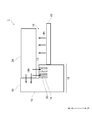
- FIG. 1 is an exploded perspective view of a part of the sensor 1 according to this embodiment.
- the front, rear, left, right, and up and down are based on those shown in FIG.
- the metal lid 20 is configured to cover the opening 15 of the metal housing 10 from above.
- the sensor 1 is described as an example of a photoelectric sensor, but the present invention is not limited to this, and the sensor 1 can be used for various types of sensors.
- the sensor 1 is a photoelectric sensor for detecting the presence of an object by projecting or receiving light.
- the sensor 1 includes, for example, as shown in FIG. 1, a metal housing 10, a metal lid 20, a cover lens 30, and a lens cover 35. Further, the sensor 1 may be provided with a display unit (not shown) for displaying various numerical values.
- the display unit is, for example, an organic EL display, a liquid crystal display, or the like.
- the metal casing 10 is a component for housing an optical component.
- the metal housing 10 is provided with an opening 15 and an edge 11.
- the metal housing 10 is formed of a metal such as stainless steel and may have, for example, a substantially rectangular parallelepiped shape. Inside the metal housing 10, optical components including a sensor element (not shown) and a circuit board (see FIG. 2) electrically connected to the sensor element are housed.
- a substantially rectangular parallelepiped shape may include surfaces other than the six surfaces forming the rectangular parallelepiped, or may not have all the internal angles of 90 degrees, and is a strict rectangular solid shape. It means that they may have different shapes.
- the metal lid 20 is made of a metal such as stainless steel, and is formed so as to cover the opening 15 of the metal housing 10.
- the edge 11 defines an opening 15.
- the edge portion 11 has a first edge portion 12 and a second edge portion 13.
- the first edge portion 12 is formed so as to surround and fix the entire outer circumference of the metal lid 20 when the metal lid 20 is fitted into the first edge portion 12.
- the second edge portion 13 is formed so as to overlap the outer peripheral portion of the metal lid 20 when the metal lid 20 is fitted into the first edge portion 12 and placed on the second edge portion 13. Further, the second edge portion 13 defines the opening portion 15 and includes a joining region between the metal housing 10 and the metal lid 20. By joining the metal casing 10 and the metal lid 20 at the second edge portion 13, the optical components housed in the metal casing 10 are sealed.
- a light emitting / receiving opening 37 for passing light to be projected or received is provided on the front surface of the metal housing 10, and a cover lens 30 covering the light emitting / receiving opening 37 and a cover lens 30 are fixed. Then, the lens cover 35 is fitted.
- Optical parts are parts of an optical system that projects or receives light on an object to be detected.
- the optical component includes a sensor element and a circuit board electrically connected to the sensor element.
- the sensor element is, for example, a light projecting element and/or a light receiving element.
- the light projecting element for example, an element such as an LED (light emitting diode) or an LD (laser diode) may be used.
- the optical component includes a light projecting lens and a light receiving lens. Further, the optical component may include, for example, an amplifier for amplifying the signal received by the light receiving element.
- FIG. 2 is an enlarged schematic cross-sectional view of the bonded portion between the metal housing 10 and the metal lid 20.
- the circuit board 40 is housed in the metal casing 10.
- the circuit board 40 may have a control circuit for the organic EL display, for example, when the organic EL display is used for the display unit.
- the metal lid 20 is sealed by adhesion, so that the sensor 1 is compared with welding or the like by laser welding. The influence of heat on the organic EL display can be reduced.
- the circuit board 40 may have a laser control circuit, for example, when an LD is used for the light projecting element. With such a configuration, in the sensor 1, heat generated from the laser can be transferred to the metal housing 10 via the portion where the metal housing 10 and the metal lid 20 are in contact with each other.
- the second edge 13 of the metal housing 10 is provided with one or more recesses 14.
- the recess 14 is provided in the second edge portion 13, but may be provided in the metal lid 20, or the metal lid 20 and the second edge portion 13, respectively.
- the metal lid 20 is bonded to the second edge portion 13 by the portion of the adhesive 50 filled in the recess 14 located in the area of the opening end of the recess 14.
- the heat emitted from the circuit board 40 and transferred to the metal lid 20 is also transferred to the metal housing 10 via the contact portion between the metal housing 10 and the metal lid 20. It is possible to reduce concentration on the metal lid 20. Thereby, in the sensor 1 in which the metal lid 20 is bonded to the metal housing 10, the heat dissipation can be improved.
- the recess 14 may be, for example, a columnar hole extending in the vertical direction.
- the adhesive 50 filled in the recess 14 can be formed so as to extend in the direction perpendicular to the portion located in the region of the opening end of the recess 14.
- the precision processing is not required to form the recess 14 in the metal housing 10 or the metal lid 20, the cost for metal processing can be reduced.
- the depth of the recess 14 may be selected, for example, so that the adhesive strength of the adhesive 50 is maximized. It is generally known that the adhesive strength of an adhesive changes depending on the thickness of the adhesive layer of the adhesive. For example, if the adhesive layer is too thin, it may be vulnerable to peeling or impact, and on the contrary, if the adhesive layer is too thick, it may be vulnerable to shearing or tension. Therefore, by selecting the depth of the recess 14 so that the adhesive strength of the adhesive 50 is maximized, the adhesive strength between the metal housing 10 and the metal lid 20 can be improved in the sensor 1.
- FIG. 3 is a schematic view of a part of the bonding surface of the metal housing 10 viewed from above.
- the second edge portion 13 of the metal housing 10 is provided with one or more concave portions 14 each having a circular opening end.
- the shape of the opening end is not limited to a circular shape, and may be any shape as long as a certain area can be secured at the opening end.
- the width W of the second edge portion 13 serves as an adhesion margin for adhering the metal housing 10 and the metal lid 20.
- the width W is 0. It may be 5 to 2 mm.
- the adhesive 50 adheres the metal lid 20 to the second edge portion 13 by a portion located in the region of the open end of the recess 14 (the portion described by the dotted line pattern in FIG. 3).
- the portion is an adhesion surface between the second edge portion 13 and the metal lid 20 in the recess 14.
- the total area of the bonding surface may be half or less of the area of the region where the second edge portion 13 and the metal lid 20 overlap.
- the overlapping region is a region overlapping the metal lid 20 in the region of the second edge portion 13 including the adhesive surface of the recess 14.
- the sensor 1 can easily transfer heat from the metal lid 20 to the metal housing 10, and can improve heat dissipation. Further, according to the above configuration, since it is not necessary to control the bonding surface of the concave portion 14 by the size of the bonding region of the metal casing 10 with the metal lid 20, the influence of the accuracy variation of the size on the bonding strength is eliminated. be able to.
- a metal housing (10) that houses a circuit board (40) electrically connected to a sensor element and is provided with an opening (15) and an edge (11) that defines the opening (15).
- a metal lid (20) adhered to the edge (11) so as to cover the opening (15) is provided.
- One or more recesses (14) are provided in at least one of the edge portion (11) and the metal lid (20), and the recess (14) of the adhesive (50) filled in the recess (14). ),
- the metal lid (20) is adhered to the edge (11) by a portion located in the region of the open end. Sensor (1).
Landscapes
- Microelectronics & Electronic Packaging (AREA)
- Engineering & Computer Science (AREA)
- Physics & Mathematics (AREA)
- Thermal Sciences (AREA)
- Sustainable Development (AREA)
- Inorganic Chemistry (AREA)
- Chemical & Material Sciences (AREA)
- Life Sciences & Earth Sciences (AREA)
- Optics & Photonics (AREA)
- General Physics & Mathematics (AREA)
- Switches Operated By Changes In Physical Conditions (AREA)
- Casings For Electric Apparatus (AREA)
- Cooling Or The Like Of Semiconductors Or Solid State Devices (AREA)
- Photo Coupler, Interrupter, Optical-To-Optical Conversion Devices (AREA)
- Switch Cases, Indication, And Locking (AREA)
- Electroluminescent Light Sources (AREA)
Abstract
金属筐体に金属蓋が接着されたセンサにおいて、放熱性を向上することができる。センサ1は、センサ素子と電気的に接続された回路基板40を収容し、開口部15と開口部15を画成する縁部11とが設けられた金属筐体10と、開口部15を覆うよう、縁部11に接着された金属蓋20と、を備え、縁部11及び金属蓋20の少なくともいずれかに凹部14が1つ以上設けられ、当該凹部14内に充填された接着剤50のうち凹部14の開口端の領域に位置する部分によって、縁部11に金属蓋20が接着されている。
Description
本発明は、センサに関する。
センサにおいて、センサ素子や当該センサ素子と電気的に接続された回路基板等を収容する筐体と、当該筐体の開口部を覆うための蓋とを備えるものがある。また、センサにおいて、これら筐体と蓋とが共に金属製の場合、レーザ溶接によって金属筐体を金属蓋で封止する方法がある。例えば下記特許文献1には、本体ケースの側面に設けられた側面開口部を覆うように本体カバーが組付けられており、本体カバーは、本体ケースの側面開口部の周縁と全周にわたってレーザ溶接されることにより本体ケースに固定されているセンサ機器が開示されている。
センサにおいて、各種数値を表示するための表示部として有機ELディスプレイを備えた場合、上記のとおり金属筐体と金属蓋とをレーザ溶接すると、当該有機ディスプレイがレーザ溶接の際の熱で劣化してしまう問題がある。
上記有機ディスプレイの劣化を防止するため、例えば、レーザ溶接に代わって金属筐体と金属蓋とを接着剤で固定する方法がある。しかしながら、このような固定方法では、接着剤の熱伝導率は金属に比べると低いため、図4に例示するように、従来のセンサ60において、金属筐体100に収容された回路基板400から発せられた熱が、接着剤500の層の影響で金属蓋200以外に放熱することが難しくなる。このように、金蔵筐体と金属蓋とを接着剤で固定すると、センサの放熱性が悪くなる問題があった。
そこで、本発明は、金属筐体に金属蓋が接着されたセンサにおいて、放熱性を向上することを目的とする。
本発明の一態様に係るセンサは、センサ素子と電気的に接続された回路基板を収容し、開口部と開口部を画成する縁部とが設けられた金属筐体と、開口部を覆うよう、縁部に接着された金属蓋と、を備え、縁部及び金属蓋の少なくともいずれかに凹部が1つ以上設けられ、当該凹部内に充填された接着剤のうち凹部の開口端の領域に位置する部分によって、縁部に金属蓋が接着されている。
この態様によれば、センサは、回路基板から発せられて金属蓋に伝わった熱が、金属筐体の縁部又は金属蓋の凹部が設けられた部分以外の当該縁部と金属蓋とが接触する部分を介して金属筐体にも伝わる。このため、この態様によれば、センサは、金属蓋に伝わった熱が金属蓋に集中することを低減することができる。これにより、金属筐体10に金属蓋20が接着されているセンサにおいて、放熱性を向上することができる。
上記態様において、凹部は、柱状の穴であってもよい。
この態様によれば、凹部に充填された接着剤において、凹部の開口端の領域に位置する部分に対して垂直方向に延在して形成することができるため、凹部の開口端の部分に代えて、金属筐体の縁部と金属蓋とが接触する部分を確保することができる。
上記態様において、凹部における縁部と金属蓋との接着面の総面積が、縁部と金属蓋の重なる領域の面積の半分以下であってもよい。
この態様によれば、金属筐体の縁部又は金属蓋において、凹部における接着面に代えて、金属筐体の縁部と金属蓋とが接触する部分を確保することができる。これにより、センサは、金属蓋から金属筐体に熱を伝わりやすくすることができ、放熱性を向上することができる。
上記態様において、回路基板は、有機ELディスプレイの制御回路を有してもよい。
この態様によれば、センサにおいて、液晶ディスプレイ等と比較して熱に弱い有機ELディスプレイを備えた場合、接着により金属蓋を封止するため、レーザ溶接による溶着等と比較して、当該有機ELディスプレイへの熱の影響を低減することができる。
上記態様において、回路基板は、レーザの制御回路を有してもよい。
この態様によれば、センサ素子にレーザを備えた場合、当該レーザから発生する熱を、金属筐体の縁部と金属蓋とが接触する部分を介して金属筐体に伝えることができる。
本発明によれば、金属筐体に金属蓋が接着されたセンサにおいて、放熱性を向上することができる。
添付図面を参照して、本発明の好適な実施形態について説明する。なお、各図において、同一の符号を付したものは、同一又は同様の構成を有する。
図4は、従来のセンサ60の金属筐体100と金属蓋200との接着部分を拡大して模式的に示す断面図である。センサ60は、センサ素子(不図示)と、センサ素子と電気的に接続された回路基板400と、金属筐体100と、金属蓋200とを備える。センサ60は、金属筐体100内部にセンサ素子及び回路基板400を収容して、金属筐体100に金属蓋200を取り付けて組み立てられる。
金属蓋200は、金属筐体100の開口部を覆うように金属筐体100に接合される。金属蓋200は、具体的には、金属筐体100の開口部を画成する縁部110に嵌め込まれて、接着剤500の層を挟んで金属筐体100と接合される。そのため、従来のセンサ60は、回路基板400から発せられた熱が、接着剤500の熱伝導率が金属筐体100と比べて低いことにより、金属蓋200と回路基板400とに集中してしまう。
図1を参照して、本実施形態に係るセンサ1の金属筐体10と金属蓋20の全体構成について説明する。図1は、本実施形態に係るセンサ1の一部の分解斜視図である。説明の便宜上、前後左右及び上下に関しては、図1に示すものを基準とする。図1の例では、金属蓋20は、上方から金属筐体10の開口部15を覆う構成となる。本例では、センサ1は光電センサを例に説明するが、これに限る主旨ではなく、センサ1は様々な種類のセンサに用いることができる。
センサ1は、投光又は受光により、物体の存在等を検出するための光電センサである。センサ1は、例えば、図1に示すように、金属筐体10と、金属蓋20と、カバーレンズ30と、レンズカバー35とを備えている。また、センサ1は、各種数値で表示するための表示部(不図示)を設けてもよい。表示部は、例えば、有機ELディスプレイ、又は液晶ディスプレイ等である。
金属筐体10は、光学部品を収容するための部品である。金属筐体10は、開口部15と、縁部11とが設けられている。金属筐体10は、ステンレス等の金属により形成され、例えば、略直方体形状を有していてもよい。金属筐体10の内部には、センサ素子(不図示)と当該センサ素子に電気的に接続された回路基板(図2参照)とを含む光学部品が収容されている。なお、金属筐体10において、「略直方体形状」を有するとは、直方体を構成する六面以外の面を含んだり、内角が全て90度とならなかったりしてもよく、厳密な直方体状と異なる形状であってもよいことを意味する。
金属蓋20は、ステンレス等の金属により形成され、金属筐体10の開口部15を覆うように形成されている。
縁部11は、開口部15を画成する。縁部11は、第1縁部12と第2縁部13とを有する。第1縁部12は、金属蓋20が第1縁部12に嵌め込まれた際に、金属蓋20の外周全体を囲んで固定するように形成されている。
第2縁部13は、金属蓋20が第1縁部12に嵌め込まれて第2縁部13に載置された際に、金属蓋20の外周部分と重なるように形成されている。また、第2縁部13は、開口部15を画成し、金属筐体10と金属蓋20との接合領域を含む。第2縁部13における金属筐体10と金属蓋20との接合により、金属筐体10に収容されている光学部品が封止される。
金属筐体10の前面には、投光又は受光する光を通過させるための投受光用開口部37が設けられており、投受光用開口部37を覆うカバーレンズ30と、カバーレンズ30を固定するとレンズカバー35が嵌め込まれている。
光学部品は、検出対象の物体に対して、投光又は受光する光学系の部品である。光学部品は、センサ素子と、センサ素子に電気的に接続された回路基板とを含む。センサ素子は、例えば、投光素子及び/又は受光素子等である。投光素子は、例えば、LED(発光ダイオード)又はLD(レーザダイオード)等の素子を用いてもよい。また、光学部品は、投光レンズや受光レンズを含む。また、光学部品は、例えば、受光素子により受光された信号を増幅処理するためのアンプを含んでもよい。
図2を参照して、本実施形態に係る金属筐体10と金属蓋20との接着剤50による接着について説明する。図2は、金属筐体10と金属蓋20との接着部分を拡大して模式的に示す断面図である。
図2に示すように、回路基板40は、金属筐体10に収容されている。回路基板40は、例えば、上記表示部に有機ELディスプレイが用いられる場合等において、当該有機ELディスプレイの制御回路を有していてもよい。このような構成により、センサ1において、液晶ディスプレイ等と比較して熱に弱い有機ELディスプレイを備えた場合において、接着により金属蓋20を封止するため、レーザ溶接による溶着等と比較して当該有機ELディスプレイへの熱の影響を低減することができる。
回路基板40は、例えば、投光素子にLDが用いられる場合等において、レーザの制御回路を有していてもよい。このような構成により、センサ1において、レーザから発生する熱を、金属筐体10と金属蓋20とが接触する部分を介して金属筐体10に伝えることができる。
金属筐体10の第2縁部13には、1つ以上の凹部14が設けられている。なお、図2の例では、凹部14は、第2縁部13に設けられているが、金属蓋20又は金属蓋20と第2縁部13のそれぞれに設けられてもよい。凹部14内に充填された接着剤50のうち凹部14の開口端の領域に位置する部分によって、第2縁部13に金属蓋20が接着されている。
上記構成によれば、センサ1は、回路基板40から発せられて金属蓋20に伝わった熱が、金属筐体10と金属蓋20とが接触する部分を介して金属筐体10にも伝わるため、金属蓋20に集中することを低減することができる。これにより、金属筐体10に金属蓋20が接着されているセンサ1において、放熱性を向上することができる。
凹部14は、例えば、上下方向に延在する柱状の穴であってもよい。このような構成によれば、凹部14に充填された接着剤50において、凹部14の開口端の領域に位置する部分に対して垂直方向に延在して形成することができる。これにより、接着剤50の上記凹部14の開口端の領域に位置する部分に代えて、金属筐体10の第2縁部13と金属蓋20とが接触する部分を確保することができる。また、上記構成によれば、金属筐体10又は金属蓋20における凹部14の形成には精密加工が必要ないため、金属加工のためのコストを低減することができる。
凹部14の深さは、例えば、接着剤50による接着強度が最大となるよう選択されてもよい。一般的に、接着剤による接着強度が接着剤の接着層の厚さによって変化することは知られている。例えば、接着層が薄くなり過ぎると剥離や衝撃に弱くなり、反対に接着層が厚くなり過ぎるとせん断や引張に弱くなることがある。このため、凹部14の深さが接着剤50による接着強度が最大となるよう選択することにより、センサ1において、金属筐体10と金属蓋20との接着強度を向上することができる。
図3を参照して、金属筐体10における金属筐体10と金属蓋20との接着面について説明する。図3は、金属筐体10の当該接着面の一部を上方から視た模式図である。図3に示すように、金属筐体10の第2縁部13において、開口端が円形の凹部14が1つ以上設けられている。なお、当該開口端の形状は、円形に限定されず、開口端における一定の面積が確保できれば、どのような形状でもよい。また、第2縁部13の幅Wは、金属筐体10と金属蓋20とを接着する接着代となる。例えば、金属筐体10が、上方から視て、奥行きが約15mm、短軸方向の長さが約30mm、長軸方向の長さ約40mm程度の略直方体形状の場合、幅Wは、0.5~2mmであってもよい。
接着剤50は、凹部14の開口端の領域に位置する部分(図3において点線パターンで記載している部分)によって、第2縁部13に金属蓋20を接着している。当該部分は、凹部14における第2縁部13と金属蓋20との接着面である。当該接着面の総面積は、第2縁部13と金属蓋20とが重なる領域の面積の半分以下であってもよい。当該重なる領域は、図3の例では、凹部14の接着面を含む第2縁部13の領域において、金属蓋20と重なる領域である。
上記構成によれば、凹部14における上記接着面の総面積に代えて、金属筐体10と金属蓋20とが接触する部分の面積を確保することができる。これにより、センサ1は、金属蓋20から金属筐体10に熱を伝わりやすくすることができ、放熱性を向上することができる。また、上記構成によれば、凹部14における上記接着面を金属筐体10における金属蓋20との接合領域の寸法で制御する必要がないため、当該寸法の精度ばらつきによる接合強度への影響をなくすことができる。
以上説明した実施形態は、本発明の理解を容易にするためのものであり、本発明を限定して解釈するためのものではない。実施形態が備える各要素並びにその配置、材料、条件、形状及びサイズ等は、例示したものに限定されるわけではなく適宜変更することができる。また、異なる実施形態で示した構成同士を部分的に置換し又は組み合わせることが可能である。
[附記]
センサ素子と電気的に接続された回路基板(40)を収容し、開口部(15)と前記開口部(15)を画成する縁部(11)とが設けられた金属筐体(10)と、
前記開口部(15)を覆うよう、前記縁部(11)に接着された金属蓋(20)と、を備え、
前記縁部(11)及び前記金属蓋(20)の少なくともいずれかに凹部(14)が1つ以上設けられ、当該凹部(14)内に充填された接着剤(50)のうち前記凹部(14)の開口端の領域に位置する部分によって、前記縁部(11)に前記金属蓋(20)が接着されている、
センサ(1)。
センサ素子と電気的に接続された回路基板(40)を収容し、開口部(15)と前記開口部(15)を画成する縁部(11)とが設けられた金属筐体(10)と、
前記開口部(15)を覆うよう、前記縁部(11)に接着された金属蓋(20)と、を備え、
前記縁部(11)及び前記金属蓋(20)の少なくともいずれかに凹部(14)が1つ以上設けられ、当該凹部(14)内に充填された接着剤(50)のうち前記凹部(14)の開口端の領域に位置する部分によって、前記縁部(11)に前記金属蓋(20)が接着されている、
センサ(1)。
1、60…センサ、10、100…金属筐体、11、110…縁部、12、120…第1縁部、13、130…第2縁部、14…凹部、15…開口部、20、200…金属蓋、30…カバーレンズ、35…レンズカバー、37…投受光用開口部、40、400…回路基板、50、500…接着剤、W…幅
Claims (5)
- センサ素子と電気的に接続された回路基板を収容し、開口部と前記開口部を画成する縁部とが設けられた金属筐体と、
前記開口部を覆うよう、前記縁部に接着された金属蓋と、を備え、
前記縁部及び前記金属蓋の少なくともいずれかに凹部が1つ以上設けられ、当該凹部内に充填された接着剤のうち前記凹部の開口端の領域に位置する部分によって、前記縁部に前記金属蓋が接着されている、
センサ。 - 前記凹部は、柱状の穴である、
請求項1に記載のセンサ。 - 前記凹部における前記縁部と前記金属蓋との接着面の総面積が、前記縁部と前記金属蓋の重なる領域の面積の半分以下である、
請求項1または2に記載のセンサ。 - 前記回路基板は、有機ELディスプレイの制御回路を有する、
請求項1から3のいずれか一項に記載のセンサ。 - 前記回路基板は、レーザの制御回路を有する、
請求項1から4のいずれか一項に記載のセンサ。
Priority Applications (4)
| Application Number | Priority Date | Filing Date | Title |
|---|---|---|---|
| KR1020217025102A KR102683401B1 (ko) | 2019-03-04 | 2020-02-26 | 센서 |
| CN202080013325.7A CN113424285A (zh) | 2019-03-04 | 2020-02-26 | 传感器 |
| EP20766614.0A EP3937201A4 (en) | 2019-03-04 | 2020-02-26 | SENSOR |
| US17/432,940 US11832499B2 (en) | 2019-03-04 | 2020-02-26 | Sensor |
Applications Claiming Priority (2)
| Application Number | Priority Date | Filing Date | Title |
|---|---|---|---|
| JP2019-038686 | 2019-03-04 | ||
| JP2019038686A JP7116923B2 (ja) | 2019-03-04 | 2019-03-04 | センサ |
Publications (1)
| Publication Number | Publication Date |
|---|---|
| WO2020179573A1 true WO2020179573A1 (ja) | 2020-09-10 |
Family
ID=72338659
Family Applications (1)
| Application Number | Title | Priority Date | Filing Date |
|---|---|---|---|
| PCT/JP2020/007689 Ceased WO2020179573A1 (ja) | 2019-03-04 | 2020-02-26 | センサ |
Country Status (6)
| Country | Link |
|---|---|
| US (1) | US11832499B2 (ja) |
| EP (1) | EP3937201A4 (ja) |
| JP (1) | JP7116923B2 (ja) |
| KR (1) | KR102683401B1 (ja) |
| CN (1) | CN113424285A (ja) |
| WO (1) | WO2020179573A1 (ja) |
Families Citing this family (1)
| Publication number | Priority date | Publication date | Assignee | Title |
|---|---|---|---|---|
| KR102873924B1 (ko) * | 2023-10-16 | 2025-10-29 | (주)파트론 | 타이어 모니터링 장치 |
Citations (4)
| Publication number | Priority date | Publication date | Assignee | Title |
|---|---|---|---|---|
| JP2006524910A (ja) * | 2003-03-21 | 2006-11-02 | タイコ エレクトロニクス プレテマ ゲゼルシャフト ミット ベシュレンクテル ハフツンク ウント コンパニー ケーゲー | 構造ユニット、及び構造ユニットの製造方法 |
| JP2010272561A (ja) * | 2009-05-19 | 2010-12-02 | Hitachi Kokusai Electric Inc | 防水構造 |
| JP2017157487A (ja) * | 2016-03-03 | 2017-09-07 | オムロン株式会社 | センサ機器 |
| JP2018152227A (ja) * | 2017-03-13 | 2018-09-27 | オムロン株式会社 | センサ機器 |
Family Cites Families (14)
| Publication number | Priority date | Publication date | Assignee | Title |
|---|---|---|---|---|
| DE2845400B2 (de) | 1978-10-18 | 1981-04-30 | GAO Gesellschaft für Automation und Organisation mbH, 8000 München | Ausweiskarte mit reliefartiger Oberfläche |
| JPS5597989U (ja) * | 1978-12-28 | 1980-07-08 | ||
| JPS6394626U (ja) | 1986-12-12 | 1988-06-18 | ||
| JPH04159799A (ja) * | 1990-10-23 | 1992-06-02 | Nec Corp | 混成集積回路 |
| US7123440B2 (en) * | 2003-09-29 | 2006-10-17 | Hitachi Global Storage Technologies Netherlands B.V. | Hermetically sealed electronics arrangement and approach |
| JP2007035536A (ja) * | 2005-07-29 | 2007-02-08 | Rohm Co Ltd | フラットパネルディスプレイ |
| JP4929659B2 (ja) * | 2005-09-26 | 2012-05-09 | 株式会社ジェイテクト | 電子制御装置 |
| JP4924143B2 (ja) * | 2007-03-28 | 2012-04-25 | マツダ株式会社 | 金属製ワークの接合方法 |
| JP2009246032A (ja) * | 2008-03-28 | 2009-10-22 | Panasonic Corp | 半導体装置 |
| US8305763B2 (en) * | 2008-10-27 | 2012-11-06 | Keihin Corporation | Housing case for electronic circuit board |
| JP5005654B2 (ja) * | 2008-10-27 | 2012-08-22 | 株式会社ケーヒン | 電子回路基板の収容ケース |
| JP5350311B2 (ja) * | 2010-04-01 | 2013-11-27 | 日立オートモティブシステムズ株式会社 | 車載用電子機器 |
| KR20160076857A (ko) * | 2014-12-23 | 2016-07-01 | 엘지전자 주식회사 | 이동 단말기 및 그의 컨텐츠 제어방법 |
| JP6939344B2 (ja) * | 2017-09-28 | 2021-09-22 | セイコーエプソン株式会社 | 原子発振器およびシステム |
-
2019
- 2019-03-04 JP JP2019038686A patent/JP7116923B2/ja active Active
-
2020
- 2020-02-26 CN CN202080013325.7A patent/CN113424285A/zh active Pending
- 2020-02-26 WO PCT/JP2020/007689 patent/WO2020179573A1/ja not_active Ceased
- 2020-02-26 KR KR1020217025102A patent/KR102683401B1/ko active Active
- 2020-02-26 EP EP20766614.0A patent/EP3937201A4/en active Pending
- 2020-02-26 US US17/432,940 patent/US11832499B2/en active Active
Patent Citations (5)
| Publication number | Priority date | Publication date | Assignee | Title |
|---|---|---|---|---|
| JP2006524910A (ja) * | 2003-03-21 | 2006-11-02 | タイコ エレクトロニクス プレテマ ゲゼルシャフト ミット ベシュレンクテル ハフツンク ウント コンパニー ケーゲー | 構造ユニット、及び構造ユニットの製造方法 |
| JP2010272561A (ja) * | 2009-05-19 | 2010-12-02 | Hitachi Kokusai Electric Inc | 防水構造 |
| JP2017157487A (ja) * | 2016-03-03 | 2017-09-07 | オムロン株式会社 | センサ機器 |
| JP6394626B2 (ja) | 2016-03-03 | 2018-09-26 | オムロン株式会社 | センサ機器 |
| JP2018152227A (ja) * | 2017-03-13 | 2018-09-27 | オムロン株式会社 | センサ機器 |
Non-Patent Citations (1)
| Title |
|---|
| See also references of EP3937201A4 |
Also Published As
| Publication number | Publication date |
|---|---|
| US11832499B2 (en) | 2023-11-28 |
| EP3937201A1 (en) | 2022-01-12 |
| KR102683401B1 (ko) | 2024-07-08 |
| KR20210111835A (ko) | 2021-09-13 |
| JP2020144992A (ja) | 2020-09-10 |
| EP3937201A4 (en) | 2022-11-30 |
| JP7116923B2 (ja) | 2022-08-12 |
| CN113424285A (zh) | 2021-09-21 |
| US20220173175A1 (en) | 2022-06-02 |
Similar Documents
| Publication | Publication Date | Title |
|---|---|---|
| JP6447542B2 (ja) | センサ機器およびその製造方法 | |
| JP6991463B2 (ja) | 光電センサ及びその製造方法 | |
| WO2019196525A1 (zh) | 激光投射结构和电子装置 | |
| JP7757522B2 (ja) | カメラまたはセンサのためのイメージャモジュール | |
| WO2020179573A1 (ja) | センサ | |
| WO2003019263A1 (en) | Optical isolator module | |
| JP2001250979A (ja) | 光センサ | |
| JP4043204B2 (ja) | 火災検知器 | |
| JP2004200944A (ja) | 携帯端末機器及びそれに用いるカメラユニット固定構造 | |
| CN108490572B (zh) | 激光投射模组、深度相机及电子装置 | |
| JP6991462B2 (ja) | 小型光電センサ | |
| JP6872174B2 (ja) | 光電センサ | |
| JP5193492B2 (ja) | 光半導体デバイス | |
| JP4121033B2 (ja) | 熱感知器 | |
| JP6995288B2 (ja) | 光電センサ | |
| JP3736536B2 (ja) | 光電センサ | |
| CN111712978B (zh) | 盖部以及半导体激光模块 | |
| JP7062362B2 (ja) | 放射線検出器および放射線検出装置 | |
| WO2002037138A1 (en) | Radiation detector | |
| CN212517882U (zh) | 一种激光器 | |
| JP2018204966A (ja) | ガス濃度モニタ用プローブ及びガス濃度モニタ | |
| CN114137597A (zh) | 放射线检测器和开孔装置 | |
| JPH02260658A (ja) | 固体撮像部品 | |
| JP2020101883A (ja) | 携帯型入力端末 | |
| WO2019026387A1 (ja) | 生体情報測定装置 |
Legal Events
| Date | Code | Title | Description |
|---|---|---|---|
| 121 | Ep: the epo has been informed by wipo that ep was designated in this application |
Ref document number: 20766614 Country of ref document: EP Kind code of ref document: A1 |
|
| ENP | Entry into the national phase |
Ref document number: 20217025102 Country of ref document: KR Kind code of ref document: A |
|
| NENP | Non-entry into the national phase |
Ref country code: DE |
|
| ENP | Entry into the national phase |
Ref document number: 2020766614 Country of ref document: EP Effective date: 20211004 |