WO2020183552A1 - Dispositif de dépôt et procédé de fabrication de dispositif d'affichage - Google Patents
Dispositif de dépôt et procédé de fabrication de dispositif d'affichage Download PDFInfo
- Publication number
- WO2020183552A1 WO2020183552A1 PCT/JP2019/009531 JP2019009531W WO2020183552A1 WO 2020183552 A1 WO2020183552 A1 WO 2020183552A1 JP 2019009531 W JP2019009531 W JP 2019009531W WO 2020183552 A1 WO2020183552 A1 WO 2020183552A1
- Authority
- WO
- WIPO (PCT)
- Prior art keywords
- substrate
- vapor deposition
- mask
- alignment
- touch plate
- Prior art date
- Legal status (The legal status is an assumption and is not a legal conclusion. Google has not performed a legal analysis and makes no representation as to the accuracy of the status listed.)
- Ceased
Links
Images










Classifications
-
- C—CHEMISTRY; METALLURGY
- C23—COATING METALLIC MATERIAL; COATING MATERIAL WITH METALLIC MATERIAL; CHEMICAL SURFACE TREATMENT; DIFFUSION TREATMENT OF METALLIC MATERIAL; COATING BY VACUUM EVAPORATION, BY SPUTTERING, BY ION IMPLANTATION OR BY CHEMICAL VAPOUR DEPOSITION, IN GENERAL; INHIBITING CORROSION OF METALLIC MATERIAL OR INCRUSTATION IN GENERAL
- C23C—COATING METALLIC MATERIAL; COATING MATERIAL WITH METALLIC MATERIAL; SURFACE TREATMENT OF METALLIC MATERIAL BY DIFFUSION INTO THE SURFACE, BY CHEMICAL CONVERSION OR SUBSTITUTION; COATING BY VACUUM EVAPORATION, BY SPUTTERING, BY ION IMPLANTATION OR BY CHEMICAL VAPOUR DEPOSITION, IN GENERAL
- C23C14/00—Coating by vacuum evaporation, by sputtering or by ion implantation of the coating forming material
- C23C14/22—Coating by vacuum evaporation, by sputtering or by ion implantation of the coating forming material characterised by the process of coating
- C23C14/24—Vacuum evaporation
-
- C—CHEMISTRY; METALLURGY
- C23—COATING METALLIC MATERIAL; COATING MATERIAL WITH METALLIC MATERIAL; CHEMICAL SURFACE TREATMENT; DIFFUSION TREATMENT OF METALLIC MATERIAL; COATING BY VACUUM EVAPORATION, BY SPUTTERING, BY ION IMPLANTATION OR BY CHEMICAL VAPOUR DEPOSITION, IN GENERAL; INHIBITING CORROSION OF METALLIC MATERIAL OR INCRUSTATION IN GENERAL
- C23C—COATING METALLIC MATERIAL; COATING MATERIAL WITH METALLIC MATERIAL; SURFACE TREATMENT OF METALLIC MATERIAL BY DIFFUSION INTO THE SURFACE, BY CHEMICAL CONVERSION OR SUBSTITUTION; COATING BY VACUUM EVAPORATION, BY SPUTTERING, BY ION IMPLANTATION OR BY CHEMICAL VAPOUR DEPOSITION, IN GENERAL
- C23C14/00—Coating by vacuum evaporation, by sputtering or by ion implantation of the coating forming material
- C23C14/22—Coating by vacuum evaporation, by sputtering or by ion implantation of the coating forming material characterised by the process of coating
- C23C14/50—Substrate holders
Definitions
- the present invention relates to a method for manufacturing a vapor deposition apparatus and a display apparatus.
- Patent Documents 1 and 2 disclose a vapor deposition apparatus in which a substrate is arranged between a vapor deposition mask and a magnet, and the vapor deposition mask adheres to the substrate by the magnetic force of the magnet.
- the substrate alignment marks provided on both ends of the substrate, which are the objects to be deposited, and the mask alignment provided on the thin-film deposition mask are known that the alignment position confirmation for confirming whether or not the mark is within a predetermined allowable range is performed before the vapor deposition process is performed.
- the alignment position can not be confirmed efficiently, and there is a problem that the vapor deposition process and the manufacturing time of the display device cannot be shortened. ..
- the central portion of the substrate is first placed on the vapor deposition mask in a state of being bent by the weight of the substrate. After that, in the conventional thin-film deposition apparatus, the substrate is gradually placed on the vapor deposition mask in the direction from the center to both ends of the substrate, and after the entire surface of the substrate comes into contact with the vapor deposition mask, the alignment position is confirmed. It was done. For this reason, in the conventional thin-film deposition apparatus, when the alignment position is confirmed, the substrate alignment marks provided at both ends may be significantly deviated from the mask alignment marks due to the bending of the central portion.
- the present invention has been made in view of the above problems, and an object of the present invention is to realize a vapor deposition device and a method for manufacturing a display device, which can shorten the manufacturing time of the display device.
- the thin-film deposition apparatus is arranged between a thin-film deposition source, a thin-film deposition mask having a mask sheet and a mask frame, a magnet for bringing the mask sheet into close contact with the substrate, and the substrate and the magnet.
- a vapor deposition apparatus including a touch plate to be provided, an elevating device for raising and lowering the substrate with respect to the vapor deposition mask, and an alignment device for aligning the vapor deposition mask with the substrate.
- a plurality of support members that are provided around the substrate and that come into contact with a non-deposited region other than the surface to be vapor-deposited of the substrate to support the substrate, and the plurality of support members that are connected to the plurality of support members.
- the support members are provided with a drive mechanism that drives the support members in the elevating direction of the substrate independently of each other, and the drive mechanism is such that only one end of the substrate is pressed by the touch plate. While driving the support member so as to abut against the vapor deposition mask and pressing the substrate with the touch plate, the other end gradually moves toward the other end of the substrate and the other end becomes the vapor deposition mask. It is a configuration that drives the support member so as to abut.
- the method for manufacturing a display device is a method for manufacturing a display device having a substrate, which comprises a vapor deposition step of performing a vapor deposition process on the substrate by using a vapor deposition mask.
- a second driving step of driving the support member so that the other end of the substrate abuts on the vapor deposition mask gradually toward the other end of the substrate while pressing the substrate is included. , The method.
- FIG. 5 is a cross-sectional view taken along the longitudinal direction of the substrate which schematically shows a part of the vapor deposition process shown in FIG. FIG.
- FIG. 5 is another cross-sectional view along the longitudinal direction of the substrate, schematically showing a part of the vapor deposition process shown in FIG.
- FIG. 5 is another cross-sectional view along the longitudinal direction of the substrate, schematically showing a part of the vapor deposition process shown in FIG.
- FIG. 5 is another cross-sectional view along the longitudinal direction of the substrate, schematically showing a part of the vapor deposition process shown in FIG.
- FIG. 5 is another cross-sectional view along the longitudinal direction of the substrate, schematically showing a part of the vapor deposition process shown in FIG.
- FIG. 5 is another cross-sectional view along the longitudinal direction of the substrate, schematically showing a part of the vapor deposition process shown in FIG.
- FIG. 1 It is sectional drawing along the longitudinal direction of a substrate which shows an example of the schematic structure of the vapor deposition apparatus which concerns on one Embodiment of this invention. It is a perspective view which shows the schematic structure of the vapor deposition apparatus shown in FIG. It is a block diagram which shows an example of the schematic structure of the alignment apparatus included in the vapor deposition apparatus shown in FIG. It is sectional drawing and the plan view which show schematicly superimposing the alignment mark and the through hole for imaging shown in FIG. It is a flow chart which shows typically an example of the vapor deposition process in the vapor deposition apparatus shown in FIG. It is sectional drawing and the side view along the longitudinal direction of a substrate which show schematic part of the vapor deposition process in the vapor deposition apparatus shown in FIG.
- FIG. 5 is a flow chart schematically showing another example of the vapor deposition process in the vapor deposition apparatus shown in FIG. 12.
- FIG. 6 is a cross-sectional view taken along the longitudinal direction of the substrate, schematically showing a part of the vapor deposition process in the thin-film deposition apparatus shown in FIG. 24. It is sectional drawing along the longitudinal direction of a substrate which shows an example of the schematic structure of the vapor deposition apparatus which concerns on another Embodiment of this invention.
- FIG. 6 is a cross-sectional view taken along the longitudinal direction of the substrate, schematically showing a part of the vapor deposition process in the thin-film deposition apparatus shown in FIG. 24. It is sectional drawing along the longitudinal direction of a substrate which shows an example of the schematic structure of the vapor deposition apparatus which concerns on another Embodiment of this invention.
- FIG. 6 is a cross-sectional view taken along the longitudinal direction of the substrate, schematically showing a part of the thin-film deposition process in the thin-film deposition apparatus shown in FIG. It is sectional drawing along the longitudinal direction of a substrate which shows an example of the schematic structure of the vapor deposition apparatus which concerns on another Embodiment of this invention.
- FIG. 8 is a cross-sectional view taken along the longitudinal direction of the substrate which schematically shows a part of the vapor deposition process in the vapor deposition apparatus shown in FIG. 28.
- “same layer” means that they are formed in the same process (film forming step), and “lower layer” means that they are formed in a process prior to the layer to be compared. And “upper layer” means that it is formed in a process after the layer to be compared.
- FIG. 1 is a flowchart showing an example of a manufacturing method of a display device.
- FIG. 2 is a cross-sectional view showing the configuration of a display area of the display device 2.
- a resin layer 12 is formed on a translucent support substrate (for example, mother glass) as shown in FIGS. 1 and 2 (step S1).
- the barrier layer 3 is formed (step S2).
- the TFT layer 4 is formed (step S3).
- the top emission type light emitting element layer 5 is formed (step S4).
- the sealing layer 6 is formed (step S5).
- the top film is attached on the sealing layer 6 (step S6).
- step S7 the support substrate is peeled from the resin layer 12 by irradiation with laser light or the like.
- the lower surface film 10 is attached to the lower surface of the resin layer 12 (step S8).
- step S9 the laminate including the bottom film 10, the resin layer 12, the barrier layer 3, the TFT layer 4, the light emitting element layer 5, and the sealing layer 6 is divided to obtain a plurality of pieces (step S9).
- step S10 the electronic circuit board (for example, the IC chip and the FPC) is mounted on a part (terminal portion) outside the display region (non-display region, frame region) on which the plurality of sub-pixels are formed (step S11).
- steps S1 to S11 are performed by a display device manufacturing apparatus (including a film forming apparatus that performs each step of steps S1 to S5).
- Examples of the material of the resin layer 12 include polyimide and the like.
- the portion of the resin layer 12 can also be replaced with a two-layer resin film (for example, a polyimide film) and an inorganic insulating film sandwiched between them.
- the barrier layer 3 is a layer that prevents foreign matters such as water and oxygen from entering the TFT layer 4 and the light emitting element layer 5, and is formed by, for example, a CVD method, which is a silicon oxide film, a silicon nitride film, or an oxynitride film. It can be composed of a silicon film or a laminated film thereof.
- the TFT layer 4 includes a semiconductor film 15, an inorganic insulating film 16 (gate insulating film) above the semiconductor film 15, a gate electrode GE and a gate wiring GH above the inorganic insulating film 16, a gate electrode GE, and the same.
- a flattening film 21 (interlayer insulating film) above the source wiring SH.
- the semiconductor film 15 is composed of, for example, low-temperature polysilicon (LTPS) or an oxide semiconductor (for example, an In—Ga—Zn—O-based semiconductor), and the transistor (TFT) is configured to include the semiconductor film 15 and the gate electrode GE. Will be done. Although the transistor is shown in the top gate structure in FIG. 2, it may have a bottom gate structure.
- LTPS low-temperature polysilicon
- oxide semiconductor for example, an In—Ga—Zn—O-based semiconductor
- the gate electrode GE, gate wiring GH, capacitive electrode CE, and source wiring SH are composed of, for example, a single layer film or a laminated film of a metal containing at least one of aluminum, tungsten, molybdenum, tantalum, chromium, titanium, and copper. Will be done.
- the TFT layer 4 of FIG. 2 includes one semiconductor layer and three metal layers.
- the inorganic insulating films 16, 18, and 20 can be formed of, for example, a silicon oxide (SiOx) film, a silicon nitride (SiNx) film, or a laminated film thereof formed by a CVD method.
- the flattening film 21 can be made of a coatable organic material such as polyimide or acrylic.
- the light emitting element layer 5 includes an anode 22 (anode) above the flattening film 21, an insulating edge cover 23 covering the edge of the anode 22, and an EL (electroluminescence) active layer above the edge cover 23. 24 and a cathode 25 (cathode) above the active layer 24.
- the edge cover 23 is formed by applying an organic material such as polyimide or acrylic and then patterning by photolithography.
- a subpixel circuit that includes an island-shaped anode 22, an active layer 24, and a cathode 25 for each subpixel, and a light emitting element ES (electroluminescent element) that is a QLED is formed in the light emitting element layer 5 to control the light emitting element ES. Is formed in the TFT layer 4.
- the active layer 24 is composed of, for example, laminating a hole injection layer, a hole transport layer, a light emitting layer, an electron transport layer, and an electron injection layer in order from the lower layer side.
- the light emitting layer is formed in an island shape at the opening (for each sub-pixel) of the edge cover 23 by a vapor deposition method or an inkjet method.
- the other layers are formed in an island shape or a solid shape (common layer). It is also possible to adopt a configuration in which one or more layers out of the hole injection layer, the hole transport layer, the electron transport layer, and the electron injection layer are not formed.
- an island-shaped light emitting layer (corresponding to one sub-pixel) can be formed by applying a solvent in which quantum dots are dispersed by inkjet coating.
- the anode 22 is a reflective electrode having light reflectivity, for example, composed of a laminate of ITO (Indium Tin Oxide) and an alloy containing Ag (silver) or Ag, or a material containing Ag or Al. is there.
- the cathode 25 is a transparent electrode made of a thin film of Ag, Au, Pt, Ni, Ir, a thin film of MgAg alloy, and a translucent conductive material such as ITO and IZO (Indium zinc Oxide).
- the display device is not a top emission type but a bottom emission type, the bottom film 10 and the resin layer 12 are translucent, the anode 22 is a transparent electrode, and the cathode 25 is a reflective electrode.
- the sealing layer 6 is translucent, and has an inorganic sealing film 26 covering the cathode 25, an organic buffer film 27 above the inorganic sealing film 26, and an inorganic sealing film 28 above the organic buffer film 27. And include.
- the sealing layer 6 covering the light emitting element layer 5 prevents foreign matter such as water and oxygen from penetrating into the light emitting element layer 5.
- the inorganic sealing film 26 and the inorganic sealing film 28 are each an inorganic insulating film, and are composed of, for example, a silicon oxide film, a silicon nitride film, a silicon nitride film, or a laminated film thereof formed by a CVD method. be able to.
- the organic buffer film 27 is a translucent organic film having a flattening effect, and can be made of a coatable organic material such as acrylic.
- the organic buffer film 27 can be formed by, for example, inkjet coating, but a bank for stopping the droplets may be provided in the non-display area.
- the bottom film 10 is, for example, a PET film for realizing a display device having excellent flexibility by sticking it to the bottom surface of the resin layer 12 after peeling off the support substrate.
- the functional film 39 has, for example, at least one of an optical compensation function, a touch sensor function, and a protective function.
- a translucent sealing member may be bonded with a sealing adhesive in a nitrogen atmosphere. ..
- the translucent sealing member can be formed of glass, brass, or the like, and is preferably concave.
- One embodiment of the present invention particularly relates to the vapor deposition process in step S4 of the above-mentioned manufacturing method of the display device (display device). Moreover, one embodiment of the present invention relates to a vapor deposition apparatus used for a vapor deposition process in particular.
- FIG. 3 is a cross-sectional view of the substrate 1120 along the longitudinal direction showing a schematic configuration of the vapor deposition apparatus 1100 of the comparative example.
- the vapor deposition apparatus 1100 includes a transport mechanism, a vacuum chamber, a control mechanism, and the like for transporting the substrate 1120. Further, the illustration will be omitted in the subsequent drawings as well.
- the vapor deposition apparatus 1100 of the comparative example includes a vapor deposition source 1160, a mask holder 1113 for holding the vapor deposition mask 1110, an elevating device 1130 for holding the substrate 1120 in an elevating manner, a magnet 1140, and a touch plate.
- the vapor deposition mask 1110 includes a mask sheet 1111 and a mask frame 1112.
- FIG. 4 is an enlarged side view showing a schematic shape of the substrate side surface 1104 of the touch plate 1101 included in the vapor deposition apparatus 1100 of the comparative example shown in FIG.
- the substrate-side surface 1104 of the touch plate 1101 of the comparative example is a smooth surface without any depression or protrusion on the flat surface 1150. Therefore, the touch plate 1101 can abut (surface contact) with the substrate 1120 on the entire surface 1104 on the substrate side.
- the touch plate 1101 is formed of, for example, titanium alloy or stainless steel.
- the substrate 1120 is, for example, a glass substrate. Therefore, the flexibility of the substrate 1120 is higher than the flexibility of the touch plate 1101.
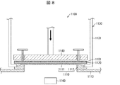
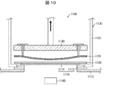
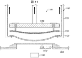
- FIG. 5 is a flow chart schematically showing a vapor deposition process in the vapor deposition apparatus 1100 of the comparative example shown in FIG. 6 to 11 are cross-sectional views taken along the longitudinal direction of the substrate, schematically showing each part of the vapor deposition process shown in FIG.
- step S31 when the substrate 1120 is carried into the vapor deposition apparatus 1100 (step S31), it is sandwiched between the hook 1131 of the elevating apparatus 1130 and the touch plate 1101. Then, in the sandwiched state, the substrate 1120 is carried directly above the vapor deposition mask 1110 so as to be separated from the vapor deposition mask 1110.
- the substrate 1120 is brought close to the vapor deposition mask 1110, and the substrate 1120 is aligned with the vapor deposition mask 1110 (step S32).
- the alignment device that performs alignment first images the alignment marks of the vapor deposition mask 1110 and the substrate 1120 with a camera, and the amount of deviation of the alignment marks of the substrate 1120 with respect to the alignment marks of the vapor deposition mask 1110 from the imaging data. Is measured (step S33). Then, the discrimination unit determines whether the deviation amount is within the threshold range (first allowable range) (step S34).
- step S35 the control unit of the alignment device controls the deviation amount to be 0 and horizontally moves the substrate 1120 to the alignment drive mechanism (step S35). Subsequently, the alignment device repeats steps S33 and S34. If the deviation amount is within the threshold range (Yes) in step S34, the alignment device ends the alignment (step S32).
- the touch plate 1101 presses the substrate 1120 toward the mask sheet 1111 by its own weight. Therefore, the touch plate 1101 and the substrate 1120 are bent downwardly in the direction of gravity together due to their own weight.
- the amount of deviation of the alignment mark of the substrate 1120 with respect to the alignment mark of the vapor deposition mask 1110 is measured in a state where the substrate 1120 is separated from the mask sheet 1111 of the vapor deposition mask 1110. ii) It means that it is determined whether the deviation amount is within the threshold range, and (iii) the deviation amount 0 is controlled as a target to move the substrate 1120 in the horizontal direction. Further, since the substrate 1120 is lowered onto the vapor deposition mask 1110 in a state where the substrate 1120 is in contact with the touch plate 1101 (step S36), the alignment (step S32) is also in a state where the substrate 1120 is in contact with the touch plate 1101. It is done in.
- the substrate 1120 is lowered onto the vapor deposition mask 1110 in a bent state together with the touch plate 1101 (step S36). During this time, the touch plate 1101 continues to press the substrate 1120 toward the vapor deposition mask 1110 by its own weight.
- the magnet 1140 is brought closer to the touch plate 1101 (step S37).
- the magnetic force of the magnet 1140 acting on the mask sheet 1111 increases, so that the mask sheet 1111 is pulled up.
- the touch plate 1101 continues to press the substrate 1120 toward the vapor deposition mask 1110 by its own weight.
- the mask sheet 1111 comes into close contact with the substrate 1120.
- the alignment position confirmation for confirming the position of the alignment mark is performed (step S38).
- the alignment device for confirming the alignment position captures an alignment mark with a camera, measures the amount of deviation (step S39), and determines whether the amount of deviation is within the threshold range (second allowable range) (step S40).
- the substrate 1120, the touch plate 1101 and the magnet 1140 are pulled up to separate the substrate 1120 from the vapor deposition mask 1110 (step S41), return to the alignment (step S32), and step. S35, S33, and S34 are performed again.
- alignment position confirmation means (i) alignment of the substrate 1120 with respect to the alignment mark of the vapor deposition mask 1110 in a state where the hook 1131 of the elevating device 1130 is lowered and the substrate 1120 is in contact with the vapor deposition mask 1110. It means that the amount of deviation of the mark is measured, and (ii) it is determined whether the amount of deviation is within the threshold range.
- the threshold range for alignment position confirmation is wider than the threshold range for alignment.
- step S40 the mask sheet 1111 of the vapor deposition mask 1110 is pulled up by the magnetic force of the magnet 1140, and the substrate 1120 is pressed by the weight of the touch plate 1101. Therefore, the mask sheet 1111 is in close contact with the substrate 1120. Then, when it is within the threshold range (Yes) in step S40, the film is formed by depositing the vapor deposition material on the substrate 1120 in such a close contact state (step S42).
- the magnet 1140 is lifted to separate the magnet 1140 from the touch plate 1101 (step S43). As a result, the magnetic force from the magnet 1140 acting on the vapor deposition mask 1110 is weakened, so that the mask sheet 1111 does not adhere to the substrate 1120.
- step S44 the touch plate 1101 is lifted and the touch plate 1101 is separated from the substrate 1120.
- the touch plate 1101 does not press the substrate 1120.
- step S45 the substrate 1120 is lifted (step S45), and the substrate 1120 is carried out (step S46).
- step S36 when the substrate 1120 is brought into contact with the vapor deposition mask 1110 in step S36, first, the central portion of the substrate 1120 is placed on the vapor deposition mask 1110 in a state of being bent by the weight of the substrate 1120. It had been. Then, the substrate 1120 is gradually placed on the vapor deposition mask 1110 in the direction from the central portion to both ends of the substrate 1120, the entire surface of the substrate 1120 is in contact with the vapor deposition mask 1110, and then the alignment position in step S38. Confirmation was being made.
- the substrate alignment marks provided at both ends may be significantly deviated from the mask alignment marks due to the bending of the central portion.
- these substrate alignment marks and mask alignment marks deviated from the permissible range There were cases where these substrate alignment marks and mask alignment marks deviated from the permissible range.
- FIG. 12 is a cross-sectional view of the substrate 120 along the longitudinal direction showing an example of a schematic configuration of the vapor deposition apparatus 100 according to the first embodiment of the present invention.
- the vapor deposition apparatus 100 includes a transport mechanism, a vacuum chamber, a control mechanism, and the like for transporting the substrate 120.
- FIG. 13 is a perspective view showing a schematic configuration of the vapor deposition apparatus 100 shown in FIG.
- the magnet 140, the touch plate 101, the substrate 120, the vapor deposition mask 110, and the hook 131 are shown, and the other configurations are not shown.
- the thin-film deposition apparatus 100 uses a thin-film deposition source 160 for vaporizing or sublimating a vapor-deposited material, a thin-film deposition mask 110 including a mask sheet 111 and a mask frame 112, and a mask sheet 111 on a substrate 120.
- the elevating device 130 includes a plurality of hooks 131 (support members) provided around the substrate 120, and a plurality of hook drive mechanisms 132 (drive mechanisms) corresponding to each hook 131.
- Each hook 131 is provided around the substrate 120 and abuts on the non-deposited region other than the vapor-deposited surface of the substrate 120 at the tip portion 131a to support the substrate 120.
- Each hook drive mechanism 132 is connected to the corresponding hook 131 and can drive the corresponding hook 131 in the ascending / descending direction independently of the other hooks 131.
- the hook drive 132 includes a drive member such as a motor.
- the mask frame 112 is provided with a plurality of recesses 115 capable of accommodating the tip portion 131a of the hook 131.
- the tip portion 131a is housed in the recess 115, so that the substrate 120 does not prevent the substrate 120 from coming into contact with the mask sheet 111.
- the magnet 140 includes a permanent magnet and / or an electric magnet.
- the size of the magnet is preferably equal to or larger than that of the substrate 120.
- the magnet 140 can be moved up and down by the magnet drive mechanism 142 via the arm 141.
- the touch plate 101 is a single sheet member that can be elastically deformed.
- the touch plate 101 is made of, for example, titanium alloy or stainless steel, and the thickness of the touch plate 101 is, for example, 5 mm to 15 mm.
- the touch plate 101 is connected to the magnet 140 so that the touch plate 101 can move in the elevating direction with respect to the magnet 140. More specifically, as illustrated in FIGS. 18 to 20, the touch plate 101 is suspended from the magnet 140 so that the touch plate 101 can press the substrate 120 toward the mask sheet 111 by its own weight.
- a T-shaped connecting tool 161 for side view is engaged with the upper surface of the touch plate 101 at the lower end of a T-shaped vertical bar, and the magnet 140 is provided with a through hole 144 for connecting to connect.
- the touch plate 101 is suspended from the magnet 140 so that the T-shaped vertical bar of the tool 161 passes through the connecting through hole 144.
- the vapor deposition apparatus 100 may further include a drive mechanism for raising and lowering the touch plate 101 independently of the magnet 140.
- the substrate-side surface of the touch plate 101 which is the substrate-side surface, may be a smooth surface or an embossed surface.
- the substrate 120 is a transparent substrate such as a glass substrate.
- the substrate 120 is a substrate to be vapor-deposited and is a target of the vapor deposition process in the thin-film deposition apparatus 100.
- the central portion of the vapor deposition surface on the vapor deposition mask 110 side is the vapor deposition region, and the peripheral portion of the vapor deposition surface is the non-deposited region.
- the thin-film deposition region is used as a region for the tip portion 131a of the hook 131 to come into contact with the hook 131 and a region for providing an alignment mark.
- FIG. 14 is a block diagram showing an example of a schematic configuration of an alignment device 170 included in the vapor deposition device 100 shown in FIG.
- the alignment device 170 includes a camera 171, an alignment drive mechanism 172, a storage device 173, and an alignment control mechanism 180.
- the camera 171 is provided above the magnet 140 so that the alignment marks provided at each corner of the vapor deposition mask 110 and the substrate 120 can be imaged.
- Two cameras 171 may be provided at each corner, one for imaging in alignment and the other for imaging in alignment position confirmation.
- the camera 171 is provided with one in each corner, with the depth of field adjusted so that the alignment mark can be imaged in both alignment and alignment position confirmation.
- the alignment drive mechanism 172 moves the substrate 120 supported by the plurality of hooks 131 in the longitudinal direction and the lateral direction of the substrate 120 in the alignment and the alignment position confirmation.
- a mechanism for moving a plurality of hooks 131 in the longitudinal direction and the lateral direction of the substrate 120 may be added to the elevating device 130.
- the storage device 173 stores the threshold range for alignment and alignment position confirmation.
- the storage device 173 may be provided outside the alignment device 170.
- each threshold range may be incorporated in the first discrimination unit 181 to the fourth discrimination unit 184.
- the alignment control mechanism 180 is realized by hardware such as a CPU (central processing unit) and an MPU (microprocessor unit).
- the alignment control mechanism 180 shown in FIG. 14 (a) has a first determination unit 181 that performs a determination (step S34) in the alignment (step S32) and a determination (step S38) in the alignment position confirmation (step S38) in the close contact state described later.
- the second determination unit 182 that performs step S40), the third determination unit 183 that performs the determination (step S54) in the alignment position confirmation (step S52) for the first end portion 126 described later, and the second end portion 127 described later.
- (Alignment mark and through hole for imaging) 15 is a cross-sectional view (a) and a plan view (b) schematically showing the superposition of the alignment marks 114 and 125 shown in FIG. 14, the through hole 106 for imaging, and the viewing hole 143.
- alignment marks 114 mask alignment marks
- alignment marks 125 board alignment marks
- the alignment mark 125 of the substrate 120 is provided at a position corresponding to the alignment mark 114 of the mask frame 112. Since the substrate 120 is transparent, the camera 171 can image the alignment mark 114 of the mask frame 112 through the substrate 120.
- a through hole 106 for imaging and a viewing hole 143 are provided at each corner of the touch plate 101 and the magnet 140.
- the image pickup through hole 106 and the visual recognition hole 143 are provided at positions overlapping the alignment mark 114 of the mask frame 112. Therefore, as shown in FIG. 15, the camera 171 can image the alignment marks 114 and 125 of the mask frame 112 and the substrate 120 through the through hole 106 for imaging and the viewing hole 143 through the touch plate 101 and the magnet 140. ..
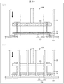
- FIG. 16 is a flow chart schematically showing an example of a thin-film deposition process for performing a thin-film deposition process in the thin-film deposition apparatus 100 shown in FIG. 12 including the alignment apparatus 170 shown in FIG. 17 to 20 are (a) cross-sectional views and (b) side views along the longitudinal direction of the substrate, schematically showing each part of the vapor deposition process in the vapor deposition apparatus shown in FIG.
- FIG. 17 (b), FIG. 18 (b), and FIG. 19 (b) these deflections are emphasized and illustrated so that the touch plate and the substrate are clearly bent. These are almost flat.
- the central portion of the substrate 120 is lowered and the substrate 120 is bent like a bowl. Further, as shown in FIG. 17B, the substrate 120 is supported from below by the tip portion 131a of the hook 131 at the peripheral portion. At this point, the substrate 120 is in a separated state in which the entire substrate 120 is separated from the mask sheet 111.
- the alignment device 170 performs alignment (step S32) after the substrate is carried in (step S31).
- the alignment device 170 that performs alignment first images the alignment marks 114 and 125 of the mask frame 112 and the substrate 120 with the camera 171 and determines the amount of deviation of the alignment mark 125 of the substrate 120 with respect to the alignment mark 114 of the vapor deposition mask 110 from the imaging data. Measure (step S33). Then, the first determination unit 181 determines whether the deviation amount is within the threshold range (first allowable range) (step S34).
- step S34 the alignment device 170 ends the alignment (step S32).
- step S32 the touch plate 101 presses the substrate 120 toward the mask sheet 111 by its own weight. Therefore, the touch plate 101 and the substrate 120 are bent downwardly in the direction of gravity together due to their own weight.
- “alignment” measures (i) the amount of deviation of the alignment mark 125 of the substrate 120 with respect to the alignment mark 114 of the vapor deposition mask 110 in a state where the substrate 120 is separated from the mask sheet 111 of the vapor deposition mask 110. , (Ii) It means that it is determined whether the deviation amount is within the threshold range, and (i) the deviation amount 0 is controlled as a target, and the substrate 120 is moved in the horizontal direction. Further, since the substrate 120 is lowered onto the vapor deposition mask 110 in a state where the substrate 120 is in contact with the touch plate 101 (steps S51, S56, S57), the substrate 120 also hits the touch plate 101 in the alignment (step S32). It is done in contact.
- the hook drive mechanism is such that the substrate 120 abuts on the mask sheet 111 only at the first end portion 126 in the longitudinal direction (first direction orthogonal to the elevating direction) of the substrate 120.
- the 132 drives the hook 131 that supports the substrate 120 (step S51, first driving step).
- step S51 first driving step.
- the second end portion 127 on the opposite side of the first end portion 126 and the intermediate portion 128 between the first end portion 126 and the second end portion 127 are separated from the mask sheet 111.
- the touch plate 101 presses the substrate 120, and at least the first end portion 101a of the touch plate 101 presses the first end portion 126 of the substrate 120 toward the mask sheet 111.
- the alignment device 170 confirms the alignment position of the first end portion 126 (step S52) in a state where only the first end portion 126 of the substrate 120 is in contact with the mask sheet 111. , 1st confirmation step) is executed.
- the alignment device 170 first captures the alignment marks 114 and 125 of the mask frame 112 and the substrate 120 on the first end 126 side with the camera 171, and from the imaging data, the alignment mark 114 of the substrate 120 with respect to the alignment mark 114 of the vapor deposition mask 1110.
- the amount of deviation of the alignment mark 125 is measured (step S53).
- the third determination unit 183 determines whether the deviation amount is within the threshold range (third allowable range) (step S54). If it is not within the threshold range (No), the substrate 120 and the touch plate 101 are pulled up to separate the substrate 120 from the vapor deposition mask 110 (step S55), and the process returns to alignment (step S32).
- the "alignment position confirmation for the first end portion 126" is performed on (i) the first end portion 126 of the substrate 120 in a state where only the first end portion 126 of the substrate 120 is in contact with the mask sheet 111. It means that the deviation amount of the provided alignment mark 125 with respect to the alignment mark 114 of the vapor deposition mask 110 is measured, and (ii) it is determined whether the deviation amount is within the threshold range.
- the threshold range for alignment position confirmation for the first end 126 is wider than the threshold range for alignment.
- step S54 when it was within the threshold range (Yes) in step S54, the intermediate portion 128 of the substrate 120 was gradually lowered from the first end portion 126 side to the second end portion 127 side.
- the hook drive mechanism 132 drives the hook 131 that supports the substrate 120 (step S56, the first half of the second drive step).
- step S56 the first half of the second drive step.
- the hook drive mechanism 132 (see FIG. 12) further drives the hook 131 supporting the substrate 120 so that the second end portion 127 of the substrate 120 comes into contact with the mask sheet 111 (step). S53, the latter half of the second drive step) is performed. As a result, the entire substrate 120 comes into contact with the mask sheet 111.
- the alignment device 170 confirms the alignment position of the second end portion 127 in a state where the entire substrate 120 is in contact with the mask sheet 111 (step S58, second confirmation step). ) Is executed.
- the alignment device 170 first captures the alignment marks 114 and 125 of the mask frame 112 and the substrate 120 on the second end 127 side with the camera 171, and from the imaging data, the alignment mark 114 of the substrate 120 with respect to the alignment mark 114 of the vapor deposition mask 110.
- the amount of deviation of the alignment mark 125 is measured (step S59).
- the fourth determination unit 184 determines whether the deviation amount is within the threshold range (fourth allowable range) (step S60). If it is not within the threshold range (No), the substrate 120 and the touch plate 101 are pulled up to separate the substrate 120 from the vapor deposition mask 110 (step S61), and the process returns to alignment (step S32).
- "confirmation of the alignment position for the second end 127" is performed in the state where both the first end 126 and the second end 127 of the substrate 120 are in contact with the mask sheet 111, and (i) the substrate 120. It means that the amount of deviation of the alignment mark 125 provided at the second end portion 127 of the vapor deposition mask 110 with respect to the alignment mark 114 is measured, and (ii) it is determined whether the deviation amount is within the threshold range.
- the threshold range in the alignment position confirmation for the second end 127 is wider than the threshold range in the alignment position confirmation for the first end 126 side.
- step S40 determines whether the substrate 120 is separated from the vapor deposition mask 110 by pulling up the substrate 120, the touch plate 101, and the magnet 140 (step S41), and the alignment (step S32) is returned.
- "confirmation of alignment position in close contact” means that (i) the amount of deviation of the alignment mark 125 of the substrate 120 with respect to the alignment mark 114 of the vapor deposition mask 110 while the substrate 120 is in close contact with the vapor deposition mask 110. It means measuring and (ii) determining whether the deviation amount is within the threshold range.
- the threshold range for the alignment position confirmation in the close contact state is wider than the threshold range for the alignment position confirmation for the second end portion 127.
- step S40 If it is within the threshold range in step S40 (Yes), the film is formed by depositing a vapor deposition material on the substrate 120 with the mask sheet 111 in close contact with the substrate 120 (step S42). After the vapor deposition is completed, magnet separation (step S43) and touch plate separation (step S44) are performed in this order, and the substrate 120 is lifted (step S45) to carry out the substrate 1120 (step S46).
- FIG. 21 is a block diagram showing another example of the schematic configuration of the alignment device 170 included in the vapor deposition device 100 shown in FIG.
- the alignment control mechanism 180 of the alignment device 170 shown in FIG. 21 confirms the alignment position of both the first determination unit 181 and the second determination unit 182, and the first end portion 126 and the second end portion 127 described later (step).
- a fifth determination unit 185 that performs the determination (step S64) in S62) and a control unit 186 are provided.
- FIG. 22 is a flow chart schematically showing another example of the vapor deposition process in the vapor deposition apparatus 100 shown in FIG. 12 including the alignment apparatus 170 shown in FIG. 21.
- the first end 126 and the second end Alignment position confirmation (S62) is performed for both parts 127.
- the alignment device 170 (see FIG. 21) is subjected to the substrate Alignment position confirmation (step S62, confirmation step) for both the first end portion 126 and the second end portion 127 is executed in a state where the entire 120 is in contact with the mask sheet 111.
- the alignment device 170 first captures the alignment marks 114 and 125 of the mask frames 112 and the substrate 120 on both ends 126 and 127 sides with the camera 171 and uses the imaging data to capture the alignment marks 114 of the substrate 120 with respect to the alignment marks 114 of the vapor deposition mask 110.
- the amount of deviation of the alignment mark 125 is measured (step S63). Then, the fifth determination unit 185 determines whether the deviation amount is within the threshold range (fifth allowable range) (step S64). If it is not within the threshold range (No), the substrate 120 and the touch plate 101 are pulled up to separate the substrate 120 from the vapor deposition mask 110 (step S65), return to the alignment (step S32), and step S35 to step. S37 is performed again.
- both the first end portion 126 and the second end portion 127 of the substrate 120 are in contact with the mask sheet 111.
- the threshold range in the alignment position confirmation for both the first end portion 126 and the second end portion 127 is wider than the threshold range in the alignment and narrower than the threshold range in the threshold range in the alignment position confirmation in the close contact state.
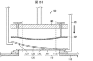
- FIG. 23 is a cross-sectional view taken along the longitudinal direction of the substrate 120, showing a case where the touch plate 101 does not press the substrate 120 in the substrate lowering step. As shown in FIG. 22, the substrate 120 may be gradually lowered along the longitudinal direction without being pressed by the touch plate 101.
- the example according to the first embodiment is not limited to this.
- the substrate 120 may be gradually lowered, for example, along the lateral direction.
- FIG. 24 is a cross-sectional view of the substrate 120 along the longitudinal direction showing an example of the schematic configuration of the vapor deposition apparatus 200 according to the second embodiment of the present invention.
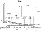
- FIG. 25 is a cross-sectional view taken along the longitudinal direction of the substrate 120, schematically showing a part of the substrate descent in the vapor deposition process in the vapor deposition apparatus 200 shown in FIG. 24.
- the vapor deposition apparatus 200 according to the second embodiment is different from the vapor deposition apparatus 100 according to the first embodiment, and has a touch plate 201 (first sheet member) and a touch plate 202 (second sheet member). It is equipped with two touch plates.
- the other configuration is that the thin-film deposition apparatus 200 according to the second embodiment is the same as the vapor deposition apparatus 100 according to the first embodiment.
- the two touch plates 201 and 202 are arranged along the longitudinal direction of the substrate 120.
- One touch plate 201 is one first sheet member arranged corresponding to the first end portion 126 of the substrate 120
- the other touch plate 202 is the second end portion 127 and the intermediate portion of the substrate 120. It is one second sheet member arranged corresponding to 128.
- One touch plate 201 may be elastically deformable without being substantially elastically deformed.
- the other touch plate 202 has a longer dimension than the one touch plate 201 in the longitudinal direction of the substrate 120 and is elastically deformable.
- the substrate 120 is first lowered so as to come into contact with the mask sheet 111 only at the first end portion 126. At this time, it is preferable that the touch plate 201 presses the first end portion 126 of the substrate 120 toward the mask sheet 111. Similar to the first embodiment, the substrate 120 is subsequently gradually lowered from the first end 126 side to the second end 127 side of the intermediate portion 128, and finally the second end portion 127. To.
- the example according to the second embodiment is not limited to this, and two touch plates 201 and 202 may be arranged along the lateral direction, for example, and gradually lowered along the arrangement direction.
- FIG. 26 is a cross-sectional view of the substrate 120 along the longitudinal direction showing an example of a schematic configuration of the vapor deposition apparatus 300 according to the third embodiment of the present invention.
- FIG. 25 is a cross-sectional view taken along the longitudinal direction of the substrate 120 which schematically shows an example of the vapor deposition process in the vapor deposition apparatus 300 shown in FIG.
- the vapor deposition apparatus 300 according to the third embodiment includes four touch plates 301, 302, 303, 303, unlike the vapor deposition apparatus 100, 200 according to the first and second embodiments described above.
- the other configurations of the vapor deposition apparatus 300 according to the third embodiment are the same as those of the vapor deposition apparatus 100 and 200 according to the first and second embodiments.
- the four touch plates 301, 302, 303, 303 are arranged along the longitudinal direction of the substrate 120.
- One touch plate 301 is one first sheet member arranged corresponding to the first end 126 of the substrate 120, and another touch plate 302 is attached to the second end 127 of the substrate 120. It is one second sheet member arranged correspondingly, and the remaining touch plates 303 and 303 (third sheet member) are two third sheets arranged corresponding to the intermediate portion 128 of the substrate 120. It is a member.
- the number of third sheet members arranged corresponding to the intermediate portion 128 is not limited to two, and may be one or three or more. Further, the third sheet members arranged corresponding to the intermediate portion 128 may have different widths in the longitudinal direction from each other.
- Each of the touch plates 301, 302, and 303 may be elastically deformable without being substantially elastically deformed.
- the dimensions of the touch plates 301, 302, 303 that is, the dimensions of the first sheet member, the second sheet member, and the third sheet member are the same as each other.
- the seat members having the same configuration can be used for any of the first seat member, the second seat member, and the third seat member.
- the substrate 120 is first lowered so as to come into contact with the mask sheet 111 only at the first end portion 126. At this time, it is preferable that the touch plate 301 presses the first end portion 126 of the substrate 120 toward the mask sheet 111. Similar to the first embodiment, the substrate 120 is subsequently gradually lowered from the first end 126 side to the second end 127 side of the intermediate portion 128, and finally the second end portion 127. To.
- the example according to the third embodiment is not limited to this, and the touch plates 301, 302, and 303 may be arranged along the lateral direction, for example, and gradually lowered along the arrangement direction.
- FIG. 28 is a cross-sectional view of the substrate 120 along the longitudinal direction showing an example of a schematic configuration of the vapor deposition apparatus 400 according to the fourth embodiment of the present invention.
- FIG. 29 is a cross-sectional view taken along the longitudinal direction of the substrate 120, schematically showing an example of substrate descent in the vapor deposition step in the vapor deposition apparatus 400 shown in FIG. 28.
- the vapor deposition apparatus 400 according to the fourth embodiment includes three touch plates 401, 402, 403, unlike the vapor deposition apparatus 100, 200, 300 according to the above-described first to third embodiments.
- Other configurations are the same as the vapor deposition apparatus 400 according to the fourth embodiment as the vapor deposition apparatus 100, 200, 300 according to the first to third embodiments.
- the three touch plates 401, 402, and 403 are arranged along the longitudinal direction of the substrate 120.
- One touch plate 401 is one first sheet member arranged corresponding to the first end 126 of the substrate 120, and another touch plate 402 is on the second end 127 of the substrate 120. It is one second sheet member arranged correspondingly, and the remaining touch plate 403 is one third sheet member arranged corresponding to the entire intermediate portion 128 of the substrate 120.
- the touch plate 401 arranged corresponding to the first end portion 126 may be elastically deformable without being substantially elastically deformed.
- the touch plate 402 arranged corresponding to the second end portion 127 may be elastically deformable without being substantially elastically deformed.
- the touch plate 403 arranged corresponding to the intermediate portion 128 has a longer dimension than the touch plates 401 and 402 in the longitudinal direction of the substrate 120 and is elastically deformable.
- the substrate 120 is first lowered so as to come into contact with the mask sheet 111 only at the first end portion 126. At this time, it is preferable that the touch plate 401 presses the first end portion 126 of the substrate 120 toward the mask sheet 111. Similar to the first embodiment, the substrate 120 is subsequently gradually lowered from the first end 126 side to the second end 127 side of the intermediate portion 128, and finally the second end portion 127. To.
- the example according to the fourth embodiment is not limited to this, and the touch plates 401, 402, 403 may be arranged along the lateral direction, for example, and may be gradually lowered along the arrangement direction.
- the thin-film deposition apparatus is arranged between a thin-film deposition source, a thin-film deposition mask having a mask sheet and a mask frame, a magnet for bringing the mask sheet into close contact with the substrate, and the substrate and the magnet.
- a vapor deposition apparatus including a touch plate, an elevating device for raising and lowering the substrate with respect to the vapor deposition mask, and an alignment device for aligning the vapor deposition mask with the substrate.
- a plurality of support members provided around the substrate and in contact with a non-deposited region other than the surface to be vapor-deposited of the substrate to support the substrate, and the plurality of support members connected to the plurality of support members.
- a drive mechanism for driving the members independently of each other in the elevating direction of the substrate is provided, and the drive mechanism is such that the substrate is pressed by the touch plate and only one end of the substrate is vapor-deposited. While driving the support member so as to abut the mask and pressing the substrate with the touch plate, the other end gradually hits the vapor deposition mask toward the other end of the substrate. The support member is driven so as to be in contact with the support member.
- the touch plate may be configured to be one sheet member that can be elastically deformed.
- the vapor deposition apparatus may have a configuration in which the touch plate is a plurality of sheet members arranged along the longitudinal direction thereof in the above aspect 1.
- the vapor deposition apparatus may have a configuration in which the dimensions of each of the plurality of sheet members in the longitudinal direction are the same as each other in the above aspect 3.
- the plurality of sheet members are the first sheet member and the first sheet member arranged on the one end portion and the other end portion side of the substrate, respectively.
- the configuration may include two seat members.
- the dimension of the second sheet member in the longitudinal direction may be longer than the dimension of the first sheet member in the longitudinal direction. Good.
- the second sheet member may be a single sheet member that can be elastically deformed.
- the plurality of sheet members are the first sheet member and the first sheet member arranged on the one end portion and the other end portion side of the substrate, respectively.
- the configuration may further include a two-seat member and a third seat member arranged between the first seat member and the second seat member.
- the dimensions of the third sheet member in the longitudinal direction are the dimensions of the first sheet member and the second sheet member in the longitudinal direction. It may be a longer configuration than that.
- the three sheet members may be configured to be one elastically deformable sheet member.
- the alignment device in any one of the above aspects 1 to 10, includes an imaging unit provided above the magnet in the elevating direction, and the substrate is , The one end and the other end are provided with a substrate alignment mark, the vapor deposition mask is provided with a mask alignment mark corresponding to the substrate alignment mark, and the touch plate is provided with the imaging unit.
- the substrate alignment mark and the mask alignment mark may be configured to have an imaging through hole for imaging.
- the thin-film deposition apparatus may have a structure in which the magnet is formed with a visible hole superimposing on the image pickup through hole of the touch plate.
- the vapor deposition apparatus further includes a magnet driving mechanism for driving the magnet in the elevating direction with respect to the substrate in any one of the above aspects 1 to 12, and the touch plate is the touch plate. It may be configured to be connected to the magnet so as to be movable in the elevating direction with respect to the magnet.
- the thin-film deposition apparatus hangs the touch plate movably from the magnet so that the touch plate can press the substrate toward the mask sheet by its own weight. It may be a lowered configuration.
- the mask frame is provided with a plurality of recesses capable of accommodating the tip portions of the plurality of support members. It may be configured.
- the method for manufacturing a display device is a method for manufacturing a display device having a substrate, which comprises a vapor deposition step of performing a vapor deposition process on the substrate by using a vapor deposition mask.
- the first driving step of driving the support member supporting the substrate so that only one end of the substrate abuts on the vapor deposition mask while the substrate is pressed by the touch plate, and the touch plate A second driving step of driving the support member so that the other end of the substrate gradually abuts on the vapor deposition mask while pressing the substrate is included.
- one end of the substrate abuts on the thin-film deposition mask between the first driving step and the second driving step.
- the first confirmation step of confirming the alignment position between the substrate alignment mark provided at one end and the mask alignment mark provided on the vapor deposition mask is executed, and after the second drive step, Second, the alignment position between the substrate alignment mark provided on the other end and the mask alignment mark provided on the vapor deposition mask is confirmed in a state where the other end of the substrate is in contact with the vapor deposition mask. It may be a method of executing the confirmation process.
- one end and the other end of the substrate are in contact with the vapor deposition mask after the second driving step.
- Display device 100, 200, 300, 400 Thin film deposition equipment 101 Touch plate 106 Through hole for imaging 110 Vapor deposition mask 111 Mask sheet 112 Mask frame 114 Alignment mark (mask alignment mark) 115 Recess 120 Substrate 125 Alignment mark (Board alignment mark) 126 1st end 127 2nd end 128 Intermediate 130 Lifting device 131 Hook (support member) 131a Tip 132 Hook drive mechanism (drive mechanism) 140 Magnet 142 Magnet drive mechanism 143 Visual recognition hole 171 Camera (imaging unit) 160 Thin-film deposition sources 201, 301, 401 Touch plate (first sheet member) 202, 302, 402 Touch plate (second sheet member) 303, 403 Touch plate (third sheet member)
Landscapes
- Chemical & Material Sciences (AREA)
- Chemical Kinetics & Catalysis (AREA)
- Engineering & Computer Science (AREA)
- Materials Engineering (AREA)
- Mechanical Engineering (AREA)
- Metallurgy (AREA)
- Organic Chemistry (AREA)
- Electroluminescent Light Sources (AREA)
Abstract
Selon l'invention, dans ce dispositif de dépôt (100), un substrat (120) est abaissé de sorte que seule sa première section d'extrémité (126) entre en contact avec une feuille de masquage (111) puis, que la totalité du substrat (120) entre progressivement en contact avec la feuille de masquage (111), en partant de la première section d'extrémité (126) vers une seconde section d'extrémité (127). Lorsque seule la première section d'extrémité (126) entre en contact avec la feuille de masquage (111), au moins une partie (101a) d'une plaque de contact (101) presse le substrat (120) vers la feuille de masquage (111).
Priority Applications (1)
| Application Number | Priority Date | Filing Date | Title |
|---|---|---|---|
| PCT/JP2019/009531 WO2020183552A1 (fr) | 2019-03-08 | 2019-03-08 | Dispositif de dépôt et procédé de fabrication de dispositif d'affichage |
Applications Claiming Priority (1)
| Application Number | Priority Date | Filing Date | Title |
|---|---|---|---|
| PCT/JP2019/009531 WO2020183552A1 (fr) | 2019-03-08 | 2019-03-08 | Dispositif de dépôt et procédé de fabrication de dispositif d'affichage |
Publications (1)
| Publication Number | Publication Date |
|---|---|
| WO2020183552A1 true WO2020183552A1 (fr) | 2020-09-17 |
Family
ID=72426197
Family Applications (1)
| Application Number | Title | Priority Date | Filing Date |
|---|---|---|---|
| PCT/JP2019/009531 Ceased WO2020183552A1 (fr) | 2019-03-08 | 2019-03-08 | Dispositif de dépôt et procédé de fabrication de dispositif d'affichage |
Country Status (1)
| Country | Link |
|---|---|
| WO (1) | WO2020183552A1 (fr) |
Cited By (1)
| Publication number | Priority date | Publication date | Assignee | Title |
|---|---|---|---|---|
| CN113652633A (zh) * | 2021-08-13 | 2021-11-16 | 京东方科技集团股份有限公司 | 掩模板框架、掩模板组件及其制备方法 |
Citations (6)
| Publication number | Priority date | Publication date | Assignee | Title |
|---|---|---|---|---|
| JPS632150B2 (fr) * | 1981-10-16 | 1988-01-18 | Nippon Electric Co | |
| JP2008007857A (ja) * | 2006-06-02 | 2008-01-17 | Sony Corp | アライメント装置、アライメント方法および表示装置の製造方法 |
| JP2008108596A (ja) * | 2006-10-26 | 2008-05-08 | Seiko Epson Corp | マスク蒸着法、およびマスク蒸着装置 |
| JP2008156686A (ja) * | 2006-12-22 | 2008-07-10 | Seiko Epson Corp | マスクおよびマスク蒸着装置 |
| JP2010157526A (ja) * | 2008-12-26 | 2010-07-15 | Ulvac Japan Ltd | アラインメント機能付き基板載置装置と、その基板載置装置を有する成膜装置 |
| JP2018105853A (ja) * | 2016-12-27 | 2018-07-05 | 株式会社アルバック | ギャップ計測方法 |
-
2019
- 2019-03-08 WO PCT/JP2019/009531 patent/WO2020183552A1/fr not_active Ceased
Patent Citations (6)
| Publication number | Priority date | Publication date | Assignee | Title |
|---|---|---|---|---|
| JPS632150B2 (fr) * | 1981-10-16 | 1988-01-18 | Nippon Electric Co | |
| JP2008007857A (ja) * | 2006-06-02 | 2008-01-17 | Sony Corp | アライメント装置、アライメント方法および表示装置の製造方法 |
| JP2008108596A (ja) * | 2006-10-26 | 2008-05-08 | Seiko Epson Corp | マスク蒸着法、およびマスク蒸着装置 |
| JP2008156686A (ja) * | 2006-12-22 | 2008-07-10 | Seiko Epson Corp | マスクおよびマスク蒸着装置 |
| JP2010157526A (ja) * | 2008-12-26 | 2010-07-15 | Ulvac Japan Ltd | アラインメント機能付き基板載置装置と、その基板載置装置を有する成膜装置 |
| JP2018105853A (ja) * | 2016-12-27 | 2018-07-05 | 株式会社アルバック | ギャップ計測方法 |
Cited By (2)
| Publication number | Priority date | Publication date | Assignee | Title |
|---|---|---|---|---|
| CN113652633A (zh) * | 2021-08-13 | 2021-11-16 | 京东方科技集团股份有限公司 | 掩模板框架、掩模板组件及其制备方法 |
| CN113652633B (zh) * | 2021-08-13 | 2023-10-27 | 京东方科技集团股份有限公司 | 掩模板框架、掩模板组件及其制备方法 |
Similar Documents
| Publication | Publication Date | Title |
|---|---|---|
| JP6993804B2 (ja) | マスク組立体、表示装置の製造装置、表示装置の製造方法、及び表示装置 | |
| JP6211873B2 (ja) | 有機el表示装置及び有機el表示装置の製造方法 | |
| US11227553B2 (en) | Display device | |
| US11626449B2 (en) | Display device and method for producing display device | |
| WO2016082393A1 (fr) | Substrat d'affichage à diode électroluminescente organique et son procédé de fabrication, et appareil d'affichage | |
| JP2016054085A (ja) | 表示装置および表示装置の製造方法 | |
| US20180307369A1 (en) | Display device | |
| KR20210120175A (ko) | 마스크 어셈블리, 표시 장치의 제조장치, 및 표시 장치의 제조방법 | |
| JP7124208B2 (ja) | 蒸着装置、および表示装置の製造方法 | |
| US12161021B2 (en) | Display device, mask, and method for manufacturing display device | |
| JP2025083384A (ja) | マスク組立体とその製造方法、及び表示装置の製造装置並びに表示装置の製造方法 | |
| JP2019003040A (ja) | 表示装置 | |
| US11416108B2 (en) | Display device | |
| KR20150002119A (ko) | 유기전계 발광소자 및 이의 제조 방법 | |
| JP2022087011A (ja) | 電界発光表示装置 | |
| WO2020183552A1 (fr) | Dispositif de dépôt et procédé de fabrication de dispositif d'affichage | |
| KR102122528B1 (ko) | 플렉서블 유기발광다이오드 표시장치 및 그 제조방법 | |
| WO2019186901A1 (fr) | Procédé de production de dispositif d'affichage | |
| US10600668B2 (en) | Adsorption device, conveyance device, and EL device manufacturing device | |
| US12310191B2 (en) | Display device and manufacturing method for display device | |
| US12501803B2 (en) | Display device and method of manufacturing the same | |
| WO2020161829A1 (fr) | Dispositif d'affichage | |
| US10777633B2 (en) | Display device, display device manufacturing method, and display device manufacturing apparatus | |
| US11640771B2 (en) | Display device | |
| US20210134930A1 (en) | Display device |
Legal Events
| Date | Code | Title | Description |
|---|---|---|---|
| 121 | Ep: the epo has been informed by wipo that ep was designated in this application |
Ref document number: 19918733 Country of ref document: EP Kind code of ref document: A1 |
|
| NENP | Non-entry into the national phase |
Ref country code: DE |
|
| 122 | Ep: pct application non-entry in european phase |
Ref document number: 19918733 Country of ref document: EP Kind code of ref document: A1 |
|
| NENP | Non-entry into the national phase |
Ref country code: JP |