WO2020183603A1 - Dispositif semi-conducteur à contact par pression - Google Patents
Dispositif semi-conducteur à contact par pression Download PDFInfo
- Publication number
- WO2020183603A1 WO2020183603A1 PCT/JP2019/009939 JP2019009939W WO2020183603A1 WO 2020183603 A1 WO2020183603 A1 WO 2020183603A1 JP 2019009939 W JP2019009939 W JP 2019009939W WO 2020183603 A1 WO2020183603 A1 WO 2020183603A1
- Authority
- WO
- WIPO (PCT)
- Prior art keywords
- electrode
- intermediate electrode
- chip
- semiconductor device
- pressure
- Prior art date
- Legal status (The legal status is an assumption and is not a legal conclusion. Google has not performed a legal analysis and makes no representation as to the accuracy of the status listed.)
- Ceased
Links
Images


Classifications
-
- H—ELECTRICITY
- H10—SEMICONDUCTOR DEVICES; ELECTRIC SOLID-STATE DEVICES NOT OTHERWISE PROVIDED FOR
- H10W—GENERIC PACKAGES, INTERCONNECTIONS, CONNECTORS OR OTHER CONSTRUCTIONAL DETAILS OF DEVICES COVERED BY CLASS H10
- H10W72/00—Interconnections or connectors in packages
-
- H—ELECTRICITY
- H10—SEMICONDUCTOR DEVICES; ELECTRIC SOLID-STATE DEVICES NOT OTHERWISE PROVIDED FOR
- H10W—GENERIC PACKAGES, INTERCONNECTIONS, CONNECTORS OR OTHER CONSTRUCTIONAL DETAILS OF DEVICES COVERED BY CLASS H10
- H10W76/00—Containers; Fillings or auxiliary members therefor; Seals
- H10W76/10—Containers or parts thereof
- H10W76/12—Containers or parts thereof characterised by their shape
- H10W76/13—Containers comprising a conductive base serving as an interconnection
- H10W76/138—Containers comprising a conductive base serving as an interconnection having another interconnection being formed by a cover plate parallel to the conductive base, e.g. sandwich type
-
- H—ELECTRICITY
- H10—SEMICONDUCTOR DEVICES; ELECTRIC SOLID-STATE DEVICES NOT OTHERWISE PROVIDED FOR
- H10W—GENERIC PACKAGES, INTERCONNECTIONS, CONNECTORS OR OTHER CONSTRUCTIONAL DETAILS OF DEVICES COVERED BY CLASS H10
- H10W90/00—Package configurations
-
- H—ELECTRICITY
- H10—SEMICONDUCTOR DEVICES; ELECTRIC SOLID-STATE DEVICES NOT OTHERWISE PROVIDED FOR
- H10D—INORGANIC ELECTRIC SEMICONDUCTOR DEVICES
- H10D12/00—Bipolar devices controlled by the field effect, e.g. insulated-gate bipolar transistors [IGBT]
- H10D12/411—Insulated-gate bipolar transistors [IGBT]
- H10D12/441—Vertical IGBTs
- H10D12/461—Vertical IGBTs having non-planar surfaces, e.g. having trenches, recesses or pillars in the surfaces of the emitter, base or collector regions
- H10D12/481—Vertical IGBTs having non-planar surfaces, e.g. having trenches, recesses or pillars in the surfaces of the emitter, base or collector regions having gate structures on slanted surfaces, on vertical surfaces, or in grooves, e.g. trench gate IGBTs
-
- H—ELECTRICITY
- H10—SEMICONDUCTOR DEVICES; ELECTRIC SOLID-STATE DEVICES NOT OTHERWISE PROVIDED FOR
- H10W—GENERIC PACKAGES, INTERCONNECTIONS, CONNECTORS OR OTHER CONSTRUCTIONAL DETAILS OF DEVICES COVERED BY CLASS H10
- H10W72/00—Interconnections or connectors in packages
- H10W72/071—Connecting or disconnecting
- H10W72/073—Connecting or disconnecting of die-attach connectors
- H10W72/07331—Connecting techniques
- H10W72/07336—Soldering or alloying
-
- H—ELECTRICITY
- H10—SEMICONDUCTOR DEVICES; ELECTRIC SOLID-STATE DEVICES NOT OTHERWISE PROVIDED FOR
- H10W—GENERIC PACKAGES, INTERCONNECTIONS, CONNECTORS OR OTHER CONSTRUCTIONAL DETAILS OF DEVICES COVERED BY CLASS H10
- H10W72/00—Interconnections or connectors in packages
- H10W72/30—Die-attach connectors
- H10W72/351—Materials of die-attach connectors
- H10W72/352—Materials of die-attach connectors comprising metals or metalloids, e.g. solders
-
- H—ELECTRICITY
- H10—SEMICONDUCTOR DEVICES; ELECTRIC SOLID-STATE DEVICES NOT OTHERWISE PROVIDED FOR
- H10W—GENERIC PACKAGES, INTERCONNECTIONS, CONNECTORS OR OTHER CONSTRUCTIONAL DETAILS OF DEVICES COVERED BY CLASS H10
- H10W72/00—Interconnections or connectors in packages
- H10W72/90—Bond pads, in general
- H10W72/921—Structures or relative sizes of bond pads
- H10W72/926—Multiple bond pads having different sizes
-
- H—ELECTRICITY
- H10—SEMICONDUCTOR DEVICES; ELECTRIC SOLID-STATE DEVICES NOT OTHERWISE PROVIDED FOR
- H10W—GENERIC PACKAGES, INTERCONNECTIONS, CONNECTORS OR OTHER CONSTRUCTIONAL DETAILS OF DEVICES COVERED BY CLASS H10
- H10W72/00—Interconnections or connectors in packages
- H10W72/90—Bond pads, in general
- H10W72/941—Dispositions of bond pads
- H10W72/944—Dispositions of multiple bond pads
-
- H—ELECTRICITY
- H10—SEMICONDUCTOR DEVICES; ELECTRIC SOLID-STATE DEVICES NOT OTHERWISE PROVIDED FOR
- H10W—GENERIC PACKAGES, INTERCONNECTIONS, CONNECTORS OR OTHER CONSTRUCTIONAL DETAILS OF DEVICES COVERED BY CLASS H10
- H10W72/00—Interconnections or connectors in packages
- H10W72/90—Bond pads, in general
- H10W72/951—Materials of bond pads
- H10W72/952—Materials of bond pads comprising metals or metalloids, e.g. PbSn, Ag or Cu
-
- H—ELECTRICITY
- H10—SEMICONDUCTOR DEVICES; ELECTRIC SOLID-STATE DEVICES NOT OTHERWISE PROVIDED FOR
- H10W—GENERIC PACKAGES, INTERCONNECTIONS, CONNECTORS OR OTHER CONSTRUCTIONAL DETAILS OF DEVICES COVERED BY CLASS H10
- H10W90/00—Package configurations
- H10W90/701—Package configurations characterised by the relative positions of pads or connectors relative to package parts
- H10W90/731—Package configurations characterised by the relative positions of pads or connectors relative to package parts of die-attach connectors
- H10W90/736—Package configurations characterised by the relative positions of pads or connectors relative to package parts of die-attach connectors between a chip and a stacked lead frame, conducting package substrate or heat sink
Definitions
- the present invention relates to a pressure welding type semiconductor device.
- Power modules for electric power convert or control high voltage of several kilovolts and large current of several kiloamperes, and further increase in capacity is required.
- a plurality of semiconductor elements are mounted in parallel in a large-capacity power module.
- the demand for power modules has been increasing in harsh environments such as offshore wind power generation, and power modules with high reliability and redundancy are required.
- a pressure welding type semiconductor device is attracting attention instead of the conventional bonding type.
- a plurality of semiconductor chips are mounted on the pressure welding type semiconductor device, and metal blocks are provided above and below the semiconductor chips as intermediate electrodes. Further, by being pressed from above and below the intermediate electrode via the common electrode plate, electrical contact inside the apparatus is maintained.
- a buffer region is provided between the active region and the terminal region of the IGBT chip, a pedestal portion higher than the active region is provided in the buffer region, and the outer peripheral portion of the surface intermediate electrode is provided.
- a method is disclosed in which the pedestal portion is crushed and pressurized, and the central portion of the block contacts the active region. This method can prevent the outer peripheral portion of the surface intermediate electrode from coming into contact with the surface electrode of the semiconductor chip.
- the module since it is necessary to increase the chip size in order to newly provide the buffer area, the module becomes large and the productivity is lowered.
- a step of forming a pedestal on the buffer region is required, which complicates the manufacturing process.
- the present invention has been made to solve the above problems, and suppresses electrical contact between the outer peripheral portion of the intermediate electrode and the surface electrode of the semiconductor chip without increasing the area of the semiconductor chip. With the goal.
- a plurality of semiconductor chips having a first main electrode and a second main electrode on the front surface and the back surface, a first intermediate electrode facing the first main electrode of the semiconductor chip, and a first A first common electrode plate provided on the side opposite to the surface of the intermediate electrode facing the first main electrode and a second common electrode plate provided facing the second main electrode are provided, and the first intermediate electrode is provided with a second common electrode plate.
- the surface facing the first main electrode is smaller than the surface facing the first intermediate electrode of the first main electrode, and has a protection region on the outer periphery and a connection region surrounded by the protection region.
- a plurality of first conductor films partially formed in a connection region, and a first insulating film formed in a region in which the first conductor film is not formed and a protective region in the connection region.
- the outer peripheral portion of the first intermediate electrode is not increased in the area of the semiconductor chip. Can be prevented from electrically contacting the outer peripheral portion of the semiconductor chip.
- FIG. 1 It is sectional drawing of the pressure welding type semiconductor device of a prerequisite technology. It is a figure which shows the structure of the contact part of the anode intermediate electrode and the diode chip in Embodiment 1.
- FIG. It is a figure which shows the structure of the contact part of the emitter intermediate electrode and the IGBT chip in Embodiment 1.
- FIG. It is a top view of the contact surface of the surface intermediate electrode with respect to the semiconductor chip in the modification of Embodiment 1.
- FIG. It is a top view of the contact surface of the surface intermediate electrode with respect to the semiconductor chip in the modification of Embodiment 1.
- FIG. It is a top view of the contact surface of the surface intermediate electrode with respect to the semiconductor chip in the modification of Embodiment 1.
- FIG. 1 It is a top view of the contact surface of the surface intermediate electrode with respect to the semiconductor chip in the modification of Embodiment 1.
- FIG. 2 is a top view of the contact surface of the surface intermediate electrode with respect to the semiconductor chip in the modification of Embodiment 1.
- FIG. It is a figure which shows the structure of the contact part between the emitter intermediate electrode and the IGBT chip in Embodiment 2.
- FIG. It is a figure which shows the mounting example of the pressure welding type semiconductor device of Embodiment 2.
- FIG. It is sectional drawing of the IGBT chip along the AA'line of FIG. It is a figure which shows the structure of the contact part of the anode intermediate electrode and the diode chip in Embodiment 3.
- FIG. It is sectional drawing of the diode chip along the line BB'of FIG. It is a top view of the IGBT chip of Embodiment 4.
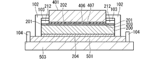
- FIG. 1 is a cross-sectional view of the pressure welding type semiconductor device 100 of the prerequisite technology.
- the pressure welding type semiconductor device 100 includes a plurality of IGBT (Insulated Gate Bipolar Transistor) chips 200 and a plurality of diode chips 300.
- IGBT Insulated Gate Bipolar Transistor
- diode chips 300 an IGBT chip and a diode chip are given as examples of semiconductor chips.
- the front surface of the IGBT chip 200 is provided with a terminal region 201, an emitter electrode 202 as a front surface electrode, and a gate pad 203, and a collector electrode 204 is provided on the back surface.
- the emitter electrode 202 is also referred to as a first main electrode
- the collector electrode 204 is also referred to as a second main electrode.
- An emitter intermediate electrode 401 is provided directly above the emitter electrode 202. In other words, the emitter intermediate electrode 401 faces the emitter electrode 202 of the IGBT chip 200.
- a collector intermediate electrode 501 is provided directly below the collector electrode 204.
- the front surface of the diode chip 300 is provided with an anode electrode 301 and a terminal region 303, which are surface electrodes, and the back surface is provided with a cathode electrode 302.
- An anode intermediate electrode 402 is provided directly above the anode electrode 301.
- a cathode intermediate electrode 502 is provided directly below the cathode electrode 302.
- the emitter intermediate electrode 401 and the anode intermediate electrode 402 are collectively referred to as a front surface intermediate electrode 400
- the collector intermediate electrode 501 and the cathode intermediate electrode 502 are collectively referred to as a back surface intermediate electrode 500.
- the surface intermediate electrode 400 is also referred to as a first intermediate electrode.
- the front surface intermediate electrode 400 and the back surface intermediate electrode 500 are collectively referred to as an intermediate electrode.
- the emitter common electrode plate 403 and the collector common electrode plate 503 are collectively referred to as a common electrode plate.
- the IGBT chips 200 and the diode chips 300 are connected in parallel via the intermediate electrode, and the IGBT chip 200 and the diode chip 300 are connected in antiparallel. That is, the diode chip 300 functions as a freewheeling diode (FWD).
- the semiconductor chip may come into direct contact with the collector common electrode plate 503, and in this case, the back surface intermediate electrode 500 is unnecessary.
- a control terminal 601 provided with a spring pin or the like is connected to the gate pad 203 of the IGBT chip 200.
- the control terminal 601 is drawn out of the housing and connected to a gate drive circuit (not shown).
- the common electrode plate is made of a metal plate such as copper.
- the intermediate electrode is made of a metal such as copper, tungsten or molybdenum.
- the back surface intermediate electrode 500 is fixed to the collector electrode 204 and the cathode electrode 302 with, for example, solder.
- a plating film such as nickel may be formed on the contact surface between the intermediate electrode and the semiconductor chip in order to reduce the contact resistance.
- the surface intermediate electrode 400 is shown as a mere metal block in FIG. 1, it may have a structure in which the metal block and the spring above it are integrated. With such a structure, the spring absorbs the variation in pressure applied between the semiconductor chips.
- the pressure applied to the surface intermediate electrode 400 is concentrated on the outermost circumference of the metal block.
- the contact area between the surface electrode and the surface intermediate electrode 400 of the semiconductor chip gradually increases from the outer circumference to the inside as the pressure increases. If the pressure applied to each semiconductor chip varies, the contact resistance between the surface electrode and the surface intermediate electrode 400 of each semiconductor chip varies, causing non-uniform current, and thus the reliability of the pressure welding type semiconductor device 100 deteriorates. To do.
- the pressure-welding semiconductor device of the first embodiment is the pressure-welding semiconductor device 100 of the prerequisite technology shown in FIG. 1, in which the contact portion between the surface intermediate electrode 400 and the semiconductor chip is devised, and other than that.
- the configuration of is the same as that of the pressure welding type semiconductor device 100.
- the configuration of the contact portion between the surface intermediate electrode 400 and the semiconductor chip in the pressure contact type semiconductor device of the first embodiment will be described with reference to FIGS. 2 and 3.
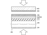
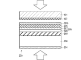
- FIG. 2 shows the configuration on the diode chip 300 side.
- FIG. 2 shows a contact surface of the anode intermediate electrode 402 with the diode chip 300 in the upper part, a cross-sectional view of the anode intermediate electrode 402 in the middle part, and a cross-sectional view of the diode chip 300 in the lower part.
- the dotted line in FIG. 2 shows the positional relationship between the anode intermediate electrode 402 and the diode chip 300.
- the contact surface of the anode intermediate electrode 402 with respect to the diode chip 300 is smaller than that of the anode electrode 301 of the diode chip 300.
- the anode intermediate electrode 402 is arranged inside the anode electrode 301. As long as this condition is satisfied, an arbitrary size and shape is adopted for the contact surface of the anode intermediate electrode 402 with respect to the diode chip 300.
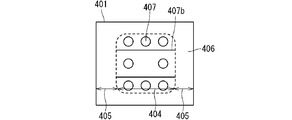
- the contact surface of the surface intermediate electrode 400 with respect to the semiconductor chip is divided into a protective region 405 on the outer peripheral portion and a connection region 404 inside the protective region 405.
- a plurality of conductor films 407 are formed in the connection region 404, and the connection region 404 realizes electrical contact between the surface intermediate electrode 400 and the semiconductor chip.
- the width 405b of the protection region 405 is preferably about 5 to 15% of the length of a piece of the metal block constituting the anode intermediate electrode 402.
- the protective region 405 and the region of the connection region 404 where the conductor film 407 is not formed are covered with the insulating film 406.
- the conductor film 407 is preferably arranged point-symmetrically with respect to the center of gravity of the contact surface of the anode intermediate electrode 402 with respect to the diode chip 300.
- FIG. 3 shows the configuration on the IGBT chip 200 side.
- FIG. 3 shows the contact surface of the emitter intermediate electrode 401 with the IGBT chip 200 in the upper part, the cross-sectional view of the emitter intermediate electrode 401 in the middle part, and the sectional view of the IGBT chip 200 in the lower part.
- the dotted line in FIG. 3 shows the positional relationship between the emitter intermediate electrode 401 and the IGBT chip 200.
- the contact surface of the emitter intermediate electrode 401 with respect to the IGBT chip 200 is smaller than that of the emitter electrode 202 of the IGBT chip 200.
- the emitter intermediate electrode 401 is arranged inside the emitter electrode 202. As long as this condition is satisfied, an arbitrary size and shape is adopted for the contact surface of the emitter intermediate electrode 401 with respect to the IGBT chip 200.
- the contact surface of the emitter intermediate electrode 401 with respect to the IGBT chip 200 is divided into a protection region 405 and a connection region 404.
- the arrangement of the conductor film 407 in the protection region 405 is the same for the anode intermediate electrode 402 and the emitter intermediate electrode 401.
- the pressure applied to the surface intermediate electrode 400 is small, the pressure is applied only to the outer peripheral portion of the surface intermediate electrode 400. However, as the pressure increases, the pressure is gradually applied to the inside of the surface intermediate electrode 400.
- the pressure contact type semiconductor device of the first embodiment since the contact surface of the surface intermediate electrode 400 with respect to the semiconductor chip is configured as shown in FIGS. 2 and 3, each conductor film 407 and the semiconductor chip are pressed in a well-balanced manner and come into contact with each other. Variations in resistance are suppressed.
- the insulating film 406 is formed by depositing oxides or nitrides by, for example, sputtering or vapor deposition. Alternatively, the insulating film 406 is formed by a method such as spraying an insulating paint or resin or spin coating with a spin coater. At this time, the region where the conductor film 407 is formed is protected by a metal mask, tape, or the like so that the insulating film is not formed in the region. Alternatively, after forming the insulating film as a whole, the insulating film in the region where the conductor film 407 is formed is removed.
- the conductor film 407 is formed by forming a metal film by sputtering, vapor deposition, or the like. Alternatively, a thick film metal may be formed by electrolytic plating to form a conductor film 407.
- the pressure welding type semiconductor device of the first embodiment is a plurality of semiconductor chips having a first main electrode and a second main electrode on the front surface and the back surface, respectively, and a first intermediate electrode facing the first main electrode of the semiconductor chip.
- the facing surface of the surface intermediate electrode 400 with the first main electrode is smaller than the facing surface of the first main electrode with the surface intermediate electrode 400, and the connection region 404 surrounded by the protective region 405 and the protection region 405 on the outer periphery.
- the conductor film 407 which is a plurality of first conductor films partially formed in the connection region 404, and the region of the connection region 404 where the conductor film 407 is not formed and the protection region 405
- the insulating film 406, which is the first insulating film formed in the above, is provided.
- the surface intermediate electrode 400 conducts with the first main electrode of the semiconductor chip in the connection region 404 instead of the protection region 405 of the outer peripheral portion, so that the semiconductor chip It is possible to prevent the outer peripheral portion of the surface intermediate electrode 400 from electrically contacting the outer peripheral portion of the semiconductor chip without increasing the area.
- the conductor film 407 is arranged point-symmetrically with respect to the center of gravity of the contact surface on the contact surface of the surface intermediate electrode 400 with respect to the semiconductor chip, that is, the facing surface, between each surface intermediate electrode 400 and the semiconductor chip. Contact resistance is made uniform. As a result, variations in the current applied between the semiconductor chips in the pressure-welded semiconductor device are suppressed, and the reliability of the pressure-welded semiconductor device is improved.
- the insulating film 406 can also function as a cushioning material on the outer peripheral portion of the surface intermediate electrode 400 to which a high pressure is applied. As a result, it is possible to suppress the introduction of cracks into the semiconductor chip even when a high pressure is applied, and to improve the productivity and reliability of the pressure-welded semiconductor device.
- a soft resin such as polyimide
- the outer peripheral portion of the surface intermediate electrode 400 is covered with the insulating film 406, a positional deviation occurs between the semiconductor chip and the surface intermediate electrode 400, and the surface intermediate electrode 400 is the gate pad 203 or the termination regions 201 and 303. Since no electrical short circuit occurs even when the is pressed, defects during assembly can be reduced.
- a buffer plate is provided so as to face the emitter electrode of the IGBT chip.
- the cushioning plate of the prior document 2 includes a plurality of electrode members and an insulating member that separates the electrode members. This buffer plate is considered to correspond to the surface intermediate electrode in the first embodiment.
- the common point between the pressure-welded semiconductor device of the first embodiment and the prior document 2 is that the energizable region of the surface intermediate electrode is limited. However, there is no description about the arrangement and area of the conductor region in the surface intermediate electrode in the prior document 2.
- the pressure of the surface intermediate electrode is generally applied intensively to the outer peripheral portion, so that the IGBT chip
- the outer peripheral portion and the conductor portion of the surface intermediate electrode are in preferential contact.
- the energization region is limited to the outer peripheral portion, the electric resistance between the collector and the emitter electrodes increases, and the loss of the power module increases.
- the energized region is excessively limited, the current is concentrated and heat is generated, which may damage the IGBT chip.
- the central portion of the IGBT chip also comes into contact with the emitter electrode of the surface intermediate electrode.
- the contact area between the IGBT chip and the surface intermediate electrode increases, and the resistance between the collector and the emitter electrode increases. descend. Since the resistance of the IGBT chip changes depending on the pressure, the amount of current applied between the IGBT chips in the pressure contact type semiconductor device becomes non-uniform, and the reliability of the device deteriorates.
- the conduction region is limited to the region where a uniform pressure is applied, a stable collector-emitter electrode resistance can be obtained regardless of the pressure variation. As a result, a highly reliable pressure-welded semiconductor device can be obtained without increasing the loss.
- the conductor member and the insulating member are made of different materials, and one surface intermediate electrode is formed by combining them.
- the insulating region and the conductor region are formed by patterning the surface of the surface intermediate electrode 400. Therefore, since the number of parts does not increase, there is an advantage that the manufacturing is easy and the degree of freedom in designing the conductor region is high.
- FIGS. 4 to 8 Examples of deformation of the contact surface of the surface intermediate electrode 400 with respect to the semiconductor chip are shown in FIGS. 4 to 8.
- the conductor film 407 was not formed on the center of gravity of the surface intermediate electrode 400.
- the conductor film 407 may be formed on the center of gravity of the surface intermediate electrode 400.
- the number of divisions of the conductor film 407 is arbitrary, and may be, for example, 4 as shown in FIG. 5, 16 as shown in FIG. 6, and 3 as shown in FIG. It is preferable that the sizes of the conductor films 407 are the same, but the above-mentioned effects can be obtained even if they are not necessarily the same.
- the shape of the conductor film 407 does not have to be circular, and may be rectangular, for example, as shown in FIG. Further, the conductor films 407 having a plurality of shapes may be used in combination.
- an IGBT and a freewheeling diode are used as the semiconductor chip mounted on the pressure welding type semiconductor device 100, but the type of the semiconductor chip is not limited to this.
- a MOSFET Metal-Oxide-Semiconductor Field-Effect Transistor
- the number of the IGBT chips 200 and the diode chips 300 can be arbitrarily changed according to the rated current of the module. The number of IGBT chips 200 and diode chips 300 does not have to be the same. For example, the number of IGBT chips 200 may be twice the number of diode chips 300. Any material such as silicon, gallium nitride, silicon carbide, aluminum nitride, gallium oxide or diamond is used for the substrate of the semiconductor chip depending on the application.
- a reverse conduction IGBT (RC-IGBT: Reverse-conducting IGBT) may be used.
- RC-IGBT Reverse-conducting IGBT
- the structure shown in FIG. 3 can be applied to the structure of the contact surface of the surface intermediate electrode 400 with respect to the reverse conductive IGBT chip.
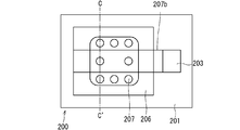
- Embodiment 2 In the pressure contact type semiconductor device of the first embodiment, the configuration of the contact portion between the emitter intermediate electrode 401 and the IGBT chip 200 is changed. Hereinafter, the configuration of the contact portion between the emitter intermediate electrode 401 and the IGBT chip 200 in the pressure contact type semiconductor device of the second embodiment will be described with reference to FIGS. 9 to 11.
- the upper part shows the contact surface of the emitter intermediate electrode 401 with the IGBT chip 200
- the lower part is a top view of the IGBT chip 200.
- the IGBT chip 200 is provided with a gate wiring 205 which is a control wiring electrically separated from the emitter electrode 202 in order to supply a gate current from the gate pad 203 to each cell.
- the gate wiring 205 is a low resistance wiring layer formed on the surface of the chip via SiO 2 or the like on the semiconductor substrate.
- the gate wiring 205 may be, for example, a metal film such as aluminum, a polysilicon film in which impurities are heavily doped, or a laminated film thereof.
- two gate wiring 205s are drawn in the lower part of FIG. 9, the number of gate wirings 205 can be arbitrarily changed according to the chip size.
- the gate pad 203 is arranged at an arbitrary position in the IGBT chip 200.
- the broken line circle drawn in the emitter electrode 202 at the lower part of FIG. 9 indicates the position where the conductor film 407 at the upper part of FIG. 9 comes into contact.
- the pressure-welding semiconductor device of the second embodiment is different from the pressure-welding semiconductor device of the first embodiment in that the conductor film 407 is formed so as not to come into contact with the gate wiring 205 of the IGBT chip 200. In order to realize this structure, the alignment accuracy of the emitter intermediate electrode 401 and the IGBT chip 200 must be sufficiently high.
- FIG. 10 shows an implementation example of a pressure welding type semiconductor device that realizes high alignment accuracy.
- the IGBT chip 200 is fixed to the collector intermediate electrode 501 with solder.
- the collector intermediate electrode guide 104 is provided on the collector common electrode plate 503, and the collector intermediate electrode 501 is arranged on the collector common electrode plate 503 along the collector intermediate electrode guide 104. That is, the position of the collector intermediate electrode 501 in the module is defined by the collector intermediate electrode guide 104.
- a protective film 212 of the terminal region 201 is formed on the outer periphery of the IGBT chip 200 with polyimide or the like.
- the chip guide 102 is placed on the protective film 212 and fixed with the adhesive 103.
- the tip guide 102 is made of, for example, a silicone resin.
- FIG. 11 is a schematic cross-sectional view of the IGBT chip 200 passing through the gate wiring 205.
- the IGBT chip 200 has a configuration in which a semiconductor layer 208, an insulating film 210, a polysilicon layer 209, a gate metal layer 211, and an insulating film 206 are laminated in this order.
- the polysilicon layer 209 and the gate metal layer 211 correspond to the gate wiring 205.
- the insulating films 206 and 210 are second insulating films that cover the gate wiring 205.
- the insulating film 210 is made of SiO 2 or the like, and the insulating film 206 is made of SiN or the like.
- the gate wiring 205 is a low resistance wiring layer above the trench, and in a planar type MOSFET or IGBT, a low voltage electrically connected to the gate electrode of each transistor. It is a resistance wiring layer.
- the conductor film 407 is formed at a position that does not overlap with the gate wiring 205 in a plan view. Therefore, even if a crack is introduced into the insulating film 206, the gate metal layer 211 is electrically separated from the emitter intermediate electrode 401 by the insulating film 406. Therefore, a high pressure can be applied to the pressure-welded semiconductor device, the contact resistance between the semiconductor chip and the intermediate electrode is reduced, and a low-loss pressure-welded semiconductor device is realized. Further, since a high pressure can be applied between the common electrode plates, the gap between the IGBT chip 200 and the intermediate electrode is reduced. Therefore, when the IGBT chip 200 is short-circuited and broken, it is suppressed that an arc discharge occurs in the gap between the IGBT chip 200 and the intermediate electrode and the breaking occurs, and the reliability of the module is improved.
- the pressure-welding semiconductor device of the third embodiment is the pressure-welding semiconductor device of the first embodiment in which the configuration of the contact portion between the surface intermediate electrode 400 and the semiconductor chip is changed.
- the configuration of the contact portion between the surface intermediate electrode 400 and the semiconductor chip in the pressure contact type semiconductor device of the third embodiment will be described with reference to FIGS. 12 to 15.
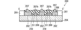
- FIG. 12 and 13 show the configuration of the pressure welding type semiconductor device of the third embodiment on the IGBT side.
- FIG. 12 shows a top view of the contact surface of the emitter intermediate electrode 401 with respect to the IGBT chip 200, a cross-sectional view of the emitter intermediate electrode 401, and a top view of the IGBT chip 200.
- FIG. 13 is a cross-sectional view of the IGBT chip 200 along the AA'line of FIG.
- the gate wiring 205 is provided radially from the center of the cell region of the IGBT chip 200.
- the emitter electrode 202 is radially divided by the gate wiring 205, specifically by the insulating films 206 and 210 covering the gate wiring 205, and is formed into a plurality of island-shaped electrodes as shown in FIG. That is, the insulating films 206 and 210 are third insulating films that divide the emitter electrode 202 into a plurality of islands. Most of the upper surface of each of the divided emitter electrodes 202 is covered with an insulating film 206 made of silicon dioxide or silicon nitride, and a conductor film 207 which is a second conductor film is formed in the remaining portion.
- the conductor film 207 is connected to the lower emitter electrode 202.
- the conductor film 207 is preferably arranged point-symmetrically with respect to the center of gravity of the contact surface on the contact surface of the IGBT chip 200 with respect to the emitter intermediate electrode 401. Further, as shown in FIG. 12, it is preferable that the conductor film 207 is evenly arranged on each emitter electrode 202 divided by the gate wiring 205. Evenly arranged means that the surface areas of the conductor films 207 formed on the emitter electrodes 202 are equal.
- a conductor film 407 is formed at a position corresponding to the conductor film 207 in the connection region 404 on the contact surface of the emitter intermediate electrode 401 with respect to the IGBT chip 200, and comes into contact with the conductor film 207.
- An insulating film 406 is formed at other positions on the contact surface.
- FIG. 14 and 15 show the configuration on the diode side of the pressure welding type semiconductor device of the third embodiment.
- FIG. 14 shows a top view of the contact surface of the anode intermediate electrode 402 with respect to the diode chip 300, a cross-sectional view of the anode intermediate electrode 402, and a top view of the diode chip 300.
- FIG. 15 is a cross-sectional view of the diode chip 300 along the line BB'of FIG.
- the anode electrode 301 is radially divided from the center by an insulating film 306 made of silicon dioxide or the like to form a plurality of island-shaped electrodes.
- Most of the upper surface of the anode electrode 301 is covered with an insulating film 304 made of silicon dioxide or silicon nitride, and a conductor film 305 is formed on the remaining portion. That is, the insulating films 304 and 306 function as a third insulating film that divides the anode electrode 301 into a plurality of islands.
- the conductor film 305 is connected to the lower anode electrode 301.
- the conductor film 305 is preferably arranged point-symmetrically with respect to the center of gravity of the contact surface on the contact surface of the diode chip 300 with respect to the anode intermediate electrode 402. Further, as shown in FIG. 14, it is preferable that the conductor film 305 is evenly arranged on each anode electrode 301 divided by the insulating film 306. Evenly arranged means that the surface areas of the conductor films 305 at each anode electrode 301 are equal.
- a conductor film 407 is formed at a position in contact with the conductor film 207 in the connection region 404, and an insulating film 406 is formed at a position other than that.
- the surface electrode of the semiconductor chip is divided into a plurality of island-shaped electrodes, and a conductor film is uniformly formed on each of the divided surface electrodes.
- the contact resistance between each of the divided surface electrodes and the surface intermediate electrode 400 becomes uniform.
- the current is applied to the surface electrode having a small resistance and the temperature rises as compared with the other surface electrodes.
- the resistance of the surface electrode increases, so that the current non-uniformity in the semiconductor chip is naturally reduced.
- the pressure-welding semiconductor device according to the fourth embodiment is the pressure-welding semiconductor device according to the second embodiment, in which the configuration of the contact portion between the emitter intermediate electrode 401 and the IGBT chip 200 is changed.
- the configuration of the contact portion between the emitter intermediate electrode 401 and the IGBT chip 200 in the pressure contact type semiconductor device of the fourth embodiment will be described with reference to FIGS. 16 to 20.
- the present embodiment can also be combined with the third embodiment.
- FIG. 16 is a top view of the IGBT chip 200.
- FIG. 17 is a cross-sectional view of the IGBT chip 200 along the CC'line of FIG.
- FIG. 18 is a schematic cross-sectional view of the IGBT chip 200 passing through the gate wiring 205.
- FIG. 19 is a top view of the contact surface of the emitter intermediate electrode 401 with respect to the IGBT chip 200.
- the pressure-welding semiconductor device of the fourth embodiment is the pressure-welding semiconductor device of the second embodiment, in which the IGBT chip 200 is provided with the conductor film 207b which is the third conductor film, and the emitter intermediate electrode 401 is provided with the conductor film 407b. Is. Other than these, the configuration of the pressure welding type semiconductor device of the fourth embodiment is the same as that of the pressure welding type semiconductor device of the second embodiment.
- the conductor film 207b is provided on the outermost surface of the region where the gate wiring 205 of the IGBT chip 200 is formed.
- the conductor film 407b is provided in a region of the connection region 404 of the emitter intermediate electrode 401 that comes into contact with the conductor film 207b. That is, the conductor film 207b and the conductor film 407b come into contact with each other.
- the IGBT chip 200 has a configuration in which a semiconductor layer 208, an insulating film 210, a polysilicon layer 209, a gate metal layer 211, an insulating film 206, and a conductor film 207b are laminated in this order.
- the insulating film 206 is made of silicon dioxide or silicon nitride.
- the conductor film 207b is formed of, for example, a single film such as nickel or gold or a laminated film.
- the emitter intermediate electrode 401 and the IGBT chip 200 are required to have high positional accuracy. Therefore, it is preferable to position the emitter intermediate electrode 401 by the same method as in FIG.
- the pressure welding type semiconductor device of the fourth embodiment has been described as a modification to the pressure welding type semiconductor device of the second embodiment.
- this embodiment is also applicable to the third embodiment.
- the conductor film 207b which is a relatively soft metal film on the gate wiring 205 by forming the conductor film 207b which is a relatively soft metal film on the gate wiring 205, the unevenness existing in the emitter intermediate electrode 401 is absorbed by the conductor film 207b and locally on the gate wiring 205. High pressure is prevented from being applied to the wire. As a result, the insulating film 206 on the gate wiring 205 is damaged by the pressure, and the gate metal layer 211 is prevented from coming into contact with the emitter intermediate electrode 401. As a result, the reliability of the pressure-welded semiconductor device is improved, damage during manufacturing is suppressed, and productivity is improved.
- the conductor film 207b becomes the emitter potential.
- the gate metal layer 211 becomes a gate potential due to the gate current supplied from the gate pad 203.
- the equivalent circuit diagram of the IGBT chip 200 at this time is shown in FIG.
- a power supply voltage Vcc and a gate-emitter voltage Vge are applied to the IGBT element 701.
- An internal gate resistor Rg1 and / or an external gate resistor Rg2 are connected to the gate electrode.
- the gate-collector capacitance Cgt and the gate-emitter capacitance Cge are connected as parasitic capacitances.
- the gate metal layer 211 and the conductor film 207b form a parallel plate capacitor via the insulating film 206.
- the gate wiring 205 has a parasitic resistance, as shown by the broken line in FIG. 20, a parasitic snubber circuit 702 is formed between the gate and the emitter in parallel with the main gate wiring 205. As a result, the oscillation of the gate voltage can be suppressed.
- the capacitance of the parasitic snubber circuit 702 can be controlled by the film thickness of the insulating film 206.
- each embodiment can be freely combined, and each embodiment can be appropriately modified or omitted.
- the present invention has been described in detail, the above description is exemplary in all embodiments and the invention is not limited thereto. It is understood that a myriad of variations not illustrated can be envisioned without departing from the scope of the invention.
Landscapes
- Die Bonding (AREA)
- Electrodes Of Semiconductors (AREA)
Abstract
Le but de la présente invention est de supprimer un contact électrique entre une partie périphérique externe d'une électrode intermédiaire et une électrode de surface d'une puce semi-conductrice sans augmenter l'aire de la puce semi-conductrice. La surface d'une première électrode intermédiaire (400) opposée à une première électrode principale (202, 301) est plus petite que la surface de la première électrode principale (202, 301) opposée à la première électrode intermédiaire (400) et présente une zone de protection (405) dans la partie périphérique extérieure et une zone de raccordement (404) entourée par la zone de protection (405). Ce dispositif semi-conducteur à contact par pression comporte : une pluralité de premiers films conducteurs (407) partiellement formés dans la zone de raccordement (404) ; et un premier film isolant (406) formé dans la zone de protection (405) et dans une zone de la zone de raccordement (404) où les premiers films conducteurs (407) ne sont pas formés.
Priority Applications (5)
| Application Number | Priority Date | Filing Date | Title |
|---|---|---|---|
| JP2021504673A JP7080392B2 (ja) | 2019-03-12 | 2019-03-12 | 圧接型半導体装置 |
| PCT/JP2019/009939 WO2020183603A1 (fr) | 2019-03-12 | 2019-03-12 | Dispositif semi-conducteur à contact par pression |
| US17/424,912 US11742313B2 (en) | 2019-03-12 | 2019-03-12 | Pressure-contact semiconductor device |
| CN201980093656.3A CN113544828B (zh) | 2019-03-12 | 2019-03-12 | 压接型半导体装置 |
| DE112019007008.8T DE112019007008B4 (de) | 2019-03-12 | 2019-03-12 | Druckkontakt-halbleitereinheit |
Applications Claiming Priority (1)
| Application Number | Priority Date | Filing Date | Title |
|---|---|---|---|
| PCT/JP2019/009939 WO2020183603A1 (fr) | 2019-03-12 | 2019-03-12 | Dispositif semi-conducteur à contact par pression |
Publications (1)
| Publication Number | Publication Date |
|---|---|
| WO2020183603A1 true WO2020183603A1 (fr) | 2020-09-17 |
Family
ID=72427322
Family Applications (1)
| Application Number | Title | Priority Date | Filing Date |
|---|---|---|---|
| PCT/JP2019/009939 Ceased WO2020183603A1 (fr) | 2019-03-12 | 2019-03-12 | Dispositif semi-conducteur à contact par pression |
Country Status (5)
| Country | Link |
|---|---|
| US (1) | US11742313B2 (fr) |
| JP (1) | JP7080392B2 (fr) |
| CN (1) | CN113544828B (fr) |
| DE (1) | DE112019007008B4 (fr) |
| WO (1) | WO2020183603A1 (fr) |
Citations (2)
| Publication number | Priority date | Publication date | Assignee | Title |
|---|---|---|---|---|
| WO1998043301A1 (fr) * | 1997-03-26 | 1998-10-01 | Hitachi, Ltd. | Dispositif plat a semi-conducteur et convertisseur de courant utilisant ce dernier |
| WO2016189953A1 (fr) * | 2015-05-26 | 2016-12-01 | 三菱電機株式会社 | Dispositif à semi-conducteur à contact par pression |
Family Cites Families (5)
| Publication number | Priority date | Publication date | Assignee | Title |
|---|---|---|---|---|
| JPH11186299A (ja) * | 1997-12-17 | 1999-07-09 | Hitachi Ltd | 加圧接触型半導体装置及びこれを用いた電力変換器 |
| CN1236982A (zh) * | 1998-01-22 | 1999-12-01 | 株式会社日立制作所 | 压力接触型半导体器件及其转换器 |
| JP2003264266A (ja) | 2002-03-08 | 2003-09-19 | Fuji Electric Co Ltd | 半導体装置 |
| JP3994945B2 (ja) | 2003-08-26 | 2007-10-24 | 日産自動車株式会社 | 半導体装置および半導体装置の製造方法 |
| JP5203032B2 (ja) | 2008-04-28 | 2013-06-05 | 本田技研工業株式会社 | 圧接型半導体装置 |
-
2019
- 2019-03-12 CN CN201980093656.3A patent/CN113544828B/zh active Active
- 2019-03-12 US US17/424,912 patent/US11742313B2/en active Active
- 2019-03-12 WO PCT/JP2019/009939 patent/WO2020183603A1/fr not_active Ceased
- 2019-03-12 DE DE112019007008.8T patent/DE112019007008B4/de active Active
- 2019-03-12 JP JP2021504673A patent/JP7080392B2/ja active Active
Patent Citations (2)
| Publication number | Priority date | Publication date | Assignee | Title |
|---|---|---|---|---|
| WO1998043301A1 (fr) * | 1997-03-26 | 1998-10-01 | Hitachi, Ltd. | Dispositif plat a semi-conducteur et convertisseur de courant utilisant ce dernier |
| WO2016189953A1 (fr) * | 2015-05-26 | 2016-12-01 | 三菱電機株式会社 | Dispositif à semi-conducteur à contact par pression |
Also Published As
| Publication number | Publication date |
|---|---|
| JP7080392B2 (ja) | 2022-06-03 |
| CN113544828B (zh) | 2024-12-06 |
| US11742313B2 (en) | 2023-08-29 |
| US20220108972A1 (en) | 2022-04-07 |
| JPWO2020183603A1 (ja) | 2021-10-21 |
| DE112019007008B4 (de) | 2025-01-16 |
| CN113544828A (zh) | 2021-10-22 |
| DE112019007008T5 (de) | 2021-11-18 |
Similar Documents
| Publication | Publication Date | Title |
|---|---|---|
| US11171122B2 (en) | Semiconductor device | |
| US9165871B2 (en) | Semiconductor unit and semiconductor device using the same | |
| US7514780B2 (en) | Power semiconductor device | |
| US10861833B2 (en) | Semiconductor device | |
| US9899328B2 (en) | Power semiconductor module | |
| US6734551B2 (en) | Semiconductor device | |
| KR102100859B1 (ko) | 양면 냉각 파워 모듈 및 이의 제조방법 | |
| US10727209B2 (en) | Semiconductor device and semiconductor element with improved yield | |
| US11923266B2 (en) | Semiconductor module circuit structure | |
| JP3319569B2 (ja) | 圧接型半導体装置 | |
| US20180158762A1 (en) | Semiconductor device | |
| US5874774A (en) | Flat package semiconductor device | |
| JP7080392B2 (ja) | 圧接型半導体装置 | |
| JP2000058820A (ja) | パワー半導体素子及びパワーモジュール | |
| JP3973832B2 (ja) | 圧接型半導体装置 | |
| JP3612226B2 (ja) | 半導体装置及び半導体モジュール | |
| JP2000012845A (ja) | 半導体装置 | |
| US20030107049A1 (en) | Semiconductor device and its manufacturing method | |
| JP4218479B2 (ja) | 半導体装置 | |
| US20260068748A1 (en) | Semiconductor device | |
| US20250239560A1 (en) | Semiconductor device | |
| US20240096720A1 (en) | Semiconductor module having a double-sided heat dissipation structure and A Method for fabricating the same | |
| US20230028808A1 (en) | Semiconductor device | |
| US20240120307A1 (en) | Semiconductor device | |
| US10847489B2 (en) | Semiconductor device |
Legal Events
| Date | Code | Title | Description |
|---|---|---|---|
| 121 | Ep: the epo has been informed by wipo that ep was designated in this application |
Ref document number: 19918823 Country of ref document: EP Kind code of ref document: A1 |
|
| ENP | Entry into the national phase |
Ref document number: 2021504673 Country of ref document: JP Kind code of ref document: A |
|
| 122 | Ep: pct application non-entry in european phase |
Ref document number: 19918823 Country of ref document: EP Kind code of ref document: A1 |