WO2020184016A1 - Élément d'imagerie, procédé de fabrication d'élément d'imagerie et dispositif d'imagerie - Google Patents
Élément d'imagerie, procédé de fabrication d'élément d'imagerie et dispositif d'imagerie Download PDFInfo
- Publication number
- WO2020184016A1 WO2020184016A1 PCT/JP2020/004774 JP2020004774W WO2020184016A1 WO 2020184016 A1 WO2020184016 A1 WO 2020184016A1 JP 2020004774 W JP2020004774 W JP 2020004774W WO 2020184016 A1 WO2020184016 A1 WO 2020184016A1
- Authority
- WO
- WIPO (PCT)
- Prior art keywords
- electrode
- photoelectric conversion
- electron blocking
- blocking layer
- conversion layer
- Prior art date
- Legal status (The legal status is an assumption and is not a legal conclusion. Google has not performed a legal analysis and makes no representation as to the accuracy of the status listed.)
- Ceased
Links
Images



Classifications
-
- H—ELECTRICITY
- H10—SEMICONDUCTOR DEVICES; ELECTRIC SOLID-STATE DEVICES NOT OTHERWISE PROVIDED FOR
- H10K—ORGANIC ELECTRIC SOLID-STATE DEVICES
- H10K39/00—Integrated devices, or assemblies of multiple devices, comprising at least one organic radiation-sensitive element covered by group H10K30/00
- H10K39/30—Devices controlled by radiation
- H10K39/32—Organic image sensors
-
- H—ELECTRICITY
- H04—ELECTRIC COMMUNICATION TECHNIQUE
- H04N—PICTORIAL COMMUNICATION, e.g. TELEVISION
- H04N23/00—Cameras or camera modules comprising electronic image sensors; Control thereof
- H04N23/20—Cameras or camera modules comprising electronic image sensors; Control thereof for generating image signals from infrared radiation only
- H04N23/21—Cameras or camera modules comprising electronic image sensors; Control thereof for generating image signals from infrared radiation only from near infrared [NIR] radiation
-
- H—ELECTRICITY
- H04—ELECTRIC COMMUNICATION TECHNIQUE
- H04N—PICTORIAL COMMUNICATION, e.g. TELEVISION
- H04N25/00—Circuitry of solid-state image sensors [SSIS]; Control thereof
- H04N25/70—SSIS architectures; Circuits associated therewith
-
- H—ELECTRICITY
- H10—SEMICONDUCTOR DEVICES; ELECTRIC SOLID-STATE DEVICES NOT OTHERWISE PROVIDED FOR
- H10F—INORGANIC SEMICONDUCTOR DEVICES SENSITIVE TO INFRARED RADIATION, LIGHT, ELECTROMAGNETIC RADIATION OF SHORTER WAVELENGTH OR CORPUSCULAR RADIATION
- H10F39/00—Integrated devices, or assemblies of multiple devices, comprising at least one element covered by group H10F30/00, e.g. radiation detectors comprising photodiode arrays
- H10F39/10—Integrated devices
- H10F39/12—Image sensors
-
- H—ELECTRICITY
- H10—SEMICONDUCTOR DEVICES; ELECTRIC SOLID-STATE DEVICES NOT OTHERWISE PROVIDED FOR
- H10K—ORGANIC ELECTRIC SOLID-STATE DEVICES
- H10K30/00—Organic devices sensitive to infrared radiation, light, electromagnetic radiation of shorter wavelength or corpuscular radiation
- H10K30/30—Organic devices sensitive to infrared radiation, light, electromagnetic radiation of shorter wavelength or corpuscular radiation comprising bulk heterojunctions, e.g. interpenetrating networks of donor and acceptor material domains
- H10K30/353—Organic devices sensitive to infrared radiation, light, electromagnetic radiation of shorter wavelength or corpuscular radiation comprising bulk heterojunctions, e.g. interpenetrating networks of donor and acceptor material domains comprising blocking layers, e.g. exciton blocking layers
-
- H—ELECTRICITY
- H10—SEMICONDUCTOR DEVICES; ELECTRIC SOLID-STATE DEVICES NOT OTHERWISE PROVIDED FOR
- H10K—ORGANIC ELECTRIC SOLID-STATE DEVICES
- H10K30/00—Organic devices sensitive to infrared radiation, light, electromagnetic radiation of shorter wavelength or corpuscular radiation
- H10K30/80—Constructional details
- H10K30/81—Electrodes
- H10K30/82—Transparent electrodes, e.g. indium tin oxide [ITO] electrodes
-
- H—ELECTRICITY
- H10—SEMICONDUCTOR DEVICES; ELECTRIC SOLID-STATE DEVICES NOT OTHERWISE PROVIDED FOR
- H10K—ORGANIC ELECTRIC SOLID-STATE DEVICES
- H10K30/00—Organic devices sensitive to infrared radiation, light, electromagnetic radiation of shorter wavelength or corpuscular radiation
- H10K30/80—Constructional details
- H10K30/87—Light-trapping means
-
- Y—GENERAL TAGGING OF NEW TECHNOLOGICAL DEVELOPMENTS; GENERAL TAGGING OF CROSS-SECTIONAL TECHNOLOGIES SPANNING OVER SEVERAL SECTIONS OF THE IPC; TECHNICAL SUBJECTS COVERED BY FORMER USPC CROSS-REFERENCE ART COLLECTIONS [XRACs] AND DIGESTS
- Y02—TECHNOLOGIES OR APPLICATIONS FOR MITIGATION OR ADAPTATION AGAINST CLIMATE CHANGE
- Y02E—REDUCTION OF GREENHOUSE GAS [GHG] EMISSIONS, RELATED TO ENERGY GENERATION, TRANSMISSION OR DISTRIBUTION
- Y02E10/00—Energy generation through renewable energy sources
- Y02E10/50—Photovoltaic [PV] energy
- Y02E10/549—Organic PV cells
-
- Y—GENERAL TAGGING OF NEW TECHNOLOGICAL DEVELOPMENTS; GENERAL TAGGING OF CROSS-SECTIONAL TECHNOLOGIES SPANNING OVER SEVERAL SECTIONS OF THE IPC; TECHNICAL SUBJECTS COVERED BY FORMER USPC CROSS-REFERENCE ART COLLECTIONS [XRACs] AND DIGESTS
- Y02—TECHNOLOGIES OR APPLICATIONS FOR MITIGATION OR ADAPTATION AGAINST CLIMATE CHANGE
- Y02P—CLIMATE CHANGE MITIGATION TECHNOLOGIES IN THE PRODUCTION OR PROCESSING OF GOODS
- Y02P70/00—Climate change mitigation technologies in the production process for final industrial or consumer products
- Y02P70/50—Manufacturing or production processes characterised by the final manufactured product
Definitions
- the present disclosure relates to an image sensor, a method for manufacturing the image sensor, and an image sensor.
- the image pickup device includes a first electrode, a second electrode, and a photoelectric conversion layer arranged between them. At least one selected from the first electrode and the second electrode is a transparent electrode.
- the photoelectric conversion layer absorbs the incident light to generate electron-hole pairs.
- An electron blocking layer may be arranged between the first electrode and the photoelectric conversion layer.
- the electron blocking layer is a layer through which holes easily pass and electrons do not easily pass through.
- Patent Document 1 describes an image sensor provided with a buffer layer arranged between the first electrode and the photoelectric conversion layer.
- the image sensor has the characteristic that the dark current, which is the leakage current in the dark, is large. Since the leakage current lowers the S / N ratio (signal to noise ratio) of the image sensor, it is required to reduce the leakage current.
- the image sensor according to one aspect of the present disclosure is With the first electrode With the second electrode A photoelectric conversion layer arranged between the first electrode and the second electrode and converting light into electric charges, An electron blocking layer containing chromium oxide and carbon, which is arranged between the first electrode and the photoelectric conversion layer and suppresses the transfer of electrons from the first electrode to the photoelectric conversion layer. To be equipped.
- FIG. 1A is a cross-sectional view of an image sensor according to an embodiment of the present disclosure.
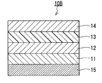
- FIG. 1B is a cross-sectional view of the image pickup device according to the modified example.
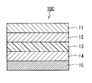
- FIG. 1C is a cross-sectional view of an image sensor according to another modification.
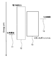
- FIG. 2 is an exemplary energy band diagram of the image sensor shown in FIG. 1A.
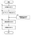
- FIG. 3 is a flowchart showing a manufacturing process of the image pickup device shown in FIG. 1A.
- FIG. 4 is a diagram showing an example of a circuit of an imaging device according to an embodiment of the present disclosure.
- FIG. 5 is a cross-sectional view of a unit pixel in the image pickup apparatus according to the embodiment of the present disclosure.
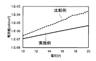
- FIG. 6 is a graph showing the relationship between the voltage applied to the second electrode and the detected current value.
- the image sensor is used in an image pickup device such as a CMOS (Complementary Metal Oxide Semiconductor) image sensor, for example.
- CMOS Complementary Metal Oxide Semiconductor
- a voltage may be applied to the photoelectric conversion layer regardless of whether or not the photoelectric conversion layer is irradiated with light. In this case, electrons flow from the electrodes to the photoelectric conversion layer, and the S / N ratio of the sensor decreases.
- the image sensor according to the first aspect of the present disclosure is With the first electrode With the second electrode A photoelectric conversion layer arranged between the first electrode and the second electrode and converting light into electric charges, An electron blocking layer containing chromium oxide and carbon, which is arranged between the first electrode and the photoelectric conversion layer and suppresses the transfer of electrons from the first electrode to the photoelectric conversion layer. Is equipped with.
- the electron blocking layer may include a plurality of layers.
- the carbon may be contained in the layer containing the oxide of chromium among the plurality of layers.
- the photoelectric conversion layer may contain a photoelectric conversion material, and the photoelectric conversion material may be an organic material. According to the second aspect, it is possible to form the photoelectric conversion layer by directly applying the solution containing the photoelectric conversion material onto the electron blocking layer.
- the photoelectric conversion layer may absorb near infrared light having a wavelength of 780 nm to 2000 nm to generate the charge.
- the image sensor of the third aspect can be used for a sensor that detects near infrared light.
- the absorption peak wavelength of the photoelectric conversion layer may be in the wavelength region of 780 nm to 2000 nm.
- the image sensor of the fourth aspect can be used for a sensor that detects near infrared light.
- the second electrode is such that light is incident from the second electrode toward the photoelectric conversion layer.
- the photoelectric conversion layer, the electron blocking layer, and the first electrode may be arranged in this order. According to this arrangement, the attenuation of the incident light in the electron blocking layer can be suppressed.
- the manufacturing method according to the sixth aspect of the present disclosure is a manufacturing method of an image sensor.
- the image pickup device is arranged between the first electrode, the second electrode, the photoelectric conversion layer arranged between the first electrode and the second electrode, and between the first electrode and the photoelectric conversion layer.
- the electron blocking layer contains chromium oxide and carbon, and contains
- the manufacturing method is Forming the electron blocking layer and Preparing an organic solution containing a photoelectric conversion material and To form the photoelectric conversion layer by applying the organic solution to the electron blocking layer, including.
- the electron blocking layer is hardly damaged.
- a photoelectric conversion layer can be easily formed by applying an organic solution and drying.
- the electron blocking layer may be formed by a metal-organic compound decomposition method.
- the electron blocking layer containing chromium oxide and carbon can be formed with high productivity.
- the image sensor according to the eighth aspect of the present disclosure is with any one of the image sensors of the first to fifth aspects, With the charge storage region electrically connected to the first electrode or the second electrode, A charge detection circuit electrically connected to the charge storage region and Is equipped with.
- the leakage current in the dark can be reduced, improvement in image quality, particularly, improvement in image quality when the amount of light is low can be expected.
- all or part of a circuit, unit, device, member or part, or all or part of a functional block in a block diagram is, for example, a semiconductor device, a semiconductor integrated circuit (IC), or an LSI (range scale integration). ) Can be performed by one or more electronic circuits.
- the LSI or IC may be integrated on one chip, or may be configured by combining a plurality of chips.
- the functional blocks other than the memory element may be integrated on one chip.
- it is called LSI or IC, but the name changes depending on the degree of integration, and it may be called system LSI, VLSI (very large scale integration), or ULSI (ultra large scale integration).
- a Field Programmable Gate Array (FPGA) programmed after the LSI is manufactured, or a reconfigurable logistic device capable of reconfiguring the junction relationship inside the LSI or setting up the circuit partition inside the LSI can also be used for the same purpose.
- FPGA Field Programmable Gate Array
- circuits, units, devices, members or parts can be performed by software processing.
- the software is recorded on a non-temporary recording medium such as one or more ROMs, optical disks, hard disk drives, etc., and when the software is executed by a processor, the functions identified by the software It is performed by a processor and peripherals.
- the system or device may include one or more non-temporary recording media on which the software is recorded, a processor, and the required hardware devices, such as an interface.
- FIG. 1A shows a cross section of the image sensor 10A according to the embodiment of the present disclosure.
- the image pickup device 10A includes a first electrode 11, an electron blocking layer 12, a photoelectric conversion layer 13, and a second electrode 14.
- the photoelectric conversion layer 13 is arranged between the first electrode 11 and the second electrode 14.
- the electron blocking layer 12 is arranged between the first electrode 11 and the photoelectric conversion layer 13.
- the electron blocking layer 12 is in contact with the first electrode 11 and the photoelectric conversion layer 13.
- the photoelectric conversion layer 13 is in contact with the electron blocking layer 12 and the second electrode 14.
- the first electrode 11, the electron blocking layer 12, the photoelectric conversion layer 13 and the second electrode 14 are laminated in this order.
- the second electrode 14, the photoelectric conversion layer 13, the electron blocking layer 12, and the first electrode 11 are arranged in this order so that light is incident from the second electrode 14 toward the photoelectric conversion layer 13. According to this arrangement, the attenuation of the incident light in the electron blocking layer 12 can be suppressed.
- the image sensor 10A is used, for example, as a part of the pixels of the image sensor.
- the image sensor 10A When the image sensor 10A is irradiated with light, electron-hole pairs are generated in the photoelectric conversion layer 13.
- a voltage is applied between the first electrode 11 and the second electrode 14 so that the potential of the second electrode 14 exceeds the potential of the first electrode 11, holes that are positive charges are transferred to the first electrode 11.
- the collected, negatively charged electrons are collected on the second electrode 14.
- the holes collected in the first electrode 11 or the electrons collected in the second electrode 14 are accumulated in the charge storage region (not shown).
- the electron blocking layer 12 blocks the inflow of electrons from the first electrode 11 to the photoelectric conversion layer 13 in the dark. As a result, the dark current is suppressed, and the S / N ratio, which is the sensitivity of the image sensor 10A, is improved.
- the first electrode 11 plays a role of collecting holes generated in the photoelectric conversion layer 13.
- Examples of the material of the first electrode 11 include metals, metal oxides, metal nitrides, and conductive polysilicon.
- Examples of the metal include aluminum, silver, copper, titanium and tungsten.
- a typical example of a metal nitride is TiN.
- Conductive polysilicon is polysilicon that has been imparted with conductivity by the addition of impurities.
- the first electrode 11 may be a transparent electrode having translucency to visible light and / or near infrared light.
- the first electrode 11 When the first electrode 11 is arranged on the incident side of the light, the light transmitted through the first electrode 11 and the electron blocking layer 12 is incident on the photoelectric conversion layer 13.
- Examples of the material of the transparent electrode include a transparent conductive oxide and a conductive polymer.
- Examples of the transparent conductive oxide include ITO (Indium Tin Oxide), IZO (Indium Zinc Oxide), AZO (Aluminum-doped Zinc Oxide), FTO (Florine-doped Tin Oxide), SnO 2 , TiO 2 , and ZnO 2.
- One or more transparent conductive oxides selected from these can be used as a material for the transparent electrode.
- Examples of the conductive polymer include PEDOT / PSS (poly (3,4-ethireoxythiophene) / poly (4-styrenesulfonic acid)).
- a conductive polymer obtained by dispersing metal particles, transparent conductive oxide particles, or the like in a polymer material can also be used as a material for a transparent electrode.
- having translucency means that the transmittance of light in a specific wavelength region is 60% or more.
- the wavelength region of visible light is a region having a wavelength of 400 nm to 780 nm.
- the wavelength region of near-infrared light is a wavelength region of 780 nm to 2000 nm.
- the transmittance can be calculated by the method specified in Japanese Industrial Standard JIS R3106 (1998).
- the thickness of the first electrode 11 is not particularly limited, and is in the range of, for example, 10 nm to 200 nm.
- the "thickness" is determined by the average value of a plurality of points (for example, any 5 points).
- the thickness of the layer at a specific point can be measured by cutting the image sensor 10A in the thickness direction so as to include the specific point to form a cut surface, and observing the cut surface with an electron microscope.
- the second electrode 14 is an electrode facing the first electrode 11.
- the second electrode 14 plays a role of applying a voltage to the photoelectric conversion layer 13 and collecting electrons generated by the photoelectric conversion layer 13.
- the second electrode 14 has translucency to visible light and / or near-infrared light.
- Examples of the material of the second electrode 14 include a transparent conductive oxide and a conductive polymer.
- Examples of the transparent conductive oxide include ITO, IZO, AZO, FTO, SnO 2 , TiO 2 , ZnO 2 and the like.
- One or more transparent conductive oxides selected from these can be used as the material of the second electrode 14.
- Examples of the conductive polymer include PEDOT / PSS (poly (3,4-ethireoxythiophene) / poly (4-styrenesulfonic acid)).
- a conductive polymer obtained by dispersing metal particles, transparent conductive oxide particles, or the like in a polymer material can also be used as a material for the second electrode 14.
- the second electrode 14 may be a non-transparent electrode having no translucency to visible light and / or near infrared light.
- Examples of the material for the non-transparent electrode include metals, metal oxides, metal nitrides, and conductive polysilicon.
- Examples of the metal include aluminum, silver, copper, titanium and tungsten.
- a typical example of a metal nitride is TiN.
- Conductive polysilicon is polysilicon that has been imparted with conductivity by the addition of impurities.
- the thickness of the second electrode 14 is not particularly limited, and is in the range of, for example, 10 nm to 500 nm.
- the first electrode 11 and the second electrode 14 are also referred to as a pixel electrode and a counter electrode, respectively.
- the first electrode 11, which is a pixel electrode, is electrically connected to the charge storage region. For example, holes are accumulated in the charge storage region.
- the first electrode 11 may be arranged on the incident side of light, and the first electrode 11 may have translucency. In this case, the first electrode 11 becomes a counter electrode, and the second electrode 14 becomes a pixel electrode electrically connected to the charge storage region. Electrons are accumulated in the charge storage region. The type of charge to be stored is selected according to the mobility of carriers in the photoelectric conversion layer 13.
- the electron blocking layer 12 blocks the inflow of electrons from the first electrode 11 to the photoelectric conversion layer 13 to reduce dark current.
- the electron blocking layer 12 contains chromium oxide and carbon.
- a typical example of chromium oxide is Cr 2 O 3 .
- Cr 2 O 3 is a semiconductor having p-type conductivity.
- Cr 2 O 3 has the property of transporting holes and blocking the transport of electrons.
- the electron blocking layer 12 is made of an inorganic material such as Cr 2 O 3 , the manufacturing restrictions of the image sensor 10A are reduced. For example, it is possible to form the photoelectric conversion layer 13 on the electron blocking layer 12 by a coating step using an organic solution.
- chromium oxide may include oxides other than Cr 2 O 3 in the electron blocking layer 12, such as chromium (II) oxide, chromium (IV) oxide, chromium (VI) oxide, and the like. Means that.
- the components contained in the electron blocking layer 12 also depend on the method of forming the electron blocking layer 12. For example, when the electron blocking layer 12 is formed by using an organic compound containing chromium, the organic compound containing chromium may remain in the electron blocking layer 12.
- the main component of the electron blocking layer 12 may be Cr 2 O 3 . "Main component" means the component contained most in the mass ratio.
- the electron blocking layer 12 contains carbon
- the crystallization of the electron blocking layer 12 is suppressed, and the electron blocking layer 12 exhibits a polycrystalline or amorphous state.
- the crystallization of the electron blocking layer 12 is suppressed and the grain boundaries are reduced, the transport of electrons through the grain boundaries is suppressed. That is, the dark current caused by the crystal defect is suppressed.
- the carbon concentration in the electron blocking layer 12 is not particularly limited.
- the carbon concentration in the electron blocking layer 12 is, for example, in the range of 10 atom% or more and 35 atom% or less.
- Elements other than carbon can be considered as impurities to be contained in the electron blocking layer 12. However, elements other than carbon may act as donors or acceptors to the chromium oxides that make up the electron blocking layer 12 and impair the capacity of the electron blocking layer 12. In addition, elements other than carbon may diffuse into the photoelectric conversion layer 13 and adversely affect the characteristics of the photoelectric conversion layer 13.
- Carbon does not function as a donor or acceptor because it is an element of the same family as oxygen, which is one of the main constituent elements of the electron blocking layer 12. Further, when the photoelectric conversion layer 13 is made of an organic material, even if carbon diffuses from the electron blocking layer 12 to the photoelectric conversion layer 13, the characteristics of the photoelectric conversion layer 13 are unlikely to be adversely affected.
- the electron blocking layer 12 may be made of chromium oxide and carbon, in other words, may contain only chromium oxide and carbon. However, the electron blocking layer 12 may contain impurities that are inevitably mixed in during the manufacturing process of the image sensor 10A.
- the thickness of the electron blocking layer 12 is not particularly limited.
- the thickness of the electron blocking layer 12 may be 5 nm or more from the viewpoint of sufficiently reducing the electron tunnel probability.
- the upper limit of the thickness of the electron blocking layer 12 is, for example, 100 nm.
- the carbon content (atom%) in the electron blocking layer 12 can be measured by, for example, X-ray photoelectron spectroscopy (XPS) or secondary ion mass spectrometry (SIMS).
- XPS X-ray photoelectron spectroscopy
- SIMS secondary ion mass spectrometry
- the electron blocking layer 12 has translucency to visible light and / or near infrared light. Although the electron blocking layer 12 contains carbon, its translucency is maintained. Therefore, the direction of light incident on the photoelectric conversion layer 13 is not limited.
- the upper end of the energy band of the electron blocking layer 12 and the photoelectric conversion layer 13 represents the electron affinity, and the lower end represents the ionization potential.
- the electron affinity of the electron blocking layer 12 is smaller than the work function of the first electrode 11.
- the ionization potential of the electron blocking layer 12 is larger than the ionization potential of the photoelectric conversion layer 13. According to such a relationship, the electron blocking layer 12 blocks the passage of electrons and allows the passage of holes.
- the electron affinity and ionization potential of the electron blocking layer 12 mean the electron affinity and ionization potential of the main materials constituting the electron blocking layer 12, respectively.
- the photoelectric conversion layer 13 is a mixed membrane of a donor / acceptor
- the electron affinity and the ionization potential of the photoelectric conversion layer 13 mean the electron affinity of the acceptor and the ionization potential of the donor, respectively.
- the photoelectric conversion layer 13 is irradiated with light to generate electron-hole pairs inside.
- the generated electron-hole pair is separated into electrons and holes by the electric field applied to the photoelectric conversion layer 13, and moves to the first electrode 11 side or the second electrode 14 side according to the electric field, respectively.
- the photoelectric conversion layer 13 may be made of a known photoelectric conversion material.
- the photoelectric conversion material may be an organic material or an inorganic material.
- Examples of the inorganic photoelectric conversion material include hydrogenated amorphous silicon, compound semiconductor materials, and metal oxide semiconductor materials.
- Examples of the compound semiconductor material include CdSe.
- Examples of the metal oxide semiconductor material include ZnO.
- the photoelectric conversion material can typically be an organic material.
- an organic material is used as the photoelectric conversion material, the molecular design of the photoelectric conversion material can be relatively freely performed so that desired photoelectric conversion characteristics can be obtained.
- the photoelectric conversion material is an organic material, the photoelectric conversion layer 13 having excellent flatness can be easily formed by a coating process using a solution containing the photoelectric conversion material.
- the electron blocking layer 12 is made of an inorganic material and the electron blocking layer 12 is hardly dissolved in a solvent, a solution containing a photoelectric conversion material is directly applied onto the electron blocking layer 12. It is possible to form the photoelectric conversion layer 13.
- the photoelectric conversion layer 13 may be composed of a laminated film of a donor material and an acceptor material, or may be composed of a mixed film of these materials.
- the structure of the laminated film of the donor material and the acceptor material is called a heterojunction type.
- the structure of the mixed membrane of the donor material and the acceptor material is called the bulk heterojunction type.
- the p-type semiconductor of an organic compound is a donor organic semiconductor, and mainly refers to an organic compound having a property of easily donating electrons, typified by a hole transporting organic compound. Specifically, it refers to the organic compound having the smaller ionization potential when two organic materials are used in contact with each other. Therefore, as the donor organic semiconductor, any organic compound can be used as long as it is an organic compound having an electron donating property.
- triarylamine compounds for example, triarylamine compounds, benzidine compounds, pyrazoline compounds, styrylamine compounds, hydrazone compounds, triphenylmethane compounds, carbazole compounds, polysilane compounds, thiophene compounds, phthalocyanine compounds, cyanine compounds, merocyanine compounds, oxonor compounds, polyamine compounds, indols.
- a metal complex or the like having a above can be used. Not limited to these, as described above, any organic compound having a smaller ionization potential than the organic compound used as the accepting organic semiconductor may be used as the donor organic semiconductor.
- the n-type semiconductor of an organic compound is an acceptor-type organic semiconductor, which is mainly represented by an electron-transporting organic compound and has a property of easily accepting electrons. Specifically, it refers to the organic compound having the larger electron affinity when two organic compounds are used in contact with each other. Therefore, as the accepting organic compound, any organic compound can be used as long as it is an electron-accepting organic compound. For example, 5 to 7 containing fullerene, fullerene derivative, condensed aromatic carbocyclic compound (naphthalene derivative, anthracene derivative, phenanthrene derivative, tetracene derivative, pyrene derivative, perylene derivative, fluorantene derivative), nitrogen atom, oxygen atom and sulfur atom.
- Heterocyclic compounds eg, pyridine, pyrazine, pyrimidine, pyridazine, triazine, quinoline, quinoxalin, quinazoline, phthalazine, cinnoline, isoquinoline, pteridine, aclysine, phenazine, phenanthroline, tetrazole, pyrazole, imidazole, thiazole, oxazole, indazole, benz.
- pyridine pyrazine, pyrimidine, pyridazine, triazine, quinoline, quinoxalin, quinazoline, phthalazine, cinnoline, isoquinoline, pteridine, aclysine, phenazine, phenanthroline, tetrazole, pyrazole, imidazole, thiazole, oxazole, indazole, benz.
- Imidazole benzotriazole, benzoxazole, benzothiazole, carbazole, purine, triazolopyridazine, triazolopyrimidine, tetrazyneden, oxadiazol, imidazolepyridine, pyrrolidine, pyrrolopyridine, thiadiazolopyridine, dibenzazepine, tribenzazepine, etc.
- Polyarylene compound, fluorene compound, cyclopentadiene compound, silyl compound, metal complex having a nitrogen-containing heterocyclic compound as a ligand, and the like can be used. Not limited to these, as described above, any organic compound having a higher electron affinity than the organic compound used as the donor organic compound may be used as the acceptor organic semiconductor.
- the photoelectric conversion layer 13 may be configured to absorb near-infrared light and perform photoelectric conversion.
- the image sensor 10A can be used as a sensor for detecting near-infrared light.
- the absorption peak wavelength of the photoelectric conversion layer 13 may be in the wavelength region of near infrared light.
- the absorption peak wavelength of the photoelectric conversion layer 13 is, for example, 840 nm or more, 940 nm or more, or 1400 nm or more.
- the wavelengths of 840 nm, 940 nm, and 1400 nm are missing wavelengths of sunlight, and an image sensor provided with a photoelectric conversion layer having an absorption peak wavelength at these wavelengths is not easily affected by sunlight. If such an image sensor is used, it is not easily affected by sunlight day and night under irradiation with near-infrared light, and stable imaging becomes possible.
- the absorption spectrum of the photoelectric conversion layer 13 can be measured using a commercially available spectrophotometer.
- the wavelength range of measurement is, for example, 400 nm to 1200 nm.
- the wavelength of the peak showing the largest absorption coefficient is regarded as the "absorption peak wavelength”.
- the molecular weight of the organic photoelectric conversion material that mainly absorbs the light in the wavelength region of near infrared light is larger than the molecular weight of the organic photoelectric conversion material that mainly absorbs the light in the wavelength region of visible light.
- an organic compound having a conjugated double bond is often used as an organic photoelectric conversion material, and the peak wavelength becomes longer as the conjugated double bond becomes larger. That is, the conjugated double bond and molecular weight of the organic photoelectric conversion material that mainly absorbs the light in the wavelength region of near infrared light are the conjugated double bond and the molecular weight of the organic photoelectric conversion material that mainly absorbs the light in the wavelength region of visible light. And tends to be larger than the molecular weight.
- a thin film of an organic photoelectric conversion material having a large molecular weight is formed by a vacuum vapor deposition method, the organic photoelectric conversion material is easily thermally decomposed.
- the organic photoelectric conversion material can be dissolved in an organic solvent and the photoelectric conversion layer 13 can be formed by the coating method.
- the electron blocking layer 12 is made of an inorganic material, it is difficult to dissolve in an organic solvent. That is, the configuration of the image pickup device 10A of the present embodiment is particularly advantageous when the photoelectric conversion layer 13 is composed of an organic photoelectric conversion material that absorbs light in the wavelength region of near infrared light.
- FIG. 3 shows a manufacturing process of the image sensor 10A.
- the first electrode 11 is formed.
- the first electrode 11 may be formed by a vapor phase film forming method such as a sputtering method, or may be formed by a wet method such as a plating method.
- the first electrode 11 may be formed on a substrate 15 (FIG. 1B) described later or a semiconductor substrate.
- the electron blocking layer 12 is formed on the first electrode 11.
- the method for forming the electron blocking layer 12 is not particularly limited.
- the electron blocking layer 12 can be formed by, for example, a wet method.
- the wet method include a metal-organic compound decomposition method (MOD method: Metal-Organic-Decomposition).
- MOD method Metal-Organic-Decomposition
- a MOD coating agent which is a solution containing a metal organic compound, is applied onto the first electrode 11 to form a coating film.
- the firing conditions of the coating film are, for example, a temperature in the range of 300 ° C. to 600 ° C. and 5 minutes to 1 hour.
- a vapor phase film forming method can be mentioned.
- the crystallinity and carbon concentration of the film can be easily controlled, so that the film is suitable as a method for forming the electron blocking layer 12.
- the vapor phase deposition method include an atomic layer deposition method (ALD method: Atomic Layer Deposition) and a chemical vapor deposition method (CVD method: chemical vapor deposition).
- ALD method Atomic Layer Deposition
- CVD method chemical vapor deposition
- the ALD method and the CVD method are advantageous because the carbon concentration can be controlled more accurately.
- the carbon concentration in the electron blocking layer 12 can be adjusted by changing the conditions such as the raw material and the temperature.
- the electron blocking layer 12 is formed by the ALD method or the CVD method, a metal organic compound containing Cr is used as a raw material gas.
- the electron blocking layer 12 is formed before the photoelectric conversion layer 13 is formed, various methods and materials can be used without being limited by the heat resistance of the organic material constituting the photoelectric conversion layer 13. Can be used to form the electron blocking layer 12.
- step S3 the photoelectric conversion layer 13 is formed on the electron blocking layer 12.
- step S31 an organic solution containing the photoelectric conversion material to form the photoelectric conversion layer 13 is prepared in advance. A coating film is formed by applying this organic solution to the electron blocking layer 12, and a photoelectric conversion layer 13 is formed by drying the coating film.
- the solvent of the organic solution is not particularly limited as long as it can sufficiently dissolve the photoelectric conversion material.
- the electron blocking layer 12 is made of an inorganic material. Therefore, even if the organic solution containing the photoelectric conversion material is directly applied to the electron blocking layer 12, the electron blocking layer 12 is hardly damaged.
- the photoelectric conversion layer 13 can be easily formed by applying an organic solution and drying.
- the second electrode 14 is formed on the photoelectric conversion layer 13.
- the second electrode 14 may be formed by a vapor phase film forming method such as a sputtering method, or may be formed by a wet method such as a plating method.
- the image sensor 10A can be obtained.
- Modification 1B and 1C show cross sections of the image sensors 10B and 10C according to the modified example, respectively.
- the image pickup elements 10B and 10C further include a substrate 15 in addition to the configuration of the image pickup element 10A.
- the first electrode 11 is provided on the substrate 15.
- the first electrode 11, the electron blocking layer 12, the photoelectric conversion layer 13, and the second electrode 14 are laminated on the substrate 15 in this order.
- the second electrode 14 is provided on the substrate 15.
- the second electrode 14, the photoelectric conversion layer 13, the electron blocking layer 12, and the first electrode 11 are laminated on the substrate 15 in this order.
- the substrate 15 plays a role of supporting or protecting the structure including the first electrode 11, the electron blocking layer 12, the photoelectric conversion layer 13, and the second electrode 14.
- the material of the substrate 15 is not particularly limited. Examples of the material of the substrate 15 include glass, quartz, semiconductors, metals, ceramics, and plastics.
- the substrate 15 may have translucency to visible light and / or near-infrared light.
- a hole blocking layer may be provided between the photoelectric conversion layer 13 and the second electrode 14.
- the hole blocking layer blocks the inflow of holes from the second electrode 14 to the photoelectric conversion layer 13.
- the material of the hole blocking layer may be an organic substance, an inorganic substance, or an organic-metal compound.
- the organic substance include copper phthalocyanine, PTCDA (3,4,9,10-perylenetetracarboxylic dianhydride), acetylacetonate complex, BCP, Alq and the like.
- the inorganic substance include MgAg and MgO.
- the hole blocking layer may have a high transmittance so that the absorption of light in the photoelectric conversion layer 13 is not hindered.
- the hole blocking layer may be thin. The thickness of the hole blocking layer is, for example, in the range of 2 nm or more and 50 nm or less.
- the above-mentioned n-type semiconductor or electron-transporting organic compound can also be used.
- FIG. 4 shows an example of the circuit of the image pickup apparatus 100 according to the embodiment of the present disclosure.
- FIG. 5 is a schematic cross-sectional view of the unit pixel 24 in the image pickup apparatus 100 according to the embodiment of the present disclosure.
- the image pickup apparatus 100 includes a semiconductor substrate 40 and a unit pixel 24.
- the unit pixel 24 is a charge detection circuit 35 provided on the semiconductor substrate 40, a photoelectric conversion unit 10 provided on the semiconductor substrate 40, and an electric charge electrically connected to the charge detection circuit 35 and the photoelectric conversion unit 10. It has a storage node 34.
- the image pickup apparatus 100 includes a plurality of unit pixels 24 and peripheral circuits.
- the image pickup apparatus 100 is an organic image sensor realized by a one-chip integrated circuit, and has a pixel array including a plurality of unit pixels 24 arranged two-dimensionally.
- the plurality of unit pixels 24 are arranged two-dimensionally on the semiconductor substrate 40, that is, in the row direction and the column direction, to form a photosensitive region which is a pixel region.
- FIG. 4 shows an example in which the unit pixels 24 are arranged in a matrix of 2 rows and 2 columns.
- the circuit for individually setting the sensitivity of the unit pixel 24 (for example, the pixel electrode control circuit) is not shown.
- the image pickup apparatus 100 may be a line sensor.
- the plurality of unit pixels 24 may be arranged one-dimensionally.
- the row direction and the column direction mean the directions in which the rows and columns extend, respectively. That is, the vertical direction is the column direction and the horizontal direction is the row direction.
- Each unit pixel 24 includes a charge storage node 34 that is electrically connected to the photoelectric conversion unit 10 and the charge detection circuit 35.
- the charge detection circuit 35 includes an amplification transistor 21, a reset transistor 22, and an address transistor 23.
- the photoelectric conversion unit 10 has a first electrode 11 provided as a pixel electrode, an electron blocking layer 12, a photoelectric conversion layer 13, and a second electrode 14 provided as a counter electrode. A predetermined voltage is applied to the second electrode 14 via the counter electrode signal line 26.
- the first electrode 11 is connected to the gate electrode 21G of the amplification transistor 21.
- the signal charge collected by the first electrode 11 is stored in the charge storage node 34 located between the first electrode 11 and the gate electrode 21G of the amplification transistor 21.
- the signal charge is a hole, but the signal charge may be an electron.
- the signal charge accumulated in the charge storage node 34 is applied to the gate electrode 21G of the amplification transistor 21 as a voltage corresponding to the amount of the signal charge.
- the amplification transistor 21 amplifies this voltage and selectively reads it as a signal voltage by the address transistor 23.
- the source electrode or drain electrode of the reset transistor 22 is connected to the first electrode 11, and the signal charge accumulated in the charge storage node 34 is reset. In other words, the reset transistor 22 resets the potentials of the gate electrode 21G and the first electrode 11 of the amplification transistor 21.
- the image pickup apparatus 100 includes a power supply wiring 31, a vertical signal line 27, an address signal line 36, and a reset signal line 37 in order to selectively perform the above-described operation in the plurality of unit pixels 24. These lines are connected to each unit pixel 24, respectively.
- the power supply wiring 31 is connected to the source electrode or the drain electrode of the amplification transistor 21.
- the vertical signal line 27 is connected to the source electrode or drain electrode of the address transistor 23.
- the address signal line 36 is connected to the gate electrode 23G of the address transistor 23.
- the reset signal line 37 is connected to the gate electrode 22G of the reset transistor 22.
- the peripheral circuit includes a vertical scanning circuit 25, a horizontal signal reading circuit 20, a plurality of column signal processing circuits 29, a plurality of load circuits 28, and a plurality of differential amplifiers 32.
- the vertical scanning circuit 25 is also referred to as a row scanning circuit.
- the horizontal signal reading circuit 20 is also referred to as a column scanning circuit.
- the column signal processing circuit 29 is also referred to as a row signal storage circuit.
- the differential amplifier 32 is also referred to as a feedback amplifier.
- the vertical scanning circuit 25 is connected to the address signal line 36 and the reset signal line 37, selects a plurality of unit pixels 24 arranged in each line in line units, reads out the signal voltage, and determines the potential of the first electrode 11. Perform a reset.
- the power supply wiring 31 which is a source follower power supply supplies a predetermined power supply voltage to each unit pixel 24.
- the horizontal signal reading circuit 20 is electrically connected to a plurality of column signal processing circuits 29.
- the column signal processing circuit 29 is electrically connected to the unit pixels 24 arranged in each row via the vertical signal lines 27 corresponding to each row.
- the load circuit 28 is electrically connected to each vertical signal line 27.
- the load circuit 28 and the amplification transistor 21 form a source follower circuit.
- a plurality of differential amplifiers 32 are provided corresponding to each row.
- the negative input terminal of the differential amplifier 32 is connected to the corresponding vertical signal line 27.
- the output terminal of the differential amplifier 32 is connected to the unit pixel 24 via the feedback line 33 corresponding to each row.
- the vertical scanning circuit 25 applies a row selection signal for controlling the on / off of the address transistor 23 to the gate electrode 23G of the address transistor 23 by the address signal line 36. As a result, the line to be read is scanned and selected. A signal voltage is read from the unit pixel 24 of the selected line to the vertical signal line 27.
- the vertical scanning circuit 25 applies a reset signal for controlling the on / off of the reset transistor 22 to the gate electrode 22G of the reset transistor 22 via the reset signal line 37. As a result, the row of the unit pixel 24 that is the target of the reset operation is selected.
- the vertical signal line 27 transmits the signal voltage read from the unit pixel 24 selected by the vertical scanning circuit 25 to the column signal processing circuit 29.
- the column signal processing circuit 29 performs noise suppression signal processing represented by correlated double sampling, analog-to-digital conversion (AD conversion), and the like.
- the horizontal signal reading circuit 20 sequentially reads signals from a plurality of column signal processing circuits 29 to a horizontal common signal line (not shown).
- the differential amplifier 32 is connected to the drain electrode of the reset transistor 22 via the feedback line 33. Therefore, the differential amplifier 32 receives the output value of the address transistor 23 at the negative terminal when the address transistor 23 and the reset transistor 22 are in a conductive state.
- the differential amplifier 32 performs a feedback operation so that the gate potential of the amplification transistor 21 becomes a predetermined feedback voltage. At this time, the output voltage value of the differential amplifier 32 is 0V or a positive voltage in the vicinity of 0V.
- the feedback voltage means the output voltage of the differential amplifier 32.
- the unit pixel 24 includes a semiconductor substrate 40, a charge detection circuit 35, a photoelectric conversion unit 10, and a charge storage node 34.
- the semiconductor substrate 40 may be an insulating substrate or the like in which a semiconductor layer is provided on the surface on the side where the photosensitive region is formed, and is, for example, a p-type silicon substrate.
- the semiconductor substrate 40 has an impurity region (here, an n-type region) 21D, 21S, 22D, 22S and 23S, and an element separation region 41 for electrical separation between the unit pixels 24.
- the element separation region 41 is also provided between the impurity region 21D and the impurity region 22D. As a result, leakage of the signal charge accumulated in the charge storage node 34 is suppressed.
- the device separation region 41 is formed, for example, by implanting acceptor ions under predetermined implantation conditions.
- the impurity regions 21D, 21S, 22D, 22S and 23S are typically diffusion layers formed in the semiconductor substrate 40.
- the amplification transistor 21 includes an impurity region 21S, an impurity region 21D, and a gate electrode 21G.
- the impurity region 21S and the impurity region 21D function as, for example, a source region and a drain region of the amplification transistor 21, respectively.
- a channel region of the amplification transistor 21 is formed between the impurity region 21S and the impurity region 21D.
- the address transistor 23 includes an impurity region 23S, an impurity region 21S, and a gate electrode 23G connected to the address signal line 36.
- the amplification transistor 21 and the address transistor 23 are electrically connected to each other by sharing the impurity region 21S.
- the impurity region 23S functions as, for example, a source region of the address transistor 23.
- the impurity region 23S has a connection with the vertical signal line 27 shown in FIG.
- the reset transistor 22 includes an impurity region 22D, an impurity region 22S, and a gate electrode 22G connected to the reset signal line 37.
- the impurity region 22S functions as, for example, a source region of the reset transistor 22.
- the impurity region 22S has a connection with the reset signal line 37 shown in FIG.
- An interlayer insulating layer 50 is laminated on the semiconductor substrate 40 so as to cover the amplification transistor 21, the address transistor 23, and the reset transistor 22.
- a wiring layer (not shown) may be arranged in the interlayer insulating layer 50.
- the wiring layer is typically made of a metal such as copper and may include, for example, wiring such as the vertical signal line 27 described above.
- the number of layers of the insulating layer in the interlayer insulating layer 50 and the number of layers included in the wiring layer arranged in the interlayer insulating layer 50 can be arbitrarily set.
- a contact plug 54 connected to the impurity region 22D of the reset transistor 22, a contact plug 53 connected to the gate electrode 21G of the amplification transistor 21, and a contact plug 51 connected to the first electrode 11 are included.
- a wiring 52 connecting the contact plug 51, the contact plug 54, and the contact plug 53 is arranged.
- the impurity region 22D of the reset transistor 22 is electrically connected to the gate electrode 21G of the amplification transistor 21.
- the charge detection circuit 35 detects the signal charge captured by the first electrode 11 and outputs the signal voltage.
- the charge detection circuit 35 includes an amplification transistor 21, a reset transistor 22, and an address transistor 23, and is formed on the semiconductor substrate 40.
- the amplification transistor 21 is formed in the semiconductor substrate 40.
- the amplification transistor 21 includes an impurity region 21D that functions as a drain electrode, an impurity region 21S that functions as a gate electrode, a gate insulating layer 21X formed on the semiconductor substrate 40, and a gate electrode formed on the gate insulating layer 21X. Includes 21G and.
- the reset transistor 22 is formed in the semiconductor substrate 40.
- the reset transistor 22 includes an impurity region 22D that functions as a drain electrode, an impurity region 22S that functions as a gate electrode, a gate insulating layer 22X formed on the semiconductor substrate 40, and a gate electrode formed on the gate insulating layer 22X. Includes 22G and.
- the address transistor 23 is formed in the semiconductor substrate 40.
- the address transistor 23 includes an impurity region 21S that functions as a drain electrode, an impurity region 23S that functions as a gate electrode, a gate insulating layer 23X formed on the semiconductor substrate 40, and a gate electrode formed on the gate insulating layer 23X. Includes 23G and.
- the impurity region 21S is shared by the amplification transistor 21 and the address transistor 23, whereby the amplification transistor 21 and the address transistor 23 are connected in series.
- a photoelectric conversion unit 10 is arranged on the interlayer insulating layer 50.
- a plurality of unit pixels 24 constituting the pixel array are formed on the semiconductor substrate 40.
- a plurality of unit pixels 24 arranged two-dimensionally on the semiconductor substrate 40 form a photosensitive region.
- the distance (pixel pitch) between two adjacent unit pixels 24 may be, for example, about 2 ⁇ m.
- the photoelectric conversion unit 10 includes an image pickup device 10A described with reference to FIG. 1A. According to the image sensor 10A, since the leakage current in the dark can be reduced, improvement in image quality, particularly, improvement in image quality when the amount of light is small can be expected. There is a possibility that the dynamic range of the image pickup apparatus 100 can be expanded.
- the charge storage node 34 constitutes a charge storage region electrically connected to the first electrode 11 of the image sensor 10A. Instead of the first electrode 11, the second electrode 14 may be connected to the charge storage node 34.
- a color filter 60 is provided above the photoelectric conversion unit 10.
- a microlens 61 is provided above the color filter 60.
- the color filter 60 is formed as, for example, an on-chip color filter by patterning, and a photosensitive resin or the like in which a dye or a pigment is dispersed is used.
- the microlens 61 is provided as an on-chip microlens, for example, and an ultraviolet photosensitive material or the like is used.
- the image pickup apparatus 100 can be manufactured by using a general semiconductor manufacturing process.
- a silicon substrate is used as the semiconductor substrate 40, it can be manufactured by using various silicon semiconductor processes.
- an image pickup device and an image pickup device having high light absorption characteristics in the wavelength region of near infrared light and capable of exhibiting high photoelectric conversion efficiency it is possible to obtain an image pickup device and an image pickup device having high light absorption characteristics in the wavelength region of near infrared light and capable of exhibiting high photoelectric conversion efficiency.
- An ITO electrode as a first electrode was formed on a glass substrate having a thickness of 0.7 mm.
- the thickness of the ITO electrode was 150 nm.
- a chromium oxide thin film as an electron blocking layer was formed on the ITO electrode by the following method. Specifically, a MOD coating agent (manufactured by High Purity Chemical Laboratory, product number Cr-005) was dropped onto the ITO electrode, and the substrate was rotated at a rotation speed of 3000 rpm for 30 seconds. As a result, a thin film of the MOD coating agent was formed on the ITO electrode. A thin film of the MOD coating agent was heated in the air at 120 ° C. for 10 minutes and then calcined in a nitrogen atmosphere at 400 ° C. for 30 minutes. As a result, a chromium oxide thin film as an electron blocking layer was formed on the ITO electrode. The thickness of the chromium oxide thin film was 15 nm.
- a mixed film of Sn (OSiHex 3 ) 2 Nc and C 60 was formed. Specifically, the mixed film was formed by the vacuum vapor deposition method so that Sn (OSiHex 3 ) 2 Nc and C 60 were contained in the mixed film at a volume ratio of 1: 9. The thickness of the mixed film was 400 nm.
- An Al thin film as a second electrode was formed on the photoelectric conversion layer by a vacuum vapor deposition method.
- the thickness of the Al thin film was 80 nm.
- the second electrode may be a translucent electrode. Both the first electrode and the second electrode may be electrodes having translucency.
- Comparative Example An image sensor of Comparative Example was produced by the same method as in Example except that the electron blocking layer was not formed.
- the leakage current of the image pickup devices of Examples and Comparative Examples was measured by the following method.
- the image sensor was placed in an environment shielded from light, and the measurement terminals of a semiconductor parameter analyzer (manufactured by Keysight, B1500A) were connected to each of the first electrode and the second electrode.
- a voltage of 0 V was applied to the first electrode.
- the voltage applied to the second electrode was swept from 10 V to 20 V, and the current value was measured. The results are shown in FIG.
- FIG. 6 shows the relationship between the voltage applied to the second electrode and the detected current value.
- the current value of the comparative example when 10 V was applied was 2.8 ⁇ 10 -7 mA / cm 2 .
- the current value of the example when 10 V was applied was 1.2 ⁇ 10 -7 mA / cm 2 .
- the current value of the example was significantly lower than the current value of the comparative example.
- the applied voltage was increased to 20 V, the difference between the current value of the comparative example and the current value of the example was further widened.
- the electron blocking layer forms an energy barrier by having a smaller electron affinity than the photoelectric conversion material contained in the photoelectric conversion layer, and suppresses the injection of electrons from the first electrode into the photoelectric conversion layer.
- the electron affinity of Sn (OSiHex 3 ) 2 Nc which is a p-type semiconductor constituting the photoelectric conversion layer, was 4.0 eV.
- the electron affinity of the chromium oxide constituting the electron blocking layer was 2.4 eV. Since an energy barrier of 1.6 eV was formed between the electron affinity of the electron blocking layer and the electron affinity of the photoelectric conversion layer, the electron blocking layer suppressed the injection of electrons from the first electrode into the photoelectric conversion layer, and the leakage current. Is considered to have been reduced.
- the composition ratio of the chromium oxide thin film of the reference example was measured by X-ray photoelectron spectroscopy.
- the chromium oxide thin film contained a sufficient amount of carbon. It is presumed that carbon inhibited the crystallization of the electron blocking layer and suppressed the formation of crystal defects that cause leakage current.
- the technique disclosed in the present specification is useful for an image sensor, and is particularly useful for an image sensor having a photoelectric conversion layer having high light absorption characteristics in the wavelength region of near infrared light.
- the image pickup device can be applied to an image pickup device, an optical sensor, and the like.
Landscapes
- Physics & Mathematics (AREA)
- Electromagnetism (AREA)
- Engineering & Computer Science (AREA)
- Multimedia (AREA)
- Signal Processing (AREA)
- Health & Medical Sciences (AREA)
- Toxicology (AREA)
- Solid State Image Pick-Up Elements (AREA)
- Transforming Light Signals Into Electric Signals (AREA)
- Light Receiving Elements (AREA)
Abstract
Un élément d'imagerie d'un mode de réalisation de la présente invention comprend : une première électrode ; une seconde électrode ; une couche de conversion photoélectrique qui est disposée entre la première électrode et la seconde électrode et qui convertit la lumière en une charge ; et une couche de blocage d'électrons qui contient de l'oxyde de chrome et du carbone, qui est disposée entre la première électrode et la couche de conversion photoélectrique et qui commande le mouvement d'électrons de la première électrode à la couche de conversion photoélectrique.
Priority Applications (2)
| Application Number | Priority Date | Filing Date | Title |
|---|---|---|---|
| JP2021505602A JP7531162B2 (ja) | 2019-03-12 | 2020-02-07 | 撮像素子、撮像素子の製造方法及び撮像装置 |
| US17/324,181 US12082427B2 (en) | 2019-03-12 | 2021-05-19 | Imaging device, method for manufacturing imaging device, and imaging apparatus |
Applications Claiming Priority (2)
| Application Number | Priority Date | Filing Date | Title |
|---|---|---|---|
| JP2019-044761 | 2019-03-12 | ||
| JP2019044761 | 2019-03-12 |
Related Child Applications (1)
| Application Number | Title | Priority Date | Filing Date |
|---|---|---|---|
| US17/324,181 Continuation US12082427B2 (en) | 2019-03-12 | 2021-05-19 | Imaging device, method for manufacturing imaging device, and imaging apparatus |
Publications (1)
| Publication Number | Publication Date |
|---|---|
| WO2020184016A1 true WO2020184016A1 (fr) | 2020-09-17 |
Family
ID=72427877
Family Applications (1)
| Application Number | Title | Priority Date | Filing Date |
|---|---|---|---|
| PCT/JP2020/004774 Ceased WO2020184016A1 (fr) | 2019-03-12 | 2020-02-07 | Élément d'imagerie, procédé de fabrication d'élément d'imagerie et dispositif d'imagerie |
Country Status (3)
| Country | Link |
|---|---|
| US (1) | US12082427B2 (fr) |
| JP (1) | JP7531162B2 (fr) |
| WO (1) | WO2020184016A1 (fr) |
Cited By (1)
| Publication number | Priority date | Publication date | Assignee | Title |
|---|---|---|---|---|
| JPWO2022219987A1 (fr) * | 2021-04-12 | 2022-10-20 |
Citations (4)
| Publication number | Priority date | Publication date | Assignee | Title |
|---|---|---|---|---|
| JP2003163360A (ja) * | 2000-12-07 | 2003-06-06 | Seiko Epson Corp | 光電変換素子 |
| JP2010003901A (ja) * | 2008-06-20 | 2010-01-07 | Fujifilm Corp | 光電変換素子及び固体撮像素子 |
| JP2010114181A (ja) * | 2008-11-05 | 2010-05-20 | Konica Minolta Holdings Inc | 有機光電変換素子、及びその製造方法 |
| JP2011222949A (ja) * | 2010-03-24 | 2011-11-04 | Fujifilm Corp | 光電変換素子及び撮像素子 |
Family Cites Families (14)
| Publication number | Priority date | Publication date | Assignee | Title |
|---|---|---|---|---|
| JPH03184381A (ja) | 1989-12-13 | 1991-08-12 | Canon Inc | pin型光センサー |
| JP4461656B2 (ja) | 2000-12-07 | 2010-05-12 | セイコーエプソン株式会社 | 光電変換素子 |
| JP2009267169A (ja) | 2008-04-25 | 2009-11-12 | Fujifilm Corp | 光電変換素子及び固体撮像素子 |
| JP2009272528A (ja) | 2008-05-09 | 2009-11-19 | Fujifilm Corp | 光電変換素子,光電変換素子の製造方法及び固体撮像素子 |
| JP5323025B2 (ja) | 2010-10-26 | 2013-10-23 | 富士フイルム株式会社 | 固体撮像素子 |
| JP5819799B2 (ja) | 2011-10-31 | 2015-11-24 | 富士フイルム株式会社 | 光電変換素子及び撮像素子 |
| US9379343B2 (en) | 2012-09-10 | 2016-06-28 | Samsung Electronics Co., Ltd. | Light transmissive electrode, organic photoelectric device, and image sensor |
| JP6010567B2 (ja) | 2013-08-02 | 2016-10-19 | 富士フイルム株式会社 | 光電変換材料、光電変換素子、光センサおよび撮像素子 |
| JP6047109B2 (ja) | 2014-02-14 | 2016-12-21 | 富士フイルム株式会社 | 光電変換素子、光センサおよび撮像素子 |
| JP6344555B2 (ja) | 2014-05-28 | 2018-06-20 | パナソニックIpマネジメント株式会社 | 固体撮像装置 |
| US9754980B2 (en) * | 2015-06-30 | 2017-09-05 | Semiconductor Energy Laboratory Co., Ltd. | Photoelectric conversion element and imaging device |
| KR102314127B1 (ko) | 2015-08-26 | 2021-10-15 | 삼성전자주식회사 | 유기 광전 소자 및 이미지 센서 |
| US10720471B2 (en) | 2015-10-09 | 2020-07-21 | Sony Corporation | Photoelectric conversion device and imaging device |
| US10879012B2 (en) | 2017-06-02 | 2020-12-29 | Alliance For Sustainable Energy, Llc | Oxide layers and methods of making the same |
-
2020
- 2020-02-07 WO PCT/JP2020/004774 patent/WO2020184016A1/fr not_active Ceased
- 2020-02-07 JP JP2021505602A patent/JP7531162B2/ja active Active
-
2021
- 2021-05-19 US US17/324,181 patent/US12082427B2/en active Active
Patent Citations (4)
| Publication number | Priority date | Publication date | Assignee | Title |
|---|---|---|---|---|
| JP2003163360A (ja) * | 2000-12-07 | 2003-06-06 | Seiko Epson Corp | 光電変換素子 |
| JP2010003901A (ja) * | 2008-06-20 | 2010-01-07 | Fujifilm Corp | 光電変換素子及び固体撮像素子 |
| JP2010114181A (ja) * | 2008-11-05 | 2010-05-20 | Konica Minolta Holdings Inc | 有機光電変換素子、及びその製造方法 |
| JP2011222949A (ja) * | 2010-03-24 | 2011-11-04 | Fujifilm Corp | 光電変換素子及び撮像素子 |
Cited By (1)
| Publication number | Priority date | Publication date | Assignee | Title |
|---|---|---|---|---|
| JPWO2022219987A1 (fr) * | 2021-04-12 | 2022-10-20 |
Also Published As
| Publication number | Publication date |
|---|---|
| US20210273020A1 (en) | 2021-09-02 |
| JP7531162B2 (ja) | 2024-08-09 |
| JPWO2020184016A1 (fr) | 2020-09-17 |
| US12082427B2 (en) | 2024-09-03 |
Similar Documents
| Publication | Publication Date | Title |
|---|---|---|
| US12058877B2 (en) | Imaging apparatus including organic photoelectric conversion layer and hole blocking layer | |
| JP7190715B2 (ja) | 撮像装置 | |
| JP2016225456A (ja) | 撮像装置および光電変換膜の製造方法 | |
| JPWO2018025545A1 (ja) | 撮像装置 | |
| US12433087B2 (en) | Imaging device | |
| JP2018125495A (ja) | 光電変換素子および撮像装置 | |
| US12289552B2 (en) | Imaging device and driving method | |
| US20210273019A1 (en) | Imaging device, method for manufacturing imaging device, and imaging apparatus | |
| CN115428182A (zh) | 光电变换元件及摄像装置 | |
| US11031568B2 (en) | Photoelectric conversion element including first electrode, second electrodes, photoelectric conversion film, and conductive layer and method for manufacturing the same | |
| US20240365657A1 (en) | Photoelectric conversion element, imaging device, and fullerene derivative solution | |
| JP7531162B2 (ja) | 撮像素子、撮像素子の製造方法及び撮像装置 | |
| US11723224B2 (en) | Imaging apparatus | |
| JP2023018166A (ja) | 撮像装置 | |
| US20250393385A1 (en) | Photoelectric conversion element and imaging device | |
| WO2023074230A1 (fr) | Dispositif d'imagerie | |
| WO2024214448A1 (fr) | Élément de conversion photoélectrique et dispositif d'imagerie | |
| WO2025173448A1 (fr) | Élément de conversion photoélectrique, dispositif d'imagerie et procédé de fabrication d'élément de conversion photoélectrique | |
| WO2025173447A1 (fr) | Élément de conversion photoélectrique et dispositif d'imagerie | |
| WO2022149401A1 (fr) | Dispositif d'imagerie |
Legal Events
| Date | Code | Title | Description |
|---|---|---|---|
| 121 | Ep: the epo has been informed by wipo that ep was designated in this application |
Ref document number: 20771061 Country of ref document: EP Kind code of ref document: A1 |
|
| ENP | Entry into the national phase |
Ref document number: 2021505602 Country of ref document: JP Kind code of ref document: A |
|
| NENP | Non-entry into the national phase |
Ref country code: DE |
|
| 122 | Ep: pct application non-entry in european phase |
Ref document number: 20771061 Country of ref document: EP Kind code of ref document: A1 |