WO2020202284A1 - Dispositif d'affichage - Google Patents
Dispositif d'affichage Download PDFInfo
- Publication number
- WO2020202284A1 WO2020202284A1 PCT/JP2019/014098 JP2019014098W WO2020202284A1 WO 2020202284 A1 WO2020202284 A1 WO 2020202284A1 JP 2019014098 W JP2019014098 W JP 2019014098W WO 2020202284 A1 WO2020202284 A1 WO 2020202284A1
- Authority
- WO
- WIPO (PCT)
- Prior art keywords
- layer
- light emitting
- metal layer
- display device
- electrode
- Prior art date
- Legal status (The legal status is an assumption and is not a legal conclusion. Google has not performed a legal analysis and makes no representation as to the accuracy of the status listed.)
- Ceased
Links
Images



Classifications
-
- H—ELECTRICITY
- H10—SEMICONDUCTOR DEVICES; ELECTRIC SOLID-STATE DEVICES NOT OTHERWISE PROVIDED FOR
- H10K—ORGANIC ELECTRIC SOLID-STATE DEVICES
- H10K59/00—Integrated devices, or assemblies of multiple devices, comprising at least one organic light-emitting element covered by group H10K50/00
- H10K59/80—Constructional details
- H10K59/8791—Arrangements for improving contrast, e.g. preventing reflection of ambient light
- H10K59/8792—Arrangements for improving contrast, e.g. preventing reflection of ambient light comprising light absorbing layers, e.g. black layers
-
- G—PHYSICS
- G09—EDUCATION; CRYPTOGRAPHY; DISPLAY; ADVERTISING; SEALS
- G09F—DISPLAYING; ADVERTISING; SIGNS; LABELS OR NAME-PLATES; SEALS
- G09F9/00—Indicating arrangements for variable information in which the information is built-up on a support by selection or combination of individual elements
- G09F9/30—Indicating arrangements for variable information in which the information is built-up on a support by selection or combination of individual elements in which the desired character or characters are formed by combining individual elements
-
- H—ELECTRICITY
- H05—ELECTRIC TECHNIQUES NOT OTHERWISE PROVIDED FOR
- H05B—ELECTRIC HEATING; ELECTRIC LIGHT SOURCES NOT OTHERWISE PROVIDED FOR; CIRCUIT ARRANGEMENTS FOR ELECTRIC LIGHT SOURCES, IN GENERAL
- H05B33/00—Electroluminescent light sources
- H05B33/12—Light sources with substantially two-dimensional [2D] radiating surfaces
- H05B33/26—Light sources with substantially two-dimensional [2D] radiating surfaces characterised by the composition or arrangement of the conductive material used as an electrode
-
- H—ELECTRICITY
- H05—ELECTRIC TECHNIQUES NOT OTHERWISE PROVIDED FOR
- H05B—ELECTRIC HEATING; ELECTRIC LIGHT SOURCES NOT OTHERWISE PROVIDED FOR; CIRCUIT ARRANGEMENTS FOR ELECTRIC LIGHT SOURCES, IN GENERAL
- H05B33/00—Electroluminescent light sources
- H05B33/12—Light sources with substantially two-dimensional [2D] radiating surfaces
- H05B33/26—Light sources with substantially two-dimensional [2D] radiating surfaces characterised by the composition or arrangement of the conductive material used as an electrode
- H05B33/28—Light sources with substantially two-dimensional [2D] radiating surfaces characterised by the composition or arrangement of the conductive material used as an electrode of translucent electrodes
-
- H—ELECTRICITY
- H10—SEMICONDUCTOR DEVICES; ELECTRIC SOLID-STATE DEVICES NOT OTHERWISE PROVIDED FOR
- H10K—ORGANIC ELECTRIC SOLID-STATE DEVICES
- H10K50/00—Organic light-emitting devices
- H10K50/80—Constructional details
- H10K50/805—Electrodes
- H10K50/81—Anodes
- H10K50/818—Reflective anodes, e.g. ITO combined with thick metallic layers
-
- H—ELECTRICITY
- H10—SEMICONDUCTOR DEVICES; ELECTRIC SOLID-STATE DEVICES NOT OTHERWISE PROVIDED FOR
- H10K—ORGANIC ELECTRIC SOLID-STATE DEVICES
- H10K50/00—Organic light-emitting devices
- H10K50/80—Constructional details
- H10K50/86—Arrangements for improving contrast, e.g. preventing reflection of ambient light
- H10K50/865—Arrangements for improving contrast, e.g. preventing reflection of ambient light comprising light absorbing layers, e.g. light-blocking layers
-
- H—ELECTRICITY
- H10—SEMICONDUCTOR DEVICES; ELECTRIC SOLID-STATE DEVICES NOT OTHERWISE PROVIDED FOR
- H10K—ORGANIC ELECTRIC SOLID-STATE DEVICES
- H10K59/00—Integrated devices, or assemblies of multiple devices, comprising at least one organic light-emitting element covered by group H10K50/00
- H10K59/30—Devices specially adapted for multicolour light emission
- H10K59/35—Devices specially adapted for multicolour light emission comprising red-green-blue [RGB] subpixels
-
- H—ELECTRICITY
- H10—SEMICONDUCTOR DEVICES; ELECTRIC SOLID-STATE DEVICES NOT OTHERWISE PROVIDED FOR
- H10K—ORGANIC ELECTRIC SOLID-STATE DEVICES
- H10K59/00—Integrated devices, or assemblies of multiple devices, comprising at least one organic light-emitting element covered by group H10K50/00
- H10K59/80—Constructional details
- H10K59/805—Electrodes
- H10K59/8051—Anodes
- H10K59/80518—Reflective anodes, e.g. ITO combined with thick metallic layers
-
- H—ELECTRICITY
- H10—SEMICONDUCTOR DEVICES; ELECTRIC SOLID-STATE DEVICES NOT OTHERWISE PROVIDED FOR
- H10K—ORGANIC ELECTRIC SOLID-STATE DEVICES
- H10K59/00—Integrated devices, or assemblies of multiple devices, comprising at least one organic light-emitting element covered by group H10K50/00
- H10K59/80—Constructional details
- H10K59/875—Arrangements for extracting light from the devices
- H10K59/879—Arrangements for extracting light from the devices comprising refractive means, e.g. lenses
-
- H—ELECTRICITY
- H10—SEMICONDUCTOR DEVICES; ELECTRIC SOLID-STATE DEVICES NOT OTHERWISE PROVIDED FOR
- H10K—ORGANIC ELECTRIC SOLID-STATE DEVICES
- H10K2102/00—Constructional details relating to the organic devices covered by this subclass
- H10K2102/301—Details of OLEDs
- H10K2102/351—Thickness
-
- H—ELECTRICITY
- H10—SEMICONDUCTOR DEVICES; ELECTRIC SOLID-STATE DEVICES NOT OTHERWISE PROVIDED FOR
- H10K—ORGANIC ELECTRIC SOLID-STATE DEVICES
- H10K50/00—Organic light-emitting devices
- H10K50/80—Constructional details
- H10K50/805—Electrodes
- H10K50/82—Cathodes
- H10K50/828—Transparent cathodes, e.g. comprising thin metal layers
-
- H—ELECTRICITY
- H10—SEMICONDUCTOR DEVICES; ELECTRIC SOLID-STATE DEVICES NOT OTHERWISE PROVIDED FOR
- H10K—ORGANIC ELECTRIC SOLID-STATE DEVICES
- H10K59/00—Integrated devices, or assemblies of multiple devices, comprising at least one organic light-emitting element covered by group H10K50/00
- H10K59/10—OLED displays
- H10K59/12—Active-matrix OLED [AMOLED] displays
- H10K59/123—Connection of the pixel electrodes to the thin film transistors [TFT]
-
- H—ELECTRICITY
- H10—SEMICONDUCTOR DEVICES; ELECTRIC SOLID-STATE DEVICES NOT OTHERWISE PROVIDED FOR
- H10K—ORGANIC ELECTRIC SOLID-STATE DEVICES
- H10K59/00—Integrated devices, or assemblies of multiple devices, comprising at least one organic light-emitting element covered by group H10K50/00
- H10K59/80—Constructional details
- H10K59/805—Electrodes
- H10K59/8051—Anodes
- H10K59/80517—Multilayers, e.g. transparent multilayers
-
- H—ELECTRICITY
- H10—SEMICONDUCTOR DEVICES; ELECTRIC SOLID-STATE DEVICES NOT OTHERWISE PROVIDED FOR
- H10K—ORGANIC ELECTRIC SOLID-STATE DEVICES
- H10K59/00—Integrated devices, or assemblies of multiple devices, comprising at least one organic light-emitting element covered by group H10K50/00
- H10K59/80—Constructional details
- H10K59/805—Electrodes
- H10K59/8052—Cathodes
- H10K59/80524—Transparent cathodes, e.g. comprising thin metal layers
Definitions
- the present invention relates to a display device capable of suppressing reflection of external light without using a circularly polarizing plate.
- Display devices such as top emission type organic EL (electroluminescence) display devices are provided with a metal reflective layer made of a highly reflective metal such as silver on the lower layer side of the light emitting layer. For this reason, such a display device has a high external light reflectance, and when used near a window or outdoors, the light directly emitted from the light emitting layer and the light reflected and emitted inside the display device are separated. There is a problem that the contrast is lowered due to interference and coloring occurs when viewed from an oblique direction.
- Patent Document 1 provides an elliptical polarizing plate capable of compensating for a wide band wavelength region in visible light to prevent reflection of external light in a wide band wavelength region in a metal electrode incorporated in an organic EL device or the like. It is disclosed that it can be done.
- the circularly polarizing plate significantly reduces the emission intensity.
- the elliptical polarizing plate capable of compensating for the wide band wavelength region in visible light is relatively expensive, which leads to an increase in the manufacturing unit price of the display device.
- the present invention has been made in view of the above problems, and an object of the present invention is to provide a display device capable of suppressing reflection of external light without using a circularly polarizing plate.
- the display device includes a thin film transistor layer including a thin film transistor, a first electrode, a functional layer including a light emitting layer, and a second electrode on the thin film transistor layer from the thin film transistor layer side.
- a light emitting element layer having a plurality of light emitting elements provided in this order and a sealing layer covering the light emitting element layer are provided, and the first electrode is formed on the thin film transistor layer with a first transparent electrode, a reflective metal layer, and a light emitting element layer.
- the translucent metal layer is included in this order.
- the reflectance can be suppressed by absorbing light with the translucent metal layer, so that the circularly polarizing plate conventionally used for suppressing the reflectance becomes unnecessary. Therefore, according to one aspect of the present invention, it is possible to provide a display device capable of suppressing reflection of external light without using a circularly polarizing plate.
- FIG. shows the schematic structure of each light emitting element in the light emitting element layer of the display device which concerns on Embodiment 1.
- FIG. It is sectional drawing which shows the schematic structure of the main part of the display device which concerns on Embodiment 1.
- FIG. When MoSi is used as the translucent metal layer, the thickness of the translucent metal layer and the red color of the display device provided with the translucent metal layer having each layer thickness with respect to the front brightness of the display device with the circular polarizing plate, A display device provided with a semi-transparent metal layer having each layer thickness with respect to the relationship between the green and blue front brightness ratios, the layer thickness of the translucent metal layer, and the reflectance of the display device with a circular polarizing plate.
- FIG. 2 is a cross-sectional view showing a schematic configuration of a main part of the display device 1 according to the present embodiment.
- the display device 1 is a self-luminous display device, and has a configuration in which a light emitting element layer 5 is provided on a support 2.
- the light emitting element layer 5 is covered with a sealing layer 6.
- the sealing layer 6 side will be referred to as the upper side (upper layer side), and the support 2 side will be referred to as the lower side (lower layer side).
- the support 2 is an active matrix substrate having the configuration described below
- the support 2 is not particularly limited as long as it is an array substrate provided with an active element such as a thin film transistor (TFT).
- TFT thin film transistor
- the support 2 shown in FIG. 2 includes a lower surface film 10, a resin layer 12, a barrier layer 3 (base coat film), and a thin film transistor layer 4 (driving element layer) in this order from the lower layer side.
- the light emitting element layer 5 is provided on the thin film transistor layer 4.
- the light emitting element layer 5 includes a plurality of light emitting element ESs.
- the thin film transistor layer 4 includes a plurality of thin film transistor Trs (TFTs) for driving these light emitting elements ES. It will be described in more detail below.
- the bottom film 10 is a film for realizing a display device having excellent flexibility by peeling off a support substrate such as mother glass and then attaching it to the bottom surface of the resin layer 12.
- a plastic film made of a flexible resin such as polyethylene terephthalate, polyimide, polycarbonate, or aramid is used.
- a solid substrate such as a glass substrate may be used instead of the bottom film 10 and the resin layer 12.
- the material of the resin layer 12 include polyimide, epoxy resin, and polyamide.
- the barrier layer 3 is a layer that prevents foreign substances such as water and oxygen from entering the thin film transistor layer 4 and the light emitting element layer 5.
- the barrier layer 3 can be formed of a silicon oxide film, a silicon nitride film, a silicon oxynitride film, a laminated film thereof, or the like.
- the thin film transistor layer 4 is formed with a sub-pixel circuit that controls each light emitting element ES in the light emitting element layer 5.
- the thin film transistor layer 4 includes a semiconductor film 15, an inorganic insulating film 16, a first metal layer including a gate electrode GE, an inorganic insulating film 18, a second metal layer including a capacitive wiring CE, an inorganic insulating film 20, and a source / drain wiring SH. It includes a third metal layer including the interlayer insulating film 21 (flattening film). These layers are provided in this order from the lower layer side.
- the display device 1 includes a display area DA and a frame area NA around the display area DA.
- a region corresponding to the display region DA includes a plurality of thin film transistors including a semiconductor film 15, an inorganic insulating film 16, a gate electrode GE, an inorganic insulating film 18, an inorganic insulating film 20, and a source / drain wiring SH. Tr is formed.
- the capacitive electrode (not shown) included in the capacitive wiring CE formed directly above the inorganic insulating film 18, the inorganic insulating film 18 and the inorganic insulating film 18 are formed.
- a plurality of capacitive elements including a capacitive counter electrode (not shown) formed directly under the film 18 and the same layer as the first metal layer forming the gate electrode GE and superposed on the capacitive electrode are formed. It is formed.
- the semiconductor film 15 is composed of, for example, low-temperature polysilicon (LTPS) or an oxide semiconductor (for example, an In-Ga-Zn-O-based semiconductor). Although the transistor is shown in the top gate structure in FIG. 2, it may have a bottom gate structure.
- the first metal layer, the second metal layer, and the third metal layer are composed of, for example, a single-layer film or a laminated film of a metal containing at least one of aluminum, tungsten, molybdenum, tantalum, chromium, titanium, and copper. To.
- the inorganic insulating films 16, 18, and 20 can be formed of, for example, a silicon oxide (SiOx) film, a silicon nitride (SiNx) film, or a laminated film thereof formed by a CVD method.
- the interlayer insulating film 21 can be made of a coatable organic material such as polyimide or acrylic.
- the light emitting element layer 5 includes a first electrode 22, a bank 23, a functional layer 24, a second electrode 25, and a cap layer 26 in this order from the lower layer side (that is, the thin film transistor layer 4 side).
- One of the first electrode 22 and the second electrode 25 is an anode and the other is a cathode.
- the first electrode 22 is an anode and the second electrode is a cathode will be described as an example.
- the first electrode 22 is a pattern electrode (pattern anode) in which an island pattern is formed for each sub-pixel SP, and the second electrode 25 is commonly provided for each sub-pixel SP. It is a common electrode (common cathode).
- the light emitting element ES includes a first electrode 22, a functional layer 24, a second electrode 25, and a cap layer 26.
- the layers between the first electrode 22 and the second electrode 25 constituting the light emitting element ES are collectively referred to as a functional layer 24.
- the laminated structure of the light emitting element ES will be described in more detail later.
- a plurality of light emitting element ESs are provided in the area corresponding to the display area DA in the light emitting element layer 5.
- the light emitting element ES is formed for each sub-pixel SP corresponding to the sub-pixel SP of each color.
- the display device 1 has, as the light emitting element ES, a light emitting element ESR having a red (R) light emitting color, an ESG light emitting element having a green (G) light emitting color, and an ESB light emitting element having a blue (B) light emitting color. And have.
- Each sub-pixel SP is provided with any one of the light emitting element ESs.
- the bank 23 functions as an edge cover that covers each end of the first electrode 22, and also functions as a sub-pixel separation film that partitions each sub-pixel SP.
- the bank 23 is provided with an opening 23a for each sub-pixel SP.
- the exposed portion of the first electrode 22 by the opening 23a is the light emitting region of each sub-pixel SP.
- the bank 23 is formed by applying an insulating organic material such as polyimide or acrylic and then patterning by photolithography.
- a routing portion 22'formed by the same layer as the first electrode 22 is formed so as to straddle the display region DA and the frame region NA.
- the second electrode 25 is formed on the entire surface of the display area DA.
- An extension portion 25'of the second electrode 25 is formed in the frame region NA.
- the cap layer 26 is formed so as to cover the second electrode 25 and the extending portion 25'of the second electrode 25.
- the cap layer 26 is provided so as to cover the entire surface of the display area DA by covering the second electrode 25 formed on the entire surface of the display area DA.
- the frame region NA includes a contact region CTA in which the routing portion 22'and the extending portion 25'of the second electrode 25 form a contact portion CT, and a sealing region FA outside the end portion of the cap layer 26. There is.
- the sealing layer 6 has translucency, and for example, the first inorganic sealing film 27, the organic sealing film 28, and the second inorganic sealing film 29 are in order from the lower layer side (that is, the light emitting element layer 5 side). Is equipped with.
- the present invention is not limited to this, and the sealing layer 6 may be formed of a single layer of an inorganic sealing film or a laminate of five or more layers of an organic sealing film and an inorganic sealing film. Since the light emitting element ES is sealed with the sealing layer 6, it is possible to prevent water, oxygen, etc. from penetrating into the light emitting element ES.
- the first inorganic sealing film 27 and the second inorganic sealing film 29 can be formed of, for example, a silicon oxide film, a silicon nitride film, a silicon nitride film, or a laminated film thereof, which are formed by CVD, respectively. it can.
- the organic sealing film 28 is a translucent organic film thicker than the first inorganic sealing film 27 and the second inorganic sealing film 29, and is formed of, for example, a coatable photosensitive resin such as a polyimide resin or an acrylic resin. can do.
- FIG. 1 is a cross-sectional view showing a schematic configuration of each light emitting element ESR, ESG, and ESB in the light emitting element layer 5 of the display device 1 according to the present embodiment.
- ESR light emitting element
- ESG light emitting element layer 5 of the display device 1
- ES light emitting element
- the functional layer 24 is a layer between the first electrode 22 and the second electrode 25 in the light emitting element ES, and includes at least a light emitting layer.
- the light emitting element ES is a so-called OLED (organic light emitting diode) called an organic EL (electroluminescence) element
- the functional layer 24 is composed of an organic layer called an organic EL layer.
- the functional layer 24 may be a single-layer type including only a light-emitting layer, or a multi-layer type including a functional layer other than the light-emitting layer.
- the light emitting element ES is not limited to the OLED, and may be, for example, a QLED (quantum dot light emitting diode).
- the functional layer 24 in the light emitting element ESR is, for example, from the first electrode 22 side, the hole injection layer 41R, the hole transport layer 42R, the light emitting layer 43R, the hole blocking layer 44R, and the electron transport layer.
- the 45R and the electron injection layer 46R have a structure in which they are laminated in this order.
- the functional layer 24 in the light emitting element ESG includes, for example, the hole injection layer 41G, the hole transport layer 42G, the light emitting layer 43G, the hole blocking layer 44G, the electron transport layer 45G, and the electron injection layer 46G from the first electrode 22 side. , It has a structure in which they are laminated in this order.
- the functional layer 24 in the light emitting element ESB includes, for example, the hole injection layer 41B, the hole transport layer 42B, the light emitting layer 43B, the hole blocking layer 44B, the electron transport layer 45B, and the electron injection layer 46B from the first electrode 22 side. , It has a structure in which they are laminated in this order.
- hole injection layers 41R, 41G, 41B are collectively referred to simply as the hole injection layer 41.
- the hole transport layers 42R / 42G / 42B are collectively referred to as the hole transport layer 42
- the light emitting layers 43R / 43G / 43B are collectively referred to as the light emitting layer 43
- the hole blocking layers 44R / 44G / 44B are collectively referred to as the hole blocking layer 44.
- the electron transport layers 45R, 45G, and 45B are collectively referred to as an electron transport layer 45
- the electron injection layers 46R, 46G, and 46B are collectively referred to as an electron injection layer 46.
- the stacking order described above is an example in which the first electrode 22 is the anode and the second electrode 25 is the cathode, and when the first electrode 22 is the cathode and the second electrode 25 is the anode, the functional layer is used.
- the order of each layer constituting 24 is reversed.
- the configuration of the functional layer 24 is not limited to the above-exemplified layer configuration, and a desired layer configuration can be adopted according to the required characteristics of the light emitting device ES.
- the functional layer 24 When the functional layer 24 is separately coated and vapor-deposited so that the light emitting element ES emits light of a different color for each sub-pixel SP, at least the light emitting layer 43 of the functional layer 24 is a region surrounded by the bank 23 shown in FIG. It is formed for each (sub-pixel SP).
- the first electrode 22 in each light emitting element ES has the first transparent electrode 31, the reflective metal layer 32, and the translucent metal layer 33 in this order from the lower layer side (that is, the thin film transistor layer 4 side). And a second transparent electrode 34 is provided.
- the first electrode 22 has a reflective metal layer made of, for example, Ag (silver) between the first transparent electrode 31 made of ITO (indium tin oxide) and the second transparent electrode 34, respectively.
- the three-layered reflective electrode in which the 32 is sandwiched has a structure in which the semitransparent metal layer 33 is inserted at the interface between the reflective metal layer 32 and the second transparent electrode 34. Since the second transparent electrode 34 is provided on the translucent metal layer 33 in this way, the second transparent electrode 34 is half the reflective metal layer 32 having low process resistance (stability in etching and peeling steps). It serves as a protective layer with the transparent metal layer 33, and process resistance can be ensured.
- the first transparent electrode 31 and the second transparent electrode 34 are not limited to ITO, and may be, for example, IZO (indium zinc oxide).
- the material of the first electrode 22 which is the anode it is preferable to use an electrode material capable of efficiently injecting holes into the functional layer 24, for example, having a work function of 4.5 or more.
- the second transparent electrode 34 functions as an optical path length adjusting layer for adjusting the optical path length between the reflective metal layer 32 and the light emitting layer 43. Therefore, it is desirable to use a material for at least the second transparent electrode 34 that does not reduce the brightness and light emission characteristics of the light from the light emitting layer EML as much as possible. Therefore, it is preferable that the first transparent electrode 31 and the second transparent electrode 34 are made of, for example, ITO or IZO, which has a large work function and is a transparent electrode material.
- the reflective metal layer 32 is not limited to Ag, and may be, for example, Al (aluminum). As described above, the reflective metal layer 32 is preferably made of, for example, Ag or Al, which has a high reflectance, in order to enhance the utilization efficiency of the light emitted from the light emitting element layer 5.
- the semi-transparent metal layer 33 is a semi-metal layer made of a material whose absorption coefficient k is not zero among the optical constants and whose optical absorption effect can be confirmed.
- the fact that the absorption coefficient k of the optical constants is not zero indicates that the absorption coefficient k of the optical constants is k> 0.
- the translucent metal layer 33 is preferably made of a material having a translucent property and a work function capable of injecting holes, has a layer thickness of 50 nm or less, and has a work function of 4 eV or less. Is more desirable.
- the translucent metal layer 33 contains, for example, at least one selected from the group consisting of MoSi (molybdenum silicide), MoOx (molybdenum oxide), WSi (tungsten silicide), WO (tungsten oxide), and NiO (nickel oxide). It is desirable to have layers. In Moox, x is specifically x ⁇ 2, and is more preferably larger than 2. Examples of MoOx include MoO 3 (molybdenum trioxide), MoO 2 (molybdenum dioxide), and molybdenum oxide in an intermediate oxidation state between MoO 3 and MoO 2 (hereinafter referred to as MoO 3-y ).
- MoO 3-y is a general term for molybdenum oxide in an intermediate oxidation state between MoO 3 and MoO 2, and MoO 3-y includes, for example, Mo 4 O 11 , Mo 8 O 23 , and Mo 9. Examples thereof include O 26 and Mo 17 O 47 .
- the specific resistance of the semi-transparent metal layer 33 in order to avoid an increase in the operating voltage of the display device 1, is preferably in the range of 10 5 ⁇ 10 -2 ⁇ m.
- the absorption coefficient k of the optical constant of the translucent metal layer 33 is preferably not 0 in order to reduce the surface reflectance of the display device 1, and the absorption coefficient k of the translucent metal layer 33 is set to k 33 .
- k 33 is greater than k 34 (k 34 ⁇ k 33) it is desirable.
- n 33 is greater than n 34 (n 34 ⁇ n 33 ) it is desirable. More specifically, k 33 is preferably in the range of 0.1 to 10 for reducing reflectance, and k 34 is also in the range of 0 to 0.1 for reducing reflectance. It is desirable to have.
- n 33 is preferably in the range of 2 to 7 for reducing the reflectance, and n 34 is 1 to 3 for reducing the reflectance (combination with the material of the translucent metal layer 33). It is desirable that it is within the range.
- a transparent electrode or a translucent electrode is used for the second electrode 25, which is the electrode on the side that extracts light, including the extension portion 25'.
- a semitransparent electrode 51 made of a semitransparent metal thin film may be used alone, or as shown in FIG. 1, a semitransparent electrode 51 made of a semitransparent metal thin film and a transparent electrode 52 And may be used in combination.
- the transparent electrode 52 is laminated as an auxiliary electrode layer on the translucent electrode 51.
- the material of the second electrode 25 which is the cathode As the material of the second electrode 25 which is the cathode (particularly, the material of the translucent electrode 51), electrons can be efficiently injected into the functional layer 24, for example, an electrode having a work function of 4.5 or less.
- the material is preferred.
- the translucent electrode 51 metal thin film
- examples of the translucent electrode 51 include Al (aluminum), Ag (silver), Au (gold), Mg (magnesium), Ca (calcium), Li (lithium), Cr (chromium) and the like.
- Examples include thin films of metals or alloys containing these metals.
- the transparent electrode 52 include ITO, IZO, and the like.
- the cap layer 26 is provided so as to cover the entire surface of the display area DA, functions as an optical adjustment layer for adjusting the light emitted from the light emitting element ES, and protects the second electrode 25. Functions as a layer.
- a material that does not reduce the brightness and light emission characteristics of the light from the light emitting element ES as much as possible is used.
- the cap layer 26 may be formed of a single layer of the organic layer 61 or the inorganic layer 62, or may be formed of a laminate of the organic layer 61 and the inorganic layer 62 as shown in FIG.
- the cap layer 26 When the cap layer 26 is formed of a single organic layer 61, the cap layer 26 may be formed of a layer containing an aromatic hydrocarbon.
- the aromatic hydrocarbon in the layer containing the aromatic hydrocarbon may be N, N'-di-1-naphthyl-N, N'-diphenylbenzidine (also referred to as ⁇ -NPD or NPB).
- the cap layer 26 when the cap layer 26 is formed of a single layer of the inorganic layer 62, the cap layer 26 may be formed of a LiF (lithium fluoride) layer.
- the organic layer 61 When the cap layer 26 is formed of a laminate of the organic layer 61 and the inorganic layer 62, the organic layer 61 may be a layer containing aromatic hydrocarbons, and the inorganic layer 62 may be a LiF layer.
- the refractive index of the organic layer 61 in the visible light region is in the visible light region of the inorganic layer 62. It is preferably higher than the refractive index. Specifically, the refractive index of the organic layer 61 in the visible light region is 1.8 or more and 2.1 or less, and the refractive index of the inorganic layer 62 in the visible light region is 1.2 or more and 1.3 or less. Is preferable.
- the layer thickness of the first transparent electrode 31 is preferably in the range of, for example, 5 to 30 nm.
- the layer thickness of the first transparent electrode 31 is, for example, 5 nm or more, it is possible to prevent an increase in the drive voltage caused by an increase in wiring resistance.
- the layer thickness of the first transparent electrode 31 is, for example, 30 nm or less, the first electrode 22 can be collectively wet-etched.
- the layer thickness of the reflective metal layer 32 is preferably in the range of, for example, 60 to 120 nm.
- the reflective metal layer 32 is, for example, 60 nm or more, high surface reflectance can be maintained.
- the layer thickness of the reflective metal layer 32 is, for example, 120 nm or less, the reflective metal layer 32 can be manufactured and the display device 1 can be manufactured without reducing the throughput.
- the second transparent electrode 34 is wet-etched together with the lower reflective metal layer 32 due to a process factor. Therefore, the layer thickness of the second transparent electrode 34 is preferably in the range of, for example, 5 to 30 nm. When the layer thickness of the second transparent electrode 34 is, for example, 5 nm or more, a film thickness can be controlled. On the other hand, if the layer thickness of the second transparent electrode 34 is, for example, 30 nm or less, wet etching can be easily performed together with the reflective metal layer 32 of the lower layer, and the brightness is not lowered without lowering the light transmittance. Can be prevented from decreasing. The layer thickness of the translucent metal layer 33 will be described later.
- the layer thickness of the semitransparent electrode 51 is preferably in the range of, for example, 10 to 50 nm.
- the layer thickness of the translucent electrode 51 is 10 nm or more, the surface can be coated without step breakage and can function as an electrode. Further, when the layer thickness of the translucent electrode 51 is 50 nm or less, the light transmittance is not sharply lowered, and the brightness and the luminous efficiency can be prevented from being lowered.
- the transparent electrode 52 is provided on the translucent electrode 51, the layer thickness of the transparent electrode 52 is preferably in the range of, for example, 10 to 100 nm.
- the layer thickness of the transparent electrode 52 is, for example, 10 nm or more, it is possible to prevent an increase in the drive voltage caused by an increase in wiring resistance. Further, when the layer thickness of the transparent electrode 52 is, for example, 100 nm or less, it is possible to prevent the decrease in brightness without reducing the light transmittance.
- the thickness of the cap layer 26 is preferably in the range of, for example, 30 to 200 nm when the cap layer 26 is formed of the organic layer 61 single layer, and for example 5 when the cap layer 26 is formed of the inorganic layer 62 single layer. It is preferably in the range of about 50 nm.
- the layer thickness of the organic layer 61 is preferably thicker than the layer thickness of the inorganic layer 62, and the layer thickness of the organic layer 61 is It is preferable that the thickness is in the range of 50 to 100 nm and the thickness of the inorganic layer 62 is in the range of 10 to 30 nm. As a result, the optical interference effect can be exhibited and the light extraction can be improved.
- the layer thickness of the functional layer 24 (in other words, the distance between the first electrode 22 and the second electrode 25) is not particularly limited.
- the layer thickness of the functional layer 24 is set, for example, in the range of 1 to 1000 nm, but more preferably in the range of 50 to 200 nm.
- the layer thickness of the functional layer 24 is, for example, 50 nm or more, pixel defects caused by foreign matter such as dust can be prevented, and a decrease in luminous efficiency due to near-field light can be suppressed.
- the layer thickness of the functional layer 24 is, for example, 200 nm or less, it is possible to suppress an increase in the drive voltage caused by the resistance component of the functional layer 24.
- the layer thickness of each layer in the functional layer 24 may be appropriately set so as to obtain the required characteristics of the light emitting element ES according to the type thereof, and is not particularly limited.
- the layer thickness of each layer may be adjusted to the optimum layer thickness for each emission color so that a desired optical path length can be obtained.
- each of the light emitting layers 43R, 43G, and 43B 50% of the light emitted by each of the light emitting layers 43R, 43G, and 43B is directly emitted to the outside from the second electrode 25 side.
- the remaining 50% of the light emitted by each light emitting layer 43R / 43G / 43B is reflected by the translucent metal layer 33 or the reflective metal layer 32 and returns to each light emitting layer 43R / 43G / 43B. It is emitted from the light emitting layers 43R, 43G, and 43B toward the outside.
- the light from the light emitting layers 43R, 43G, and 43B passing through the semitransparent metal layer 33 toward the reflective metal layer 32 is reflected by the translucent metal layer 33 or the reflective metal layer 32 and used as much as possible.
- the peak wavelength of the emission color emitted from the light emitting element ES is ⁇
- the optical distance between the light emitting layer 43 and the reflective metal layer 32 is L1
- the optics between the light emitting layer 43 and the translucent metal layer 33 are desirable.
- the optical distance between the light emitting layers 43R / 43G / 43B and the reflective metal layer 32 is the refractive index n and the layer thickness of each layer between the light emitting layers 43R / 43G / 43B and the reflective metal layer 32. It is represented by the sum of the products of.
- the peak wavelength of blue which is the emission color emitted from the light emitting element ESB
- ⁇ B the peak wavelength of blue
- the emission is emitted from the light emitting element ESG.
- ⁇ G be the peak wavelength of green, which is the emission color
- ⁇ R be the peak wavelength of red, which is the emission color emitted from the light emitting element ESR.
- the optical distance between the light emitting layer 43B and the reflective metal layer 32 and L B, the optical distance between the light emitting layer 43G and the reflective metal layer 32 and L G, light-emitting layer 43R and the reflective metal layer 32 Let LR be the optical distance between them.
- the optical distance LB1 that is, the translucent metal
- the optical distance LB1 that is, the translucent metal
- optical distance L B2 between i.e., a second transparent electrode 34, the hole injection layer 41B, and the hole transport layer 42B, the sum of the product of the refractive index n and the thickness of each layer
- L B2 optical distance between (i.e., a second transparent electrode 34, the hole injection layer 41B, and the hole transport layer 42B, the sum of the product of the refractive index n and the thickness of each layer) is, (2m B - 1) / 4 ⁇ ⁇ B (m B is an integer of 1 or more), and it is desirable that the value is, for example, 3/4 ⁇ ⁇ B.
- the optical distance LG1 that is, the translucent metal layer 33, the second transparent electrode 34, the hole
- the sum of the products of the refractive index n and the layer thickness of each of the transparent electrode 34, the hole injection layer 41G, and the hole transport layer 42G) is (2m G -1) / 4 ⁇ ⁇ G (m G is). It is an integer of 1 or more), and it is desirable that it is set to be, for example, 3/4 ⁇ ⁇ G.
- L R1 i.e., semi-transparent metal layer 33, the second transparent electrode 34, a hole injection layer 41R, and the
- the distance between the translucent metal layer 33 and the second electrode 25 is 0.9 to 1.5 times the optical distance L between the light emitting layer 43 and the reflective metal layer 32 in terms of film thickness control. It is preferably in the range of 1.0 to 1.4 times, more preferably 1.0 times, and particularly preferably 1.0 times.
- the incident light intensity is I 0
- the transmitted light intensity is I
- I Ioexp (- ⁇ d).
- d indicates the thickness of the light emitting element ES
- ⁇ indicates the absorption coefficient of the light emitting element ES. Therefore, by using the above formula, the relationship between the thickness of the light emitting element ES and the reflectance of the light emitting element ES can be determined. Therefore, the optical effect can be calculated by using the above formula.
- the layer thickness of the translucent metal layer 33 is preferably in the range of, for example, 1 to 5 nm, more preferably in the range of 2 nm or more and less than 5 nm, and particularly preferably in the range of 2 nm. The reason for this will be described below.
- FIG. 3 shows the layer thickness of the translucent metal layer 33 when MoSi is used as the translucent metal layer 33 and the reflectance of the display device with a circular polarizing plate used as a reference when the reflectance is 100%.
- the circular polarizing plate when the layer thickness of the layer 33 and the reflectance (external light reflectance, hereinafter referred to as "panel reflectance") of the display device with a circular polarizing plate used as a reference are 100%.
- Table 1 shows the relationship between the layer thickness of the translucent metal layer 33 and the red, green, and blue front luminance ratios of the display device 1 when MoSi is used as the translucent metal layer 33. Further, in Table 2, when MoSi is used as the translucent metal layer 33, the layer thickness of the translucent metal layer 33, the reflectance of the display device 1 (panel reflectance), and the reflection of the display device for comparison are shown. The relationship between the reflectance (panel reflectance, indicated by "Ref” in Table 2) and the reflectance ratio is shown.
- the panel reflectance (external light reflectance of the display device) means the reflectance of the entire surface of the display panel of the display device, which is composed of the openings of the sub-pixel SPs of each color of RGB and the bank 23. Then, it is shown by the sum of the products of the reflectance and the area ratio of each of the openings and banks of the sub-pixel SPs of each color. Further, the reflectance for each sub-pixel (external light reflectance for each sub-pixel) is the ratio of the reflectance of the opening of the sub-pixel SP of each color to the reflectance of the entire surface of the display panel of the display device. It is represented by the product of the reflectance and the area ratio of the opening of the sub-pixel SP of each color with respect to the sum of the products of the reflectance and the area ratio of the opening of the sub-pixel SP of each color and the bank.
- the above-mentioned panel reflectance is measured by a microspectroscopy measuring device (“OPTM series” manufactured by Otsuka Electronics Co., Ltd.), and the respective reflectances at the openings and bank surfaces of the sub-pixel SPs of each color of RGB are measured as a whole. It can be calculated by the area ratio occupied, and the emission characteristics of the light emitting element ES of each color in the sub-pixel SP of each color of RGB can be estimated by the simulator "SETFOS" of the OLED element manufactured by Cybernet.
- OTM series manufactured by Otsuka Electronics Co., Ltd.
- the reflectance of the display device with a circularly polarizing plate which is not provided with the translucent metal layer 33, was set to 100%.
- the reflectance of the display device with the circularly polarizing plate when the semitransparent metal layer 33 is provided instead of the circularly polarizing plate by variously changing the layer thickness of the semitransparent metal layer 33 within the range of 1 to 10 nm.
- the reflectance ratio of the reflectance of the display device 1 provided with the translucent metal layer 33 having each layer thickness is shown.
- configuration A The configuration of the display device 1 used in the above simulation (hereinafter referred to as "configuration A”) is as follows.
- Organic layer 61 (cap layer 26, ⁇ -NPD) 78 nm Transparent electrode 52 (second electrode 25, Ag) 24 nm Semi-transparent electrode 51 (second electrode 25, Mg-Ag alloy) 1 nm Electron injection layer 46R (LiF) 0.5 nm, electron injection layer 46G (LiF) 0.5 nm, electron injection layer 46B (LiF) 0.5 nm Electron transport layer 45R (Bphenyl (4,7-diphenyl-1,10-phenanthroline)) 15 nm, electron transport layer 45G (Bphenyl) 15 nm, electron transport layer 45B (Bphenyl) 15 nm Hole blocking layer 44R (BCP (2,9-dimethyl-4,7-diphenyl-1,10-phenanthroline)) 40 nm, hole blocking layer 44G (BCP) 40 nm, hole blocking layer 44B (BCP) 25 nm Light emitting layer 43R (BeBq2 (bis (10-hydroxybenzo [h]
- the decrease rate of the reflectance ratio when the layer thickness of the translucent metal layer 33 is 7 nm or more is the decrease of the reflectance ratio when the layer thickness of the translucent metal layer 33 is 7 nm. Less than the rate. Therefore, it is considered that there is an inflection point in the function of the layer thickness of the translucent metal layer 33 and the reflectance ratio when the layer thickness of the translucent metal layer 33 is around 7 nm.
- the aperture ratio of the blue sub-pixel is 10%
- the aperture ratio of the green sub-pixel is 12%
- the aperture ratio of the red sub-pixel is 8%
- the layer thickness of the translucent metal layer 33 is preferably 5 nm or less, and more preferably less than 5 nm.
- the layer thickness of the translucent metal layer 33 is preferably 1 nm or more.
- the layer thickness of the translucent metal layer 33 is 2 nm, it is possible to obtain an effect of reducing the reflectance comparable to that when the layer thickness of the translucent metal layer 33 is 5 nm, and the front luminance is reduced. Few. Therefore, the layer thickness of the translucent metal layer 33 is more preferably 2 nm or more, and particularly preferably 2 nm.
- the range of the layer thickness of the translucent metal layer 33 which is 1 to 5 nm, is a range in which the reduction of the reflectance of the light emitting element ES of each color and the front luminance are well-balanced. It turns out.
- the fact that the reflectance ratio exceeds 100% means that the display device 1 is not provided with the circularly polarizing plate, so that the absorption of light by the circularly polarizing plate is suppressed by that amount.
- FIG. 4 shows the reflectance of the light emitting layer from the light emitting layer 43B in the light emitting device ESB which is a blue light emitting device, and the light emitting element ESB provided with MoSi having a layer thickness of 2 nm or 5 nm as the translucent metal layer 33.
- the relationship between the reflectance from the reflective metal layer 32 and the wavelength is shown.
- FIG. 5 shows the reflectance of the light emitting layer from the light emitting layer 43G in the light emitting device ESG which is a green light emitting device, and the light emitting element ESG provided with MoSi having a layer thickness of 2 nm or 5 nm as the translucent metal layer 33.
- the relationship between the reflectance from the reflective metal layer 32 and the wavelength is shown.
- FIG. 6 shows the reflectance of the light emitting layer from the light emitting layer 43R in the light emitting element ESR which is a red light emitting device, and the reflective metal in the light emitting element ESR provided with MoSi having a layer thickness of 2 nm or 5 nm as the translucent metal layer 33. The relationship between the reflectance from the layer 32 and the wavelength is shown.
- the reflectance of the light emitting layer from each light emitting layer 43R / 43G / 43B is a configuration from each light emitting layer 43R / 43G / 43B to the cap layer 26 (that is, each light emitting layer 43R / 43G / 43B, the first The reflectance of the two electrodes 25 and the cap layer 26) is shown.
- the reflectance from the reflective metal layer 32 in each light emitting element ESR / ESG / ESB is the light reflected by the reflective metal layer 32 in each light emitting element ESR / ESG / ESB (external light and each light emitting layer 43R.
- the reflectance of (light emitted by 43G / 43B) is shown.
- the reflectances of the comparative light emitting elements ESR, ESG, and ESB (indicated by “Ref” in Table 4), which are not provided with the translucent metal layer 33, at wavelengths of 380 to 780 nm are shown.
- the average reflectance simply averaged and the reflectance at wavelengths of 380 to 780 nm in each light emitting element ESR / ESG / ESB provided with MoSi having a layer thickness of 2 nm or 5 nm as the translucent metal layer 33 were simply averaged.
- each light emitting element ESR / ESG / ESB and the reflectance of the light emitting layer at each wavelength of 380 to 780 nm in each light emitting element ESR / ESG / ESB are simply averaged.
- the average light-emitting layer reflectance at ESB is also shown.
- the reflectance from the reflective metal layer 32 and the reflectance of the light emitting layer were calculated by the following methods, respectively.
- the average reflectance from the reflective metal layer 32 and the average light-emitting layer reflectance were calculated by the above-mentioned "SETFOS" manufactured by Cybernet Co., Ltd., respectively.
- the layer structure used for the trial calculation (simulation) of the reflectance from the reflective metal layer 32 was the same as that of the structure A.
- each light emitting element ESR / ESG by providing the translucent metal layer 33 (for example, the translucent metal layer 33 having a layer thickness of 2 nm or 5 nm in the example shown in FIGS. 4 to 6), each light emitting element ESR / ESG. It can be seen that it is possible to absorb the light having the peak wavelength of the emission color of ESB and the light having the peak wavelength of the complementary color, and to suppress the reflection of the light having these peak wavelengths. Further, from the results shown in Table 4, by providing the translucent metal layer 33 having a layer thickness of 2 nm or 5 nm, the average reflectance is reduced to about the average reflectance as compared with each of the comparative light emitting elements ESR, ESG, and ESB shown by Ref. It can be seen that it can be reduced by 10-20%.
- each light emitting element ESR / ESG / ESB by suppressing the reflectance of the light having the peak wavelength of the emission color of each light emitting element ESR / ESG / ESB and the light having the peak wavelength of the complementary color thereof, each light emitting element ESR / ESG -The contrast of the emission color of ESB can be increased, and the reflectance of light at the peak wavelength of the emission color of each light emitting element ESR, ESG, and ESB can be increased. Moreover, since the reflectance can be suppressed, the directivity can also be lowered. Further, since the translucent metal layer 33 is thin as described above, resistance does not matter.
- the semitransparent metal layer 33 suppresses the reflectance of external light having the same wavelength as the peak wavelength of the emission color of the light emitting element ES in each subpixel, while suppressing the reflectance of the external light incident on each subpixel, as described above.
- the reflection of the external light can be suppressed as described above, the interference effect between the light directly emitted from the light emitting layer 43 to the outside and the reflected light of the external light is reduced. Therefore, the viewing angle characteristic can be improved as compared with the case where the translucent metal layer 33 is not provided.
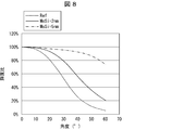
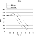
- a light emitting device ESB (indicated by “Ref” in FIG. 7) and a semitransparent metal layer 33, which are not provided with the translucent metal layer 33, are provided with MoSi having a layer thickness of 2 nm or 5 nm. It is a graph which shows the angle dependence of a light emitting element ESB. Further, FIG. 8 shows MoSi having a layer thickness of 2 nm or 5 nm as the comparative light emitting element ESG (indicated by “Ref” in FIG. 7) and the semitransparent metal layer 33, which are not provided with the semitransparent metal layer 33. It is a graph which shows the angle dependence of the provided light emitting element ESG. In FIG.
- the light emitting device ESR (indicated by “Ref” in FIG. 7) and the semitransparent metal layer 33, which are not provided with the translucent metal layer 33, are provided with MoSi having a layer thickness of 2 nm or 5 nm. It is a graph which shows the angle dependence of a light emitting element ESR. Further, Table 5 shows the reduction rate (front luminance ratio) of the front luminance in each light emitting element ESR / ESG / ESB, taking into consideration the absorption rate in the translucent metal layer 33.
- the angle dependence indicates the relationship between the angle and the brightness ratio to the front luminance when the front is 0 ° and the front luminance of the light emitting element indicated by Ref is 100%.
- the front luminance ratio shown in Table 5 indicates the front luminance of each light emitting element when the front luminance of the light emitting element shown by Ref is 100%.
- the front luminance, the front luminance ratio, and the angle dependence were compared by trial calculation of the emission luminance for each emission direction using the "SETFOS" manufactured by Cybernet.
- the same layer as the layer configuration used in the trial calculation (simulation) of the reflectance from the reflective metal layer 32 shown in FIGS. 4 to 6 is performed. The configuration was used.
- the semitransparent metal layer 33 by providing the semitransparent metal layer 33, a decrease in brightness in the oblique direction is suppressed as compared with the case where the semitransparent metal layer 33 is not provided. It turns out that it can be done. For example, when each light emitting element ESR / ESG / ESB is viewed from an oblique direction of 30 ° to 60 °, the brightness is reduced to about half or 10% of the front brightness when the semitransparent metal layer 33 is not provided. On the other hand, when the translucent metal layer 33 is provided, it is possible to obtain 5 to 50% higher brightness than when the semitransparent metal layer 33 is not provided.
- the light that is colored when viewed from an oblique direction is downward light (that is, light toward the first electrode 22 side), and the transmitted light and the reflected light interfere with each other, resulting in a difference in the optical path length when viewed from an oblique direction.
- interference fringes are generated and coloring occurs.
- the translucent metal layer 33 can absorb the downward light, reduce the interference effect due to the external light, and suppress the occurrence of interference fringes. Therefore, as described above, the viewing angle characteristic can be improved and the directivity can be lowered (light is emitted in all directions).
- the layer thickness of the translucent metal layer 33 is preferably in the range of 1 to 5 nm, and more preferably in the range of 2 nm or more and less than 5 nm. It is desirable, especially 2 nm.
- FIG. 10 is a cross-sectional view showing a schematic configuration of each light emitting element ESR, ESG, and ESB in the light emitting element layer 5 of the display device 1 according to the present embodiment.
- a second transparent electrode 34 is provided between the reflective metal layer 32 and the translucent metal layer 33. It is the same as the display device 1 according to the first embodiment except that the display device 1 is used.
- the first electrode 22 in each light emitting element ES has the first transparent electrode 31, the reflective metal layer 32, and the translucent metal layer from the lower layer side (that is, the thin film transistor layer 4 side). 33 and the second transparent electrode 34 are provided in this order.
- the translucent metal layer 33 such as MoSi has a large work function, and holes can be efficiently injected into the functional layer 24.
- the translucent metal layer 33 may be provided with at least one layer between the reflective metal layer 32 and the functional layer 24, and although not shown, the translucent metal layer 33 is a reflective metal as shown in FIG. It may be provided between the layer 32 and the second transparent electrode 34, and between the second transparent electrode 34 and the functional layer 24 as shown in FIG. That is, the translucent metal layer 33 includes the first translucent metal layer and the second translucent metal layer, and the first electrode 22 in each light emitting element ES is the first from the lower layer side (that is, the thin film layer 4 side). 1
- the transparent electrode 31, the reflective metal layer 32, the first translucent metal layer, the second transparent electrode 34, and the second translucent metal layer may be provided in this order.
- each light emitting element ESR / ESG / ESB is translucent.
- the thickness of the metal layer 33 may be changed.
- Display device 2 Support 4 Thin film transistor layer 5 Light emitting element layer 6 Sealing layer 22 1st electrode 24 Functional layer 25 2nd electrode 31 1st transparent electrode 34 2nd transparent electrode 32 Reflective metal layer 33 Semi-transparent metal layer 43R, 43G , 43B light emitting layer ESR / ESG / ESB light emitting element Tr thin film transistor
Landscapes
- Physics & Mathematics (AREA)
- Optics & Photonics (AREA)
- General Physics & Mathematics (AREA)
- Engineering & Computer Science (AREA)
- Theoretical Computer Science (AREA)
- Electroluminescent Light Sources (AREA)
Abstract
La présente invention concerne un dispositif d'affichage qui comprend une couche d'éléments électroluminescents qui a une pluralité d'éléments électroluminescents (ESR • ESG • ESB) pour lesquels une première électrode (22), une couche fonctionnelle (24) comprenant des couches électroluminescentes (43R • 43G • 43B), et une seconde électrode (25) étant disposées dans l'ordre indiqué à partir d'un côté couche de transistor en couches minces. La première électrode (22) comprend une première électrode transparente (31), une couche métallique réfléchissante (32), et une couche métallique translucide (33) dans l'ordre indiqué depuis le côté opposé à une couche électroluminescente (43).
Priority Applications (2)
| Application Number | Priority Date | Filing Date | Title |
|---|---|---|---|
| US17/440,757 US12120909B2 (en) | 2019-03-29 | 2019-03-29 | Display device |
| PCT/JP2019/014098 WO2020202284A1 (fr) | 2019-03-29 | 2019-03-29 | Dispositif d'affichage |
Applications Claiming Priority (1)
| Application Number | Priority Date | Filing Date | Title |
|---|---|---|---|
| PCT/JP2019/014098 WO2020202284A1 (fr) | 2019-03-29 | 2019-03-29 | Dispositif d'affichage |
Publications (1)
| Publication Number | Publication Date |
|---|---|
| WO2020202284A1 true WO2020202284A1 (fr) | 2020-10-08 |
Family
ID=72666623
Family Applications (1)
| Application Number | Title | Priority Date | Filing Date |
|---|---|---|---|
| PCT/JP2019/014098 Ceased WO2020202284A1 (fr) | 2019-03-29 | 2019-03-29 | Dispositif d'affichage |
Country Status (2)
| Country | Link |
|---|---|
| US (1) | US12120909B2 (fr) |
| WO (1) | WO2020202284A1 (fr) |
Cited By (1)
| Publication number | Priority date | Publication date | Assignee | Title |
|---|---|---|---|---|
| US20220328571A1 (en) * | 2021-04-08 | 2022-10-13 | Semiconductor Energy Laboratory Co., Ltd. | Display apparatus and electronic device |
Families Citing this family (1)
| Publication number | Priority date | Publication date | Assignee | Title |
|---|---|---|---|---|
| KR102931641B1 (ko) * | 2019-12-24 | 2026-02-26 | 오티아이 루미오닉스 인크. | 캡핑 층을 포함하는 발광 장치 및 그 제조방법 |
Citations (5)
| Publication number | Priority date | Publication date | Assignee | Title |
|---|---|---|---|---|
| JP2009295538A (ja) * | 2008-06-09 | 2009-12-17 | Sony Corp | 表示装置の製造方法および表示装置 |
| JP2010061951A (ja) * | 2008-09-03 | 2010-03-18 | Casio Comput Co Ltd | エレクトロルミネッセンスパネル及びエレクトロルミネッセンスパネルの製造方法 |
| JP2013157278A (ja) * | 2012-01-31 | 2013-08-15 | Canon Inc | 発光装置、画像形成装置及び撮像装置 |
| JP2018170126A (ja) * | 2017-03-29 | 2018-11-01 | ジオマテック株式会社 | 有機エレクトロルミネッセンス素子用電極、有機エレクトロルミネッセンス素子、有機エレクトロルミネッセンス表示装置、及び有機エレクトロルミネッセンス素子用電極の製造方法 |
| US20180375057A1 (en) * | 2017-06-26 | 2018-12-27 | Samsung Display Co., Ltd. | Light-emitting device and method of fabricating display panel therewith |
Family Cites Families (7)
| Publication number | Priority date | Publication date | Assignee | Title |
|---|---|---|---|---|
| JP4283551B2 (ja) | 2003-01-24 | 2009-06-24 | 日東電工株式会社 | 楕円偏光板および画像表示装置 |
| WO2008029060A2 (fr) * | 2006-09-07 | 2008-03-13 | Saint-Gobain Glass France | Substrat pour dispositif electroluminescent organique, utilisation et procede de fabrication de ce substrat, ainsi que dispositif electroluminescent organique. |
| JP5975831B2 (ja) * | 2011-10-31 | 2016-08-23 | キヤノン株式会社 | 表示装置 |
| JP6174877B2 (ja) * | 2013-03-21 | 2017-08-02 | 株式会社半導体エネルギー研究所 | 表示装置及び電子機器 |
| US9627445B2 (en) * | 2013-12-05 | 2017-04-18 | Infineon Technologies Dresden Gmbh | Optoelectronic component and a method for manufacturing an optoelectronic component |
| WO2015125581A1 (fr) * | 2014-02-24 | 2015-08-27 | コニカミノルタ株式会社 | Élément électroluminescent organique |
| WO2017056635A1 (fr) * | 2015-09-30 | 2017-04-06 | コニカミノルタ株式会社 | Élément électroluminescent organique |
-
2019
- 2019-03-29 WO PCT/JP2019/014098 patent/WO2020202284A1/fr not_active Ceased
- 2019-03-29 US US17/440,757 patent/US12120909B2/en active Active
Patent Citations (5)
| Publication number | Priority date | Publication date | Assignee | Title |
|---|---|---|---|---|
| JP2009295538A (ja) * | 2008-06-09 | 2009-12-17 | Sony Corp | 表示装置の製造方法および表示装置 |
| JP2010061951A (ja) * | 2008-09-03 | 2010-03-18 | Casio Comput Co Ltd | エレクトロルミネッセンスパネル及びエレクトロルミネッセンスパネルの製造方法 |
| JP2013157278A (ja) * | 2012-01-31 | 2013-08-15 | Canon Inc | 発光装置、画像形成装置及び撮像装置 |
| JP2018170126A (ja) * | 2017-03-29 | 2018-11-01 | ジオマテック株式会社 | 有機エレクトロルミネッセンス素子用電極、有機エレクトロルミネッセンス素子、有機エレクトロルミネッセンス表示装置、及び有機エレクトロルミネッセンス素子用電極の製造方法 |
| US20180375057A1 (en) * | 2017-06-26 | 2018-12-27 | Samsung Display Co., Ltd. | Light-emitting device and method of fabricating display panel therewith |
Cited By (2)
| Publication number | Priority date | Publication date | Assignee | Title |
|---|---|---|---|---|
| US20220328571A1 (en) * | 2021-04-08 | 2022-10-13 | Semiconductor Energy Laboratory Co., Ltd. | Display apparatus and electronic device |
| US12245485B2 (en) * | 2021-04-08 | 2025-03-04 | Semiconductor Energy Laboratory Co., Ltd. | Display apparatus including light-emitting device and light-receiving device |
Also Published As
| Publication number | Publication date |
|---|---|
| US12120909B2 (en) | 2024-10-15 |
| US20220181591A1 (en) | 2022-06-09 |
Similar Documents
| Publication | Publication Date | Title |
|---|---|---|
| US10916589B2 (en) | Electroluminescent display device | |
| US11251230B2 (en) | Organic EL display device | |
| KR101116825B1 (ko) | 유기전계발광표시장치 | |
| JP5425242B2 (ja) | 有機el素子及びこれを用いた表示装置 | |
| US9343510B2 (en) | Organic light emitting display device | |
| US20100283385A1 (en) | Organic el device | |
| TWI699022B (zh) | 發光裝置、顯示設備以及照明設備 | |
| US10217969B2 (en) | Organic light emitting diode display and method for fabricating the same | |
| WO2006054137A1 (fr) | Dispositif emetteur de lumiere organique comprenant des couches dielectriques de recouvrement | |
| JP5109303B2 (ja) | 有機発光素子および表示装置 | |
| CN110611037A (zh) | 显示装置及其制造方法 | |
| KR20120111798A (ko) | 유기전계 발광소자 | |
| JP2007005173A (ja) | 表示装置 | |
| KR102604263B1 (ko) | 표시장치 | |
| KR100683737B1 (ko) | 전계발광 디스플레이 장치 | |
| WO2020202284A1 (fr) | Dispositif d'affichage | |
| KR102113609B1 (ko) | 유기 발광 표시 장치 및 그의 제조 방법 | |
| WO2022168312A1 (fr) | Élément électroluminescent et dispositif d'affichage | |
| US7545096B2 (en) | Trans-reflective organic electroluminescent panel and method of fabricating the same | |
| CN114695782B (zh) | 发光显示装置 | |
| KR102231631B1 (ko) | 유기 발광 표시 장치 | |
| JP2004281189A (ja) | 上面発光型有機エレクトロルミネセンス表示素子およびその製造方法 | |
| US12310168B2 (en) | Display device | |
| KR101878326B1 (ko) | 유기전계 발광소자 | |
| KR20150137204A (ko) | 유기전계발광소자 |
Legal Events
| Date | Code | Title | Description |
|---|---|---|---|
| 121 | Ep: the epo has been informed by wipo that ep was designated in this application |
Ref document number: 19923232 Country of ref document: EP Kind code of ref document: A1 |
|
| NENP | Non-entry into the national phase |
Ref country code: DE |
|
| 122 | Ep: pct application non-entry in european phase |
Ref document number: 19923232 Country of ref document: EP Kind code of ref document: A1 |
|
| NENP | Non-entry into the national phase |
Ref country code: JP |