WO2020202954A1 - Structure de montage de composant électronique et procédé de fabrication associé - Google Patents
Structure de montage de composant électronique et procédé de fabrication associé Download PDFInfo
- Publication number
- WO2020202954A1 WO2020202954A1 PCT/JP2020/008342 JP2020008342W WO2020202954A1 WO 2020202954 A1 WO2020202954 A1 WO 2020202954A1 JP 2020008342 W JP2020008342 W JP 2020008342W WO 2020202954 A1 WO2020202954 A1 WO 2020202954A1
- Authority
- WO
- WIPO (PCT)
- Prior art keywords
- hole
- terminal
- electronic component
- circuit board
- connecting member
- Prior art date
- Legal status (The legal status is an assumption and is not a legal conclusion. Google has not performed a legal analysis and makes no representation as to the accuracy of the status listed.)
- Ceased
Links
Images



Classifications
-
- H—ELECTRICITY
- H05—ELECTRIC TECHNIQUES NOT OTHERWISE PROVIDED FOR
- H05K—PRINTED CIRCUITS; CASINGS OR CONSTRUCTIONAL DETAILS OF ELECTRIC APPARATUS; MANUFACTURE OF ASSEMBLAGES OF ELECTRICAL COMPONENTS
- H05K1/00—Printed circuits
- H05K1/02—Details
-
- H—ELECTRICITY
- H05—ELECTRIC TECHNIQUES NOT OTHERWISE PROVIDED FOR
- H05K—PRINTED CIRCUITS; CASINGS OR CONSTRUCTIONAL DETAILS OF ELECTRIC APPARATUS; MANUFACTURE OF ASSEMBLAGES OF ELECTRICAL COMPONENTS
- H05K1/00—Printed circuits
- H05K1/18—Printed circuits structurally associated with non-printed electric components
-
- H—ELECTRICITY
- H05—ELECTRIC TECHNIQUES NOT OTHERWISE PROVIDED FOR
- H05K—PRINTED CIRCUITS; CASINGS OR CONSTRUCTIONAL DETAILS OF ELECTRIC APPARATUS; MANUFACTURE OF ASSEMBLAGES OF ELECTRICAL COMPONENTS
- H05K3/00—Apparatus or processes for manufacturing printed circuits
- H05K3/30—Assembling printed circuits with electric components, e.g. with resistors
- H05K3/32—Assembling printed circuits with electric components, e.g. with resistors electrically connecting electric components or wires to printed circuits
- H05K3/34—Assembling printed circuits with electric components, e.g. with resistors electrically connecting electric components or wires to printed circuits by soldering
-
- H—ELECTRICITY
- H05—ELECTRIC TECHNIQUES NOT OTHERWISE PROVIDED FOR
- H05K—PRINTED CIRCUITS; CASINGS OR CONSTRUCTIONAL DETAILS OF ELECTRIC APPARATUS; MANUFACTURE OF ASSEMBLAGES OF ELECTRICAL COMPONENTS
- H05K7/00—Constructional details common to different types of electric apparatus
- H05K7/20—Modifications to facilitate cooling, ventilating, or heating
Definitions
- the present disclosure relates to an electronic component mounting structure and a method for manufacturing an electronic component mounting structure.
- This application claims the priority based on Japanese Patent Application No. 2019-070185 of the Japanese application dated April 1, 2019, and incorporates all the contents described in the Japanese application.
- the electronic unit shown in Patent Document 1 includes a circuit board, electronic components such as a power inductor mounted on the front surface of the circuit board, and a heat radiating member provided on the back surface of the circuit board.
- the mounting structure of the electronic component is A circuit board having a front surface and a back surface, With electronic components It is provided with a heat radiating member arranged on the back surface of the circuit board.
- the circuit board Through holes opened in the front surface and the back surface, It has a first through hole and a second through hole provided around the through hole.
- the electronic component is The main body housed in the through hole and It has a first terminal and a second terminal provided on the surface side of the circuit board in the main body.
- Each of the first through hole and the back surface side of the circuit board in the second through hole is thermally connected to the heat radiating member.
- Each of the first through hole and the surface side of the circuit board in the second through hole is thermally connected to each of the first terminal and the second terminal.
- the method for manufacturing the mounting structure of the electronic component according to the present disclosure is as follows.
- a main body having a first surface and a second surface facing the first surface, an electronic component having a first terminal and a second terminal provided on the second surface side of the main body, a first connecting member and a second connection.
- the main body portion penetrates the circuit board so that the first surface of the main body portion faces the back surface side of the circuit board and the second surface of the main body portion faces the front surface side of the circuit board.
- the process of storing in the hole and A step of electrically connecting each of the first terminal and the second terminal to each of the first connecting member and the second connecting member.
- the step includes a step of thermally connecting the heat radiating member facing the back surface of the circuit board and each of the back surface side of the circuit board in the first through hole and the second through hole.
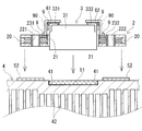
- FIG. 1 is a partial cross-sectional view showing an outline of a mounting structure of an electronic component according to the first embodiment.
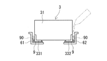
- FIG. 2A is an explanatory diagram illustrating step c in an example of a method for manufacturing a mounting structure of an electronic component according to the first embodiment.
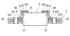
- FIG. 2B is an explanatory diagram illustrating step b in an example of a method for manufacturing a mounting structure of an electronic component according to the first embodiment.
- FIG. 2C is an explanatory diagram illustrating step e in an example of a method for manufacturing a mounting structure of an electronic component according to the first embodiment.
- FIG. 3 is an explanatory diagram illustrating step f in another example of the method of manufacturing the mounting structure of the electronic component according to the first embodiment.
- FIG. 1 is a partial cross-sectional view showing an outline of a mounting structure of an electronic component according to the first embodiment.
- FIG. 2A is an explanatory diagram illustrating step c in an example of a method for manufacturing a mounting structure of an electronic component according
- FIG. 4 is a partial cross-sectional view showing an outline of the mounting structure of the electronic component according to the first modification.
- FIG. 5 is a partial cross-sectional view showing an outline of the mounting structure of the electronic component according to the modified example 2.
- FIG. 6 is a partial cross-sectional view showing an outline of the mounting structure of the electronic component according to the modified example 3.
- one of the purposes of the present disclosure is to provide a mounting structure for an electronic component, which has a low protrusion height from the surface of the circuit board in the electronic component and has excellent heat dissipation of the electronic component.
- the present disclosure is different from providing a method for manufacturing an electronic component mounting structure capable of manufacturing an electronic component mounting structure having a low protrusion height from the surface of a circuit board in an electronic component and having excellent heat dissipation of the electronic component. It is one of the purposes of.
- the mounting structure of the electronic component according to the present disclosure has a low protrusion height from the surface of the circuit board in the electronic component, and is excellent in heat dissipation of the electronic component.
- the mounting structure of the electronic component is A circuit board having a front surface and a back surface, With electronic components It is provided with a heat radiating member arranged on the back surface of the circuit board.
- the circuit board Through holes opened in the front surface and the back surface, It has a first through hole and a second through hole provided around the through hole.
- the electronic component is The main body housed in the through hole and It has a first terminal and a second terminal provided on the surface side of the circuit board in the main body.
- Each of the first through hole and the back surface side of the circuit board in the second through hole is thermally connected to the heat radiating member.
- Each of the first through hole and the surface side of the circuit board in the second through hole is thermally connected to each of the first terminal and the second terminal.
- the above configuration has a low protrusion height from the surface of the circuit board in the electronic component, and is excellent in heat dissipation of the electronic component.
- the reason why the protruding height of the electronic component can be lowered is that the circuit board has a penetrating hole in which the main body of the electronic component can be housed.
- the reason why the heat dissipation of the electronic component is excellent is that the heat of the electronic component is transferred to the heat dissipation member from each of the first terminal and the second terminal of the electronic component through each of the first through hole and the second through hole of the circuit board. This is because the heat of the electronic component is transferred to the heat radiating member through the main body portion housed in the through hole.
- a first connecting member and a second connecting member that thermally connect each of the first terminal and the second terminal to each of the first through hole and the surface side of the circuit board in the second through hole.
- Have and Each of the first connecting member and the second connecting member may be composed of a member separate from each of the first terminal and the second terminal.
- first connecting member and a second connecting member which are composed of separate members from each of the first terminal and the second terminal, each of the first terminal and the second terminal of the electronic component and the first through It is easy to connect each of the hole and the second through hole.
- the heat radiating member may have a recess into which the main body is fitted.
- the first heat transfer member makes it easy to transfer the heat of the electronic component from the main body to the heat dissipation member.
- the second heat transfer member makes it easy to transfer the heat of the electronic component from each of the first through hole and the second through hole to the heat radiation member via each of the first terminal and the second terminal.
- An example includes a sealing resin portion that covers the surface of the electronic component and brings the electronic component into close contact with the circuit board.
- the thermal connection between the terminal of the electronic component and the through hole of the circuit board is hard to disconnect.
- the sealing resin portion can improve the adhesion between the electronic component and the circuit board.
- the method for manufacturing an electronic component mounting structure is as follows.
- a main body having a first surface and a second surface facing the first surface, an electronic component having a first terminal and a second terminal provided on the second surface side of the main body, a first connecting member and a second connection.
- the main body portion penetrates the circuit board so that the first surface of the main body portion faces the back surface side of the circuit board and the second surface of the main body portion faces the front surface side of the circuit board.
- the process of storing in the hole and A step of electrically connecting each of the first terminal and the second terminal to each of the first connecting member and the second connecting member.
- the step includes a step of thermally connecting the heat radiating member facing the back surface of the circuit board and each of the back surface side of the circuit board in the first through hole and the second through hole.
- the step of electrically connecting each of the first terminal and the second terminal to each of the first connecting member and the second connecting member may be performed before the step of accommodating the main body portion. ..
- the first terminal is between the step of electrically connecting each of the first terminal and the second terminal and each of the first connecting member and the second connecting member and the step of accommodating the main body portion.
- a step of fixing each of the second terminals and each of the first connecting member and the second connecting member with an adhesive can be mentioned.
- the above configuration can reinforce the connection between the electronic component and the first connecting member and the second connecting member. Therefore, when the assembly connecting the electronic component and the first connecting member and the second connecting member is housed in the through hole of the substrate, the connection between the electronic component and the first connecting member and the second connecting member is disconnected. hard.
- a step of electrically connecting each of the first terminal and the second terminal to each of the first connecting member and the second connecting member, and each of the first connecting member and the second connecting member and the first may be performed by reflow soldering after the step of accommodating the main body portion.
- the mounting structure 1 of the electronic component of the first embodiment will be described with reference to FIG.
- the electronic component mounting structure 1 of the present embodiment includes a circuit board 2 having a front surface and a back surface, an electronic component 3, and a heat radiating member 4 arranged on the back surface of the circuit board 2.
- the front surface and the back surface of the circuit board 2 face each other.
- One of the features of the electronic component mounting structure 1 in this embodiment is that the circuit board 2 and the electronic component 3 satisfy the following configurations, respectively.
- the circuit board 2 has a through hole 21 and a first through hole 221 and a second through hole 222 that are thermally connected to the heat radiating member 4.
- the electronic component 3 is upside down and has a main body 31 housed in the through hole 21 and a first terminal 331 and a second terminal 332 provided on the surface side of the circuit board 2 in the main body 31.
- Each of the first terminal 331 and the second terminal 332 is thermally connected to each of the surface sides of the circuit board 2 in the first through hole 221 and the second through hole 222.
- the back surface side of the circuit board 2 is the bottom side
- the front surface side is the top side.
- the back surface side is the lower side of the paper surface
- the front surface side is the upper side of the paper surface.
- the length of the circuit board 2, the electronic component 3, the heat radiating member 4, the first heat transfer member 51 described later, and the second heat transfer member 52 described later in the vertical direction of FIG. 1 may be referred to as a thickness.
- these thicknesses are schematically shown for convenience of explanation, and do not necessarily correspond to actual thicknesses.
- the circuit board 2 is typically a plate-shaped member that constitutes a predetermined circuit such as a signal circuit, a part of a power circuit, and a current or voltage detection circuit (FIG. 1).
- a printed circuit board (PCB) can be used as the circuit board 2.
- the circuit board 2 is composed of a double-sided board in which circuit patterns are provided on the front and back sides of the insulating board 20.
- the circuit board 2 may be composed of a single-sided substrate in which a circuit pattern is provided on one of the front and back surfaces of the insulating substrate 20, or a multilayer substrate in which the insulating substrate 20 and the circuit pattern are stacked.
- the circuit pattern is made of copper foil.
- This circuit pattern has a first land 231 and a second land 232.
- each of the first terminal 331 and the second terminal 332 of the electronic component 3 is electrically and mechanically connected.
- the circuit board 2 has a through hole 21, a first through hole 221 and a second through hole 222.
- the through hole 21 is a hole for accommodating the main body 31 of the electronic component 3 described later. Through the through hole 21, the mounting structure 1 of the electronic component can reduce the protruding height of the electronic component 3 from the upper surface of the circuit board 2.
- the through holes 21 are opened on the upper surface and the lower surface of the circuit board 2.
- the size of the through hole 21 when the through hole 21 is viewed in a plan view is not particularly limited as long as it can accommodate the main body 31.
- the plan view means viewing from the axial direction of the through hole 21.
- the size of the through hole 21 is one size larger than that of the main body 31 in this embodiment.
- the planar shape of the through hole 21 may be similar to the planar shape of the main body 31.
- the planar shape refers to a shape in which the through hole 21 is viewed from above and below.
- the planar shape of the through hole 21 is rectangular in this embodiment.
- a conductor layer is not provided on the inner peripheral surface of the through hole 21.
- Each of the first through hole 221 and the second through hole 222 thermally connects each of the first terminal 331 and the second terminal 332 of the electronic component 3 to the heat radiating member 4.
- the first through hole 221 and the second through hole 222 are through hole vias.
- This thermal connection refers to a connection state in which a heat dissipation path can be formed from each of the first terminal 331 and the second terminal 332 to the heat radiating member 4 via each of the first through hole 221 and the second through hole 222.
- the members of the first terminal 331, the first through hole 221 and the heat radiating member 4 are in direct contact with each other, or a solid or viscous body is interposed between at least a part of the members. is there.
- each member of the second terminal 332, the second through hole 222, and the heat radiating member 4 is in direct contact with each other, or a solid or viscous body is interposed between at least a part of each member. ..
- each member constituting the heat dissipation path is higher than the thermal conductivity of the insulating substrate 20. That is, although the detailed heat dissipation path will be described later, the first terminal 331, the second terminal 332, the solder 9, the first connecting member 61, the second connecting member 62, the first land 231 and the second land 232, the first through hole 221 It is preferable that all the constituent materials of the second through hole 222 and the second heat transfer member 52 are higher than the thermal conductivity of the insulating substrate 20. The same meaning applies to thermal connections between other members.
- This heat dissipation path has a larger amount of heat dissipation than other places excluding the heat dissipation path from the main body 31 to the recess 41, which will be described later.
- each of the first through hole 221 and the second through hole 222 transfers the heat of the electronic component 3 to the heat radiating member 4 via each of the first terminal 331 and the second terminal 332.
- the first through hole 221 and the second through hole 222 may form a part of the above-mentioned circuit.
- the first through hole 221 and the second through hole 222 are formed around the through hole 21.
- a plurality of first through holes 221 are provided on the first terminal 331 side of the electronic component 3 in the through hole 21, and a plurality of second through holes 222 are provided on the second terminal 332 side of the electronic component 3 in the through hole 21.
- FIG. 1 shows one first through hole 221 with an exaggerated size on the first terminal 331 side of the through hole 21, and one exaggerated size on the second terminal 332 side of the through hole 21.
- the second through hole 222 is shown.
- the first through hole 221 and the second through hole 222 have a through hole opened on the upper surface and the lower surface of the circuit board 2 and a conductor layer provided on the inner peripheral surface of the through hole.
- the conductor layer is preferably made of metal.
- the conductor layer of this embodiment is made of copper.
- Each of the first through hole 221 and the second through hole 222 is electrically and mechanically connected to each of the first land 231 and the second land 232 on the upper surface side.
- each of the first connecting member 61 and the second connecting member 62 which will be described later, are electrically and mechanically connected to each of the first land 231 and the second land 232 on the upper surface side.
- Each of the first connecting member 61 and the second connecting member 62 is electrically and mechanically connected to each of the first terminal 331 and the second terminal 332 of the electronic component 3. That is, each of the first through hole 221 and the second through hole 222 and each of the first terminal 331 and the second terminal 332 are indirectly connected. By this indirect connection, each of the first through hole 221 and the second through hole 222 and each of the first terminal 331 and the second terminal 332 are thermally connected.
- Each of the lower surface side of the circuit board 2 in the first through hole 221 and the second through hole 222 is mechanically in contact with the second heat transfer member 52 described later in this embodiment.
- the heat radiating member 4 is mechanically in contact with the second heat transfer member 52. That is, each of the first through hole 221 and the second through hole 222 and the heat radiating member 4 are indirectly connected. By this indirect connection, each of the first through hole 221 and the second through hole 222 and the heat radiating member 4 are thermally connected.
- Each of the first through hole 221 and the second through hole 222 on the lower surface side of the circuit board 2 may be in mechanical contact with the heat radiating member 4 without passing through the second heat transfer member 52.
- each of the first through hole 221 and the second through hole 222 is directly connected to the heat radiating member 4.
- each of the first through hole 221 and the second through hole 222 and the heat radiating member 4 are thermally connected. Therefore, each of the first terminal 331 and the second terminal 332 and the heat radiating member 4 are thermally connected via each of the first through hole 221 and the second through hole 222.
- the electronic component 3 is mounted on the upper surface of the circuit board 2.
- the electronic component 3 has a main body 31, a first terminal 331, and a second terminal 332.
- the electronic component 3 is a power inductor in this embodiment.
- Other types of electronic components 3 include inductors, transformers, semiconductor elements, resistors, capacitors, and the like.
- a power inductor usually has a core, a coil, and first and second terminals.
- the core is made of soft magnetic material. This core corresponds to the main body 31 in this embodiment.
- the coil is embedded in the core.
- Each of the first and second terminals of the power inductor is connected to each of the first and second ends of the coil.
- Each of the first and second terminals of the power inductor is exposed from the core.
- Each of the first terminal and the second terminal of the power inductor corresponds to each of the first terminal 331 and the second terminal 332 in this embodiment.
- the core is composed of a powder compact formed by compression molding soft magnetic powder.
- the particles constituting the soft magnetic powder include soft magnetic metal particles, coated particles having an insulating coating on the outer periphery of the soft magnetic metal particles, and soft magnetic non-metal particles.
- the soft magnetic metal include pure iron and iron-based alloys.
- the iron-based alloy include Fe—Si alloys and Fe—Ni alloys.
- the insulating coating include phosphate and the like.
- Examples of the soft magnetic non-metal include ferrite and the like.
- the coil has a winding portion and a first end portion and a second end portion.
- the winding portion is formed by spirally winding the winding, and the winding can be a covered wire having an insulating coating on the outer circumference of the conductor wire.
- Examples of the material of the conductor wire include metals such as copper and copper alloys.
- Examples of the type of conductor wire include a round wire.
- Examples of the insulating coating include enamel. Typical examples of enamel include polyamide-imide.
- the winding may be composed of a coated round wire.
- the shape of the winding portion may be cylindrical.
- the axis of the winding portion is along the vertical direction in this embodiment. That is, the shaft of the winding portion is along the axial direction of the through hole 21.
- Each of the first terminal 331 and the second terminal 332 is connected to each of the first end portion and the second end portion.
- the shape of the main body 31 is not particularly limited and can be appropriately selected.
- the shape of the main body 31 is a rectangular parallelepiped in this embodiment.
- the lower surface of the main body 31 is in mechanical contact with the first heat transfer member 51, which will be described later in this embodiment.
- the first heat transfer member 51 is in mechanical contact with the recess 41 of the heat dissipation member 4, which will be described later. That is, the main body 31 and the recess 41 are indirectly connected. By this indirect connection, the main body 31 and the recess 41 are thermally connected.
- the lower surface of the main body 31 may be in direct contact with the heat radiating member 4, that is, the recess 41 in this embodiment, without passing through the first heat transfer member 51. In that case, the main body 31 is directly connected to the recess 41. By this direct connection, the main body 31 and the recess 41 are thermally connected.
- Each of the first terminal 331 and the second terminal 332 is thermally connected to each of the first through hole 221 and the second through hole 222.
- the connection of the first terminal 331 and the second terminal 332 to each of the first through hole 221 and the second through hole 222 is connected to each of the first land 231 and the second land 232 in this embodiment. This is performed via each of the first connecting member 61 and the second connecting member 62, which will be described later. That is, each of the first terminal 331 and the second terminal 332 and each of the first through hole 221 and the second through hole 222 are indirectly connected. By this indirect connection, each of the first terminal 331 and the second terminal 332 and each of the first through hole 221 and the second through hole 222 are thermally connected.
- each of the first terminal 331 and the second terminal 332 does not go through each of the first connecting member 61 and the second connecting member 62, but the first land 231 And each of the second land 232 may be electrically and mechanically connected.
- each of the first terminal 331 and the second terminal 332 is directly connected to each of the first land 231 and the second land 232.
- each of the first terminal 331 and the second terminal 332 and each of the first through hole 221 and the second through hole 222 are thermally connected.
- each of the first terminal 331 and the second terminal 332 and each of the first through hole 221 and the second through hole 222 are indirectly connected.
- each of the first terminal 331 and the second terminal 332 and each of the first through hole 221 and the second through hole 222 are thermally connected.
- the method of connecting via each of the first connecting member 61 and the second connecting member 62 will be described later.
- the first terminal 331 and the second terminal 332 are made of a plate material made of a conductive material.
- the conductive material include metals such as copper and copper alloys.
- the first terminal 331 and the second terminal 332 are bent so as to be provided from the side surface to the upper surface of the main body portion 31.
- the upper surfaces of the first terminal 331 and the second terminal 332 project upward from the upper surface of the main body 31 by substantially the thickness of each of the first terminal 331 and the second terminal 332.
- Each side surface of the first terminal 331 and the second terminal 332 is substantially flush with the side surface of the main body 31.
- Each of the first connecting member 61 and the second connecting member 62 thermally connects each of the first terminal 331 and the second terminal 332 to each of the first through hole 221 and the second through hole 222. Due to this thermal connection, each of the first connecting member 61 and the second connecting member 62 transfers the heat of the electronic component 3 through the first terminal 331 and the second terminal 332 through the first through hole 221 and the second through hole 221 and the second. It is transmitted to each of the through holes 222.
- the first connecting member 61 and the second connecting member 62 are composed of members separate from each of the first terminal 331 and the second terminal 332. One end of each of the first connecting member 61 and the second connecting member 62 is electrically and mechanically connected to each of the first terminal 331 and the second terminal 332. The other ends of each of the first connecting member 61 and the second connecting member 62 are electrically and mechanically connected to each of the first land 231 and the second land 232 on the upper surface side. Since the first connecting member 61 and the second connecting member 62 are formed of separate members from each of the first terminal 331 and the second terminal 332, each of the first connecting member 61 and the second connecting member 62 is the first. It is easy to connect each of the terminals 331 and the second terminal 332 to each of the first land 231 and the second land 232.
- first connecting member 61 and the second connecting member 62 For the connection of one end and the other end of each of the first connecting member 61 and the second connecting member 62, a connecting material made of metal can be used. As this metal, solder 9 can be typically used. In the middle of each of the first connecting member 61 and the second connecting member 62, one end and the other end thereof are equal to the thickness between the upper surfaces of the first terminal 331 and the second terminal 332 and the upper surface of the circuit board 2. It is bent in an S shape so that a step is formed.
- the first connecting member 61 and the second connecting member 62 are plate materials made of a conductive material. Examples of the conductive material include the same materials as those of the first terminal 331 and the second terminal 332.
- the heat radiating member 4 releases heat from the circuit board 2 and the electronic component 3.
- the material of the heat radiating member 4 include a material having excellent thermal conductivity. As such a material, for example, a metal such as aluminum or an aluminum alloy is suitable.
- the heat radiating member 4 is arranged on the lower surface of the circuit board 2. Although the heat radiating member 4 has the recess 41 in this embodiment, the heat radiating member 4 may not have the recess 41.
- the recess 41 is thermally connected to the main body 31. This thermal connection refers to a connection state in which a heat dissipation path from the main body 31 to the recess 41 can be configured.
- the members of the main body 31 and the recess 41 are in direct contact with each other, or a solid or viscous body is interposed between at least a part of the members.
- This heat dissipation path is compared with other places excluding the heat dissipation path from each of the first terminal 331 and the second terminal 332 described above to the heat dissipation member 4 via each of the first through hole 221 and the second through hole 222. The amount of heat dissipation is large.
- the main body 31 is fitted in the recess 41.
- the recess 41 is provided so that a region of the heat radiating member 4 facing the main body 31 is locally recessed.
- the planar shape of the recess 41 may be similar to the planar shape of the main body 31.
- the planar shape of the recess 41 is rectangular.
- the depth of the recess 41 is not particularly limited and can be appropriately selected.
- the depth of the recess 41 may be, for example, such that the sum of the depth of the recess 41 and the thickness of the circuit board 2 is equal to or greater than the thickness of the main body 31.
- the upper surface of the main body 31 may be flush with the upper surface of the circuit board 2, or may be located below the upper surface of the circuit board 2. Therefore, the protruding height of the electronic component 3 can be substantially eliminated.
- the heat radiating member 4 has fins 42 described later as in the present embodiment, the deeper the depth of the recess 41, the more the heat dissipation performance of the region where the recess 41 is provided becomes the peripheral region of the recess 41 excluding the recess 41. It may be lower than the heat dissipation performance.
- a protruding portion is formed in the region corresponding to the lower part of the concave portion 41 by the depth of the concave portion 41 so as to protrude downward from the lower surface of the peripheral region.
- the fin 42 corresponding to the lower part of the recess 41 extends downward from the lower surface of the protrusion.
- the fin 42 corresponding to the lower side of the peripheral region extends downward from the lower surface of the peripheral region.
- the length of the fin 42 corresponding to the lower part of the recess 41 is shortened by the depth of the recess 41, that is, by the protrusion height of the protrusion. Since this protrusion serves as a flow resistance for the fluid flowing between the fins 42 and the length of the fins 42 is short, the heat dissipation performance of the region where the recess 41 is provided is improved around the recess 41 excluding the recess 41. It is lower than the heat dissipation performance of the area. Therefore, the depth of the recess 41 may be appropriately selected so that the upper surface of the main body 31 projects upward from the upper surface of the circuit board 2.
- the heat radiating member 4 preferably further includes fins 42.
- the fin 42 tends to increase the surface area of the heat radiating member 4 to improve the heat radiating property.
- the fin 42 is composed of a plurality of protrusions protruding downward from the lower surface of the heat radiating member 4.
- the second heat transfer member 52 easily transfers the heat of the electronic component 3 from each of the first through hole 221 and the second through hole 222 to the heat radiating member 4 via each of the first terminal 331 and the second terminal 332.
- the second heat transfer member 52 is provided over substantially the entire area between the lower surface of the circuit board 2 and the peripheral region of the recess 41 excluding the recess 41 in the heat dissipation member 4.
- the first heat transfer member 51 and the second heat transfer member 52 may be formed independently of each other as in the present embodiment, or may be formed in a series.
- the first heat transfer member 51 and the second heat transfer member 52 are preferably made of a material having a higher thermal conductivity than the insulating substrate 20.
- Both the first heat transfer member 51 and the second heat transfer member 52 may be formed of a heat radiating grease or a heat radiating sheet, or may be made of an insulating sheet having excellent heat radiating properties.
- the thermal paste include silicone grease.
- the heat radiating sheet include a silicone gel sheet. It is preferable that the heat radiating grease and the heat radiating sheet contain a filler. Specific examples of the filler include alumina filler. Thermal paste and heat dissipation sheet are relatively soft.
- the thermal paste and the heat dissipation sheet are connected to the first land 231 and the second land 232 of the first terminal 331 and the second terminal 332 by the solder 9 without being disconnected, and the lower surface and the recess of the main body 31 are not disconnected. It is easy to fill the gap with the upper surface of 41.
- the insulating sheet having excellent heat dissipation include a thermosetting resin such as a silicone resin or an epoxy resin containing the above-mentioned filler.
- the mounting structure 1 of the electronic component may further include an insulating member.
- the insulating member is interposed between the recess 41 and the first heat transfer member 51, or between the peripheral region of the recess 41 in the heat dissipation member 4 and the second heat transfer member 52.
- the insulating member can enhance the electrical insulation between the electronic component 3 and the circuit board 2 and the heat radiating member 4.
- Examples of the insulating member include an insulating sheet made of the above-mentioned thermosetting resin.
- the mounting structure 1 of the electronic component may further include a sealing resin portion 7.
- the sealing resin portion 7 covers the surface of the electronic component 3 and brings the electronic component 3 and the circuit board 2 into close contact with each other.
- the covering region of the sealing resin portion 7 may be a region that covers the outside of the first connecting member 61 and the second connecting member 62. If the first connecting member 61 and the second connecting member 62 are also covered with the sealing resin portion 7, each of the first terminal 331 and the second terminal 332 and the circuit board by each of the first connecting member 61 and the second connecting member 62 are covered. It is easy to maintain the connection with 2.
- the sealing resin portion 7 is provided from the first through hole 221 to the second through hole 222 so as to straddle the electronic component 3. Examples of the material of the sealing resin portion 7 include a thermoplastic resin similar to the insulating sheet.
- the mounting structure 1 of the electronic component of this embodiment has a low protruding height of the electronic component 3, and is excellent in heat dissipation of the electronic component 3.
- the reason why the protruding height of the electronic component 3 can be lowered is that the circuit board 2 has a through hole 21 capable of accommodating the main body 31 of the electronic component 3.
- the reason why the electronic component 3 is excellent in heat dissipation is that the heat of the electronic component 3 is transferred to the first terminal 331 and the second terminal of the electronic component 3 through each of the first through hole 221 and the second through hole 222 of the circuit board 2. This is because the heat of the electronic component 3 is transferred to the heat radiating member 4 through the main body 31 housed in the through hole 21 in addition to being transferred to the heat radiating member 4 from each of the 332s.
- the method for manufacturing the mounting structure of the electronic component in the present embodiment includes the following steps a to e.
- the electronic component mounting structure 1 is manufactured by the method for manufacturing the electronic component mounting structure.
- the order of steps b to e can be appropriately selected from the following steps b.
- Typical examples of the method for manufacturing the mounting structure of the electronic component in this embodiment include the following manufacturing method I and manufacturing method II.
- step a a circuit board, an electronic component, a first connecting member, a second connecting member, and a heat radiating member are prepared.
- step b the main body of the electronic component is housed in the through hole of the circuit board. This storage is performed so that the first surface of the main body faces the back surface side of the circuit board and the second surface of the main body faces the front surface side of the circuit board.
- step c each of the first terminal and the second terminal of the electronic component and each of the first connecting member and the second connecting member are electrically connected.
- step d each of the first connecting member and the second connecting member is thermally connected to each of the first through hole of the circuit board and each of the surface side of the circuit board in the second through hole.
- step e the heat radiating member facing the back surface of the circuit board and each of the back surface sides of the circuit board in the first through hole and the second through hole are thermally connected.
- the manufacturing method I will be described with reference to FIGS. 2A to 2C.
- the manufacturing method I goes through each step in the order of step a, step c, step b, step d, and step e.
- step a the circuit board 2, the electronic component 3, the first connecting member 61, the second connecting member 62, and the heat radiating member 4 are prepared (FIGS. 2A to 2C).
- the circuit board 2 has a through hole 21, a first through hole 221 and a second through hole 222, and a first land 231 and a second land 232.
- the through hole 21 opens on the front surface and the back surface of the insulating substrate 20.
- the front surface is the upper side of the paper surface and the back surface is the lower side of the paper surface.
- the first through hole 221 and the second through hole 222 are provided around the through hole 21.
- the electronic component 3 has a main body portion 31 and a first terminal 331 and a second terminal 332.
- the main body 31 has a first surface and a second surface facing the first surface.
- the first surface is the upper side of the paper surface
- the second surface is the lower side of the paper surface of FIG. 2A.
- the first terminal 331 and the second terminal 332 are provided on the second surface side of the main body 31.
- the first connecting member 61 and the second connecting member 62 are made of a plate material bent in an S shape.
- the heat radiating member 4 has a recess 41 provided on the upper surface and fins 42 provided on the lower surface.
- step c In step c, as shown in FIG. 2A, each of the first terminal 331 and the second terminal 332 of the electronic component 3 and each of the first connecting member 61 and the second connecting member 62 are electrically connected. Solder 9 can be used for this electrical connection.
- the connection with the solder 9 can be performed by the reflow method.
- the connection by soldering 9 may be performed by hand soldering.
- a braid in which and is integrated is produced.
- the electronic component 3 and each of the first connecting member 61 and the second connecting member 62 can be handled as one member in the step b, so that the step b and the subsequent step d can be handled. Easy to work.
- each of the first terminal 331 and the second terminal 332 and each of the first connecting member 61 and the second connecting member 62 may be further fixed by the adhesive 90.
- the solder 9 can firmly connect each of the first terminal 331 and the second terminal 332 to each of the first connecting member 61 and the second connecting member 62. Further, if each of the first terminal 331 and the second terminal 332 and each of the first connecting member 61 and the second connecting member 62 are fixed with the adhesive 90, each of the first terminal 331 and the second terminal 332 and the first Each of the connecting member 61 and the second connecting member 62 can be fixed more firmly.
- the adhesive 90 may be filled between each of the first terminal 331 and the second terminal 332 and each of the first connecting member 61 and the second connecting member 62.
- the type of the adhesive 90 is not particularly limited and can be appropriately selected as long as the adhesive strength is maintained when the main body 31 is stored in the step b.
- a known heat-resistant adhesive can be preferably used as the type of the adhesive 90.
- step b the main body 31 is housed in the through hole 21 of the circuit board 2.
- the main body 31 is stored by turning the assembly upside down. That is, the first surface of the main body 31 faces the back surface side of the circuit board 2, and the second surface of the main body 31 faces the front surface side of the circuit board 2. Further, in the storage of the main body 31, each of the first connecting member 61 and the second connecting member 62 integrated with the electronic component 3 is soldered on each of the first land 231 and the second land 232 of the circuit board 2. Make contact with 9.
- each of the first connecting member 61 and the second connecting member 62 and each of the surface sides of the circuit board 2 in the first through hole 221 and the second through hole 222 are thermally connected. Connecting. This thermal connection is made up of the first connecting member 61 and each of the first land 231 and the second land 232 that are electrically and mechanically connected to each of the first through hole 221 and the second through hole 222. This can be done by electrically and mechanically connecting each of the second connecting members 62. As in the step c described above, the solder 9 can be used for this connection. The connection with the solder 9 can be performed by the reflow method. The connection by soldering 9 may be performed by hand soldering.
- step e the heat radiating member 4 is arranged on the back surface of the circuit board 2.
- the back surface side of the circuit board 2 in the first through hole 221 and the second through hole 222 and the heat radiating member 4 are thermally connected.
- the first heat transfer member 51 and the second heat transfer member 52 are provided on the upper surface of the recess 41 of the heat radiating member 4 and the upper surface of the peripheral region of the recess 41.
- the integrated object is arranged on the upper surface of the heat radiating member 4. This arrangement is performed so that the main body 31 fits into the recess 41.
- the production method II will be described mainly with reference to FIG.
- the manufacturing method II is different from the manufacturing method I in that the step f in which the steps c and d are performed together is performed after the step b. That is, the manufacturing method II goes through each step in the order of step a, step b, step f, and step e.
- the step a is the same as the manufacturing method I described above.
- Step b In step b, as shown in FIG. 3, the main body 31 is housed in the through hole 21 of the circuit board 2.
- the jig 100 positions the circuit board 2 and the electronic component 3.
- the jig 100 includes the distance between the inner peripheral surface of the through hole 21 and the main body 31, each of the first terminal 331 and the second terminal 332, and the first land 231 on the upper surface side of the circuit board 2. Match the height with each of the second land 232.
- the jig 100 has a recess 101 corresponding to the recess 41 of the heat radiating member 4.
- the circuit board 2 is arranged on the upper surface of the jig 100.
- This arrangement is performed so that the through hole 21 of the circuit board 2 and the recess 101 of the jig 100 communicate with each other.
- the vertically inverted main body 31 is housed in the through hole 21 and fitted into the recess 101.
- the arrangement of the circuit board 2 in the jig 100 and the storage of the main body 31 in the through hole 21 are in no particular order. That is, the vertically inverted main body 31 is arranged in the recess 101 of the jig 100.
- the circuit board 2 may be arranged on the upper surface of the jig 100 so that the main body 31 is inserted into the through hole 21.
- Step f is an electrical and mechanical operation of each of the first terminal 331 and the second terminal 332 of the electronic component 3 and one end of each of the first connecting member 61 and the second connecting member 62.
- solder paste is pre-printed on the surfaces of the first land 231 and the second land 232 of the circuit board 2 and the surfaces of the first terminal 331 and the second terminal 332 of the electronic component 3.
- Either the printing of the solder paste on the surfaces of the first land 231 and the second land 232 and the printing of the solder paste on the surfaces of the first terminal 331 and the second terminal 332 may be performed first. These prints may be performed after step b or before step b.
- one end and the other end of each of the first connecting member 61 and the second connecting member 62 are attached to the solder paste on the surfaces of the first terminal 331 and the second terminal 332, and the first land 231 and the second land 232. Contact with the solder paste on each surface of. Then, the solder paste is heated and cured.
- each of the first terminal 331 and the second terminal 332 is connected to each of the first connecting member 61 and the second connecting member 62, and each of the first connecting member 61 and the second connecting member 62.
- the connection with each of the first through hole 221 and the second through hole 222 can be performed collectively. Therefore, the manufacturing process can be simplified.
- an integral body in which the circuit board 2 and the electronic component 3 are connected by each of the first connecting member 61 and the second connecting member 62 can be manufactured.
- step e In step e, as described above with reference to FIG. 2C, the integrated object is arranged on the upper surface of the heat radiating member 4. With this arrangement, each of the back surface side of the circuit board 2 in the first through hole 221 and the second through hole 222 and the heat radiating member 4 are thermally connected.
- each step may be performed in any of the following orders (i) to (iii).
- Step a, step b, step e, step f (Ii) Step a, step e, step b, step f (Iii) Step a, step e, step c, step b, step d
- the step c and the step d may be performed individually. In that case, the steps c and d are in no particular order.
- the method for manufacturing the mounting structure of the electronic component in the present embodiment can manufacture the mounting structure 1 of the electronic component having a low protruding height of the electronic component 3 and excellent heat dissipation of the electronic component 3.
- the manufacturing method I since the electronic component 3 and each of the first connecting member 61 and the second connecting member 62 can be handled as one member, the manufacturing work can be easily performed as compared with the manufacturing method II.
- each of the first terminal 331 and the second terminal 332 is connected to each of the first connecting member 61 and the second connecting member 62, and each of the first connecting member 61 and the second connecting member 62 and the first Since the connection with each of the one through hole 221 and the second through hole 222 can be performed collectively, the manufacturing process can be simplified as compared with the manufacturing method I.
- FIG. 4 is a partial cross-sectional view showing an enlarged mounting structure of the electronic component of the modified example 1 at a position similar to the position surrounded by the broken line rectangular frame shown in FIG. This point is the same in FIGS. 5 and 6 referred to in the modified examples 2 and 3 described later.
- the mounting structure of the electronic component of this example is the same as the mounting structure of the electronic component of the first embodiment except for the structure of the electronic component 3. The description of the same configuration as that of the first embodiment in this example will be omitted. This point is the same in the modified example 2 and the modified example 3 described later.
- a power inductor in which the upper surfaces of the first terminal 331 and the second terminal and the upper surface of the main body 31 are substantially flush with each other can be manufactured as follows. First, the raw material powder is compression-molded in a state where the coil and a part of each of the first terminal 331 and the second terminal are embedded in the raw material powder of the core constituting the main body 31. This compression molding is performed so that a step corresponding to the thickness of each of the first terminal 331 and the second terminal is provided on the upper surface of the main body 31. Then, each of the first terminal 331 and the second terminal exposed from the core is press-molded along the stepped portion on the upper surface from the side surface of the core.
- ⁇ Modification 2 [Mounting structure of electronic components]
- the upper surfaces of the first terminal 331 and the second terminal of the electronic component 3 can be positioned below the upper surface of the main body 31.
- the positions of the upper surfaces of the first terminal 331 and the second terminal along the vertical direction are such that the upper surfaces of the first connecting member 61 and the second connecting member are substantially flush with the upper surface of the main body 31.
- the electronic component 3 of this example can be manufactured by the same manufacturing method as that of the modified example 1.
- Each of the first terminal 331 and the second terminal has a uniform thickness in this example. If each of the first terminal 331 and the second terminal can be connected to each of the first land 231 and the second land, the main body portion of the pieces constituting each of the first terminal 331 and the second terminal.
- the piece along the upper surface of the main body 31 may be thinner or thicker than the piece along the side surface of the main body 31.
- Each of the first terminal 331 and the second terminal protrudes from the side surface of the main body 31.
- each of the first terminal 331 and the second terminal can be connected without passing through the first connection member 61 and the second connection member 62 shown in FIG. It can be directly connected to each of the first land 231 and the second land.
- the protrusion amount of each of the first terminal 331 and the second terminal may be a length from the side surface of the main body 31 to reach each of the first land 231 and the second land.
- the amount of protrusion of each of the first terminal 331 and the second terminal exceeds the length from the side surface of the main body 31 to the edge on the through hole 21 side of each of the first land 231 and the second land, and the main body 31
- the length from the side surface to the edge of each side of the first through hole 221 and the second through hole in each of the first land 231 and the second land may be less than or equal to the length.
Landscapes
- Engineering & Computer Science (AREA)
- Microelectronics & Electronic Packaging (AREA)
- Physics & Mathematics (AREA)
- Thermal Sciences (AREA)
- Manufacturing & Machinery (AREA)
- Cooling Or The Like Of Semiconductors Or Solid State Devices (AREA)
Abstract
Structure de montage de composant électronique comprenant une carte de circuit imprimé ayant des surfaces avant et arrière ; un composant électronique ; et un élément de dissipation de chaleur disposé sur la surface arrière de la carte de circuit imprimé. La carte de circuit imprimé comprend une ouverture traversante qui est ouverte sur les surfaces avant et arrière, ainsi qu'un premier et un second trou traversant qui sont disposés autour de l'ouverture traversante. Le composant électronique comprend une partie corps logée dans l'ouverture traversante, ainsi qu'une première et une seconde borne avec lesquelles la partie corps est disposée sur le côté surface avant de la carte de circuit imprimé. Le premier et le second trou traversant sur le côté de surface arrière de la carte de circuit imprimé sont thermiquement connectés à l'élément de dissipation de chaleur. Le premier trou traversant et le second trou traversant sur le côté de surface avant de la carte de circuit imprimé sont connectés de manière thermique respectivement aux premier et second terminaux.
Applications Claiming Priority (2)
| Application Number | Priority Date | Filing Date | Title |
|---|---|---|---|
| JP2019070185 | 2019-04-01 | ||
| JP2019-070185 | 2019-04-01 |
Publications (1)
| Publication Number | Publication Date |
|---|---|
| WO2020202954A1 true WO2020202954A1 (fr) | 2020-10-08 |
Family
ID=72668563
Family Applications (1)
| Application Number | Title | Priority Date | Filing Date |
|---|---|---|---|
| PCT/JP2020/008342 Ceased WO2020202954A1 (fr) | 2019-04-01 | 2020-02-28 | Structure de montage de composant électronique et procédé de fabrication associé |
Country Status (1)
| Country | Link |
|---|---|
| WO (1) | WO2020202954A1 (fr) |
Cited By (1)
| Publication number | Priority date | Publication date | Assignee | Title |
|---|---|---|---|---|
| CN117177473A (zh) * | 2023-10-18 | 2023-12-05 | 芜湖雅葆轩电子科技股份有限公司 | 一种元件贴装前的罩式分区定点融锡装置 |
Citations (5)
| Publication number | Priority date | Publication date | Assignee | Title |
|---|---|---|---|---|
| JPH07231053A (ja) * | 1994-02-16 | 1995-08-29 | Oki Electric Ind Co Ltd | 発熱体の放熱構造 |
| JP2000174179A (ja) * | 1998-12-07 | 2000-06-23 | Pioneer Electronic Corp | 発熱素子の放熱構造 |
| JP2009123736A (ja) * | 2007-11-12 | 2009-06-04 | Nec Corp | デバイスの実装構造及びデバイスの実装方法 |
| JP2011066332A (ja) * | 2009-09-18 | 2011-03-31 | Hitachi Automotive Systems Ltd | 制御装置の放熱構造 |
| JP2015060923A (ja) * | 2013-09-18 | 2015-03-30 | Fdk株式会社 | 電子モジュール |
-
2020
- 2020-02-28 WO PCT/JP2020/008342 patent/WO2020202954A1/fr not_active Ceased
Patent Citations (5)
| Publication number | Priority date | Publication date | Assignee | Title |
|---|---|---|---|---|
| JPH07231053A (ja) * | 1994-02-16 | 1995-08-29 | Oki Electric Ind Co Ltd | 発熱体の放熱構造 |
| JP2000174179A (ja) * | 1998-12-07 | 2000-06-23 | Pioneer Electronic Corp | 発熱素子の放熱構造 |
| JP2009123736A (ja) * | 2007-11-12 | 2009-06-04 | Nec Corp | デバイスの実装構造及びデバイスの実装方法 |
| JP2011066332A (ja) * | 2009-09-18 | 2011-03-31 | Hitachi Automotive Systems Ltd | 制御装置の放熱構造 |
| JP2015060923A (ja) * | 2013-09-18 | 2015-03-30 | Fdk株式会社 | 電子モジュール |
Cited By (1)
| Publication number | Priority date | Publication date | Assignee | Title |
|---|---|---|---|---|
| CN117177473A (zh) * | 2023-10-18 | 2023-12-05 | 芜湖雅葆轩电子科技股份有限公司 | 一种元件贴装前的罩式分区定点融锡装置 |
Similar Documents
| Publication | Publication Date | Title |
|---|---|---|
| US10672555B2 (en) | Surface-mountable coil element | |
| CN1627457B (zh) | 磁性元件及磁性元件的制造方法 | |
| US7646589B2 (en) | Solid electrolytic capacitor with first and second anode wires | |
| JP2000331835A (ja) | 積層電子部品及び回路モジュール | |
| JP2011243870A (ja) | コイル実装基板 | |
| JP7404744B2 (ja) | コイル部品の製造方法 | |
| JP2008199720A (ja) | 電源モジュール | |
| TWI451455B (zh) | Inductor and its manufacturing method | |
| JP4946488B2 (ja) | 回路モジュール | |
| JP2009218531A (ja) | インダクタとその製造方法とこれを用いた回路モジュール | |
| WO2018193828A1 (fr) | Substrat équipé d'un élément métallique, structure de circuit et boîte de connexion électrique | |
| CN111064344A (zh) | 具有底部金属散热基板的功率模块 | |
| JP2012190955A (ja) | 射出成型基板 | |
| JP6447368B2 (ja) | コイル部品 | |
| JP5397012B2 (ja) | 部品内蔵配線板、部品内蔵配線板の製造方法 | |
| WO2020202954A1 (fr) | Structure de montage de composant électronique et procédé de fabrication associé | |
| JP6477262B2 (ja) | コイル部品 | |
| JP6520480B2 (ja) | コイル部品 | |
| JP2020088290A (ja) | インダクタンス素子及び電子機器 | |
| JP5369875B2 (ja) | 部品内蔵配線板、部品内蔵配線板の製造方法 | |
| CN215815865U (zh) | 一种半导体模块及封装结构 | |
| JP2004349400A (ja) | 熱伝導性回路基板およびそれを用いたパワーモジュール | |
| US20180332709A1 (en) | Inductor component and method of manufacturing inductor component | |
| JP6879355B2 (ja) | コイル部品の製造方法 | |
| WO2018074188A1 (fr) | Composant de bobine d'inductance et procédé de fabrication de composant de bobine d'inductance |
Legal Events
| Date | Code | Title | Description |
|---|---|---|---|
| 121 | Ep: the epo has been informed by wipo that ep was designated in this application |
Ref document number: 20782538 Country of ref document: EP Kind code of ref document: A1 |
|
| NENP | Non-entry into the national phase |
Ref country code: DE |
|
| 122 | Ep: pct application non-entry in european phase |
Ref document number: 20782538 Country of ref document: EP Kind code of ref document: A1 |
|
| NENP | Non-entry into the national phase |
Ref country code: JP |