WO2020208698A1 - Substrat lié et procédé permettant de fabriquer un substrat lié - Google Patents
Substrat lié et procédé permettant de fabriquer un substrat lié Download PDFInfo
- Publication number
- WO2020208698A1 WO2020208698A1 PCT/JP2019/015414 JP2019015414W WO2020208698A1 WO 2020208698 A1 WO2020208698 A1 WO 2020208698A1 JP 2019015414 W JP2019015414 W JP 2019015414W WO 2020208698 A1 WO2020208698 A1 WO 2020208698A1
- Authority
- WO
- WIPO (PCT)
- Prior art keywords
- copper plate
- silicon nitride
- main surface
- nitride ceramic
- bonded substrate
- Prior art date
- Legal status (The legal status is an assumption and is not a legal conclusion. Google has not performed a legal analysis and makes no representation as to the accuracy of the status listed.)
- Ceased
Links
Images






Classifications
-
- C—CHEMISTRY; METALLURGY
- C04—CEMENTS; CONCRETE; ARTIFICIAL STONE; CERAMICS; REFRACTORIES
- C04B—LIME, MAGNESIA; SLAG; CEMENTS; COMPOSITIONS THEREOF, e.g. MORTARS, CONCRETE OR LIKE BUILDING MATERIALS; ARTIFICIAL STONE; CERAMICS; REFRACTORIES; TREATMENT OF NATURAL STONE
- C04B37/00—Joining burned ceramic articles with other burned ceramic articles or other articles by heating
- C04B37/02—Joining burned ceramic articles with other burned ceramic articles or other articles by heating with metallic articles
- C04B37/023—Joining burned ceramic articles with other burned ceramic articles or other articles by heating with metallic articles characterised by the interlayer used
- C04B37/026—Joining burned ceramic articles with other burned ceramic articles or other articles by heating with metallic articles characterised by the interlayer used consisting of metals or metal salts
-
- H—ELECTRICITY
- H05—ELECTRIC TECHNIQUES NOT OTHERWISE PROVIDED FOR
- H05K—PRINTED CIRCUITS; CASINGS OR CONSTRUCTIONAL DETAILS OF ELECTRIC APPARATUS; MANUFACTURE OF ASSEMBLAGES OF ELECTRICAL COMPONENTS
- H05K3/00—Apparatus or processes for manufacturing printed circuits
- H05K3/02—Apparatus or processes for manufacturing printed circuits in which the conductive material is applied to the surface of the insulating support and is thereafter removed from such areas of the surface which are not intended for current conducting or shielding
- H05K3/06—Apparatus or processes for manufacturing printed circuits in which the conductive material is applied to the surface of the insulating support and is thereafter removed from such areas of the surface which are not intended for current conducting or shielding the conductive material being removed chemically or electrolytically, e.g. by photo-etch process
-
- H—ELECTRICITY
- H05—ELECTRIC TECHNIQUES NOT OTHERWISE PROVIDED FOR
- H05K—PRINTED CIRCUITS; CASINGS OR CONSTRUCTIONAL DETAILS OF ELECTRIC APPARATUS; MANUFACTURE OF ASSEMBLAGES OF ELECTRICAL COMPONENTS
- H05K3/00—Apparatus or processes for manufacturing printed circuits
- H05K3/38—Improvement of the adhesion between the insulating substrate and the metal
- H05K3/382—Improvement of the adhesion between the insulating substrate and the metal by special treatment of the metal
- H05K3/383—Improvement of the adhesion between the insulating substrate and the metal by special treatment of the metal by microetching
-
- H—ELECTRICITY
- H10—SEMICONDUCTOR DEVICES; ELECTRIC SOLID-STATE DEVICES NOT OTHERWISE PROVIDED FOR
- H10W—GENERIC PACKAGES, INTERCONNECTIONS, CONNECTORS OR OTHER CONSTRUCTIONAL DETAILS OF DEVICES COVERED BY CLASS H10
- H10W40/00—Arrangements for thermal protection or thermal control
- H10W40/20—Arrangements for cooling
- H10W40/25—Arrangements for cooling characterised by their materials
- H10W40/255—Arrangements for cooling characterised by their materials having a laminate or multilayered structure, e.g. direct bond copper [DBC] ceramic substrates
-
- H—ELECTRICITY
- H10—SEMICONDUCTOR DEVICES; ELECTRIC SOLID-STATE DEVICES NOT OTHERWISE PROVIDED FOR
- H10W—GENERIC PACKAGES, INTERCONNECTIONS, CONNECTORS OR OTHER CONSTRUCTIONAL DETAILS OF DEVICES COVERED BY CLASS H10
- H10W70/00—Package substrates; Interposers; Redistribution layers [RDL]
- H10W70/60—Insulating or insulated package substrates; Interposers; Redistribution layers
- H10W70/67—Insulating or insulated package substrates; Interposers; Redistribution layers characterised by their insulating layers or insulating parts
- H10W70/69—Insulating materials thereof
- H10W70/692—Ceramics or glasses
-
- C—CHEMISTRY; METALLURGY
- C04—CEMENTS; CONCRETE; ARTIFICIAL STONE; CERAMICS; REFRACTORIES
- C04B—LIME, MAGNESIA; SLAG; CEMENTS; COMPOSITIONS THEREOF, e.g. MORTARS, CONCRETE OR LIKE BUILDING MATERIALS; ARTIFICIAL STONE; CERAMICS; REFRACTORIES; TREATMENT OF NATURAL STONE
- C04B2237/00—Aspects relating to ceramic laminates or to joining of ceramic articles with other articles by heating
- C04B2237/02—Aspects relating to interlayers, e.g. used to join ceramic articles with other articles by heating
- C04B2237/12—Metallic interlayers
- C04B2237/122—Metallic interlayers based on refractory metals
-
- C—CHEMISTRY; METALLURGY
- C04—CEMENTS; CONCRETE; ARTIFICIAL STONE; CERAMICS; REFRACTORIES
- C04B—LIME, MAGNESIA; SLAG; CEMENTS; COMPOSITIONS THEREOF, e.g. MORTARS, CONCRETE OR LIKE BUILDING MATERIALS; ARTIFICIAL STONE; CERAMICS; REFRACTORIES; TREATMENT OF NATURAL STONE
- C04B2237/00—Aspects relating to ceramic laminates or to joining of ceramic articles with other articles by heating
- C04B2237/02—Aspects relating to interlayers, e.g. used to join ceramic articles with other articles by heating
- C04B2237/12—Metallic interlayers
- C04B2237/125—Metallic interlayers based on noble metals, e.g. silver
-
- C—CHEMISTRY; METALLURGY
- C04—CEMENTS; CONCRETE; ARTIFICIAL STONE; CERAMICS; REFRACTORIES
- C04B—LIME, MAGNESIA; SLAG; CEMENTS; COMPOSITIONS THEREOF, e.g. MORTARS, CONCRETE OR LIKE BUILDING MATERIALS; ARTIFICIAL STONE; CERAMICS; REFRACTORIES; TREATMENT OF NATURAL STONE
- C04B2237/00—Aspects relating to ceramic laminates or to joining of ceramic articles with other articles by heating
- C04B2237/30—Composition of layers of ceramic laminates or of ceramic or metallic articles to be joined by heating, e.g. Si substrates
- C04B2237/32—Ceramic
- C04B2237/36—Non-oxidic
- C04B2237/368—Silicon nitride
-
- C—CHEMISTRY; METALLURGY
- C04—CEMENTS; CONCRETE; ARTIFICIAL STONE; CERAMICS; REFRACTORIES
- C04B—LIME, MAGNESIA; SLAG; CEMENTS; COMPOSITIONS THEREOF, e.g. MORTARS, CONCRETE OR LIKE BUILDING MATERIALS; ARTIFICIAL STONE; CERAMICS; REFRACTORIES; TREATMENT OF NATURAL STONE
- C04B2237/00—Aspects relating to ceramic laminates or to joining of ceramic articles with other articles by heating
- C04B2237/30—Composition of layers of ceramic laminates or of ceramic or metallic articles to be joined by heating, e.g. Si substrates
- C04B2237/40—Metallic
- C04B2237/407—Copper
-
- C—CHEMISTRY; METALLURGY
- C04—CEMENTS; CONCRETE; ARTIFICIAL STONE; CERAMICS; REFRACTORIES
- C04B—LIME, MAGNESIA; SLAG; CEMENTS; COMPOSITIONS THEREOF, e.g. MORTARS, CONCRETE OR LIKE BUILDING MATERIALS; ARTIFICIAL STONE; CERAMICS; REFRACTORIES; TREATMENT OF NATURAL STONE
- C04B2237/00—Aspects relating to ceramic laminates or to joining of ceramic articles with other articles by heating
- C04B2237/50—Processing aspects relating to ceramic laminates or to the joining of ceramic articles with other articles by heating
- C04B2237/52—Pre-treatment of the joining surfaces, e.g. cleaning, machining
-
- C—CHEMISTRY; METALLURGY
- C04—CEMENTS; CONCRETE; ARTIFICIAL STONE; CERAMICS; REFRACTORIES
- C04B—LIME, MAGNESIA; SLAG; CEMENTS; COMPOSITIONS THEREOF, e.g. MORTARS, CONCRETE OR LIKE BUILDING MATERIALS; ARTIFICIAL STONE; CERAMICS; REFRACTORIES; TREATMENT OF NATURAL STONE
- C04B2237/00—Aspects relating to ceramic laminates or to joining of ceramic articles with other articles by heating
- C04B2237/50—Processing aspects relating to ceramic laminates or to the joining of ceramic articles with other articles by heating
- C04B2237/55—Pre-treatments of a coated or not coated substrate other than oxidation treatment in order to form an active joining layer
-
- C—CHEMISTRY; METALLURGY
- C04—CEMENTS; CONCRETE; ARTIFICIAL STONE; CERAMICS; REFRACTORIES
- C04B—LIME, MAGNESIA; SLAG; CEMENTS; COMPOSITIONS THEREOF, e.g. MORTARS, CONCRETE OR LIKE BUILDING MATERIALS; ARTIFICIAL STONE; CERAMICS; REFRACTORIES; TREATMENT OF NATURAL STONE
- C04B2237/00—Aspects relating to ceramic laminates or to joining of ceramic articles with other articles by heating
- C04B2237/50—Processing aspects relating to ceramic laminates or to the joining of ceramic articles with other articles by heating
- C04B2237/70—Forming laminates or joined articles comprising layers of a specific, unusual thickness
-
- C—CHEMISTRY; METALLURGY
- C04—CEMENTS; CONCRETE; ARTIFICIAL STONE; CERAMICS; REFRACTORIES
- C04B—LIME, MAGNESIA; SLAG; CEMENTS; COMPOSITIONS THEREOF, e.g. MORTARS, CONCRETE OR LIKE BUILDING MATERIALS; ARTIFICIAL STONE; CERAMICS; REFRACTORIES; TREATMENT OF NATURAL STONE
- C04B2237/00—Aspects relating to ceramic laminates or to joining of ceramic articles with other articles by heating
- C04B2237/50—Processing aspects relating to ceramic laminates or to the joining of ceramic articles with other articles by heating
- C04B2237/86—Joining of two substrates at their largest surfaces, one surface being complete joined and covered, the other surface not, e.g. a small plate joined at it's largest surface on top of a larger plate
-
- C—CHEMISTRY; METALLURGY
- C04—CEMENTS; CONCRETE; ARTIFICIAL STONE; CERAMICS; REFRACTORIES
- C04B—LIME, MAGNESIA; SLAG; CEMENTS; COMPOSITIONS THEREOF, e.g. MORTARS, CONCRETE OR LIKE BUILDING MATERIALS; ARTIFICIAL STONE; CERAMICS; REFRACTORIES; TREATMENT OF NATURAL STONE
- C04B2237/00—Aspects relating to ceramic laminates or to joining of ceramic articles with other articles by heating
- C04B2237/50—Processing aspects relating to ceramic laminates or to the joining of ceramic articles with other articles by heating
- C04B2237/88—Joining of two substrates, where a substantial part of the joining material is present outside of the joint, leading to an outside joining of the joint
-
- H—ELECTRICITY
- H05—ELECTRIC TECHNIQUES NOT OTHERWISE PROVIDED FOR
- H05K—PRINTED CIRCUITS; CASINGS OR CONSTRUCTIONAL DETAILS OF ELECTRIC APPARATUS; MANUFACTURE OF ASSEMBLAGES OF ELECTRICAL COMPONENTS
- H05K1/00—Printed circuits
- H05K1/02—Details
- H05K1/03—Use of materials for the substrate
- H05K1/0306—Inorganic insulating substrates, e.g. ceramic, glass
-
- H—ELECTRICITY
- H05—ELECTRIC TECHNIQUES NOT OTHERWISE PROVIDED FOR
- H05K—PRINTED CIRCUITS; CASINGS OR CONSTRUCTIONAL DETAILS OF ELECTRIC APPARATUS; MANUFACTURE OF ASSEMBLAGES OF ELECTRICAL COMPONENTS
- H05K2203/00—Indexing scheme relating to apparatus or processes for manufacturing printed circuits covered by H05K3/00
- H05K2203/14—Related to the order of processing steps
- H05K2203/1476—Same or similar kind of process performed in phases, e.g. coarse patterning followed by fine patterning
-
- H—ELECTRICITY
- H05—ELECTRIC TECHNIQUES NOT OTHERWISE PROVIDED FOR
- H05K—PRINTED CIRCUITS; CASINGS OR CONSTRUCTIONAL DETAILS OF ELECTRIC APPARATUS; MANUFACTURE OF ASSEMBLAGES OF ELECTRICAL COMPONENTS
- H05K3/00—Apparatus or processes for manufacturing printed circuits
- H05K3/38—Improvement of the adhesion between the insulating substrate and the metal
Definitions
- the present invention relates to a bonded substrate and a method for manufacturing the bonded substrate.
- Silicon nitride ceramics have high thermal conductivity and high insulation. Therefore, a bonded substrate in which a copper plate is bonded to a silicon nitride ceramic substrate via a bonding layer is suitably used as an insulating heat-dissipating substrate on which a power semiconductor element is mounted.
- the bonded substrate is produced by producing an intermediate product in which the brazing material layer is between the copper plate and the silicon nitride ceramic substrate, and the produced intermediate product is heat-treated to change the brazing material layer into a bonded layer, and the copper plate is used. And manufactured by patterning the bonding layer.
- the copper circuit board is joined to at least one surface of the ceramic substrate formed of silicon nitride via a brazing material layer (paragraphs 0013 and 0020).
- the ceramic circuit board has a brazing material protruding portion protruding outward from the side surface of the copper circuit board (paragraph 0013).
- the thermal stress is relieved, so that a highly reliable ceramic-metal junction circuit board can be realized (paragraph 0013).
- the thermal cycle durability of the bonded substrate is improved by forming a protruding portion protruding from between the silicon nitride ceramic substrate and the copper plate. ing.
- the protruding portion cannot be formed, it is expected to improve the thermal cycle durability of the bonded substrate. Further, even when the protruding portion can be formed, it is expected that the thermal cycle durability of the bonded substrate is further improved.
- An object to be solved by the present invention is to improve the thermal cycle durability of a bonded substrate in which a copper plate is bonded to a silicon nitride ceramic substrate via a bonding layer.
- the present invention is directed to a bonded substrate.
- the bonding substrate includes a silicon nitride ceramic substrate, a bonding layer, and a copper plate.
- the bonding layer and the copper plate are arranged on the silicon nitride ceramic substrate.
- the second main surface of the copper plate is on the side opposite to the side where the first main surface of the copper plate is located, and is bonded to the silicon nitride ceramic substrate by the bonding layer.
- the end faces of the copper plate extend from the first main surface of the copper plate to the second main surface of the copper plate.
- the end face of the copper plate has a first part and a second part.
- the second part is closer to the second main surface than the first part.
- the first part and the second part form an angle of 135 ° or more and 165 ° or less outside the copper plate.
- the distance from the second main surface to the intersection of the first portion and the second portion in the thickness direction of the copper plate is 10 ⁇ m or more and 100 ⁇ m or less.
- the distance extending beyond the extension surface of the first portion of the second main surface is 10 ⁇ m or more.
- the present invention is also directed to a method for manufacturing a bonded substrate.
- a brazing material layer is formed on the silicon nitride ceramic substrate.
- the brazing filler metal layer contains an active metal brazing filler metal.
- the active metal brazing material includes a metal powder containing silver and at least one hydrogenated metal powder selected from the group consisting of titanium hydride powder and zirconium hydride powder.
- a copper plate is placed on the brazing material layer.
- an intermediate product including a silicon nitride ceramic substrate, a brazing material layer and a copper plate can be obtained.
- the brazing material layer changes into a bonding layer that joins the copper plate to the silicon nitride ceramic substrate.
- silver contained in the brazing material layer diffuses into the copper plate.
- the copper plate is formed with a first thickness direction region containing silver and having a first silver concentration, and a second thickness direction region having a second silver concentration lower than the first silver concentration.
- first thickness direction region is etched at the first etching rate
- second thickness direction region is etched at the second etching rate faster than the first etching rate
- FIG. 5 is an enlarged cross-sectional view schematically showing a part of the bonded substrate of the first embodiment.
- FIG. 5 is an enlarged cross-sectional view schematically showing a part of the bonded substrate of the first embodiment.
- It is a flowchart which shows the manufacturing flow of the bonded substrate of 1st Embodiment.
- It is sectional drawing which shows typically the intermediate product obtained in the process of manufacturing the bonded substrate of 1st Embodiment.
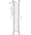
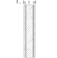
- FIG. 1 is a cross-sectional view schematically showing the bonded substrate of the first embodiment.
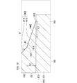
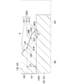
- 2 and 3 are enlarged cross-sectional views schematically showing a part of the bonded substrate of the first embodiment. 2 and 3 show a part A of FIG. 1 in an enlarged manner.
- the bonding substrate 100 of the first embodiment includes a silicon nitride ceramic substrate 110, a bonding layer 121, a copper plate 131, a bonding layer 122, and a copper plate 132.
- the bonded substrate 100 may include elements other than these elements.
- One set of the joining layer 121 and the copper plate 131, and one set of the joining layer 122 and the copper plate 132 may be omitted.
- the bonding layer 121 and the copper plate 131 are arranged on the main surface 1101 of the silicon nitride ceramic substrate 110.
- the bonding layer 122 and the copper plate 132 are arranged on the main surface 1102 of the silicon nitride ceramic substrate 110.
- the copper plates 131 and 132 are bonded to the silicon nitride ceramic substrate 110 by the bonding layers 121 and 122, respectively.
- the copper plates 131 and 132 are brazed to the main surfaces 1101 and 1102 of the silicon nitride ceramic substrate 110 by the active metal brazing method by the bonding layers 121 and 122, respectively.
- the bonded substrate 100 may be used in any way, and is used, for example, as an insulated heat-dissipating substrate on which a power semiconductor element is mounted.
- each of the copper plates contained in the copper plates 131 and 132 is referred to as a copper plate 130
- the bonding layer included in the bonding layers 121 and 122 for bonding the copper plate 130 to the silicon nitride ceramic substrate 110 is referred to as a bonding layer 120.
- the copper plate 130 has a first main surface 1301, a second main surface 1302, and an end surface 1303, as shown in FIG.
- the second main surface 1302 is on the side opposite to the side where the first main surface 1301 is located, and is bonded to the silicon nitride ceramic substrate 110 by the bonding layer 120.
- the end face 1303 extends from the first main surface 1301 to the second main surface 1302.
- the end face 1303 has a bump 1400 illustrated in FIG. 2 or FIG.
- the end face 1303 has the bump 1400 shown in FIG. 2, the end face 1303 has a first portion 1411 and a second portion 1412.
- the second portion 1412 is closer to the second main surface 1302 than the first portion 1411.
- Each of the first portion 1411 and the second portion 1412 is substantially flat.
- the first portion 1411 and the second portion 1412 form an angle ⁇ 1 of 135 ° or more and 165 ° or less outside the copper plate 130.
- the intersection 1421 of the first portion 1411 and the second portion 1412 is preferably separated from the second main surface 1302 by a distance L1 of 10 ⁇ m or more and 100 ⁇ m or less in the thickness direction of the copper plate 130, and more preferably. It is separated from the second main surface 1302 by a distance L1 of 10 ⁇ m or more and 60 ⁇ m or less in the thickness direction of the copper plate 130.
- the second main surface 1302 extends beyond the extension surface 1414 of the first portion 1411 by a distance L2 of 10 ⁇ m or more.
- the extension surface 1414 has the same normal direction as the normal direction of the first portion 1411 at the position closest to the second main surface 1302 of the first portion 1411.
- the copper plate 130 has an angle 1421 formed by the first portion 1411 and the second portion 1412, and an angle 1423 formed by the second main surface 1302 and the end surface 1303.
- the bonded substrate 100 is exposed to a thermal cycle, it is dispersed in the vicinity of the corners 1421 and 1423 to generate stress. Therefore, the stress generated in the vicinity of each of the angles 1421 and 1423 becomes small. As a result, the thermal cycle durability of the bonded substrate 100 is improved.
- the angle ⁇ 1 When the angle ⁇ 1 is smaller than 135 °, the stress is concentrated too much in the vicinity of the angle 1421, and it tends to be difficult to obtain the effect of improving the thermal cycle durability of the bonded substrate 100.
- the angle ⁇ 1 When the angle ⁇ 1 is larger than 165 °, the stress is not dispersed in the vicinity of the angle 1421, and it tends to be difficult to obtain the effect of improving the thermal cycle durability of the bonded substrate 100.
- the distance L1 is 10 ⁇ m or more and 100 ⁇ m or less, the cold cycle durability of the bonded substrate 100 can be further improved, and when the distance L1 is 10 ⁇ m or more and 60 ⁇ m or less, the cold cycle durability of the bonded substrate 100 is particularly improved. Can be improved.
- the distance L1 When the distance L1 is shorter than these ranges, the angles 1421 and 1423 approach each other, the stress is not dispersed, and it tends to be difficult to obtain the effect of improving the thermal cycle durability of the bonded substrate 100.
- the distance L1 When the distance L1 is longer than these ranges, stress does not occur in the vicinity of the corner 1421, and it tends to be difficult to obtain the effect of improving the thermal cycle durability of the bonded substrate 100.
- the distance L2 When the distance L2 is shorter than 10 ⁇ m, the stress is not dispersed, and it tends to be difficult to obtain the effect of improving the thermal cycle durability of the bonded substrate 100.
- the end face 1303 has the bump 1400 shown in FIG. 3, the end face 1303 has a first portion 1411, a second portion 1412, and a third portion 1413.
- the second portion 1412 is closer to the second main surface 1302 than the first portion 1411.
- the third portion 1413 is closer to the second main surface 1302 than the second portion 1412.
- Each of the first portion 1411, the second portion 1412 and the third portion 1413 is substantially flat.
- the first portion 1411 and the second portion 1412 form an angle ⁇ 1 of 135 ° or more and 165 ° or less outside the copper plate 130.
- the second portion 1412 and the third portion 1413 form an angle ⁇ 2 of 135 ° or more and 165 ° or less inside the copper plate 130.
- the intersection 1421 of the first portion 1411 and the second portion 1412 is preferably separated from the second main surface 1302 by a distance L1 of 10 ⁇ m or more and 100 ⁇ m or less in the thickness direction of the copper plate 130, and more preferably. It is separated from the second main surface 1302 by a distance L1 of 10 ⁇ m or more and 60 ⁇ m or less in the thickness direction of the copper plate 130.
- the second main surface 1302 extends beyond the extension surface 1414 of the first portion 1411 by a distance L2 of 10 ⁇ m or more.
- the extension surface 1414 has the same normal direction as the normal direction of the first portion 1411 at the position closest to the second main surface 1302 of the first portion 1411.
- the copper plate 130 has an angle 1421 formed by the first portion 1411 and the second portion 1412, an angle 1422 formed by the second portion 1412 and the third portion 1413, and a second main surface 1302 and an end surface 1303. It has an angle of 1423.
- the bonded substrate 100 is exposed to a thermal cycle, it is dispersed in the vicinity of angles 1421, 1422 and 1423 to generate stress. Therefore, the stress generated in the vicinity of each of the angles 1421, 1422 and 1423 becomes small. As a result, the thermal cycle durability of the bonded substrate 100 is improved.
- the thermal cycle durability of the bonded substrate 100 is further improved as compared with the case where the stress is dispersed only in the corners 1421 and 1423.
- the angle ⁇ 1 When the angle ⁇ 1 is smaller than 135 °, the stress is concentrated too much in the vicinity of the angle 1421, and it tends to be difficult to obtain the effect of improving the thermal cycle durability of the bonded substrate 100. When the angle ⁇ 1 is larger than 165 °, the stress is not dispersed in the vicinity of the angle 1421, and it tends to be difficult to obtain the effect of improving the thermal cycle durability of the bonded substrate 100. The same can be said for the angle ⁇ 2. When the distance L1 is 10 ⁇ m or more and 100 ⁇ m or less, the cold cycle durability of the bonded substrate 100 can be further improved, and when the distance L1 is 10 ⁇ m or more and 60 ⁇ m or less, the cold cycle durability of the bonded substrate 100 is particularly improved. Can be improved.
- the distance L1 When the distance L1 is shorter than these ranges, the angles 1421, 1422 and 1423 approach each other, the stress is not dispersed in a wide range, and it becomes difficult to obtain the effect of improving the thermal cycle durability of the bonded substrate 100. A tendency appears.
- the distance L1 is longer than these ranges, the stress is not dispersed in the vicinity of the corners 1421 and 1422, and it tends to be difficult to obtain the effect of improving the thermal cycle durability of the bonded substrate 100.
- the distance L2 When the distance L2 is shorter than 10 ⁇ m, the stress is not dispersed, and it tends to be difficult to obtain the effect of improving the thermal cycle durability of the bonded substrate 100.
- the copper plate 130 has a distribution of silver concentration in which the silver concentration decreases as the distance from the second main surface 1302 increases.
- the copper plate 130 includes a first thickness-direction region 151 containing silver and having a first silver concentration, and a second silver having a silver concentration lower than that of the first silver. It has a second thickness direction region 152 having a concentration.
- the fact that the second thickness region 152 has a second silver concentration lower than the first silver concentration means that the second thickness region 152 does not contain silver, and the second thickness region 152 Includes silver but the second silver concentration is less than the first silver concentration, but the former is desirable.
- the first thickness direction region 151 has a second portion 1412. If the end face 1303 has the bump 1400 shown in FIG. 3, the first thickness region 151 has a second portion 1412 and a third portion 1413.
- the second thickness direction region 152 has a first portion 1411.
- the first thickness direction region 151 has a first etching rate with respect to the etching solution for the copper plate 130.
- the second thickness direction region 152 has a second etching rate with respect to the etching solution.
- the second etching rate is faster than the first etching rate.
- the second etching rate is faster than the first etching rate because the second silver concentration is lower than the first silver concentration.
- the bump 1400 on the end face 1303 is formed by etching by utilizing the fact that the second etching rate is faster than the first etching rate.
- the bump 1400 of the end face 1303 may be formed by other than etching.
- the bump 1400 on the end face 1303 may be formed by machining.
- the bonding layer 120 includes an inter-plate portion 160 and a protruding portion 161 as shown in FIGS. 1, 2 and 3.
- the inter-plate portion 160 is located between the silicon nitride ceramic substrate 110 and the copper plate 130.
- the protruding portion 161 protrudes from between the silicon nitride ceramic substrate 110 and the copper plate 130.
- the concentration of stress on the end portion of the copper plate 130 is relaxed by the protruding portion 161. As a result, it is possible to suppress defects in the bonded substrate 100 due to stress concentration on the ends of the copper plate 130.
- the bonding layer 120 preferably has a thickness of 0.1 ⁇ m or more and 5 ⁇ m or less, and more preferably 0.1 ⁇ m or more and 3 ⁇ m or less. Since the bonding layer 120 has such a small thickness, the concentration of stress on the end portion of the copper plate 130 is effectively alleviated by the protruding portion 161.
- the copper plate 130 preferably has a thickness of 0.5 mm or more.
- a bonded substrate 100 having high heat dissipation can be obtained.
- the copper plate 130 has a thickness of 0.5 mm or more, a large stress is generated in the copper plate 130, and the thermal cycle durability of the bonded substrate 100 tends to decrease.
- the above-mentioned effect of improving the cooling cycle durability of the bonding substrate 100 compensates for the decrease in the cooling cycle durability of the bonding substrate 100 when the copper plate 130 has a thickness of 0.5 mm or more. be able to.
- the distance L2 is preferably 100 ⁇ m or less, more preferably 60 ⁇ m or less, particularly preferably 40 ⁇ m or less, and most preferably 30 ⁇ m or less. When the distance L2 is longer than these upper limits, the two adjacent copper plates 130 tend to come close to each other, and the insulation between the two adjacent copper plates 130 tends to decrease.
- FIG. 4 is a flowchart showing a flow of manufacturing a bonded substrate according to the first embodiment.
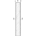
- 5, 6 and 7 are cross-sectional views schematically showing an intermediate product obtained in the process of manufacturing the bonded substrate of the first embodiment.
- steps S101 to S104 shown in FIG. 4 are sequentially executed.
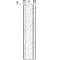
- step S101 as shown in FIG. 5, brazing material layers 171 and 172 are formed on the main surfaces 1101 and 1102 of the silicon nitride ceramic substrate 110, respectively.
- the formation of the brazing material layer 171 is omitted.
- the formation of the brazing material layer 172 is omitted.
- a paste containing an active metal brazing filler metal and a solvent is prepared.
- the paste may further contain binders, dispersants, defoamers and the like.
- the prepared paste is screen-printed on the main surfaces 1101 and 1102 of the silicon nitride ceramic substrate 110, and the first and second screen-printed films are formed on the main surfaces 1101 and 1102 of the silicon nitride ceramic substrate 110, respectively. Will be done.
- the solvent contained in the formed first and second screen printing films is volatilized. As a result, the first and second screen printing films are changed into the brazing material layers 171 and 172, respectively.
- the brazing filler metal layers 171 and 172 include an active metal brazing filler metal.
- the brazing filler metal layers 171 and 172 may be formed by a method different from this method.
- the active metal brazing material is at least one metal hydride powder selected from the group consisting of metal powders containing silver (Ag), copper (Cu) and indium (In), and titanium hydride powder and zirconium hydride powder. including.
- the composition of the active metal brazing may be changed. For example, both or one of copper and indium may not be contained in the metal powder, and a metal element other than copper and indium, such as tin (Sn), may be contained in the metal powder.
- the active metal brazing material preferably contains 40% by weight or more and 80% by weight or less of silver. Since the active metal brazing material contains only a small amount of silver in this way, it becomes easy to diffuse silver to the copper plates 131A and 132A and eliminate silver from the bonding layers 121B and 122B in the step S103 described below.
- the active metal brazing material preferably consists of a powder having an average particle size of 0.1 ⁇ m or more and 10 ⁇ m or less.
- the average particle size can be obtained by measuring the particle size distribution with a commercially available laser diffraction type particle size distribution measuring device and calculating D50 (median diameter) from the measured particle size distribution. Since the active metal brazing material is composed of a powder having such a small average particle size, the brazing material layers 171 and 172 can be thinned.
- the brazing filler metal layers 171 and 172 preferably have a thickness of 0.1 ⁇ m or more and 10 ⁇ m or less, and more preferably 0.1 ⁇ m or more and 5 ⁇ m or less. Since the brazing filler metal layers 171 and 172 have such a small thickness, the amount of silver contained in the brazing filler metal layers 171 and 172 is reduced, and silver is diffused and joined to the copper plates 131A and 132A in the step S103 described below. It facilitates the elimination of silver from layers 121B and 122B.
- step S102 copper plates 131A and 132A are arranged on the formed brazing filler metal layers 171 and 172, respectively.
- an intermediate product 100A including the silicon nitride ceramic substrate 110, the brazing material layer 171 and the copper plate 131A, the brazing material layer 172 and the copper plate 132A can be obtained.
- the bonding layer 121 and the copper plate 131 are omitted from the bonding substrate 100
- the arrangement of the copper plate 131A is omitted.
- the bonding layer 122 and the copper plate 132 are omitted from the bonding substrate 100
- the arrangement of the copper plate 132A is omitted.
- step S103 the obtained intermediate product 100A is heat-treated.
- the brazing material layers 171 and 172 are changed to the bonding layers 121B and 122B, respectively, as shown in FIG. 7, and the silicon nitride ceramic substrate 110, the bonding layer 121B, the copper plate 131A, the bonding layer 122B and the copper plate 132A are formed.
- An intermediate product 100B to be provided is obtained.
- the bonding layers 121B and 122B bond the copper plates 131A and 132A to the silicon nitride ceramic substrate 110, respectively.
- each of the copper plates 131A and 132A has a first thickness direction region 151 containing silver and having a first silver concentration, and a second thickness having a second silver concentration lower than the first silver concentration.
- the directional region 152 is formed.
- hot pressing is performed on the intermediate product 100A.
- the silicon nitride ceramic substrate is subjected to a surface pressure profile in which the intermediate product 100A has a maximum surface pressure of 5 MPa or more and 25 MPa or less in a vacuum or an inert gas. It is pressurized in the thickness direction of 110 and heated according to a temperature profile having a maximum temperature of 800 ° C. or higher and 900 ° C. or lower.
- the copper plates 131A and 132A are made of silicon nitride without forming voids. It can be bonded to the ceramic substrate 110. Further, since the brazing filler metal layers 171 and 172 can be thinned without forming voids, the amount of silver contained in the brazing filler metal layers 171 and 172 can be reduced, and the silver is diffused to the copper plates 131A and 132A to form a bonding layer. It becomes easy to eliminate silver from 121B and 122B.
- the shape of the particles constituting the active metal brazing material changes to a layered shape, and silver or the like diffuses into the copper plates 131A and 132A, so that the bonding layers 121B and 122B are substantially 0.1 ⁇ m or more and 5 ⁇ m or less. Will have the thickness of.
- step S104 the bonding layer 121B, the copper plate 131A, the bonding layer 122B, and the copper plate 132A are patterned.
- the bonding layers 121B and 122B are changed to the patterned bonding layers 121 and 122 shown in FIG. 1, respectively.
- the copper plates 131A and 132A are changed to the patterned copper plates 131 and 132 shown in FIG. 1, respectively.
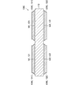
- FIG. 8 is a flowchart showing the flow of patterning of the bonded layer and the copper plate in the production of the bonded substrate of the first embodiment.
- 9 and 10 are cross-sectional views schematically illustrating an intermediate product obtained in the process of patterning the bonding layer and the copper plate in the production of the bonding substrate of the first embodiment.
- the steps S111 to S113 shown in FIG. 8 are sequentially executed.
- step S111 the copper plates 131A and 132A are hard-etched. As a result, a part of the copper plates 131A and 132A is removed, and as shown in FIG. 9, the copper plates 131A and 132A are changed to the etched copper plates 131C and 132C, respectively. Further, on the bonding layer 121B, a first portion 181 between the silicon nitride ceramics substrate 110 and the etched copper plate 131C and a second portion not between the silicon nitride ceramics substrate 110 and the etched copper plate 131C are formed. 191 is formed.
- a first portion 182 between the silicon nitride ceramic substrate 110 and the etched copper plate 132C and a second portion not between the silicon nitride ceramic substrate 110 and the etched copper plate 132C are formed.
- 192 is formed.
- an etching solution such as an iron chloride aqueous solution system or a copper chloride aqueous solution system can be used.
- step S112 as shown in FIG. 10, the formed second portions 191 and 192 are etched. As a result, the second portions 191 and 192 are removed, leaving the first portions 181 and 182. The remaining first portions 181 and 182 become the bonding layers 121 and 122, respectively. As a result, an intermediate product 100C including a silicon nitride ceramic substrate 110, a bonding layer 121, a copper plate 131C, a bonding layer 122 and a copper plate 132C can be obtained. An etching solution such as an aqueous ammonium fluoride solution can be used for etching the second portions 191 and 192. In step S112, both ends of the first portions 181 and 182 may be removed by etching.
- step S113 the etched copper plates 131C and 132C are soft-etched. As a result, the vicinity of the end portions of the etched copper plates 131C and 132C is removed. Further, the etched copper plates 131C and 132C are changed to the patterned copper plates 131 and 132 shown in FIG. 1, respectively. Further, an inter-plate portion 160 and a protruding portion 161 shown in FIG. 1 are formed in each of the bonding layers 121 and 122.
- an etching solution such as an iron chloride aqueous solution system or a copper chloride aqueous solution system can be used. In step S113, even when both ends of the first portions 181 and 182 are removed by etching in step S112, the protruding portion 161 can be reliably formed.
- the first thickness-direction region 151 having the first silver concentration is etched at the first etching rate.
- the second thickness direction region 152 having a second silver concentration lower than the first silver concentration is etched at a second etching rate faster than the first etching rate.
- bumps 1400 Effect of manufacturing conditions on bumps Whether or not bumps 1400 are formed and the shape of bumps 1400 formed mainly depend on the amount of silver diffused into the copper plates 131A and 132A and the severity of soft etching. To do. Therefore, when the bonded substrate 100 is manufactured, the manufacturing conditions that affect the amount of silver diffused into the copper plates 131A and 132A and the severity of soft etching so that the bump 1400 having an appropriate shape is formed. Is determined.
- the hump 1400 having the shape shown in FIG. 3 is easily formed because it is easily formed. Further, it is considered that the higher the severity of the soft etching, the easier it is for the bump 1400 to be formed, and the easier it is for the bump 1400 having the shape shown in FIG. 3 to be formed.
- Increasing the amount of silver diffused into the copper plates 131A and 132A means thickening the brazing filler metal layers 171 and 172, increasing the concentration of silver contained in the active metal brazing filler metal, and heat-treating the intermediate product 100A. It can be realized by raising the temperature at the time of performing.
- Increasing the severity of soft etching means increasing the temperature of the etching solution used for soft etching, increasing the concentration of iron chloride, copper chloride, etc. contained in the etching solution used for soft etching, and soft etching. This can be realized by lengthening the time for contacting the copper plates 131C and 132C with the etching solution used in the above.
- Example 1-17 the bonded substrate 100 was manufactured according to the method for manufacturing the bonded substrate 100 described above.
- Example 1-17 copper plates 131 and 132 having a thickness of 0.8 mm were bonded to the silicon nitride ceramic substrate 110 having a thickness of 0.32 mm. Further, brazing material layers 171 and 172 having a thickness of 0.1 ⁇ m or more and 5 ⁇ m or less and containing 40% by weight or more and 80% by weight or less of silver and an active metal brazing material containing titanium hydride were formed. In addition, hot pressing was performed on the intermediate product 100A. At that time, the intermediate product 100A was pressurized in vacuum according to the surface pressure profile having a maximum surface pressure of 20 MPa, and the intermediate product 100A was heated according to the temperature profile having a maximum temperature of 815 ° C. or higher and 845 ° C. or lower.
- hard etching was performed by spraying an etching solution having a temperature of about 45 ° C. toward the intermediate product 100B.
- soft etching was performed by immersing the intermediate product 100C in an etching solution of an aqueous iron chloride solution having a temperature of about 20 ° C. for 1.5 minutes or more and 5 minutes or less. Further, the distance L1 was set to 100 ⁇ m or less.
- Comparative Example 1 the bonded substrate 100 was manufactured in the same manner as in Example 1-17 except that soft etching was not performed.
- brazing filler layers 171 and 172 having a thickness of 0.1 ⁇ m or more and 1 ⁇ m or less and containing an active metal brazing material containing 40% by weight or less of silver and titanium hydride were formed.
- the point that soft etching was performed by heating the intermediate product 100A according to the temperature profile at which the maximum temperature is 800 ° C. or less and immersing the intermediate product 100C in an etching solution of an aqueous iron chloride solution for 0.5 minutes or more and 1 minute or less.
- a bonded substrate 100 was manufactured in the same manner as in Example 1-17 except for the above.
- brazing material layers 171 and 172 having a thickness of 5 ⁇ m or less and containing 60% by weight or more and 80% by weight or less of silver and an active metal brazing material containing titanium hydride were formed, and the maximum temperature was increased.
- Example 1- Except that the intermediate product 100A was heated according to a temperature profile of 900 ° C. or higher, and soft etching was performed by immersing the intermediate product 100C in an etching solution of an aqueous iron chloride solution for 1.5 minutes. The bonded substrate 100 was manufactured in the same manner as in 17.
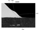
- the manufactured bonding substrate 100 was processed to expose the cross section of the bonding substrate 100, and the exposed cross section was observed with a scanning electron microscope (SEM) to obtain an SEM image. Further, the angle ⁇ 1, the angle ⁇ 2, and the distance L2 were specified from the obtained SEM image. The results are shown in Table 1.
- the durability of the first cold cycle of the manufactured bonded substrate 100 was evaluated.
- the bonded substrate 100 was exposed to a cold cycle of 3000 cycles. In each of the 3000 cycles of cooling and heating, the bonded substrate 100 was sequentially exposed to a low temperature of ⁇ 40 ° C. and a high temperature of 150 ° C. The results are shown in Table 1.
- the durability of the second cold cycle of the manufactured bonded substrate 100 was evaluated.
- the bonded substrate 100 was exposed to a cold cycle of 3000 cycles. In each of the 3000 cycles of cooling and heating, the bonded substrate 100 was sequentially exposed to a low temperature of ⁇ 55 ° C. and a high temperature of 175 ° C. The results are shown in Table 1.
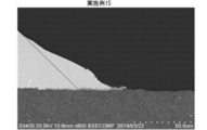
- Example 4 Example 15, Example 16 and Comparative Example 2 are shown in FIGS. 11, 12, 13, 14, and 15, respectively. ..
- the distances L1 are 40 ⁇ m (FIG. 11), 30 ⁇ m (FIG. 12), 50 ⁇ m (FIG. 13), and 41 ⁇ m (FIG. 14), respectively. ), 49 ⁇ m (FIG. 15).
- Example 1-2 in which the bump 1400 has the shape shown in FIG. 2, the angle ⁇ 1 is 135 ° or more and 165 ° or less, and the distance L2 is 10 ⁇ m or more, the first cold heat is obtained. It can be understood that the cycle durability is “OK” but the second thermal cycle durability is "NG”.
- Example 3-16 in which the bump 1400 has the shape shown in FIG. 3 the angles ⁇ 1 and ⁇ 2 are 135 ° or more and 165 ° or less, and the distance L2 is 10 ⁇ m or more.
- both the first cold cycle durability and the second cold cycle durability are "OK".
- the bump 1400 has the shape shown in FIG. 3, and the angles ⁇ 1 and ⁇ 2 are 135 ° or more and 165 ° or less, but in Comparative Example 2 in which the distance L2 is shorter than 10 ⁇ m. , It can be understood that both the first cold cycle durability and the second cold cycle durability are "NG".
- the bump 1400 has the shape shown in FIG. 3, but in Comparative Example 3 in which the angles ⁇ 1 and ⁇ 2 are larger than 165 ° and the distance L2 is shorter than 10 ⁇ m, the first cold heat is used. It can be understood that both the cycle durability and the second thermal cycle durability are "NG".
- the bump 1400 has the shape shown in FIG. 3, and the distance L2 is 10 ⁇ m or more, but in Comparative Example 4 in which the angles ⁇ 1 and ⁇ 2 are larger than 165 °, the first It can be understood that both the cold cycle durability of the above and the second cold cycle durability are "NG".
- the bump 1400 has the shape shown in FIG. 3, but in Comparative Example 5 in which the angles ⁇ 1 and ⁇ 2 are smaller than 135 ° and the distance L2 is shorter than 10 ⁇ m, the first cooling heat is obtained. It can be understood that both the cycle durability and the second thermal cycle durability are "NG".
Landscapes
- Engineering & Computer Science (AREA)
- Chemical & Material Sciences (AREA)
- Ceramic Engineering (AREA)
- Microelectronics & Electronic Packaging (AREA)
- Manufacturing & Machinery (AREA)
- Materials Engineering (AREA)
- Structural Engineering (AREA)
- Organic Chemistry (AREA)
- Inorganic Chemistry (AREA)
- Ceramic Products (AREA)
- Structure Of Printed Boards (AREA)
- Manufacturing Of Printed Wiring (AREA)
Abstract
La présente invention améliore la durabilité de cyclage thermique d'un substrat lié dans lequel une plaque de cuivre est liée à un substrat en céramique de nitrure de silicium par l'intermédiaire d'une couche de liaison. La plaque de cuivre et la couche de liaison sont disposées sur le substrat en céramique de nitrure de silicium. La plaque de cuivre a une seconde surface principale sur le côté opposé au côté d'une première surface principale de la plaque de cuivre, et est liée au substrat en céramique de nitrure de silicium au moyen de la couche de liaison. Une surface d'extrémité de la plaque de cuivre comprend une première partie et une seconde partie. La seconde partie est plus proche de la seconde surface principale que la première partie. La première partie et la seconde partie forment un angle de 135° à 165° inclus sur l'extérieur de la plaque de cuivre. La distance de la seconde surface principale à un point d'intersection de la première partie et de la seconde partie dans une direction d'épaisseur de la plaque de cuivre est de 10 µm à 100 µm inclus. La seconde surface principale s'étend au-delà d'une surface d'extension de la première partie d'une distance supérieure ou égale à 10 µm.
Priority Applications (6)
| Application Number | Priority Date | Filing Date | Title |
|---|---|---|---|
| PCT/JP2019/015414 WO2020208698A1 (fr) | 2019-04-09 | 2019-04-09 | Substrat lié et procédé permettant de fabriquer un substrat lié |
| EP20787489.2A EP3955284A4 (fr) | 2019-04-09 | 2020-03-30 | Substrat lié et procédé de production de substrat lié |
| PCT/JP2020/014514 WO2020209121A1 (fr) | 2019-04-09 | 2020-03-30 | Substrat lié et procédé de production de substrat lié |
| JP2021513580A JP7289911B2 (ja) | 2019-04-09 | 2020-03-30 | 接合基板及び接合基板の製造方法 |
| US17/494,891 US11917752B2 (en) | 2019-04-09 | 2021-10-06 | Bonded substrate and manufacturing method of bonded substrate |
| JP2022135729A JP7373038B2 (ja) | 2019-04-09 | 2022-08-29 | 接合基板 |
Applications Claiming Priority (1)
| Application Number | Priority Date | Filing Date | Title |
|---|---|---|---|
| PCT/JP2019/015414 WO2020208698A1 (fr) | 2019-04-09 | 2019-04-09 | Substrat lié et procédé permettant de fabriquer un substrat lié |
Publications (1)
| Publication Number | Publication Date |
|---|---|
| WO2020208698A1 true WO2020208698A1 (fr) | 2020-10-15 |
Family
ID=72751554
Family Applications (2)
| Application Number | Title | Priority Date | Filing Date |
|---|---|---|---|
| PCT/JP2019/015414 Ceased WO2020208698A1 (fr) | 2019-04-09 | 2019-04-09 | Substrat lié et procédé permettant de fabriquer un substrat lié |
| PCT/JP2020/014514 Ceased WO2020209121A1 (fr) | 2019-04-09 | 2020-03-30 | Substrat lié et procédé de production de substrat lié |
Family Applications After (1)
| Application Number | Title | Priority Date | Filing Date |
|---|---|---|---|
| PCT/JP2020/014514 Ceased WO2020209121A1 (fr) | 2019-04-09 | 2020-03-30 | Substrat lié et procédé de production de substrat lié |
Country Status (4)
| Country | Link |
|---|---|
| US (1) | US11917752B2 (fr) |
| EP (1) | EP3955284A4 (fr) |
| JP (2) | JP7289911B2 (fr) |
| WO (2) | WO2020208698A1 (fr) |
Families Citing this family (7)
| Publication number | Priority date | Publication date | Assignee | Title |
|---|---|---|---|---|
| JPWO2024204804A1 (fr) | 2023-03-31 | 2024-10-03 | ||
| EP4693390A1 (fr) | 2023-03-31 | 2026-02-11 | NGK Insulators, Ltd. | Substrat de dispositif à semi-conducteur et procédé de production de substrat de dispositif à semi-conducteur |
| EP4539118A1 (fr) * | 2023-05-22 | 2025-04-16 | LX Semicon Co., Ltd. | Procédé de fabrication d'un substrat de dissipation de chaleur pour un module semi-conducteur de puissance et procédé de fabrication d'un module semi-conducteur de puissance le comprenant |
| EP4593075A1 (fr) * | 2024-01-24 | 2025-07-30 | Heraeus Electronics GmbH & Co. KG | Substrat métal-céramique avec zone de contact |
| EP4593076A1 (fr) * | 2024-01-24 | 2025-07-30 | Heraeus Electronics GmbH & Co. KG | Substrat métal-céramique avec zone de contact |
| WO2026038576A1 (fr) * | 2024-08-16 | 2026-02-19 | 株式会社Niterra Materials | Carte de circuit imprimé en céramique |
| WO2026038575A1 (fr) * | 2024-08-16 | 2026-02-19 | 株式会社Niterra Materials | Procédé de production de carte de circuit imprimé en céramique |
Citations (5)
| Publication number | Priority date | Publication date | Assignee | Title |
|---|---|---|---|---|
| JP2005116843A (ja) * | 2003-10-09 | 2005-04-28 | Hitachi Metals Ltd | 回路用金属板およびセラミックス回路基板 |
| JP2005268821A (ja) * | 2005-05-24 | 2005-09-29 | Hitachi Metals Ltd | セラミックス回路基板及びこれを用いたパワー半導体モジュール |
| WO2013002407A1 (fr) * | 2011-06-30 | 2013-01-03 | 日立金属株式会社 | Métal d'apport de brasage, pâte métallique d'apport de brasage, substrat pour circuit céramique, substrat pour circuit maître céramique, et module d'alimentation à semi-conducteurs |
| JP2013030609A (ja) * | 2011-07-28 | 2013-02-07 | Showa Denko Kk | 電子素子搭載用基板 |
| JP2016174165A (ja) * | 2011-12-20 | 2016-09-29 | 株式会社東芝 | 半導体装置 |
Family Cites Families (9)
| Publication number | Priority date | Publication date | Assignee | Title |
|---|---|---|---|---|
| JP4493158B2 (ja) * | 2000-05-29 | 2010-06-30 | 京セラ株式会社 | セラミック回路基板 |
| JP2005116813A (ja) | 2003-10-08 | 2005-04-28 | Toshiba Corp | 電子デバイスの製造方法 |
| EP3273755B1 (fr) | 2009-09-15 | 2018-11-07 | Kabushiki Kaisha Toshiba | Procédé de fabrication d'une carte de circuit céramique |
| JP5835696B2 (ja) * | 2012-09-05 | 2015-12-24 | 株式会社東芝 | 半導体装置およびその製造方法 |
| US20150279793A1 (en) * | 2014-03-27 | 2015-10-01 | Taiwan Semiconductor Manufacturing Company Ltd. | Semiconductor structure and manufacturing method thereof |
| EP3358614B1 (fr) * | 2015-09-28 | 2022-12-14 | Kabushiki Kaisha Toshiba | Substrat de circuit et dispositif à semi-conducteur |
| JP6619277B2 (ja) | 2016-03-28 | 2019-12-11 | 京セラ株式会社 | 放熱用部材およびこれを用いたモジュール |
| DE112018000457T5 (de) * | 2017-02-23 | 2019-09-26 | Ngk Insulators, Ltd. | Isoliertes wärmeableitungssubstrat |
| US10522468B2 (en) * | 2017-07-31 | 2019-12-31 | Taiwan Semiconductor Manufacturing Company, Ltd. | Interconnect structure and method |
-
2019
- 2019-04-09 WO PCT/JP2019/015414 patent/WO2020208698A1/fr not_active Ceased
-
2020
- 2020-03-30 EP EP20787489.2A patent/EP3955284A4/fr active Pending
- 2020-03-30 WO PCT/JP2020/014514 patent/WO2020209121A1/fr not_active Ceased
- 2020-03-30 JP JP2021513580A patent/JP7289911B2/ja active Active
-
2021
- 2021-10-06 US US17/494,891 patent/US11917752B2/en active Active
-
2022
- 2022-08-29 JP JP2022135729A patent/JP7373038B2/ja active Active
Patent Citations (5)
| Publication number | Priority date | Publication date | Assignee | Title |
|---|---|---|---|---|
| JP2005116843A (ja) * | 2003-10-09 | 2005-04-28 | Hitachi Metals Ltd | 回路用金属板およびセラミックス回路基板 |
| JP2005268821A (ja) * | 2005-05-24 | 2005-09-29 | Hitachi Metals Ltd | セラミックス回路基板及びこれを用いたパワー半導体モジュール |
| WO2013002407A1 (fr) * | 2011-06-30 | 2013-01-03 | 日立金属株式会社 | Métal d'apport de brasage, pâte métallique d'apport de brasage, substrat pour circuit céramique, substrat pour circuit maître céramique, et module d'alimentation à semi-conducteurs |
| JP2013030609A (ja) * | 2011-07-28 | 2013-02-07 | Showa Denko Kk | 電子素子搭載用基板 |
| JP2016174165A (ja) * | 2011-12-20 | 2016-09-29 | 株式会社東芝 | 半導体装置 |
Also Published As
| Publication number | Publication date |
|---|---|
| EP3955284A1 (fr) | 2022-02-16 |
| US20220030708A1 (en) | 2022-01-27 |
| JP7373038B2 (ja) | 2023-11-01 |
| US11917752B2 (en) | 2024-02-27 |
| JP7289911B2 (ja) | 2023-06-12 |
| JPWO2020209121A1 (fr) | 2020-10-15 |
| JP2022173209A (ja) | 2022-11-18 |
| WO2020209121A1 (fr) | 2020-10-15 |
| EP3955284A4 (fr) | 2023-09-20 |
Similar Documents
| Publication | Publication Date | Title |
|---|---|---|
| JP7289911B2 (ja) | 接合基板及び接合基板の製造方法 | |
| CN104011852B (zh) | 陶瓷铜电路基板和使用了陶瓷铜电路基板的半导体装置 | |
| EP3398205B1 (fr) | Substrat lié et procédé permettant de fabriquer un substrat lié | |
| KR102324373B1 (ko) | 방열판 및 그 제조 방법 | |
| WO2019221174A1 (fr) | Carte de circuit en cuivre céramique et procédé de fabrication associé | |
| JP7471376B2 (ja) | 回路基板及び半導体装置 | |
| JP2021132238A (ja) | 回路基板および半導体モジュール | |
| WO2017056666A1 (fr) | Carte de circuit imprimé de nitrure de silicium et module semi-conducteur l'utilisant | |
| US20210387923A1 (en) | Bonded substrate | |
| JP7289910B2 (ja) | 接合基板及び接合基板の製造方法 | |
| WO2016111206A1 (fr) | Substrat de dissipation thermique | |
| TWI636719B (zh) | 結合金屬與陶瓷基板的製造方法 | |
| JPH08274423A (ja) | セラミックス回路基板 | |
| KR102529238B1 (ko) | 세라믹 기판 및 이의 제조방법 | |
| JP2025085780A (ja) | 回路基板および半導体モジュールの製造方法 | |
| WO2024204804A1 (fr) | Substrat pour dispositif à semi-conducteur | |
| WO2025216198A1 (fr) | Corps lié en céramique-cuivre, carte de circuit imprimé en céramique-cuivre et procédé de production d'un corps lié en céramique-cuivre | |
| WO2025134898A1 (fr) | Carte de circuits imprimés céramique et son procédé de fabrication | |
| WO2024154827A1 (fr) | Substrat au nitrure de silicium et carte de circuit imprimé au nitrure de silicium correspondante | |
| KR20220103956A (ko) | 복합 기판 및 그 제조 방법, 및 회로 기판 및 그 제조 방법 | |
| JP2018060885A (ja) | 半導体装置の製造方法 | |
| JP2026006113A (ja) | 接合体及びその製造方法、並びにパワーモジュール | |
| JP2018206879A (ja) | 電子部品収納用パッケージの製造方法および電子部品収納用パッケージ | |
| JP2018034168A (ja) | ハンダ接合体 |
Legal Events
| Date | Code | Title | Description |
|---|---|---|---|
| 121 | Ep: the epo has been informed by wipo that ep was designated in this application |
Ref document number: 19923843 Country of ref document: EP Kind code of ref document: A1 |
|
| NENP | Non-entry into the national phase |
Ref country code: DE |
|
| 122 | Ep: pct application non-entry in european phase |
Ref document number: 19923843 Country of ref document: EP Kind code of ref document: A1 |
|
| NENP | Non-entry into the national phase |
Ref country code: JP |