WO2020209295A1 - Lampe de véhicule et son circuit d'éclairage - Google Patents
Lampe de véhicule et son circuit d'éclairage Download PDFInfo
- Publication number
- WO2020209295A1 WO2020209295A1 PCT/JP2020/015845 JP2020015845W WO2020209295A1 WO 2020209295 A1 WO2020209295 A1 WO 2020209295A1 JP 2020015845 W JP2020015845 W JP 2020015845W WO 2020209295 A1 WO2020209295 A1 WO 2020209295A1
- Authority
- WO
- WIPO (PCT)
- Prior art keywords
- semiconductor light
- target amount
- temperature sensor
- lighting circuit
- light source
- Prior art date
- Legal status (The legal status is an assumption and is not a legal conclusion. Google has not performed a legal analysis and makes no representation as to the accuracy of the status listed.)
- Ceased
Links
Images




Classifications
-
- B—PERFORMING OPERATIONS; TRANSPORTING
- B60—VEHICLES IN GENERAL
- B60Q—ARRANGEMENT OF SIGNALLING OR LIGHTING DEVICES, THE MOUNTING OR SUPPORTING THEREOF OR CIRCUITS THEREFOR, FOR VEHICLES IN GENERAL
- B60Q1/00—Arrangement of optical signalling or lighting devices, the mounting or supporting thereof or circuits therefor
-
- H—ELECTRICITY
- H05—ELECTRIC TECHNIQUES NOT OTHERWISE PROVIDED FOR
- H05B—ELECTRIC HEATING; ELECTRIC LIGHT SOURCES NOT OTHERWISE PROVIDED FOR; CIRCUIT ARRANGEMENTS FOR ELECTRIC LIGHT SOURCES, IN GENERAL
- H05B45/00—Circuit arrangements for operating light-emitting diodes [LED]
- H05B45/20—Controlling the colour of the light
- H05B45/28—Controlling the colour of the light using temperature feedback
-
- H—ELECTRICITY
- H10—SEMICONDUCTOR DEVICES; ELECTRIC SOLID-STATE DEVICES NOT OTHERWISE PROVIDED FOR
- H10H—INORGANIC LIGHT-EMITTING SEMICONDUCTOR DEVICES HAVING POTENTIAL BARRIERS
- H10H20/00—Individual inorganic light-emitting semiconductor devices having potential barriers, e.g. light-emitting diodes [LED]
- H10H20/80—Constructional details
Definitions
- the present invention relates to a vehicle lamp used for an automobile or the like.
- Turquoise blue is defined as (0.0292, 0.3775), (0.2050, 0.3775), (0.1965, 0.3380), (0.0370, 0.3380) in the CIExy chromaticity diagram. It is included in the range surrounded by 4 points.
- the present invention has been made in such a situation, and one of the exemplary purposes of the embodiment is to provide a vehicle lamp capable of emitting light in turquoise blue.
- One aspect of the present invention relates to a lighting circuit that drives a blue first semiconductor light emitting device and a green second semiconductor light emitting device.
- the lighting circuit consists of a first drive circuit that supplies a first drive current stabilized to the first target amount to the first semiconductor light emitting element, and a second drive stabilized to the second target amount to the second semiconductor light emitting element.
- a second drive circuit for supplying an electric current is provided.
- the required turquoise light can be generated with high efficiency by mixing blue and green.
- the lighting circuit may further include a temperature sensor. At least one of the first target amount and the second target amount may change according to the output of the temperature sensor.
- the amount of light and the emission wavelength when the same drive current is supplied change according to the temperature. Therefore, by monitoring the temperature and correcting the balance between the first target amount and the second target amount according to the temperature fluctuation, the required turquoise blue can be generated even when the temperature fluctuation occurs.
- the first target amount is invariant with respect to the output of the temperature sensor, and the second target amount may change according to the output of the temperature sensor. Comparing the blue semiconductor light emitting device and the green semiconductor light emitting device, the latter has worse temperature characteristics. Therefore, the turquoise blue light can be stabilized by changing the second target amount according to the temperature so that the light amount and wavelength of the second semiconductor light emitting element do not change.
- the second target amount may be changed by analog dimming.
- Analog dimming is more advantageous than PWM (Pulse Width Modulation) dimming from the viewpoint of noise.
- the second target amount may be changed by PWM dimming.
- PWM dimming is advantageous.
- the first target amount and the second target amount may change with opposite polarities according to the output of the temperature sensor.
- this control is effective when the wavelength of the semiconductor light emitting device changes according to the temperature.
- the lighting circuit may further include a pulse modulator that generates a first pulse signal and a second pulse signal whose duty ratio changes complementarily according to the output of the temperature sensor.
- the first drive circuit may switch the first drive current according to the first pulse signal
- the second drive circuit may switch the second drive current according to the second pulse signal.
- the vehicle lamp may include a blue first semiconductor light emitting element, a green second semiconductor light emitting element, and any of the above-mentioned lighting circuits.
- the vehicle lighting equipment may be an LED socket.
- a turquoise light source can be provided.
- FIG. 6 (a) and 6 (b) are operation waveform diagrams of the vehicle lamp of FIG. It is a circuit diagram of the vehicle lighting equipment which concerns on Example 4.
- FIG. 6 (a) and 6 (b) are operation waveform diagrams of the vehicle lamp of FIG. It is a circuit diagram of the vehicle lighting equipment which concerns on Example 4.
- FIG. It is an operation waveform figure of the vehicle lamp of FIG. It is a circuit diagram of the vehicle lighting equipment which concerns on Example 5.
- the "state in which the member A is connected to the member B” means that the member A and the member B are physically directly connected, and the member A and the member B are electrically connected to each other. It also includes the case of being indirectly connected via other members, which does not substantially affect the connection state, or does not impair the functions and effects performed by the combination thereof.
- a state in which the member C is provided between the member A and the member B means that the member A and the member C, or the member B and the member C are directly connected, and their electricity. It also includes the case of being indirectly connected via other members, which does not substantially affect the connection state, or does not impair the functions and effects performed by the combination thereof.
- the reference numerals attached to electric signals such as voltage signals and current signals, or circuit elements such as resistors and capacitors have their respective voltage values, current values, resistance values and capacitance values as required. It shall be represented.
- FIG. 1 is a circuit diagram of a vehicle lamp 200 according to an embodiment.
- the vehicle lighting device 200 is mounted on an autonomous driving vehicle and emits light in turquoise blue, which indicates that the vehicle is being autonomously driven.
- the switch 4 is turned on during the automatic operation, and the DC voltage (input voltage) VIN from the battery 2 is supplied to the vehicle lamp 200.
- the vehicle lamp 200 lights up when the input voltage VIN is supplied.
- the vehicle lamp 200 includes a first semiconductor light source 202, a second semiconductor light source 204, and a lighting circuit 300.
- the first semiconductor light source 202 includes one or a plurality of blue semiconductor light emitting elements connected in series.
- the second semiconductor light source 204 includes one or a plurality of green semiconductor light emitting elements connected in series.
- the semiconductor light emitting element is preferably an LED (light emitting diode), but may be an LD (laser diode) or an organic EL (Electro Luminescence) element.
- a preferred aspect of the vehicle lamp 200 is a semiconductor light source that can be replaced with a normal product in the event of a failure such as a disconnection, like a conventional general-purpose light bulb type, and is called an LED socket.
- the vehicle lamp 200 is an LED socket in which a first semiconductor light source 202, a second semiconductor light source 204, a lighting circuit 300, a circuit board and a heat sink (not shown) are housed in one package, and is attached to and detached from a lamp body (not shown). Has a possible shape. Since the LED socket is a consumable item as well as a long life, it is strongly required to reduce the cost.
- the lighting circuit 300 includes a first drive circuit 310, a second drive circuit 320, and a temperature sensor 330.
- the first drive circuit 310 supplies the first semiconductor light source 202 with the first drive current I LED1 stabilized to the first target amount.
- the second drive circuit 320 supplies the second semiconductor light source 204 with the second drive current I LED2 stabilized to the second target amount.
- the temperature sensor 330 detects the temperature of at least one of the first semiconductor light source 202 and the second semiconductor light source 204.
- a thermistor, a thermocouple, a diode using a constant current biased diode in the forward direction, or the like can be used.
- the first drive circuit 310 and the second drive circuit 320 change at least one of the first target amount I REF1 and the second target amount I REF2 according to the output of the temperature sensor 330.
- the required turquoise light can be generated with high efficiency by mixing blue and green that can be generated with high efficiency.
- the amount of light and the emission wavelength when the same drive current is supplied change according to the temperature. Therefore, if the same drive current is supplied regardless of the temperature, the balance between blue and green will be lost, and the required turquoise blue cannot be obtained. Therefore, by providing a temperature sensor 330 that monitors the temperature of the semiconductor light emitting element and correcting the balance between the first target amount I REF1 and the second target amount I REF2 according to the temperature fluctuation of the light emitting element, the temperature fluctuation occurs. It will also be possible to generate the required turquoise blue.
- the present invention extends to various devices and methods grasped as a block diagram or a cross-sectional view of FIG. 1 or derived from the above description, and is not limited to a specific configuration.
- more specific configuration examples and examples will be described not to narrow the scope of the present invention but to help understanding the essence and operation of the invention and to clarify them.
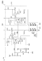
- FIG. 2 is a circuit diagram of the vehicle lamp 200A according to the first embodiment.
- the vehicle lamp 200A includes a first drive circuit 310, a second drive circuit 320, a temperature sensor 330, and a voltage source 340.
- the voltage source 340 produces a dimming voltage Vdim.
- Vdim dimming voltage
- the first drive circuit 310 includes a current source 312 and a conversion circuit 314.
- the current source 312 is a current source type driver and a V / I conversion circuit that is connected to the anode of the first semiconductor light source 202 and supplies the first drive current I LED1 proportional to the dimming voltage Vdim.
- the current source 312 includes a resistor R11, a transistor M11, and an error amplifier EA11.
- the target amount I REF1 of the first drive current I LED1 generated by the current source 312 is represented by the equation (1).
- I REF1 (V IN- Vy1) / R11 ... (1)
- the conversion circuit 314 converts the voltage Vdim with reference to the ground 304 into the voltage Vy1 with reference to the input line 302.
- the conversion circuit 314 includes a V / I conversion circuit 316 and a resistor R13.
- the V / I conversion circuit 316 includes a transistor Q12, a resistor R12, and an error amplifier EA12, and converts a voltage Vdim into a current Ix1.
- Ix1 Vdim / R12 ... (2)
- the second drive circuit 320 is configured in the same manner as the first drive circuit 310. Specifically, the second drive circuit 320 includes a current source 322 and a conversion circuit 324.
- the current source 322 has the same circuit configuration as the current source 312, and the conversion circuit 324 has the same circuit configuration as the conversion circuit 314.
- the target amount I REF2 of the second drive current I LED2 generated by the second drive circuit 320 is represented by the equation (5).
- I REF2 R23 / (R21 ⁇ R22) ⁇ Vdim... (5)
- the resistance value of the resistor R12 is individually adjusted in order to absorb the individual difference of the first semiconductor light source 202.
- the resistance value of the resistor R22 is individually adjusted in order to absorb the individual difference of the second semiconductor light source 204.
- the resistors R12 and R22 are chip parts, the resistors R12 and R22 having different resistance values are mounted for each vehicle lamp 200 (LED socket).
- the resistors R12 and R22 are integrated on an IC (Integrated Circuit) chip, they are adjusted to the optimum resistance value by a method such as laser trimming.
- the first target amount I REF1 of the first drive circuit 310 is invariant to the output of the temperature sensor 330, and the second target amount I REF2 of the second drive circuit 320 corresponds to the output of the temperature sensor 330. Change.
- the second target amount I REF2 is changed by analog dimming.
- the temperature sensor 330 is a thermistor 332 having a negative temperature coefficient and is arranged close to the second semiconductor light source 204 so that the temperature of the second semiconductor light source 204 can be detected.
- the thermistor 332 is connected in parallel with the resistor R22 of the second drive circuit 320.
- the target amount I REF2 of the second drive current I LED2 is represented by the equation (6).
- I REF2 R23 / (R21 x R22') x Vdim ... (6)
- R22' is the combined resistance of the resistor R22 and the thermistor 332.
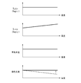
- FIG. 3 is a diagram illustrating the operation of the vehicle lamp 200A of FIG.
- the resistance value of the thermistor 332 decreases, and thus the combined resistance R22 decreases.
- the second target amount I REF2 of the formula (6) becomes larger as the temperature rises.
- the amount of light of the second semiconductor light source 204 when the same drive current I LED2 is supplied decreases as the temperature rises.
- the negative temperature coefficient of the amount of light of the second semiconductor light source 204 shown by the broken line in FIG. 3) can be offset, and the amount of light can be kept constant.
- the balance of the amount of light of the first semiconductor light source 202 and the second semiconductor light source 204 is maintained, and the color of turquoise blue obtained by mixing green and blue is defined in the specifications. It can be stored within the color range.
- the dimming voltage Vx may be constant regardless of the temperature, but in order to improve the reliability of the circuit at high temperature, the vehicle lamp 200A has a derating function at high temperature.
- the voltage source 340 lowers the dimming voltage Vdim as the temperature rises.
- the configuration of the voltage source 340 is not particularly limited, and includes, for example, resistors R31 to R33, a transistor Q31, and a thermistor RTH having a negative temperature coefficient. When the temperature rises, the resistance value of the thermistor RTH decreases, the collector current of the transistor Q31 increases, and the dimming voltage Vdim decreases.
- the dimming voltage Vdim decreases, the drive currents I LED1 and I LED2 decrease while maintaining their ratios. As a result, further temperature rise can be suppressed and the circuit can be protected.
- the ratio of the two drive currents I LED1 and I LED2 is maintained, so that the color of the turquoise light obtained by mixing the colors can be maintained.
- FIG. 4 is a circuit diagram of the vehicle lamp 200B according to the second embodiment.
- the second target amount I REF2 was changed by analog dimming, but in Example 2, the second target amount I REF2 was changed by PWM dimming.
- the vehicle lamp 200B includes a pulse modulator 350.
- Pulse modulator 350 generates a pulse signal S PWM2 having a duty ratio d 2 corresponding to the output of the temperature sensor 330.
- the second drive circuit 320 is configured to be able to switch the second drive current I LED2 supplied to the second semiconductor light source 204 in response to the pulse signal S PWM2 .
- a switch SW2 is provided between the gate of the transistor M21 and the input line 302 so that the switch SW2 is switched according to the pulse signal S PWM2 . It should be noted that the on period of the switch SW2 corresponds to the lighting of the second semiconductor light source 204, and the off period of the switch SW2 corresponds to the extinguishing of the second semiconductor light source 204. Therefore, the pulse signal S PWM2 is generated so that the higher the temperature detected by the temperature sensor 330, the longer the off time of the switch SW2.
- the position of the switch SW2 is not limited to that shown in FIG.
- the switch SW2 may be provided in parallel with the resistor R23.
- the dimming voltage Vdim may be individually generated for the first drive circuit 310 and the second drive circuit 320, and the dimming voltage Vdim for the second drive circuit 320 may be switched.
- a switch SW2 may be provided in parallel with the second semiconductor light source 204, and the switch SW2 may be switched according to the pulse signal S PWM2 .
- the target amount I REF2 of the drive current I LED2 is represented by the equation (7).
- I REF2 R23 / (R21 ⁇ R22) ⁇ Vdim ⁇ d... (7) Therefore, by changing the duty ratio d, the time average value of the amount of light of the second semiconductor light source 204 can be changed, thereby canceling out the temperature characteristics of the second semiconductor light source 204.
- the emission wavelength may shift according to the amount of current. If analog dimming is performed in such a case, not only the amount of light of the second semiconductor light source 204 but also the wavelength of green shifts, which may deviate from the specifications of turquoise blue. In such a case, by adopting PWM dimming, it is possible to change only the amount of light while keeping the wavelength (spectral distribution) constant.
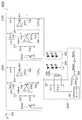
- FIG. 5 is a circuit diagram of the vehicle lamp 100C according to the third embodiment.
- the first target amount I REF1 changes according to the output of the temperature sensor 330. More specifically, the first target amount I REF1 and the second target amount I REF2 are complementarily changed by PWM dimming.
- the pulse modulator 350C generates a first pulse signal S PWM1 and a second pulse signal S PWM2 in which the duty ratio changes complementarily according to the output of the temperature sensor 330. Specifically, the duty ratio d 1 of the first pulse signal S PWM1 has a negative correlation with temperature, the duty ratio d 2 of the second pulse signal S PWM2 has a positive correlation with temperature.
- the pulse modulator 350C includes an oscillator 352, a PWM comparator 354, an inverter 356, R41, and R42.
- the thermistor 332, which is the temperature sensor 330, is connected in parallel with the resistor R42.
- a duty ratio setting voltage Vduty having a negative correlation with temperature is generated at the connection node of the resistors R41 and R42.
- Oscillator 352 produces a periodic or sawtooth wave periodic signal V OSC .
- the PWM comparator 354 slices the periodic signal V OSC with the voltage Vduty to generate the second pulse signal S PWM2 .
- the inverter 356 inverts the second pulse signal S PWM2 to generate the first pulse signal S PWM1 .
- the first drive circuit 310C includes a first switch SW21 for PWM dimming in addition to the first drive circuit 310 of FIG. The first switch SW21 switches in response to the first pulse signal S PWM1 . Further, the second drive circuit 320C includes a second switch SW22 for PWM dimming in addition to the second drive circuit 320 of FIG. The second switch SW22 switches in response to the second pulse signal S PWM2 .
- connection location of the switch SW21 is not limited to that shown in FIG. 5, and may be provided in parallel with the resistor R11 (R21) or in parallel with the resistor R13 (R23). Alternatively, it may be provided between the gate of the transistor 11 (M21) and the input line 302.
- the first drive circuit 310 switches the first drive current I LED1 in response to the first pulse signal S PWM1
- the second drive circuit 320 switches the second drive current I LED2 in response to the second pulse signal S PWM2. To do.
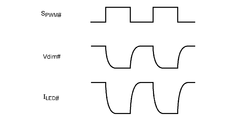
- FIG. 6A and 6 (b) are operation waveform diagrams of the vehicle lamp 200C of FIG.
- FIG. 6A shows the operation at low temperature
- FIG. 6B shows the operation at high temperature.
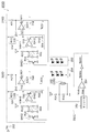
- FIG. 7 is a circuit diagram of the vehicle lamp 200D according to the fourth embodiment.
- the first drive circuit 310D further includes a capacitor C11 in parallel with the resistor R32 and a resistor R14 in series with the switch SW21.
- the second drive circuit 320D further includes a capacitor C21 in parallel with the resistor R34 and a resistor R24 in series with the switch SW22.
- FIG. 8 is an operation waveform diagram of the vehicle lamp 200D of FIG. 7.
- FIG. 9 is a circuit diagram of the vehicle lamp 200E according to the fifth embodiment.
- temperature sensors 330_1 and 330_1 that monitor the temperatures of the first semiconductor light source 202 and the second semiconductor light source 204 are provided.
- Pulse modulator 350_1 generates a first pulse signal S PWM1 having a duty ratio d 1 in accordance with the output of the temperature sensor 330_1.
- the pulse modulator 350_2 generates a second pulse signal S PWM2 having a duty ratio d 2 corresponding to the output of the temperature sensor 330_2.
- the first drive circuit 310 switches the first drive current I LED1 in response to the first pulse signal S PWM1
- the second drive circuit 320 switches the second drive current I LED2 in response to the second pulse signal S PWM2.
- the arrangement of the switches SW21 and SW22 for PWM dimming is not limited to that shown in FIG.
- the green second semiconductor light source 204 and the second drive circuit 320 may be omitted, and instead, a phosphor that is excited by the output of the first semiconductor light source 202 and emits green light may be provided. Turquoise blue can be obtained by mixing the green light emitted by the phosphor and the blue light that is the output of the first semiconductor light source 202.
- the target amount I REF2 of the second semiconductor light source 204 may be constant regardless of the output of the temperature sensor 330, and the target amount I REF1 of the first semiconductor light source 202 may be changed according to the output of the temperature sensor 330.
- the present invention relates to a vehicle lamp used for an automobile or the like.
- Vehicle lighting equipment 202 1st semiconductor light source 204 2nd semiconductor light source 300 Lighting circuit 310 1st drive circuit 312 Current source 314 Conversion circuit 316 V / I conversion circuit 320 2nd drive circuit 322 Current source 324 Conversion circuit 330 Temperature sensor 332 Thermista 340 Voltage source 350 Pulse modulator 352 Oscillator 354 PWM comparator
Landscapes
- Engineering & Computer Science (AREA)
- Mechanical Engineering (AREA)
- Circuit Arrangement For Electric Light Sources In General (AREA)
- Lighting Device Outwards From Vehicle And Optical Signal (AREA)
Abstract
La présente invention concerne un circuit d'éclairage (300) pour commander une première source de lumière à semi-conducteur (202) bleue et une seconde source de lumière à semi-conducteur (204) verte. Un premier circuit d'attaque (310) fournit à la première source de lumière à semi-conducteur (202) un premier courant d'attaque ILED1 stabilisé à une première quantité cible IREF1. Un second circuit d'attaque (320) fournit à la seconde source de lumière à semi-conducteur (204) un second courant d'attaque ILED2 stabilisé à une seconde quantité cible IREF2. Le circuit d'éclairage (300) fait varier, en fonction de la sortie d'un capteur de température (330), l'équilibre relatif entre la première quantité cible IREF1 et la seconde quantité cible IREF2.
Priority Applications (1)
| Application Number | Priority Date | Filing Date | Title |
|---|---|---|---|
| JP2021513675A JP7353358B2 (ja) | 2019-04-11 | 2020-04-08 | 車両用灯具およびその点灯回路 |
Applications Claiming Priority (2)
| Application Number | Priority Date | Filing Date | Title |
|---|---|---|---|
| JP2019075858 | 2019-04-11 | ||
| JP2019-075858 | 2019-04-11 |
Publications (1)
| Publication Number | Publication Date |
|---|---|
| WO2020209295A1 true WO2020209295A1 (fr) | 2020-10-15 |
Family
ID=72751303
Family Applications (1)
| Application Number | Title | Priority Date | Filing Date |
|---|---|---|---|
| PCT/JP2020/015845 Ceased WO2020209295A1 (fr) | 2019-04-11 | 2020-04-08 | Lampe de véhicule et son circuit d'éclairage |
Country Status (2)
| Country | Link |
|---|---|
| JP (1) | JP7353358B2 (fr) |
| WO (1) | WO2020209295A1 (fr) |
Cited By (5)
| Publication number | Priority date | Publication date | Assignee | Title |
|---|---|---|---|---|
| WO2022090430A1 (fr) * | 2020-10-30 | 2022-05-05 | Valeo Vision | Procédé de fonctionnement d'un dispositif d'éclairage automobile et dispositif d'éclairage automobile |
| WO2023286545A1 (fr) * | 2021-07-16 | 2023-01-19 | 株式会社小糸製作所 | Lampe |
| JP2023013626A (ja) * | 2021-07-16 | 2023-01-26 | 株式会社小糸製作所 | 灯具 |
| JP2023017175A (ja) * | 2021-07-26 | 2023-02-07 | 株式会社小糸製作所 | 灯具 |
| US12486953B2 (en) * | 2022-04-26 | 2025-12-02 | Koito Manufacturing Co., Ltd. | Lighting device |
Citations (6)
| Publication number | Priority date | Publication date | Assignee | Title |
|---|---|---|---|---|
| JP2003178611A (ja) * | 2001-12-12 | 2003-06-27 | Koito Mfg Co Ltd | 灯具組立装置 |
| JP2006171693A (ja) * | 2004-11-19 | 2006-06-29 | Sony Corp | バックライト装置、バックライト駆動方法及び液晶表示装置 |
| JP2012164594A (ja) * | 2011-02-09 | 2012-08-30 | Panasonic Corp | 半導体発光素子の点灯装置およびそれを用いた照明器具 |
| JP2017010810A (ja) * | 2015-06-23 | 2017-01-12 | ローム株式会社 | 照明装置、そのコントロール回路、制御方法、ならびにそれを用いたディスプレイ装置 |
| JP2017054799A (ja) * | 2015-09-10 | 2017-03-16 | パナソニックIpマネジメント株式会社 | 照明装置及びそれを備えた照明システム、移動体 |
| JP2017143692A (ja) * | 2016-02-12 | 2017-08-17 | ローム株式会社 | 液晶バックライト用ledの駆動回路、その制御回路、電子機器 |
-
2020
- 2020-04-08 WO PCT/JP2020/015845 patent/WO2020209295A1/fr not_active Ceased
- 2020-04-08 JP JP2021513675A patent/JP7353358B2/ja active Active
Patent Citations (6)
| Publication number | Priority date | Publication date | Assignee | Title |
|---|---|---|---|---|
| JP2003178611A (ja) * | 2001-12-12 | 2003-06-27 | Koito Mfg Co Ltd | 灯具組立装置 |
| JP2006171693A (ja) * | 2004-11-19 | 2006-06-29 | Sony Corp | バックライト装置、バックライト駆動方法及び液晶表示装置 |
| JP2012164594A (ja) * | 2011-02-09 | 2012-08-30 | Panasonic Corp | 半導体発光素子の点灯装置およびそれを用いた照明器具 |
| JP2017010810A (ja) * | 2015-06-23 | 2017-01-12 | ローム株式会社 | 照明装置、そのコントロール回路、制御方法、ならびにそれを用いたディスプレイ装置 |
| JP2017054799A (ja) * | 2015-09-10 | 2017-03-16 | パナソニックIpマネジメント株式会社 | 照明装置及びそれを備えた照明システム、移動体 |
| JP2017143692A (ja) * | 2016-02-12 | 2017-08-17 | ローム株式会社 | 液晶バックライト用ledの駆動回路、その制御回路、電子機器 |
Cited By (13)
| Publication number | Priority date | Publication date | Assignee | Title |
|---|---|---|---|---|
| JP2023545146A (ja) * | 2020-10-30 | 2023-10-26 | ヴァレオ ビジョン | 自動車両の照明装置を作動させるための方法および自動車両の照明装置 |
| FR3115859A1 (fr) * | 2020-10-30 | 2022-05-06 | Valeo Vision | Procédé de fonctionnement d'un dispositif d'éclairage automobile et dispositif d'éclairage automobile |
| US12289809B2 (en) | 2020-10-30 | 2025-04-29 | Valeo Vision | Method for operating an automotive lighting device and automotive lighting device |
| WO2022090430A1 (fr) * | 2020-10-30 | 2022-05-05 | Valeo Vision | Procédé de fonctionnement d'un dispositif d'éclairage automobile et dispositif d'éclairage automobile |
| JP7575587B2 (ja) | 2020-10-30 | 2024-10-29 | ヴァレオ ビジョン | 自動車両の照明装置を作動させるための方法および自動車両の照明装置 |
| JP2023013626A (ja) * | 2021-07-16 | 2023-01-26 | 株式会社小糸製作所 | 灯具 |
| EP4373217A4 (fr) * | 2021-07-16 | 2024-10-23 | Koito Manufacturing Co., Ltd. | Lampe |
| WO2023286545A1 (fr) * | 2021-07-16 | 2023-01-19 | 株式会社小糸製作所 | Lampe |
| JP7732788B2 (ja) | 2021-07-16 | 2025-09-02 | 株式会社小糸製作所 | 灯具 |
| US12526906B2 (en) | 2021-07-16 | 2026-01-13 | Koito Manufacturing Co., Ltd. | Lamp |
| JP7535017B2 (ja) | 2021-07-26 | 2024-08-15 | 株式会社小糸製作所 | 灯具 |
| JP2023017175A (ja) * | 2021-07-26 | 2023-02-07 | 株式会社小糸製作所 | 灯具 |
| US12486953B2 (en) * | 2022-04-26 | 2025-12-02 | Koito Manufacturing Co., Ltd. | Lighting device |
Also Published As
| Publication number | Publication date |
|---|---|
| JPWO2020209295A1 (fr) | 2020-10-15 |
| JP7353358B2 (ja) | 2023-09-29 |
Similar Documents
| Publication | Publication Date | Title |
|---|---|---|
| JP7353358B2 (ja) | 車両用灯具およびその点灯回路 | |
| KR101806533B1 (ko) | Led의 디밍 레벨을 제어하는 방법 및 디바이스 | |
| US8274237B2 (en) | LED driver circuit with over-current protection during a short circuit condition | |
| RU2622388C2 (ru) | Самонастраивающийся драйвер освещения для возбуждения источников света и осветительное устройство, включающее в себя самонастраивающийся драйвер освещения | |
| CN102858043B (zh) | 半导体光源点亮电路 | |
| JP7182925B2 (ja) | 車両用灯具 | |
| US10485075B2 (en) | Automotive lamp with compensation of the luminous flux of the light source | |
| JP2015153526A (ja) | 車両用灯具およびその駆動装置、その制御方法 | |
| US20090058318A1 (en) | Driving Device for Providing Light Dimming Control of Light-Emitting Element | |
| WO2021206145A1 (fr) | Monture de lampe de véhicule et circuit d'éclairage | |
| JP5963079B2 (ja) | Led駆動装置、照明装置および車両用照明装置 | |
| US11197356B2 (en) | Lighting circuit and vehicle lamp | |
| CN112566817A (zh) | 点亮电路及车辆用灯具 | |
| CN113710537B (zh) | 车辆用灯具及其点亮电路 | |
| JP5416356B2 (ja) | 車両用灯具 | |
| US9462652B2 (en) | Device for LED operation | |
| US20220353966A1 (en) | Lighting circuit | |
| JP5172500B2 (ja) | 駆動装置 | |
| JP6481246B2 (ja) | 発光装置の制御回路および発光装置 | |
| JP5945819B2 (ja) | Led点灯装置及びそれを用いた車両用照明装置並びに照明器具 | |
| JP2024062291A (ja) | 点灯回路および車両用灯具 | |
| KR101067976B1 (ko) | 발광소자 구동장치 | |
| JP2016068707A (ja) | 点灯回路およびそれを用いた車両用灯具 | |
| JP2007015579A (ja) | 車両用灯具 |
Legal Events
| Date | Code | Title | Description |
|---|---|---|---|
| 121 | Ep: the epo has been informed by wipo that ep was designated in this application |
Ref document number: 20787630 Country of ref document: EP Kind code of ref document: A1 |
|
| ENP | Entry into the national phase |
Ref document number: 2021513675 Country of ref document: JP Kind code of ref document: A |
|
| NENP | Non-entry into the national phase |
Ref country code: DE |
|
| 122 | Ep: pct application non-entry in european phase |
Ref document number: 20787630 Country of ref document: EP Kind code of ref document: A1 |