WO2020234998A1 - 電力変換装置 - Google Patents
電力変換装置 Download PDFInfo
- Publication number
- WO2020234998A1 WO2020234998A1 PCT/JP2019/020106 JP2019020106W WO2020234998A1 WO 2020234998 A1 WO2020234998 A1 WO 2020234998A1 JP 2019020106 W JP2019020106 W JP 2019020106W WO 2020234998 A1 WO2020234998 A1 WO 2020234998A1
- Authority
- WO
- WIPO (PCT)
- Prior art keywords
- command
- arm
- communication
- information
- hub
- Prior art date
- Legal status (The legal status is an assumption and is not a legal conclusion. Google has not performed a legal analysis and makes no representation as to the accuracy of the status listed.)
- Ceased
Links
Images








Classifications
-
- H—ELECTRICITY
- H02—GENERATION; CONVERSION OR DISTRIBUTION OF ELECTRIC POWER
- H02M—APPARATUS FOR CONVERSION BETWEEN AC AND AC, BETWEEN AC AND DC, OR BETWEEN DC AND DC, AND FOR USE WITH MAINS OR SIMILAR POWER SUPPLY SYSTEMS; CONVERSION OF DC OR AC INPUT POWER INTO SURGE OUTPUT POWER; CONTROL OR REGULATION THEREOF
- H02M7/00—Conversion of AC power input into DC power output; Conversion of DC power input into AC power output
- H02M7/42—Conversion of DC power input into AC power output without possibility of reversal
- H02M7/44—Conversion of DC power input into AC power output without possibility of reversal by static converters
- H02M7/48—Conversion of DC power input into AC power output without possibility of reversal by static converters using discharge tubes with control electrode or semiconductor devices with control electrode
- H02M7/483—Converters with outputs that each can have more than two voltages levels
- H02M7/4835—Converters with outputs that each can have more than two voltages levels comprising two or more cells, each including a switchable capacitor, the capacitors having a nominal charge voltage which corresponds to a given fraction of the input voltage, and the capacitors being selectively connected in series to determine the instantaneous output voltage
-
- H—ELECTRICITY
- H02—GENERATION; CONVERSION OR DISTRIBUTION OF ELECTRIC POWER
- H02M—APPARATUS FOR CONVERSION BETWEEN AC AND AC, BETWEEN AC AND DC, OR BETWEEN DC AND DC, AND FOR USE WITH MAINS OR SIMILAR POWER SUPPLY SYSTEMS; CONVERSION OF DC OR AC INPUT POWER INTO SURGE OUTPUT POWER; CONTROL OR REGULATION THEREOF
- H02M7/00—Conversion of AC power input into DC power output; Conversion of DC power input into AC power output
- H02M7/02—Conversion of AC power input into DC power output without possibility of reversal
- H02M7/04—Conversion of AC power input into DC power output without possibility of reversal by static converters
- H02M7/12—Conversion of AC power input into DC power output without possibility of reversal by static converters using discharge tubes with control electrode or semiconductor devices with control electrode
- H02M7/21—Conversion of AC power input into DC power output without possibility of reversal by static converters using discharge tubes with control electrode or semiconductor devices with control electrode using devices of a triode or transistor type requiring continuous application of a control signal
- H02M7/217—Conversion of AC power input into DC power output without possibility of reversal by static converters using discharge tubes with control electrode or semiconductor devices with control electrode using devices of a triode or transistor type requiring continuous application of a control signal using semiconductor devices only
- H02M7/25—Conversion of AC power input into DC power output without possibility of reversal by static converters using discharge tubes with control electrode or semiconductor devices with control electrode using devices of a triode or transistor type requiring continuous application of a control signal using semiconductor devices only arranged for operation in series, e.g. for multiplication of voltage
-
- H—ELECTRICITY
- H02—GENERATION; CONVERSION OR DISTRIBUTION OF ELECTRIC POWER
- H02M—APPARATUS FOR CONVERSION BETWEEN AC AND AC, BETWEEN AC AND DC, OR BETWEEN DC AND DC, AND FOR USE WITH MAINS OR SIMILAR POWER SUPPLY SYSTEMS; CONVERSION OF DC OR AC INPUT POWER INTO SURGE OUTPUT POWER; CONTROL OR REGULATION THEREOF
- H02M1/00—Details of apparatus for conversion
- H02M1/32—Means for protecting converters other than automatic disconnection
-
- H—ELECTRICITY
- H04—ELECTRIC COMMUNICATION TECHNIQUE
- H04L—TRANSMISSION OF DIGITAL INFORMATION, e.g. TELEGRAPHIC COMMUNICATION
- H04L12/00—Data switching networks
- H04L12/28—Data switching networks characterised by path configuration, e.g. LAN [Local Area Networks] or WAN [Wide Area Networks]
- H04L12/42—Loop networks
- H04L12/437—Ring fault isolation or reconfiguration
-
- H—ELECTRICITY
- H04—ELECTRIC COMMUNICATION TECHNIQUE
- H04L—TRANSMISSION OF DIGITAL INFORMATION, e.g. TELEGRAPHIC COMMUNICATION
- H04L12/00—Data switching networks
- H04L12/28—Data switching networks characterised by path configuration, e.g. LAN [Local Area Networks] or WAN [Wide Area Networks]
- H04L12/44—Star or tree networks
-
- H—ELECTRICITY
- H04—ELECTRIC COMMUNICATION TECHNIQUE
- H04L—TRANSMISSION OF DIGITAL INFORMATION, e.g. TELEGRAPHIC COMMUNICATION
- H04L12/00—Data switching networks
- H04L12/28—Data switching networks characterised by path configuration, e.g. LAN [Local Area Networks] or WAN [Wide Area Networks]
- H04L12/42—Loop networks
- H04L2012/421—Interconnected ring systems
-
- Y—GENERAL TAGGING OF NEW TECHNOLOGICAL DEVELOPMENTS; GENERAL TAGGING OF CROSS-SECTIONAL TECHNOLOGIES SPANNING OVER SEVERAL SECTIONS OF THE IPC; TECHNICAL SUBJECTS COVERED BY FORMER USPC CROSS-REFERENCE ART COLLECTIONS [XRACs] AND DIGESTS
- Y02—TECHNOLOGIES OR APPLICATIONS FOR MITIGATION OR ADAPTATION AGAINST CLIMATE CHANGE
- Y02E—REDUCTION OF GREENHOUSE GAS [GHG] EMISSIONS, RELATED TO ENERGY GENERATION, TRANSMISSION OR DISTRIBUTION
- Y02E60/00—Enabling technologies; Technologies with a potential or indirect contribution to GHG emissions mitigation
- Y02E60/60—Arrangements for transfer of electric power between AC networks or generators via a high voltage DC link [HVCD]
Definitions
- the present disclosure relates to a power conversion device that converts power between alternating current and direct current.
- a modular multilevel converter (MMC: Modular Multilevel Converter) is known as a self-excited power converter used in a DC power transmission system.
- the modular multi-level converter has an upper arm connected to the high potential side DC terminal and a lower arm connected to the low potential side DC terminal for each phase of AC.
- Each arm is configured by connecting a plurality of submodules in a cascade.
- Patent Document 1 discloses a power conversion device including a power conversion circuit capable of converting alternating current to direct current or direct current to alternating current.
- the power conversion circuit has an arm configured by connecting a plurality of unit converters in series.
- the power converter is connected to a first control device that controls each unit converter in an integrated manner, a plurality of second control devices that are daisy-chained to the first control device, and a second control device. It further includes a third control device that controls each unit converter.
- Patent Document 1 a central control device and a plurality of intermediate control devices are connected.
- the communication frame transmitted from the central controller contains the target arm number, and the cell control unit of the intermediate controller owns the carrier when the target arm number 404 and the identification number of the arm to which it belongs are equal. Set the phase to the specified value. Therefore, in order to give a command to all the arms, the communication frame must be transmitted as many times as the number of arms.
- An object of one aspect of the present disclosure is to provide a power converter capable of transmitting commands to each submodule included in each arm in the shortest possible time.
- a power conversion device that performs power conversion between a DC circuit and an AC circuit.
- the power conversion device includes a power conversion circuit unit including a leg circuit for each phase of the AC circuit.
- the leg circuit includes a first arm and a second arm. Each of the first arm and the second arm contains a plurality of submodules connected in series with each other.
- the power conversion device includes a host device that controls each submodule included in the power conversion circuit unit, and a plurality of relay devices that relay communication between the host device and each submodule included in the power conversion circuit section. ..
- the host device is a command information generation unit that generates command information including arm commands for each arm included in the power conversion circuit unit, and communication provided corresponding to each leg circuit or each arm included in the power conversion circuit unit.
- Each of the plurality of communication control units receives the command information transmitted from the command information generation unit, extracts the arm command corresponding to the communication control unit from the command information, and has a leg circuit corresponding to the communication control unit.
- a communication frame containing the extracted arm command is transmitted to at least one relay device connected to each submodule included in the arm.
- FIG. 1 It is a schematic block diagram of a power conversion apparatus. It is a circuit diagram which shows an example of the submodule which constitutes each leg circuit of FIG. It is a block diagram which shows the schematic structure of the command generator. It is a figure for demonstrating the transmission method of the command information according to Embodiment 1. FIG. It is a figure for demonstrating an example of the generation method of an arm voltage command. It is a figure which shows an example of the network configuration according to Embodiment 1. FIG. It is a figure which shows another example of the network configuration according to Embodiment 1. FIG. It is a figure for demonstrating the processing example of the communication frame by the relay device according to Embodiment 1. FIG.
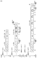
- FIG. It is a figure for demonstrating the processing of the communication frame by the relay device according to Embodiment 2.
- FIG. It is a figure for demonstrating the data aggregation process according to Embodiment 2.
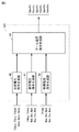
- FIG. It is a figure for demonstrating an example of the processing of the communication frame by the submodule 7 according to Embodiment 3.
- FIG. It is a figure for demonstrating another example of processing of a communication frame by a submodule 7 according to Embodiment 3.
- FIG. It is a figure for demonstrating the transmission method of the command information according to Embodiment 4.
- FIG. 1 is a schematic configuration diagram of a power conversion device.
- the power converter 1 is composed of a modular multi-level converter including a plurality of sub modules (corresponding to “SM” in FIG. 1) 7 connected in series with each other. ..
- the "submodule” is also referred to as a "converter cell” or "unit converter”.
- the power conversion device 1 performs power conversion between the DC circuit 14 and the AC circuit 12.
- the power conversion device 1 includes a power conversion circuit unit 2 and a command generation device 3.
- the power conversion circuit unit 2 includes a plurality of leg circuits 4u connected in parallel between the positive electrode DC terminal (that is, the high potential side DC terminal) Np and the negative electrode DC terminal (that is, the low potential side DC terminal) Nn. , 4v, 4w (hereinafter, also collectively referred to as "leg circuit 4").
- the leg circuit 4 is provided in each of the plurality of phases constituting the alternating current.
- the leg circuit 4 is connected between the AC circuit 12 and the DC circuit 14, and performs power conversion between the two circuits.
- FIG. 1 shows a case where the AC circuit 12 is a three-phase AC system, and three leg circuits 4u, 4v, and 4w are provided corresponding to the U phase, the V phase, and the W phase, respectively.
- the AC input terminals Nu, Nv, Nw provided in the leg circuits 4u, 4v, 4w, respectively, are connected to the AC circuit 12 via the interconnection transformer 13.
- the AC circuit 12 is, for example, an AC power system including an AC power supply and the like.
- FIG. 1 the connection between the AC input terminals Nv, Nw and the interconnection transformer 13 is not shown for ease of illustration.
- the high-potential side DC terminal Np and the low-potential side DC terminal Nn commonly connected to each leg circuit 4 are connected to the DC circuit 14.
- the DC circuit 14 is, for example, a DC terminal of a DC power system or other power conversion device including a DC transmission network or the like.
- the interconnection transformer 13 of FIG. 1 may be configured to be connected to the AC circuit 12 via an interconnection reactor.
- the leg circuits 4u, 4v, 4w are provided with primary windings, respectively, and the leg circuits 4u, 4v, 4w are provided via the secondary windings magnetically coupled to the primary windings. May be connected to the interconnection transformer 13 or the interconnection reactor in an alternating current manner.
- the primary winding may be the following reactors 8A and 8B.
- leg circuit 4 is electrically (that is, DC or AC) through the connection portion provided in each leg circuit 4u, 4v, 4w such as the AC input terminals Nu, Nv, Nw or the above-mentioned primary winding. It is connected to the AC circuit 12.
- the leg circuit 4u includes an upper arm 5 from the high potential side DC terminal Np to the AC input terminal Nu, and a lower arm 6 from the low potential side DC terminal Nn to the AC input terminal Nu.
- the AC input terminal Nu which is the connection point between the upper arm 5 and the lower arm 6, is connected to the interconnection transformer 13.
- the high potential side DC terminal Np and the low potential side DC terminal Nn are connected to the DC circuit 14. Since the leg circuits 4v and 4w have the same configuration, the leg circuits 4u will be described below as a representative.
- the upper arm 5 includes a plurality of cascade-connected submodules 7 and a reactor 8A.
- the plurality of submodules 7 and the reactor 8A are connected in series with each other.
- the lower arm 6 includes a plurality of cascaded submodules 7 and a reactor 8B.
- the plurality of submodules 7 and the reactor 8B are connected in series with each other.
- the position where the reactor 8A is inserted may be any position of the upper arm 5 of the leg circuit 4u, and the position where the reactor 8B is inserted may be any position of the lower arm 6 of the leg circuit 4u. Good.
- the inductance values of each reactor may be different from each other. Only the reactor 8A of the upper arm 5 or only the reactor 8B of the lower arm 6 may be provided.
- Reactors 8A and 8B are provided so that the accident current does not suddenly increase in the event of an accident such as an AC circuit 12 or a DC circuit 14.
- the inductance values of the reactors 8A and 8B are made excessive, there arises a problem that the efficiency of the power converter is lowered. Therefore, in the event of an accident, it is preferable to stop (that is, turn off) all the switching elements of each submodule 7 in the shortest possible time.
- the power conversion device 1 includes an AC voltage detector 10, an AC current detector 16, and DC voltage detectors 11A and 11B as each detector for measuring the amount of electricity (for example, current, voltage, etc.) used for control. And arm current detectors 9A and 9B provided in each leg circuit 4.
- the signals detected by these detectors are input to the command generator 3.
- the command generator 3 outputs operation commands 15pu, 15nu, 15pv, 15nv, 15pw, and 15nw for controlling the operation state of each submodule 7 based on these detection signals. Further, the command generator 3 receives information 17 from each submodule 7.
- the information 17 is internal information of the sub-module 7, and includes a voltage value of the capacitor 24 of the sub-module 7, state information indicating the state of the sub-module 7, and the like.
- the operation commands 15pu, 15nu, 15pv, 15nv, 15pw, 15nw are U-phase upper arm, U-phase lower arm, V-phase upper arm, V-phase lower arm, W-phase upper arm, and W-phase. It is generated corresponding to each lower arm.
- the operation command 15pu, 15nu, 15pv, 15nv, 15pw, 15nw will be referred to as the operation command 15 when they are generically or arbitrarily indicated.
- the AC voltage detector 10 detects the U-phase AC voltage value Vacu, the V-phase AC voltage value Vacv, and the W-phase AC voltage value Vacw of the AC circuit 12.
- the AC current detector 16 detects the U-phase AC current value Iacu, the V-phase AC current value Iacv, and the W-phase AC current value Iacw of the AC circuit 12.
- the DC voltage detector 11A detects the DC voltage value Vdcp of the high potential side DC terminal Np connected to the DC circuit 14.
- the DC voltage detector 11B detects the DC voltage value Vdcn of the low potential side DC terminal Nn connected to the DC circuit 14.
- the arm current detectors 9A and 9B provided in the leg circuit 4u for the U phase detect the upper arm current Ipu flowing through the upper arm 5 and the lower arm current Inu flowing through the lower arm 6, respectively.
- the arm current detectors 9A and 9B provided in the V-phase leg circuit 4v detect the upper arm current Ipv and the lower arm current Inv, respectively.
- the arm current detectors 9A and 9B provided in the leg circuit 4w for the W phase detect the upper arm current Ipw and the lower arm current Inw, respectively.
- FIG. 2 is a circuit diagram showing an example of submodules constituting each leg circuit of FIG.
- the submodule 7 includes a half-bridge type conversion circuit 25, a capacitor 24 as an energy storage device, a gate control unit 21, a voltage detection unit 27, and a transmission / reception unit 28.
- the gate control unit 21, the voltage detection unit 27, and the transmission / reception unit 28 may be configured by a dedicated circuit, or may be configured by using an FPGA (Field Programmable Gate Array) or the like.
- FPGA Field Programmable Gate Array
- the conversion circuit 25 includes switching elements 22A and 22B connected in series with each other and diodes 23A and 23B.
- the diodes 23A and 23B are connected to the switching elements 22A and 22B in antiparallel (that is, in parallel and in the antibias direction), respectively.
- the capacitor 24 is connected in parallel with the series connection circuit of the switching elements 22A and 22B, and holds a DC voltage.
- the connection nodes of the switching elements 22A and 22B are connected to the input / output terminals 26P on the high potential side.
- the connection node between the switching element 22B and the capacitor 24 is connected to the input / output terminal 26N on the low potential side.
- the gate control unit 21 operates in accordance with the operation command 15 received from the command generator 3 of FIG. During normal operation (that is, when a zero voltage or a positive voltage is output between the input / output terminals 26P and 26N), the gate control unit 21 turns one of the switching elements 22A and 22B on and the other off. Control so that When the switching element 22A is in the ON state and the switching element 22B is in the OFF state, a voltage between both ends of the capacitor 24 is applied between the input / output terminals 26P and 26N. When the switching element 22A is in the off state and the switching element 22B is in the on state, the voltage between the input / output terminals 26P and 26N is 0V.
- the sub-module 7 outputs a zero voltage or a positive voltage depending on the voltage of the capacitor 24 by alternately turning on the switching elements 22A and 22B.
- the voltage detection unit 27 detects the voltage between 24P and 24N across the capacitor 24.
- the transmission / reception unit 28 transmits the operation command 15 received from the command generator 3 of FIG. 1 to the gate control unit 21, and the voltage of the capacitor 24 detected by the voltage detection unit 27 (hereinafter, also simply referred to as “capacitor voltage”).
- Information 17 including.) Is transmitted to the command generator 3.
- each switching element 22A and 22B a self-extinguishing type switching element capable of controlling both on operation and off operation is used.
- the switching elements 22A and 22B are, for example, an IGBT (Insulated Gate Bipolar Transistor) or a GCT (Gate Commutated Turn-off thyristor).
- the configuration of the submodule 7 described above is an example, and submodules 7 having other configurations may be applied to the present embodiment.
- the sub-module 7 may be configured by using a full-bridge type conversion circuit or a three-quarter bridge type conversion circuit.
- FIG. 3 is a block diagram showing a schematic configuration of the command generator.
- the command generation device 3 includes a control device 101, a protection device 102, and a relay device group 320 composed of a plurality of relay devices.
- Each of the control device 101 and the protection device 102 corresponds to a higher-level device of each relay device included in the relay device group 320.
- Each relay device relays communication between the host device and each submodule 7 included in the power conversion circuit unit 2.
- FIG. 3 only the U-phase leg circuit 4u of the power conversion circuit unit 2 of FIG. 1 is typically shown, but the same applies to the other leg circuits 4v and 4w.
- the control device 101 is a device that controls the operation of each submodule 7.
- the control device 101 includes AC voltage values Vac, Vacv, Vacw (hereinafter, also collectively referred to as “AC voltage value Vac”) and AC current values Iacu, Iacv, Iacw (hereinafter, ““ AC voltage value Vac ”) detected by each detector in FIG.
- AC current value Iac AC current value
- DC voltage values Vdcp, Vdcn upper arm currents Ipu, Ipv, Ipw
- lower arm currents Inu, Inv, Inw hereinafter, it is also collectively referred to as “lower arm current In”
- receives inputs of the capacitor voltage Vcap receives inputs of the capacitor voltage Vcap.
- the capacitor voltage Vcap is the average of the voltage values of the capacitors 24 detected in each submodule 7 for each arm circuit.
- the control device 101 generates a control command for operating and controlling each submodule 7 in a normal operation control period for each period T1 (for example, 86.8 ⁇ s) based on each received detection value.
- the generated control command is output to the relay device group 320.
- Control commands include voltage commands, current commands, etc.
- the voltage command is, for example, the output voltage command value of the upper arm 5 and the output voltage command value of the lower arm 6 in each of the leg circuits 4u, 4v, 4w.
- the current command is, for example, the output current command value of the upper arm 5 and the output current command value of the lower arm 6 in each of the leg circuits 4u, 4v, 4w.
- the control device 101 typically includes an auxiliary transformer, an AD (Analog to Digital) conversion unit, a calculation unit, and the like as a hardware configuration.
- the arithmetic unit includes a CPU (Central Processing Unit), a RAM (Random Access Memory), and a ROM (Read Only Memory).
- the AD conversion unit includes an analog filter, a sample hold circuit, a multiplexer, and the like.
- the control device 101 may be composed of, for example, a digital protection control device.
- the protection device 102 is a device that protects each sub-module 7. When at least one of the arm currents exceeds the threshold value, the protection device 102 generates a protection command including a stop command for stopping the operation of each submodule 7, and sends the protection command to each relay device 32. Send to. On the other hand, the protection device 102 does not generate a protection command when all the arm currents are less than the threshold value, or generates a protection command including a normal command for operating each submodule 7 based on the control command. You may. The protection device 102 transmits a protection command every cycle T2 (for example, several ⁇ s).
- the relay device group 320 receives a control command from the control device 101 and receives a protection command from the protection device 102.
- the relay device group 320 outputs an operation command 15 including at least one of a control command and a protection command to each submodule 7.
- Each submodule 7 operates according to the operation command 15.
- FIG. 4 is a diagram for explaining a method of transmitting command information according to the first embodiment.
- the method of transmitting the control command from the control device 101 to the relay device group 320 and the method of transmitting the protection command from the protection device 102 to the relay device group 320 are the same. Therefore, in the following description, it is assumed that the host device is the control device 101. This also applies to other embodiments.
- the control device 101 includes a command information generation unit 151 and a plurality of communication control units 153A and 153B (hereinafter, also collectively referred to as “communication control unit 153”). Each of these functions is realized, for example, by the CPU of the control device 101 executing a program stored in the ROM. Some or all of these functions may be configured to be realized by using a dedicated circuit.
- the command information generation unit 151 generates command information 90 including arm commands for each arm (that is, the upper and lower arms of each phase) included in the power conversion circuit unit 2.
- the command information 90 corresponds to the control command.
- the command information 90 includes a common command common to each arm (that is, the upper and lower arms of each phase) included in the power conversion circuit unit 2, and an arm command dedicated to the upper and lower arms of each phase.
- each arm command is an arm command U_u for the upper arm 5 of the U phase, an arm command U_d for the lower arm 6 of the U phase, an arm command V_u for the upper arm 5 of the V phase, and a lower V phase. It includes an arm command V_d for the arm 6, an arm command W_u for the upper arm 5 of the W phase, and an arm command W_d for the lower arm 6 of the W phase.
- the common command includes a mode command that specifies the operation mode of each submodule 7 and the total number of each submodule 7 included in the power conversion circuit unit 2.
- the operation mode includes an activation mode for activating the submodule 7, an operation mode for normal operation of the submodule 7, and a pause mode for temporarily stopping the submodule 7.
- Each arm command includes an arm voltage command value, an arm current command value, and an arm test command.
- the arm test command includes a command to start test charging of the capacitor 24 of the sub-module 7 in the arm and a command to stop test charging.
- FIG. 5 is a diagram for explaining an example of an arm voltage command generation method.
- the command information generation unit 151 of the control device 101 has an AC voltage command generation unit 40, a DC voltage command generation unit 41, and a circulating current command generation as a functional configuration for generating an arm voltage command.
- a unit 42 and an arm voltage command generation unit 44 are included.
- Each of these functional units is composed of, for example, a feedback controller such as a PID controller (Proportional-Integral-Differential Controller).
- PID controller Proportional-Integral-Differential Controller
- the AC voltage command generation unit 40 generates AC voltage command values for each phase based on the AC voltage values Vaku, Vacv, and Vacw and the AC current values Iac, Iacv, and Iacw.
- the DC voltage command generation unit 41 calculates the DC current value Idc based on the upper arm currents Ipu, Ipv, Ipw and the lower arm currents Inu, Inv, Inw.
- the DC voltage command generation unit 41 generates a DC voltage command value based on the DC voltage values Vdcp and Vdcn and the DC current value Idc.
- the circulation current command generation unit 42 calculates the circulation currents Iccu, Iccv, and Iccw flowing in the leg circuits 4u, 4v, and 4w, respectively, based on the upper arm currents Ipu, Ipv, Ipw and the lower arm currents Inu, Inv, and Inw of each phase. To do.
- the circulating current is a current that circulates between the plurality of leg circuits 4.
- the circulating current command generation unit 42 calculates the command value of the circulating current of each phase based on the circulating currents Iccu, Iccv, and Iccw of each phase and the capacitor voltage Vcap averaged for each arm circuit.
- the arm voltage command generation unit 44 generates arm voltage commands Vprefu, Vnrefu, Vprefv, Vnrefv, Vprefw, Vnrefw for the upper arm 5 and the lower arm 6 of each phase by synthesizing each of the above command generation units.
- the command information generation unit 151 broadcasts the command information 90 to the communication control unit 153 corresponding to each arm.
- the communication control unit 153 is provided corresponding to each arm. In FIG. 4, for simplification of the illustration, only the communication control unit 153A corresponding to the U-phase upper arm 5 and the communication control unit 153B corresponding to the U-phase lower arm 6 are shown, but they are actually shown.
- the control device 101 further includes two communication control units 153 for the V-phase upper and lower arms and two communication control units 153 for the W-phase upper and lower arms. Since the functions of the communication control units 153 corresponding to each arm are the same, the functions of the communication control units 153A and 153B for the U phase will be described here.
- the communication control unit 153A receives the command information 90 transmitted from the command information generation unit 151, and extracts the arm command U_u corresponding to the communication control unit 153A from the command information 90.
- the communication control unit 153A transmits a communication frame 51A including the extracted arm command U_u to each relay device 32 connected to each submodule 7 in the U phase upper arm corresponding to the communication control unit 153A.
- the communication control unit 153A includes a selector 31A, a communication frame generation unit 52A, and a plurality of communication ports 34A.
- the selector 31A selects the arm command U_u corresponding to the selection ID “Uu” set in itself and outputs it to the communication frame generation unit 52A.
- the slot number on which the board is mounted is set as the selection ID.
- the selection ID "Uu” is automatically set in the selector 31A of the communication control unit 153A. According to this, it is not necessary to manually set the communication control unit 153, which is expected to have effects such as labor saving of initial setting work and prevention of number setting error.
- the function of the selector 31A may be implemented by software.
- the communication frame generation unit 52A extracts a common command from the command information 90, and extracts the arm command U_u selected by the selector 31A.
- the communication frame generation unit 52A generates a communication frame 51A including command data having a common command and an arm command U_u.
- the communication frame generation unit 52A transmits the communication frame 51A to each relay device 32 via each communication port 34A.
- N communication ports 34A (however, an integer of N ⁇ 1) are provided. For convenience, numbers # 1 to # N are assigned to the N communication ports 34A to distinguish them.
- the communication frame generation unit 52A simultaneously transmits the communication frame 51A to each communication port 34A # 1 to 34A # N.
- Each communication port 34A # 1 to 34A # N transmits a communication frame 51A to each relay device 32.
- Each communication control unit 153 is connected to a plurality of relay devices 32 via a ring-type network.
- four relay devices 32 are connected to each communication port 34 of the communication control unit 153 by a ring-type network.
- the four relay devices 32 are also referred to as HUBs # 1 to # 4, respectively.
- Each relay device 32 is connected to a predetermined number of submodules 7 via a star-shaped network. Each relay device 32 takes out the command data included in the communication frame 51A, and transmits the communication frame including the command data to each sub-module 7 connected to the relay device 32.
- a network between the control device 101, each relay device 32, and each submodule 7 is constructed by combining the ring-type network topology and the star-type network topology.
- the communication control unit 153B receives the command information 90 transmitted from the command information generation unit 151, and extracts the arm command U_d corresponding to the communication control unit 153B from the command information 90.
- the communication control unit 153B transmits the communication frame 51B including the extracted arm command U_d to each relay device 32 connected to each sub-module 7 in the U-phase lower arm corresponding to the communication control unit 153B.
- the communication control unit 153B includes a selector 31B, a communication frame generation unit 52B, and a plurality of communication ports 34B.
- the selector 31B selects the arm command U_d corresponding to the selection ID “Ud” set in itself and outputs it to the communication frame generation unit 52B.
- the communication frame generation unit 52B generates a communication frame 51B including a common command and an arm command U_d, and transmits the communication frame 51B to each relay device 32 via each communication port 34B.
- Each communication port 34B is connected to each relay device 32 by a ring-type network, but the connection relationship is not shown for the sake of facilitation of illustration.
- the corresponding communication frame is also transmitted to each relay device 32 from the communication control unit 153 for the upper and lower arms of the V phase and the communication control unit 153 for the upper and lower arms of the W phase.
- each of the plurality of communication control units 153 is included in the arm corresponding to the communication control unit 153 (for example, the U-phase upper arm).
- a communication frame (for example, communication frame 51A) including an arm command (for example, arm command U_u) for the arm is transmitted to the relay device 32 connected to each sub-module 7.
- the communication frame is transmitted for each arm, it is not necessary to provide information for designating the arm in the communication frame. Therefore, since the control device 101 can simultaneously transmit the corresponding arm command to the sub-module 7 in each arm, the communication time required for command transmission from the control device 101 can be shortened.
- FIG. 4 describes a case where the host device is the control device 101.
- the command information 90 corresponds to the protection command.
- the common command of the command information 90 includes a stop command for stopping the operation of the submodules 7 of all the arms.
- Each of the 80 arm commands in the command information includes a stop command to stop the operation of each submodule 7 in the corresponding arm.
- the arm command U_u generated by the command information generation unit of the protection device 102 includes a stop command for stopping the operation of each submodule 7 in the U-phase upper arm.
- FIG. 6 is a diagram showing an example of a network configuration according to the first embodiment. Specifically, FIG. 6 shows a network configuration when the number of communication ports N in FIG. 4 is one.
- the control device 101 includes a communication port 34A for the U-phase upper arm, a communication port 34B for the U-phase lower arm, a communication port 34C for the V-phase upper arm, and a V-phase lower arm.
- the communication port 34D, the communication port 34E for the W phase upper arm, and the communication port 34F for the W phase lower arm are included.
- the communication port 34A is ring-connected to the four relay devices 32. Each relay device 32 is star-connected to a plurality of submodules 7.
- the communication frame 51A output from the communication port 34A is transmitted in the order of the numbers (1), (2), (3), (4), and (5) in parentheses in FIG.
- the transmission method of the communication frame output from each communication port 34B to 34F is the same as the transmission method of the communication frame output from the communication port 34A.
- the control device 101 transmits the communication frame 51A to the HUB # 1 via the communication port 34A.
- HUB # 1 processes the communication frame 51A received from the control device 101 and transmits it to HUB # 2.
- HUB # 2 processes the communication frame 51A received from HUB # 1 and transmits it to HUB # 3.
- HUB # 3 processes the communication frame 51A received from HUB # 2 and transmits it to HUB # 4.
- HUB # 4 processes the communication frame 51A received from HUB # 3 and transmits it to the control device 101.
- the processing content of the communication frame 51A will be described later.
- FIG. 7 is a diagram showing another example of the network configuration according to the first embodiment. Specifically, FIG. 7 shows a network configuration when the number of communication ports N in FIG. 4 is two. With reference to FIG. 7, the control device 101 has two communication ports 34A, two communication ports 34B, two communication ports 34C, two communication ports 34D, two communication ports 34E, and two communications. Includes port 34F.
- Each of the two communication ports 34A is ring-connected to the four relay devices 32.
- Each relay device 32 is star-connected to a plurality of submodules 7.
- the communication frame 51A output from each communication port 34A transmits the numbers (1), (2), (3), (4), and (5) in parentheses in FIG. 7 in this order, as in the case of FIG. Will be done.
- FIG. 8 is a diagram for explaining an example of processing a communication frame by the relay device according to the first embodiment.
- the processing of each communication frame transmitted through each communication port of the control device 101 is the same. Therefore, a processing example of the communication frame 51A transmitted from the control device 101 via the communication port 34A will be described.
- the numbers (1), (2), (3), (4), and (5) in parentheses in FIG. 7 correspond to the numbers in parentheses in FIG.
- the communication frame 51A transmitted from the control device 101 to HUB # 1 is changed to "communication frame 51A_1"
- the communication frame 51A transmitted from HUB # 1 to HUB # 2 is changed to "communication frame 51A_2”
- HUB # 2 to HUB # 3.
- the transmitted communication frame 51A is referred to as "communication frame 51A_3”
- the communication frame 51A transmitted from HUB # 3 to HUB # 4 is referred to as "communication frame 51A_4"
- the communication frame 51A transmitted from HUB # 4 to the control device 101 is referred to as "communication frame 51A_3”.
- the communication frame 51A_1 has a flag area 81 (corresponding to “flg” in the figure), a header area 82, a payload area 83, and an FCS (Frame Check Sequence) in which error detection information is stored. Includes region 84.
- Information such as a communication command (corresponding to "cmd” in the figure), a sequence number (corresponding to "seq” in the figure), and a payload length (corresponding to "pl” in the figure) is stored in the header area 82.
- Command data X including a common command and an arm command U_u is stored in the payload area 83.
- the HUB # 1 When the HUB # 1 receives the communication frame 51A_1 from the communication control unit 153A connected to itself, the HUB # 1 processes the communication frame 51A_1 to generate the communication frame 51A_2. Specifically, HUB # 1 generates the communication frame 51A_2 by adding the HUB data Y1 to the payload area of the communication frame 51A_1 and updating the payload length and the FCS area 84. HUB # 1 transmits the communication frame 51A_2 to HUB # 2 connected to HUB # 1.
- HUB # 1 generates HUB data Y1 based on the internal information (hereinafter, also referred to as "SM internal information") received from each submodule 7 connected to the HUB # 1.
- the HUB data Y1 includes SM internal information received from each submodule 7 and the state information of HUB # 1 (corresponding to the “HUB state” in the figure).
- the SM internal information includes the capacitor voltage of each submodule 7 (corresponding to "SM # 1 voltage to SM # N voltage” in the figure) and the state information of each submodule 7 ("SM # 1 state to SM" in the figure. Corresponds to "#N state”) and is included.
- the capacitor voltage of the sub-module 7 is also referred to as “SM voltage”
- the state information of the sub-module 7 is also referred to as “state information Dsm”
- state information of the HUB is also referred to as “state information Dh”.
- the status information Dsm includes operation information indicating the operating status of the submodule 7, failure rank information indicating the degree of failure, and failure type information indicating the type of failure.
- the operation information of the sub-module 7 includes a start-up bit indicating whether or not it is starting up, a failure bit indicating whether or not it is in failure, and a separation bit dependent on the failure bit indicating the failure state.
- the separation bit is information indicating whether or not the failed submodule 7 has been separated from the arm.
- the failure rank information includes information indicating whether or not the submodule 7 can be operated.
- the operation information may include a control bit indicating whether or not the operation is being controlled, and a stop bit indicating whether or not the operation is being stopped.
- the state information Dh of HUB # 1 includes operation information indicating the operating state of HUB # 1, failure rank information indicating the degree of failure of HUB # 1, and failure type information indicating the type of failure.
- the operation information of HUB # 1 includes an operation bit indicating whether it is in normal operation or in failure.
- the failure rank information includes information indicating whether or not HUB # 1 can be operated.
- HUB # 2 adds HUB data Y2 to the communication frame 51A_2, updates the payload length and the FCS area 84, and generates the communication frame 51A_3.
- HUB # 3 adds HUB data Y3 to the communication frame 51A_3, updates the payload length and the FCS area 84, and generates the communication frame 51A_4.
- the HUB # 4 adds the HUB data Y4 to the communication frame 51A_4 received from the HUB # 3 connected to itself, updates the payload length and the FCS area 84, and generates the communication frame 51A_5.
- HUB # 4 transmits the communication frame 51A_5 to the control device 101.
- the HUB data Y2 includes SM internal information received from each submodule 7 connected to the HUB # 2 and the state information of the HUB # 2. The same applies to the HUB data Y3 and Y4. As a result, as shown in FIG. 8, the command data X and the HUB data Y1 to Y4 are stored in the payload area 83 of the communication frame 51A_5. In this way, the communication frame transmitted from the control device 101 is concatenated with a field of HUB data each time it passes through the HUB. Therefore, the communication frames 51A_1 to 51A_5 have different formats.
- the command data X is transmitted to each relay device 32 for the U phase upper arm, and the HUB data of each relay device 32 is transmitted. Acquisition of Y1 to Y4 is performed.
- command data can be transmitted to each relay device 32 for other arms and HUB data of each relay device 32 can be acquired. It is done.
- the transmission of the command data to all the relay devices 32 connected to the control device 101 and the acquisition of the HUB data of all the relay devices 32 are performed at the same time. Therefore, according to the present embodiment, the communication frequency can be reduced and the communication time can be shortened as compared with the method in which the identification numbers of the relay device 32 and the sub-module 7 are designated and individually communicated. Further, the communication frame is automatically expanded according to the number of relay devices 32. For example, even when one relay device 32 is added later, it is not necessary to change the configuration of the communication frame transmitted from the control device 101.
- FIG. 8 describes the case where the host device is the control device 101.
- the SM internal information includes the state information Dsm and does not include the SM voltage.
- the HUB data includes the state information Dsm and the state information Dh. The other points are the same.
- the command data is transmitted from the higher-level device to the relay device 32 and the HUB data of the relay device 32 is acquired at the same time. Therefore, the communication frequency between the host device and the relay device 32 can be reduced and the communication time can be shortened. Further, since the communication frame is automatically expanded according to the number of relay devices 32, it is not necessary to change the configuration of the communication frame even when the relay device 32 is added later.
- Embodiment 2 In the first embodiment, a configuration in which HUB data is added to the communication frame when passing through each HUB has been described. In the second embodiment, a configuration will be described in which aggregated data that has been subjected to data aggregation processing when passing through each HUB is added to the communication frame.
- FIG. 9 is a diagram for explaining the processing of the communication frame by the relay device according to the second embodiment.
- the numbers (1), (2), (3), (4), and (5) in parentheses in FIG. 9 correspond to the numbers in parentheses in FIG.
- the communication frame 51A_a1 transmitted from the control device 101 to the HUB # 1 is the same as the communication frame 51A_1 in FIG.
- the communication frame 51A_a2 transmitted from the HUB # 1 to the HUB # 2 is different from the communication frame 51A_2 in FIG. 8 in the content of the payload area 83.
- HUB # 1 generates HUB aggregate data Z1 and HUB data Y1a based on SM internal information received from each submodule 7 connected to HUB # 1.
- HUB # 1 adds HUB aggregate data Z1 and HUB data Y1a to the payload area 83 of the communication frame 51A_a1, updates the payload length and the FCS area 84, and generates the communication frame 51A_a2.
- the payload area 83 of the communication frame 51A_a2 includes the command data X, the HUB aggregate data Z1, and the HUB data Y1a.
- the HUB aggregated data Z1 includes an aggregated value of SM voltage, an aggregated value of state information Dsm, and an aggregated value of state information Dh.
- the HUB data Y1a includes a part of the state information Dsm of the submodule 7 connected to the HUB # 1 and the state information Dh of the HUB # 1. The contents of the HUB aggregate data Z1 and the HUB data Y1a will be described later.
- HUB # 2 adds HUB data Y2a to the communication frame 51A_a2 and generates HUB aggregated data Z2 which is an updated version of HUB aggregated data Z1. Further, HUB # 2 updates the payload length and the FCS area 84 to generate the communication frame 51A_3a.
- FIG. 10 is a diagram for explaining the data aggregation process according to the second embodiment.
- HUB # 2 executes data aggregation processing using the SM internal information of each submodule 7 connected to itself, and generates HUB aggregation data Z1.
- the SM voltage aggregated value 301 in the HUB aggregated data Z1 is an added value of each SM voltage received from each submodule 7 connected to the HUB # 1.
- the aggregated value of the state information Dsm in the HUB aggregated data Z1 includes the activation bit aggregation value 303, the activation SM number aggregation value 305, and the failure bit aggregation value 307.
- the activation bit aggregation value 303 is the logical product of each activation bit received from each submodule 7. For example, if all the submodules 7 connected to HUB # 1 are activated, the logical product is "1", and if at least one submodule 7 is not activated, the logical product is "0". It becomes. From the value of the logical product, it can be determined whether or not all the submodules 7 connected to HUB # 1 are activated.
- the activation SM number aggregate value 305 is an addition value of each activation bit received from each submodule 7. This added value corresponds to the number of submodules 7 that have been activated among the submodules 7 connected to HUB # 1.
- the failure bit aggregation value 307 is the logical sum of each failure bit received from each submodule 7. For example, if all the submodules 7 connected to HUB # 1 are not failed, the logical sum is "0", and if at least one submodule 7 is failed, the logical sum is "1". It becomes. From the value of the logical sum, it can be determined whether or not the failed submodule 7 exists in each submodule 7 connected to HUB # 1.
- the HUB data Y1a includes a part of the state information Dsm and the state information Dh. Specifically, the HUB data Y1a includes a failure bit, a separation bit, a failure rank information, and a failure type information in the state information Dsm of each submodule 7, and a state information Dh of HUB # 1. As described above, since the HUB data Y1a does not include the SM voltage and the start bit of the sub-module 7, the HUB data Y1a has a smaller data size than the HUB data Y1 in FIG.
- HUB # 2 updates the HUB aggregated data Z1 to generate the HUB aggregated data Z2.
- the HUB aggregated data Z2 includes the SM voltage aggregated value 301F with the SM voltage aggregated value 301 updated, the activated bit aggregated value 303F with the activated bit aggregated value 303 updated, and the activated SM number aggregated value with the activated SM number aggregated value 305 updated.
- 305F and the failure bit aggregation value 307F which updated the failure bit aggregation value 307 are included.
- the SM voltage aggregate value 301F is the sum of the SM voltage aggregate value 301 and each SM voltage received by the HUB # 2.
- the activation bit aggregation value 303F is a logical product of the activation bit aggregation value 303 and each activation bit received by HUB # 2.
- the activation SM number aggregation value 305F is an addition value of the activation SM number aggregation value 305 and each activation bit received by HUB # 2.
- the failure bit aggregation value 307F is the logical sum of the failure bit aggregation value 307 and each failure bit received by HUB # 2.
- the HUB data Y2a includes a failure bit, a separation bit, a failure rank information, and a failure type information in each state information Dsm received by the HUB # 2, and a state information Dh of the HUB # 2. Since the HUB data Y2a contains only a part of the state information Dsm, the HUB data Y2a has a smaller data size than the HUB data Y2 in FIG.
- the aggregated value of the state information Dh in the HUB aggregated data Z1 is the operating bit of the HUB # 1. Further, the aggregated value of the state information Dh in the HUB aggregated data Z2 is a logical product of the operating bits of HUB # 1 and the operating bits of HUB # 2.
- HUB # 3 performs aggregation processing on the HUB aggregated data Z2 of the communication frame 51A_a3, updates it to the HUB aggregated data Z3, adds the HUB data Y3a, and adds the payload length and the FCS area 84. It is updated to generate the communication frame 51A_a4.
- HUB # 4 performs aggregation processing on the HUB aggregated data Z3 and updates it to the HUB aggregated data Z4, adds the HUB data Y4a to the communication frame 51A_a4, updates the payload length and the FCS area 84, and updates the communication frame 51A_a5.
- HUB # 4 transmits the communication frame 51A_a5 to the control device 101.
- the data size of the HUB data Y1a to Y4a in which the individual data of the submodule 7 is stored can be made smaller than the data size of the HUB data Y1 to Y4 in FIG. 8, respectively. That is, the frame lengths of the communication frames 51A_a2 to 51A_a5 can be made shorter than the frame lengths of the communication frames 51A_2 to 51A_5 in FIG. 8, respectively.
- the time required for one communication can be shortened.
- the amount of memory and the amount of calculation required by the control device 101 or the protection device 102 can be reduced.
- it is possible to configure a communication path with a low-speed and inexpensive communication module for example, a communication module of 1 to 2 Gbps class. Further, since the communication time can be shortened even when a large number of submodules 7 are connected, it becomes easy to construct a large-scale HDVC system.
- Embodiment 3 In the first embodiment, the configuration in which the relay device 32 is connected to each sub-module 7 via a star-type network has been described, but in the third embodiment, the relay device 32 is connected to each sub module via a ring-type network. The configuration connected to the module 7 will be described.
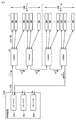
- FIG. 11 is a diagram showing a network configuration according to the third embodiment.
- the network configuration of FIG. 11 corresponds to a configuration in which the connection form of the relay device 32 and each submodule 7 in FIG. 6 is changed to a ring type.
- each communication port 351 to 354 of each relay device 32 is ring-connected to a plurality of submodules 7.
- numbers # 1 to # 16 are assigned to each submodule to distinguish them from each other.
- the 16 submodules 7 are also referred to as submodules # 1 to # 16, respectively.
- the communication port 351 of HUB # 1 is ring-connected to the sub-modules # 1 to # 4, the communication port 352 is ring-connected to the sub-modules # 5 to # 8, and the communication port 353 is ring-connected to the sub-modules # 9 to # 12.
- the communication port 354 is ring-connected to the submodules # 13 to # 16.
- the communication frame output from the communication port 351 is transmitted in the order of the numbers (1), (2), (3), (4), and (5) in parentheses in FIG. The same applies to HUB # 2 to # 4.
- FIG. 12 is a diagram for explaining an example of processing of a communication frame by the submodule 7 according to the third embodiment.
- the processing of the communication frame described with reference to FIG. 12 is basically the same as the processing of the communication frame described with reference to FIG. Further, the processing of each communication frame transmitted via each communication port of the relay device 32 is the same. Therefore, here, a processing example of a communication frame transmitted from the communication port 351 will be described.
- the numbers (1), (2), (3), (4), and (5) in parentheses in FIG. 12 correspond to the numbers in parentheses in FIG.
- the communication frame 61_1 transmitted from the HUB # 1 to the submodule # 1 includes a flag area 86, a header area 87, a payload area 88, and an FCS area 89.
- the header area 87 includes information such as a communication command, a sequence number, and a payload length.
- the payload area 88 includes command data X having a common command and an arm command U_u.
- Submodule # 1 adds SM data K1 to the payload area of the communication frame 61_1 received from HUB # 1 and updates the payload length and the FCS area 89 to generate the communication frame 61_2.
- the SM data K1 includes SM internal information of the sub-module # 1.
- the SM internal information includes the capacitor voltage of the submodule # 1 and the state information Dsm.
- the sub-module # 2 generates the communication frame 61_3
- the sub-module # 3 generates the communication frame 61_4
- the sub-module # 4 generates the communication frame 61_5.
- Command data X and SM data K1 to K4 are stored in the payload area 88 of the communication frame 61_5.
- the SM data K2 to K4 include SM internal information of the submodules # 2 to # 4, respectively.
- the SM data field is linked to the communication frame transmitted from the relay device 32 each time it passes through each submodule 7. Therefore, the communication frames 61_1 to 61_5 have different formats.
- FIG. 13 is a diagram for explaining another example of processing a communication frame by the submodule 7 according to the third embodiment.
- the processing of the communication frame described with reference to FIG. 13 is basically the same as the processing of the communication frame described with reference to FIG.
- a processing example of a communication frame transmitted from the communication port 351 will be described.
- the communication frame 63_1 transmitted from the HUB # 1 to the submodule # 1 is the same as the communication frame 61_1 in FIG.
- the communication frame 63_2 transmitted from the sub-module # 1 to the sub-module # 2 is different from the communication frame 61_2 in FIG. 12 in the contents of the payload area 88.
- the payload area 88 of the communication frame 63_2 includes the command data X, the SM aggregate data Zs1, and the SM data K1a.
- the SM aggregated data Zs1 is the aggregated value of the SM voltage of the submodule # 1 and the aggregated value of the state information Dsm of the submodule # 1 (for example, the aggregated value of the startup bits, the aggregated value of the number of activated SMs, and the aggregated value of the failed bits). And include.
- the aggregated value of the SM voltage of the sub-module # 1 is the SM voltage of the sub-module # 1.
- the start bit aggregate value and the start SM number aggregate value are start bits of submodule # 1.
- the fault bit aggregate value is the fault bit of submodule # 1.
- the SM data K1a includes a failure bit, a separation bit, a failure rank information, and a failure type information of the submodule # 1. Since the SM data K1a contains only a part of the state information Dsm, the SM data K1a has a smaller data size than the SM data K1 in FIG.
- Submodule # 2 performs aggregation processing on SM aggregation data Zs1 and updates it to SM aggregation data Zs2, adds SM data K2a to communication frame 63_2, updates the payload length and FCS area 89, and generates communication frame 63_3. To do.
- the SM data K2a includes a failure bit, a separation bit, a failure rank information, and a failure type information of the submodule # 2.
- the SM aggregated data Zs2 includes the aggregated value of the SM voltage of the submodules # 1 and # 2, and the aggregated value of the state information Dsm of the submodules # 1 and # 2 (for example, the activated bit aggregated value and the activated SM number aggregated value). , Failure bit aggregate value) and included.
- the activation bit aggregation value of the SM aggregation data Zs2 is the logical product of the activation bit aggregation value of the SM aggregation data Zs1 and the activation bit of the submodule # 2.
- the activation SM number aggregation value of the SM aggregation data Zs2 is an addition value of the activation SM number aggregation value of the SM aggregation data Zs1 and the activation bit of the submodule # 2.
- the fault bit aggregate value of the SM aggregate data Zs2 is the logical sum of the fault bit aggregate value of the SM aggregate data Zs1 and the fault bit of the submodule # 2.
- the command data X, the SM aggregated data Zs4, and the SM data Ka1 to Ka4 are stored in the payload area of the communication frame 63_5.
- Embodiment 4 In the first embodiment, the configuration in which the communication control unit is provided for each arm has been described, but in the fourth embodiment, the configuration in which the communication control unit is provided for each phase of the AC circuit 12 will be described.
- FIG. 14 is a diagram for explaining a method of transmitting command information according to the fourth embodiment.
- the control device 101A includes a command information generation unit 151A and a plurality of communication control units 70U, 70V, 70W (hereinafter, also collectively referred to as “communication control unit 70”).
- the communication control units 70U, 70V, and 70W are communication control units corresponding to the U phase, V phase, and W phase, respectively.
- the communication control units 70U, 70V, and 70W are communication control units provided corresponding to the leg circuits 4u, 4v, and 4w, respectively.
- the command information generation unit 151A generates command information 92 for each sub-module 7.
- the command information 92 corresponds to the control command.
- the command information 92 includes a common command, an arm command for each arm, and the number of communication ports M.
- the number of communication ports M is the number of communication ports provided in each communication control unit 153U, 153V, 153W.
- the command information generation unit 151A broadcasts the command information 92 to the communication control unit 70 corresponding to each phase. Since the functions of the communication control unit 70 corresponding to each phase are the same, the functions of the communication control unit 70U will be described here.
- the communication control unit 70U receives the command information 92 transmitted from the command information generation unit 151A, and extracts the arm command corresponding to the communication control unit 70U from the command information 92. Specifically, since the communication control unit 70U is a communication control unit corresponding to the U-phase leg circuit 4u, the communication control unit 70U is the arm command U_u for the upper arm 5 of the leg circuit 4u and the leg circuit 4u. The arm command U_d for the lower arm 6 is extracted.
- the communication control unit 70U transmits a communication frame including the extracted arm command to each relay device connected to each submodule 7 included in the leg circuit 4u. Specifically, the communication control unit 70U transmits the communication frame 53A including the arm command U_u to each relay device 32 connected to each submodule 7 included in the upper arm 5 of the leg circuit 4u. Further, the communication control unit 70U transmits a communication frame 53B including the arm command U_d to each relay device 32 connected to each submodule 7 included in the lower arm 6 of the leg circuit 4u.
- the communication control unit 70U includes selectors 58A and 58B, communication frame generation units 54A and 54B, and a plurality of communication ports 36A.
- M communication ports 36A (however, an integer of M ⁇ 2) are provided. For convenience, numbers # 1 to # M are assigned to the M communication ports 36A to distinguish them from each other.
- the selector 58A uses the selection ID "U" set in itself and half of the plurality of communication ports 36A (for example, the port numbers are # 1 to # M / 2) as communication ports for the upper arm. Based on the information 501 shown, the arm command U_u is selected and output to the communication frame generation unit 54A.
- the communication frame generation unit 54A generates a communication frame 53A including command data having a common command and an arm command U_u.
- the communication frame generation unit 54A transmits the communication frame 53A to each relay device 32 via the communication ports 36A having port numbers # 1 to # M / 2.
- the communication frame generation unit 54A simultaneously transmits the communication frame 53A to each communication port 36A # 1 to 36A # M / 2.
- Each communication port 36A # 1 to 36A # M / 2 transmits a communication frame 53A to the relay device 32.
- the selector 58B uses the selection ID “U” set in itself and the other half (for example, the port numbers # (M / 2 + 1) to # M) of the plurality of communication ports 36A as communication ports for the lower arm.
- the arm command U_d is selected and output to the communication frame generation unit 54B based on the information 502 indicating that the arm command U_d is used.
- the communication frame generation unit 54B generates a communication frame 53B including command data having a common command and an arm command U_d.
- the communication frame generation unit 54B transmits the communication frame 53B to each relay device 32 via the communication ports 36A having port numbers # (M / 2 + 1) to # M.
- each of the plurality of communication control units 70 corresponds to the communication control unit 70 (for example, the leg circuit 4u).
- Each communication frame (for example, communication frames 53A, 53B) including an arm command (for example, arm command U_u, U_d) for each of the extracted upper and lower arms to the relay device 32 connected to each submodule 7 included in).
- the configuration in which the command information 92 including the number of communication ports M used in each phase is given to the communication control unit 70 has been described, but the configuration is not limited to this configuration.
- the number of communication ports M may be stored in advance as a fixed value in each communication control unit 70.
- each communication control unit 70 issues an arm command for the upper arm via communication ports 36A of port numbers # 1 to # 5.
- the including communication frame is transmitted, and the communication frame including the arm command for the lower arm is transmitted via the communication ports 36A of the port numbers # 6 to # 10.
- each relay device 32 connected to one ring-type network is connected to a sub-module 7 in the same arm.
- the relay device 32 connected to one ring network is connected to the submodule 7 in the upper arm of one phase, and the other relay device 32 connected to the ring network is the phase.
- the configuration connected to the sub-module 7 in the lower arm will be described.
- FIG. 15 is a diagram showing a network configuration according to the fifth embodiment.
- the control device 101B includes a U-phase communication port 40U, a V-phase communication port 40V, and a W-phase communication port 40W.
- the communication port 40U is ring-connected to HUBs # 1 to # 4.
- Each of HUBs # 1 and # 2 is star-connected to each submodule 7 for the U-phase upper arm.
- Each of HUBs # 3 and # 4 is star-connected to each submodule 7 for the U-phase lower arm. The same applies to the V phase and the W phase.
- the communication frame output from the communication port 40U is transmitted in the order of the numbers (1), (2), (3), (4), and (5) in parentheses in FIG.
- the transmission method of the communication frame will be described later.
- the transmission method of the communication frame output from the communication ports 40V and 40W is the same as the transmission method of the communication frame output from the communication port 40U.
- FIG. 16 is a diagram for explaining a method of transmitting command information according to the fifth embodiment.
- the control device 101B includes a command information generation unit 151B and a plurality of communication control units 72U, 72V, 72W (hereinafter, also collectively referred to as “communication control unit 72”).
- the communication control units 72, 72V, and 72W are communication control units corresponding to the U phase, V phase, and W phase, respectively.
- the command information generation unit 151B generates command information 94 for each sub-module 7.
- the command information 94 corresponds to the control command.
- the command information 94 includes a common command, an arm command for each arm, and a HUB number P.
- the HUB number P is the number of relay devices 32 assigned to each phase. Specifically, the HUB number P is the number of relay devices 32 connected to the submodule 7 in each leg circuit 4.
- the command information generation unit 151B broadcasts the command information 94 to the communication control unit 72 corresponding to each phase. Since the functions of the communication control unit 72 corresponding to each phase are the same, the functions of the communication control unit 72U will be described here.
- the communication control unit 72U receives the command information 94 transmitted from the command information generation unit 151B, and extracts the arm command corresponding to the communication control unit 72U from the command information 94. Specifically, the communication control unit 72U extracts an arm command U_u for the upper arm of the leg circuit 4u and an arm command U_d for the lower arm of the leg circuit 4u.
- the communication control unit 72U transmits a communication frame 55 including arm commands U_u and U_d to each relay device 32 connected to each submodule 7 included in the leg circuit 4u.
- the communication control unit 72U includes a selector 59, a communication frame generation unit 75, and a communication port 40U.
- the selector 59 selects arm commands U_u and U_d based on the selection ID "U" set in itself and outputs them to the communication frame generation unit 75.
- the communication frame generation unit 75 extracts a common command, a HUB number P, and arm commands U_u and U_d from the command information 94.
- the communication frame generation unit 75 generates a communication frame 55 including the extracted common command, the HUB number P, the arm commands U_u, U_d, and the HUB number J.
- the initial value of the HUB number J stored in the communication frame 55 transmitted from the communication port 40U is set to "0".
- the communication frame generation unit 75 transmits the communication frame 55 to each relay device 32 via the communication port 40U.
- HUB # 1 receives the communication frame 55.
- HUB # 1 generates its own HUB number by incrementing (that is, incrementing) the value of the HUB number J stored in the received communication frame 55, and the generated HUB number is a value P / 2 or less. Determine if it exists. Since the initial value of the HUB number J is "0", the HUB # 1 generates its own HUB number "1". Here, since J ⁇ P / 2 is established in HUB # 1, HUB # 1 recognizes itself as the relay device 32 for the upper arm. Therefore, HUB # 1 extracts the arm command U_u for the upper arm from the communication frame 55. Further, HUB # 1 extracts a common command from the communication frame 55.
- HUB # 1 generates a communication frame 57A including a common command and an arm command U_u, and transmits the communication frame 57A to each submodule 7 connected to itself.
- Each of HUB # 2 to # P / 2 is a relay device 32 for the upper arm by comparing its own HUB number J obtained by incrementing the value of the received HUB number J with the value P / 2. recognize. Therefore, each of HUB # 2 to # P / 2 executes the same process as HUB # 1 and transmits the communication frame 57A to each submodule 7 connected to itself.
- HUB # (P / 2 + 1) receives the communication frame 55 from HUB # P / 2.
- HUB # (P / 2 + 1) generates its own HUB number by adding +1 to the value of the received HUB number J.
- the generated HUB number J (P / 2 + 1).
- HUB # (P / 2 + 1) determines whether or not the generated HUB number J is the value P / 2 or less.
- HUB # (P / 2 + 1) recognizes that it is the relay device 32 for the lower arm. Therefore, HUB # (P / 2 + 1) extracts the arm command U_d for the lower arm from the communication frame 55. Further, HUB # (P / 2 + 1) extracts a common command from the communication frame 55.
- HUB # (P / 2 + 1) generates a communication frame 57B including a common command and an arm command U_d, and transmits the communication frame 57B to each submodule 7 connected to itself.
- Each of HUB # (P / 2 + 2) to #P is a relay device 32 for the lower arm by comparing its own HUB number J obtained by incrementing the value of the received HUB number J with the value P / 2. Recognize that. Therefore, each of HUB # (P / 2 + 1) to # P executes the same process as HUB # (P / 2 + 1), and transmits the communication frame 57B to each submodule 7 connected to itself.
- each HUB data Y1a to Y4a may be configured to shorten the communication frame length by including only the information about the designated submodule 7.
- FIG. 17 is a diagram for explaining data aggregation processing according to other embodiments.
- the data aggregation process executed by HUB # 2 will be described.
- the communication frame 51C_a2 received by the HUB # 2 has the content of adding the SM number designation value 309 to the communication frame 51A_a2 of the example of FIG.
- the SM number designation value 309 is information for designating the numbers of the submodules 7 connected to each HUB # 1 to # 4. For example, if the SM number designation value 309 is "2", each HUB # 1 to # 4 includes information about the second submodule 7 among the submodules 7 connected to itself in the HUB data.
- HUB # 2 selects the failure bit of the second submodule 7 of each submodule 7 by the selector 371 and stores the failure bit in the HUB data Y2a.
- the HUB # 2 selects the separation bit of the second submodule 7 of each submodule 7 by the selector 372, and stores the separation bit in the HUB data Y2a.
- the failure rank information and the failure type information only the information regarding the second submodule 7 is stored in the HUB data Y2a.
- the HUB data Y2a includes the failure bit, the separation bit, the failure rank information, and the failure type information in the state information Dsm of the second submodule 7, and the state information Dh of HUB # 2.
- the data size is smaller than that of the HUB data Y2a in FIG. 9 or FIG.
- the data size of the HUB data Y1a generated by HUB # 1 is also smaller than that of the HUB data Y1a in FIG. 9 or FIG.
- the HUB aggregated data Z2 is the same as that of FIG. 9 or FIG.
- the HUB # 2 transmits the communication frame 51C_a3 including the HUB aggregated data Z2 and the HUB data Y1a and Y2a to the HUB # 3.
- the control device 101 transmits a communication frame in which the SM number specified value 309 is set to "2" to each HUB # 1 to # 4, and then when the communication frame is transmitted next time, the SM number specified value 309 is set to "2".
- the control device 101 transmits a communication frame containing a different SM number designation value 309 each time. For example, when the R unit submodule 7 is connected to each HUB # 1 to # 4, the control device 101 connects to each HUB # 1 to # 4 by transmitting the communication frame R times. Information on all the submodules 7 that have been created can be obtained.
- a plurality of numbers may be set for the SM number specified value 309. For example, the SM number specified value 309 in the current communication frame is set to "1" and "2", and the SM number specified value 309 in the next communication frame is set to "3" and "4". You may.
- each communication port is star-connected to the relay device.
- the configuration exemplified as the above-described embodiment is an example of the configuration of the present invention, can be combined with another known technique, and a part thereof is not deviated from the gist of the present invention. It is also possible to change the configuration by omitting it. Further, in the above-described embodiment, the processing and configuration described in the other embodiments may be appropriately adopted and carried out.
Landscapes
- Engineering & Computer Science (AREA)
- Power Engineering (AREA)
- Computer Networks & Wireless Communication (AREA)
- Signal Processing (AREA)
- Inverter Devices (AREA)
Abstract
Description
<電力変換装置の構成>
図1は、電力変換装置の概略構成図である。図1を参照して、電力変換装置1は、互いに直列接続された複数のサブモジュール(sub module)(図1中の「SM」に対応)7を含むモジュラーマルチレベル変換器によって構成されている。「サブモジュール」は、「変換器セル」あるいは「単位変換器」とも呼ばれる。電力変換装置1は、直流回路14と交流回路12との間で電力変換を行なう。具体的には、電力変換装置1は、電力変換回路部2と、指令生成装置3とを含む。
図2は、図1の各レグ回路を構成するサブモジュールの一例を示す回路図である。図2を参照して、サブモジュール7は、ハーフブリッジ型の変換回路25と、エネルギー蓄積器としてのコンデンサ24と、ゲート制御部21と、電圧検出部27と、送受信部28とを含む。ゲート制御部21、電圧検出部27、および送受信部28は、専用回路によって構成してもよいし、FPGA(Field Programmable Gate Array)などを利用して構成してもよい。
図3は、指令生成装置の概略構成を示すブロック図である。図3を参照して、指令生成装置3は、制御装置101と、保護装置102と、複数の中継装置から構成される中継装置群320とを含む。制御装置101および保護装置102の各々は、中継装置群320に含まれる各中継装置の上位装置に相当する。各中継装置は、上位装置と電力変換回路部2に含まれる各サブモジュール7との間の通信を中継する。図3では、図1の電力変換回路部2のうちU相用のレグ回路4uのみが代表的に示されているが、他のレグ回路4v,4wについても同様である。
図4は、実施の形態1に従う指令情報の送信方式を説明するための図である。制御装置101から中継装置群320への制御指令の送信方式と、保護装置102から中継装置群320への保護指令の送信方式は同様である。そのため、以下では、上位装置が制御装置101であるとして説明を行なう。これは、他の実施の形態でも同様である。
図8は、実施の形態1に従う中継装置による通信フレームの処理例を説明するための図である。制御装置101の各通信ポートを介して送信される各通信フレームの処理は同様である。そのため、制御装置101から通信ポート34Aを介して送信される通信フレーム51Aの処理例について説明する。図7中の括弧内の数字(1)、(2)、(3)、(4)、(5)は、図6中の括弧内の数字と対応している。
実施の形態1によると、通信フレーム内にアームを指定する情報を設ける必要がないため、全アームに対する指令を同時に送信できる。そのため、指令伝達に必要な通信時間を短縮できる。また、アームを指定する情報が不要であるため、通信フレームのフレーム長を短くすることができる。
実施の形態1では、各HUBを通過する際にHUBデータを通信フレームに追加する構成について説明した。実施の形態2では、各HUBを通過する際にデータの集約処理を実行した集約データを通信フレームに追加する構成について説明する。
実施の形態2によると、サブモジュール7ごとに把握する必要のないデータ(例えば、SM電圧、起動ビット等)については集約処理を施して集約値として通信フレームに追加される。そのため、サブモジュール7個別のデータが格納されるHUBデータY1a~Y4aのデータサイズを、それぞれ図8中のHUBデータY1~Y4のデータサイズよりも小さくできる。すなわち、通信フレーム51A_a2~51A_a5のフレーム長を、それぞれ、図8中の通信フレーム51A_2~51A_5のフレーム長よりも短くできる。
実施の形態1では、中継装置32がスター型のネットワークを介して各サブモジュール7と接続される構成について説明したが、実施の形態3では、中継装置32がリング型のネットワークを介して各サブモジュール7と接続される構成について説明する。
実施の形態3によると、実施の形態1および2と同様の利点が得られる。
実施の形態1ではアームごとに通信制御部を設ける構成について説明したが、実施の形態4では交流回路12の相ごとに通信制御部を設ける構成について説明する。
実施の形態4によると、実施の形態1と同様の利点が得られる。
実施の形態1では、1つのリング型ネットワークに接続される各中継装置32は、同一アーム内のサブモジュール7と接続されている。実施の形態5では、1つのリング型ネットワークに接続される中継装置32が、ある相の上アーム内のサブモジュール7と接続され、当該リング型ネットワークに接続される他の中継装置32が当該相の下アーム内のサブモジュール7と接続される構成について説明する。
実施の形態5によると、実施の形態1と同様の利点を有する。
(1)上述した実施の形態2の図9の例では、HUBデータY1a~Y4aが、それぞれHUB♯1~♯4に接続されたすべてのサブモジュール7に関する情報を含む構成について説明したが、当該構成に限られない。例えば、すべてのサブモジュール7に関する情報を同時に制御装置101へ送信する必要がなければ、1回の通信で送信するサブモジュール7のデータ量を制限する構成であってもよい。具体的には、各HUBデータY1a~Y4aには、指定のサブモジュール7に関する情報のみを含めることにより通信フレーム長を短くする構成であってもよい。
Claims (12)
- 直流回路と交流回路との間で電力変換を行なう電力変換装置であって、
前記交流回路の相ごとにレグ回路を含む電力変換回路部を備え、
前記レグ回路は、第1アームおよび第2アームを含み、
前記第1アームおよび前記第2アームの各々は、互いに直列接続された複数のサブモジュールを含み、
前記電力変換回路部に含まれる各サブモジュールを制御する上位装置と、
前記上位装置と前記電力変換回路部に含まれる各サブモジュールとの間の通信を中継する複数の中継装置とを備え、
前記上位装置は、
前記電力変換回路部に含まれる各アームに対するアーム指令を含む指令情報を生成する指令情報生成部と、
前記電力変換回路部に含まれる各レグ回路または各アームに対応して設けられた通信制御部とを含み、
複数の前記通信制御部の各々は、
前記指令情報生成部から送信された前記指令情報を受信し、
前記指令情報の中から当該通信制御部に対応するアーム指令を抽出し、
当該通信制御部に対応するレグ回路またはアームに含まれる各サブモジュールと接続された少なくとも1つの前記中継装置へ、抽出された前記アーム指令を含む通信フレームを送信する、電力変換装置。 - 前記指令情報は、前記電力変換回路部に含まれる各アームに共通な共通指令をさらに含み、
複数の前記通信制御部の各々は、前記指令情報の中から前記共通指令をさらに抽出し、
前記通信フレームは前記共通指令をさらに含む、請求項1に記載の電力変換装置。 - 複数の前記通信制御部の各々は、リング型のネットワークを介して、2以上の前記中継装置と接続されており、
2以上の前記中継装置のうちの第1中継装置は、
前記第1中継装置と通信する複数の第1サブモジュールの各々から受信した内部情報に基づいて第1中継情報を生成し、
前記第1中継装置と接続された前記通信制御部から受信した通信フレームに前記第1中継情報を追加し、
前記第1中継情報が追加された通信フレームを、前記第1中継装置と接続された中継装置に送信する、請求項1または請求項2に記載の電力変換装置。 - 前記第1中継情報は、各前記内部情報に含まれる第1情報を集約した集約情報と、各前記内部情報に含まれる第2情報とを含む、請求項3に記載の電力変換装置。
- 前記第1情報は、前記第1サブモジュールに含まれるコンデンサの電圧値を含み、
前記第2情報は、前記第1サブモジュールの故障状態を示す故障情報とを含む、請求項4に記載の電力変換装置。 - 複数の前記通信制御部の各々は、複数の前記リング型のネットワークを介して、2以上の前記中継装置と接続される、請求項3~請求項5のいずれか1項に記載の電力変換装置。
- 2以上の前記中継装置のうちの第2中継装置は、
前記第2中継装置と通信する複数の第2サブモジュールの各々から受信した内部情報に基づいて第2中継情報を生成し、
前記第2中継装置と接続された中継装置から受信した通信フレームに前記第2中継情報を追加し、
前記第2中継情報が追加された通信フレームを、前記第2中継装置と接続された前記通信制御部に送信する、請求項3~請求項6のいずれか1項に記載の電力変換装置。 - 前記第1中継装置は、スター型のネットワークを介して、前記複数の第1サブモジュールと接続されている、請求項3~請求項7のいずれか1項に記載の電力変換装置。
- 前記第1中継装置は、リング型のネットワークを介して、前記複数の第1サブモジュールと接続されている、請求項3~請求項7のいずれか1項に記載の電力変換装置。
- 前記通信制御部は各レグ回路に対応して設けられており、
複数の前記通信制御部の各々は、
当該通信制御部に対応するレグ回路の前記第1アームに含まれる各サブモジュールと接続された少なくとも1つの前記中継装置へ、当該第1アームに対するアーム指令を含む通信フレームを送信し、
当該通信制御部に対応するレグ回路の前記第2アームに含まれる各サブモジュールと接続された少なくとも1つの前記中継装置へ、当該第2アームに対するアーム指令を含む通信フレームを送信する、請求項1~請求項9のいずれか1項に記載の電力変換装置。 - 前記通信制御部は各アームに対応して設けられており、
複数の前記通信制御部の各々は、当該通信制御部に対応するアームに含まれる各サブモジュールと接続された少なくとも1つの前記中継装置へ、当該アームに対するアーム指令を含む通信フレームを送信する、請求項1~請求項9のいずれか1項に記載の電力変換装置。 - 前記上位装置が、前記電力変換回路部に含まれる各サブモジュールを運転制御する制御装置である場合、前記アーム指令はアーム電圧指令値を含み、
前記上位装置が、前記電力変換回路部に含まれる各サブモジュールを保護する保護装置である場合、前記アーム指令はサブモジュールの動作を停止させるための停止指令を含む、請求項1~請求項11のいずれか1項に記載の電力変換装置。
Priority Applications (4)
| Application Number | Priority Date | Filing Date | Title |
|---|---|---|---|
| EP19929592.4A EP3975410B1 (en) | 2019-05-21 | 2019-05-21 | Power conversion device |
| JP2019542736A JP6608103B1 (ja) | 2019-05-21 | 2019-05-21 | 電力変換装置 |
| US17/607,060 US11973435B2 (en) | 2019-05-21 | 2019-05-21 | Power conversion device |
| PCT/JP2019/020106 WO2020234998A1 (ja) | 2019-05-21 | 2019-05-21 | 電力変換装置 |
Applications Claiming Priority (1)
| Application Number | Priority Date | Filing Date | Title |
|---|---|---|---|
| PCT/JP2019/020106 WO2020234998A1 (ja) | 2019-05-21 | 2019-05-21 | 電力変換装置 |
Publications (1)
| Publication Number | Publication Date |
|---|---|
| WO2020234998A1 true WO2020234998A1 (ja) | 2020-11-26 |
Family
ID=68613370
Family Applications (1)
| Application Number | Title | Priority Date | Filing Date |
|---|---|---|---|
| PCT/JP2019/020106 Ceased WO2020234998A1 (ja) | 2019-05-21 | 2019-05-21 | 電力変換装置 |
Country Status (4)
| Country | Link |
|---|---|
| US (1) | US11973435B2 (ja) |
| EP (1) | EP3975410B1 (ja) |
| JP (1) | JP6608103B1 (ja) |
| WO (1) | WO2020234998A1 (ja) |
Cited By (4)
| Publication number | Priority date | Publication date | Assignee | Title |
|---|---|---|---|---|
| KR20220145549A (ko) * | 2021-04-22 | 2022-10-31 | 엘에스일렉트릭(주) | 직렬 시스템의 고장 보호 장치 및 그 직렬 시스템 |
| KR20220145547A (ko) * | 2021-04-22 | 2022-10-31 | 엘에스일렉트릭(주) | 직렬 시스템의 고장 보호 장치 및 그 직렬 시스템 |
| JP7475567B1 (ja) * | 2023-11-06 | 2024-04-26 | 三菱電機株式会社 | 電力変換装置 |
| KR102920412B1 (ko) * | 2021-04-22 | 2026-01-29 | 엘에스일렉트릭(주) | 직렬 시스템의 고장 보호 장치 및 그 직렬 시스템 |
Families Citing this family (2)
| Publication number | Priority date | Publication date | Assignee | Title |
|---|---|---|---|---|
| EP3952098B1 (en) * | 2019-04-02 | 2025-11-12 | Mitsubishi Electric Corporation | Power conversion device |
| JP6755436B1 (ja) * | 2019-12-17 | 2020-09-16 | 三菱電機株式会社 | 電力変換システム |
Citations (6)
| Publication number | Priority date | Publication date | Assignee | Title |
|---|---|---|---|---|
| JPH0125855B2 (ja) * | 1981-02-28 | 1989-05-19 | Matsushita Electric Works Ltd | |
| JP2014207728A (ja) * | 2013-04-10 | 2014-10-30 | 株式会社日立製作所 | 電力変換装置、直流送電システム、および、電力変換装置の制御方法 |
| JP2015130746A (ja) | 2014-01-07 | 2015-07-16 | 株式会社日立製作所 | 電力変換装置およびその制御方法 |
| WO2017207045A1 (en) * | 2016-06-01 | 2017-12-07 | Abb Schweiz Ag | Modular multilevel converter cell with integrated current sensor |
| WO2018092303A1 (ja) * | 2016-11-21 | 2018-05-24 | 三菱電機株式会社 | 電力変換装置 |
| WO2018158935A1 (ja) * | 2017-03-03 | 2018-09-07 | 三菱電機株式会社 | 電力変換装置、および通信方法 |
Family Cites Families (6)
| Publication number | Priority date | Publication date | Assignee | Title |
|---|---|---|---|---|
| US6111767A (en) * | 1998-06-22 | 2000-08-29 | Heliotronics, Inc. | Inverter integrated instrumentation having a current-voltage curve tracer |
| JP4745696B2 (ja) | 2005-03-29 | 2011-08-10 | 東光東芝メーターシステムズ株式会社 | 無線検針システム |
| WO2013111269A1 (ja) | 2012-01-24 | 2013-08-01 | 株式会社日立製作所 | 通信システム |
| KR101596137B1 (ko) | 2014-05-14 | 2016-02-19 | 엘에스산전 주식회사 | 고전압 직류 송전 시스템의 데이터 처리 장치 및 그 방법 |
| EP3151413B1 (de) * | 2015-10-02 | 2018-04-18 | GE Energy Power Conversion Technology Ltd | Steuervorrichtung und steuerverfahren für grosse stromrichter |
| US11196355B2 (en) | 2018-01-22 | 2021-12-07 | Mitsubishi Electric Corporation | Power conversion apparatus having autonomous generation of identification information by each sub-module |
-
2019
- 2019-05-21 WO PCT/JP2019/020106 patent/WO2020234998A1/ja not_active Ceased
- 2019-05-21 JP JP2019542736A patent/JP6608103B1/ja active Active
- 2019-05-21 EP EP19929592.4A patent/EP3975410B1/en active Active
- 2019-05-21 US US17/607,060 patent/US11973435B2/en active Active
Patent Citations (6)
| Publication number | Priority date | Publication date | Assignee | Title |
|---|---|---|---|---|
| JPH0125855B2 (ja) * | 1981-02-28 | 1989-05-19 | Matsushita Electric Works Ltd | |
| JP2014207728A (ja) * | 2013-04-10 | 2014-10-30 | 株式会社日立製作所 | 電力変換装置、直流送電システム、および、電力変換装置の制御方法 |
| JP2015130746A (ja) | 2014-01-07 | 2015-07-16 | 株式会社日立製作所 | 電力変換装置およびその制御方法 |
| WO2017207045A1 (en) * | 2016-06-01 | 2017-12-07 | Abb Schweiz Ag | Modular multilevel converter cell with integrated current sensor |
| WO2018092303A1 (ja) * | 2016-11-21 | 2018-05-24 | 三菱電機株式会社 | 電力変換装置 |
| WO2018158935A1 (ja) * | 2017-03-03 | 2018-09-07 | 三菱電機株式会社 | 電力変換装置、および通信方法 |
Cited By (7)
| Publication number | Priority date | Publication date | Assignee | Title |
|---|---|---|---|---|
| KR20220145549A (ko) * | 2021-04-22 | 2022-10-31 | 엘에스일렉트릭(주) | 직렬 시스템의 고장 보호 장치 및 그 직렬 시스템 |
| KR20220145547A (ko) * | 2021-04-22 | 2022-10-31 | 엘에스일렉트릭(주) | 직렬 시스템의 고장 보호 장치 및 그 직렬 시스템 |
| KR102899910B1 (ko) * | 2021-04-22 | 2025-12-12 | 엘에스일렉트릭(주) | 직렬 시스템의 고장 보호 장치 및 그 직렬 시스템 |
| KR102899912B1 (ko) * | 2021-04-22 | 2025-12-12 | 엘에스일렉트릭(주) | 직렬 시스템의 고장 보호 장치 및 그 직렬 시스템 |
| KR102920412B1 (ko) * | 2021-04-22 | 2026-01-29 | 엘에스일렉트릭(주) | 직렬 시스템의 고장 보호 장치 및 그 직렬 시스템 |
| JP7475567B1 (ja) * | 2023-11-06 | 2024-04-26 | 三菱電機株式会社 | 電力変換装置 |
| WO2025099799A1 (ja) * | 2023-11-06 | 2025-05-15 | 三菱電機株式会社 | 電力変換装置 |
Also Published As
| Publication number | Publication date |
|---|---|
| US20220231614A1 (en) | 2022-07-21 |
| US11973435B2 (en) | 2024-04-30 |
| EP3975410A1 (en) | 2022-03-30 |
| EP3975410B1 (en) | 2025-08-27 |
| EP3975410A4 (en) | 2022-05-18 |
| JP6608103B1 (ja) | 2019-11-20 |
| JPWO2020234998A1 (ja) | 2021-06-10 |
Similar Documents
| Publication | Publication Date | Title |
|---|---|---|
| JP6608103B1 (ja) | 電力変換装置 | |
| CN102130620B (zh) | 用于控制功率变换器中的功率变换的方法和控制系统 | |
| JP6336236B1 (ja) | 電力変換装置 | |
| CN108566071A (zh) | 模块化电源系统 | |
| JP6425855B1 (ja) | 電力変換装置 | |
| JP6437164B1 (ja) | 電力変換装置、および通信方法 | |
| JP2015130746A (ja) | 電力変換装置およびその制御方法 | |
| US10333388B2 (en) | Control device and control method for large power conversion | |
| JP6755436B1 (ja) | 電力変換システム | |
| CN107910886B (zh) | 一种用于柔性直流输电换流阀的子模块拓扑结构及方法 | |
| CN102195460B (zh) | 功率转换装置 | |
| AU2020442203B2 (en) | Power supply system | |
| CN103684014A (zh) | 适用于模块化多电平变换器的子模块控制器与上层控制器间的通讯方法 | |
| JP2015156740A (ja) | 電力変換装置 | |
| CN119030337A (zh) | 一种用于直流汇集型风电场的dc/dc变换器、系统及控制方法 | |
| JPWO2020110203A1 (ja) | 電力変換装置 | |
| JPH11252992A (ja) | 電力変換装置 | |
| JP2021016261A (ja) | 電力変換装置 | |
| CN111971890A (zh) | 转换器控制器 | |
| CN120512018B (zh) | 双向变流模块、双向牵引变流系统及其控制方法 | |
| CN116057822A (zh) | 驱动系统及驱动系统的控制装置 | |
| CN120512019B (zh) | 变流模块、牵引变流系统及其控制方法 | |
| CN108667049A (zh) | 模块化级联型多电平变换器控制方法和控制装置 | |
| WO2024079887A1 (ja) | 電力変換システムの複数の装置間の通信方法、および電力変換システム | |
| CN121036506A (zh) | 一种模块化多电平变流器子模块电压控制方法及装置 |
Legal Events
| Date | Code | Title | Description |
|---|---|---|---|
| ENP | Entry into the national phase |
Ref document number: 2019542736 Country of ref document: JP Kind code of ref document: A |
|
| 121 | Ep: the epo has been informed by wipo that ep was designated in this application |
Ref document number: 19929592 Country of ref document: EP Kind code of ref document: A1 |
|
| NENP | Non-entry into the national phase |
Ref country code: DE |
|
| ENP | Entry into the national phase |
Ref document number: 2019929592 Country of ref document: EP Effective date: 20211221 |
|
| WWG | Wipo information: grant in national office |
Ref document number: 2019929592 Country of ref document: EP |