WO2020246355A1 - Dispositif de conversion de puissance - Google Patents
Dispositif de conversion de puissance Download PDFInfo
- Publication number
- WO2020246355A1 WO2020246355A1 PCT/JP2020/021041 JP2020021041W WO2020246355A1 WO 2020246355 A1 WO2020246355 A1 WO 2020246355A1 JP 2020021041 W JP2020021041 W JP 2020021041W WO 2020246355 A1 WO2020246355 A1 WO 2020246355A1
- Authority
- WO
- WIPO (PCT)
- Prior art keywords
- phase
- period
- switching element
- carrier cycle
- command value
- Prior art date
- Legal status (The legal status is an assumption and is not a legal conclusion. Google has not performed a legal analysis and makes no representation as to the accuracy of the status listed.)
- Ceased
Links
Images



Classifications
-
- H—ELECTRICITY
- H02—GENERATION; CONVERSION OR DISTRIBUTION OF ELECTRIC POWER
- H02M—APPARATUS FOR CONVERSION BETWEEN AC AND AC, BETWEEN AC AND DC, OR BETWEEN DC AND DC, AND FOR USE WITH MAINS OR SIMILAR POWER SUPPLY SYSTEMS; CONVERSION OF DC OR AC INPUT POWER INTO SURGE OUTPUT POWER; CONTROL OR REGULATION THEREOF
- H02M7/00—Conversion of AC power input into DC power output; Conversion of DC power input into AC power output
- H02M7/42—Conversion of DC power input into AC power output without possibility of reversal
- H02M7/44—Conversion of DC power input into AC power output without possibility of reversal by static converters
- H02M7/48—Conversion of DC power input into AC power output without possibility of reversal by static converters using discharge tubes with control electrode or semiconductor devices with control electrode
- H02M7/53—Conversion of DC power input into AC power output without possibility of reversal by static converters using discharge tubes with control electrode or semiconductor devices with control electrode using devices of a triode or transistor type requiring continuous application of a control signal
- H02M7/537—Conversion of DC power input into AC power output without possibility of reversal by static converters using discharge tubes with control electrode or semiconductor devices with control electrode using devices of a triode or transistor type requiring continuous application of a control signal using semiconductor devices only, e.g. single switched pulse inverters
- H02M7/539—Conversion of DC power input into AC power output without possibility of reversal by static converters using discharge tubes with control electrode or semiconductor devices with control electrode using devices of a triode or transistor type requiring continuous application of a control signal using semiconductor devices only, e.g. single switched pulse inverters with automatic control of output wave form or frequency
- H02M7/5395—Conversion of DC power input into AC power output without possibility of reversal by static converters using discharge tubes with control electrode or semiconductor devices with control electrode using devices of a triode or transistor type requiring continuous application of a control signal using semiconductor devices only, e.g. single switched pulse inverters with automatic control of output wave form or frequency by pulse-width modulation
-
- H—ELECTRICITY
- H02—GENERATION; CONVERSION OR DISTRIBUTION OF ELECTRIC POWER
- H02P—CONTROL OR REGULATION OF ELECTRIC MOTORS, ELECTRIC GENERATORS OR DYNAMO-ELECTRIC CONVERTERS; CONTROLLING TRANSFORMERS, REACTORS OR CHOKE COILS
- H02P27/00—Arrangements or methods for the control of AC motors characterised by the kind of supply voltage
- H02P27/04—Arrangements or methods for the control of AC motors characterised by the kind of supply voltage using variable-frequency supply voltage, e.g. inverter or converter supply voltage
- H02P27/06—Arrangements or methods for the control of AC motors characterised by the kind of supply voltage using variable-frequency supply voltage, e.g. inverter or converter supply voltage using DC to AC converters or inverters
- H02P27/08—Arrangements or methods for the control of AC motors characterised by the kind of supply voltage using variable-frequency supply voltage, e.g. inverter or converter supply voltage using DC to AC converters or inverters with pulse width modulation
-
- H—ELECTRICITY
- H02—GENERATION; CONVERSION OR DISTRIBUTION OF ELECTRIC POWER
- H02M—APPARATUS FOR CONVERSION BETWEEN AC AND AC, BETWEEN AC AND DC, OR BETWEEN DC AND DC, AND FOR USE WITH MAINS OR SIMILAR POWER SUPPLY SYSTEMS; CONVERSION OF DC OR AC INPUT POWER INTO SURGE OUTPUT POWER; CONTROL OR REGULATION THEREOF
- H02M1/00—Details of apparatus for conversion
- H02M1/0003—Details of control, feedback or regulation circuits
- H02M1/0009—Devices or circuits for detecting current in a converter
-
- H—ELECTRICITY
- H02—GENERATION; CONVERSION OR DISTRIBUTION OF ELECTRIC POWER
- H02M—APPARATUS FOR CONVERSION BETWEEN AC AND AC, BETWEEN AC AND DC, OR BETWEEN DC AND DC, AND FOR USE WITH MAINS OR SIMILAR POWER SUPPLY SYSTEMS; CONVERSION OF DC OR AC INPUT POWER INTO SURGE OUTPUT POWER; CONTROL OR REGULATION THEREOF
- H02M1/00—Details of apparatus for conversion
- H02M1/0048—Circuits or arrangements for reducing losses
- H02M1/0054—Transistor switching losses
-
- H—ELECTRICITY
- H02—GENERATION; CONVERSION OR DISTRIBUTION OF ELECTRIC POWER
- H02M—APPARATUS FOR CONVERSION BETWEEN AC AND AC, BETWEEN AC AND DC, OR BETWEEN DC AND DC, AND FOR USE WITH MAINS OR SIMILAR POWER SUPPLY SYSTEMS; CONVERSION OF DC OR AC INPUT POWER INTO SURGE OUTPUT POWER; CONTROL OR REGULATION THEREOF
- H02M1/00—Details of apparatus for conversion
- H02M1/08—Circuits specially adapted for the generation of control voltages for semiconductor devices incorporated in static converters
- H02M1/088—Circuits specially adapted for the generation of control voltages for semiconductor devices incorporated in static converters for the simultaneous control of series or parallel connected semiconductor devices
-
- H—ELECTRICITY
- H02—GENERATION; CONVERSION OR DISTRIBUTION OF ELECTRIC POWER
- H02M—APPARATUS FOR CONVERSION BETWEEN AC AND AC, BETWEEN AC AND DC, OR BETWEEN DC AND DC, AND FOR USE WITH MAINS OR SIMILAR POWER SUPPLY SYSTEMS; CONVERSION OF DC OR AC INPUT POWER INTO SURGE OUTPUT POWER; CONTROL OR REGULATION THEREOF
- H02M7/00—Conversion of AC power input into DC power output; Conversion of DC power input into AC power output
- H02M7/003—Constructional details, e.g. physical layout, assembly, wiring or busbar connections
-
- H—ELECTRICITY
- H02—GENERATION; CONVERSION OR DISTRIBUTION OF ELECTRIC POWER
- H02M—APPARATUS FOR CONVERSION BETWEEN AC AND AC, BETWEEN AC AND DC, OR BETWEEN DC AND DC, AND FOR USE WITH MAINS OR SIMILAR POWER SUPPLY SYSTEMS; CONVERSION OF DC OR AC INPUT POWER INTO SURGE OUTPUT POWER; CONTROL OR REGULATION THEREOF
- H02M7/00—Conversion of AC power input into DC power output; Conversion of DC power input into AC power output
- H02M7/42—Conversion of DC power input into AC power output without possibility of reversal
- H02M7/44—Conversion of DC power input into AC power output without possibility of reversal by static converters
- H02M7/48—Conversion of DC power input into AC power output without possibility of reversal by static converters using discharge tubes with control electrode or semiconductor devices with control electrode
- H02M7/53—Conversion of DC power input into AC power output without possibility of reversal by static converters using discharge tubes with control electrode or semiconductor devices with control electrode using devices of a triode or transistor type requiring continuous application of a control signal
- H02M7/537—Conversion of DC power input into AC power output without possibility of reversal by static converters using discharge tubes with control electrode or semiconductor devices with control electrode using devices of a triode or transistor type requiring continuous application of a control signal using semiconductor devices only, e.g. single switched pulse inverters
- H02M7/5387—Conversion of DC power input into AC power output without possibility of reversal by static converters using discharge tubes with control electrode or semiconductor devices with control electrode using devices of a triode or transistor type requiring continuous application of a control signal using semiconductor devices only, e.g. single switched pulse inverters in a bridge configuration
- H02M7/53871—Conversion of DC power input into AC power output without possibility of reversal by static converters using discharge tubes with control electrode or semiconductor devices with control electrode using devices of a triode or transistor type requiring continuous application of a control signal using semiconductor devices only, e.g. single switched pulse inverters in a bridge configuration with automatic control of output voltage or current
-
- H—ELECTRICITY
- H02—GENERATION; CONVERSION OR DISTRIBUTION OF ELECTRIC POWER
- H02P—CONTROL OR REGULATION OF ELECTRIC MOTORS, ELECTRIC GENERATORS OR DYNAMO-ELECTRIC CONVERTERS; CONTROLLING TRANSFORMERS, REACTORS OR CHOKE COILS
- H02P27/00—Arrangements or methods for the control of AC motors characterised by the kind of supply voltage
- H02P27/04—Arrangements or methods for the control of AC motors characterised by the kind of supply voltage using variable-frequency supply voltage, e.g. inverter or converter supply voltage
- H02P27/06—Arrangements or methods for the control of AC motors characterised by the kind of supply voltage using variable-frequency supply voltage, e.g. inverter or converter supply voltage using DC to AC converters or inverters
- H02P27/08—Arrangements or methods for the control of AC motors characterised by the kind of supply voltage using variable-frequency supply voltage, e.g. inverter or converter supply voltage using DC to AC converters or inverters with pulse width modulation
- H02P27/085—Arrangements or methods for the control of AC motors characterised by the kind of supply voltage using variable-frequency supply voltage, e.g. inverter or converter supply voltage using DC to AC converters or inverters with pulse width modulation wherein the PWM mode is adapted on the running conditions of the motor, e.g. the switching frequency
-
- H—ELECTRICITY
- H02—GENERATION; CONVERSION OR DISTRIBUTION OF ELECTRIC POWER
- H02P—CONTROL OR REGULATION OF ELECTRIC MOTORS, ELECTRIC GENERATORS OR DYNAMO-ELECTRIC CONVERTERS; CONTROLLING TRANSFORMERS, REACTORS OR CHOKE COILS
- H02P6/00—Arrangements for controlling synchronous motors or other dynamo-electric motors using electronic commutation dependent on the rotor position; Electronic commutators therefor
- H02P6/28—Arrangements for controlling current
-
- Y—GENERAL TAGGING OF NEW TECHNOLOGICAL DEVELOPMENTS; GENERAL TAGGING OF CROSS-SECTIONAL TECHNOLOGIES SPANNING OVER SEVERAL SECTIONS OF THE IPC; TECHNICAL SUBJECTS COVERED BY FORMER USPC CROSS-REFERENCE ART COLLECTIONS [XRACs] AND DIGESTS
- Y02—TECHNOLOGIES OR APPLICATIONS FOR MITIGATION OR ADAPTATION AGAINST CLIMATE CHANGE
- Y02B—CLIMATE CHANGE MITIGATION TECHNOLOGIES RELATED TO BUILDINGS, e.g. HOUSING, HOUSE APPLIANCES OR RELATED END-USER APPLICATIONS
- Y02B70/00—Technologies for an efficient end-user side electric power management and consumption
- Y02B70/10—Technologies improving the efficiency by using switched-mode power supplies [SMPS], i.e. efficient power electronics conversion e.g. power factor correction or reduction of losses in power supplies or efficient standby modes
Definitions
- the present invention relates to a power conversion device that supplies and drives a motor.
- a power conversion device for driving a motor controls the switching element of each UVW phase of a three-phase inverter circuit by PWM (Pulse With Modulation), but the position of the rotor (rotor) with a built-in permanent magnet is changed.
- PWM Pulse With Modulation
- one current detector shunt resistor or Hall element
- the phase current of two phases of UVW was detected from the switching timing of the switching element, and finally the phase current of each phase was obtained (see, for example, Patent Document 1).
- Patent Document 1 when the switching element on the upper arm side of the W phase is turned on for substantially the entire period within the carrier cycle and the switching element on the upper arm side of the V phase is turned off, the upper arm of the U phase is turned off. If the period during which the switching element on the side is turned on becomes shorter and the current detector becomes shorter than the minimum time required to detect the current, and the phase current for two phases cannot be detected, the two carriers The ON period of the switching element on the upper arm side of the U phase in the cycle was collected in one carrier cycle, and the correction was performed so that the current was not applied in the remaining carrier cycle (for example, FIG. 10B of Patent Document 1).
- the carrier frequency is halved because the U-phase switching elements are switched at every other carrier cycle.
- the carrier frequency is usually set to a value outside the audible region, there is a problem that noise is generated at a half carrier frequency.
- the present invention has been made to solve the above-mentioned conventional technical problems, and even if the motor rotates at a low speed and it becomes difficult to detect the direct current flowing through the inverter circuit, no noise is generated. It is an object of the present invention to provide a power conversion device capable of detecting a phase current without any trouble.
- the power conversion device of the present invention has an inverter circuit that drives a motor, a current detector that detects a DC current flowing through the inverter circuit, and a voltage command applied to the motor based on the current value detected by the current detector.
- a command value calculation unit that calculates a value
- a PWM signal generation unit that generates a PWM signal that PWM-controls the inverter circuit based on the voltage command value calculated by the command value calculation unit, and a PWM generated by the PWM signal generation unit. It is provided with a duty correction unit that corrects the duty of the signal, and the duty correction unit is used during the ON period of the switching element of the inverter circuit in a specific carrier cycle and the ON period of the switching element in another carrier cycle.
- a specific part is moved and added, or a part of the OFF period of the switching element in another carrier cycle is moved and added to the OFF period of the switching element in a specific carrier cycle. It is characterized in that the ON period or OFF period of the switching element in the carrier cycle is corrected so as to be equal to or longer than the minimum time required for detecting the current by the current detector.
- the power conversion device is characterized in that, in the above invention, the duty correction unit matches the sum of the duties in a specific carrier cycle and another carrier cycle before and after the correction.
- the power conversion device makes corrections such that the corrected ON period or OFF period of the switching element in another carrier cycle is the minimum value that can be output. It is characterized by doing.
- the power conversion device of the invention of claim 4 is characterized in that, in each of the above inventions, the duty correction unit provides a corrected ON period or OFF period of the switching element in the first half of a specific carrier cycle.
- the power conversion device is characterized in that, in the above invention, the duty correction unit provides a corrected ON period or OFF period of the switching element in the latter half of the other carrier cycle.
- the power conversion device has a duty correction unit that is specific when the voltage utilization rate, which is the root mean square of the normalized voltage command value of the motor, drops below a predetermined voltage utilization rate. It is characterized in that the ON period or the OFF period of the switching element in the carrier cycle and other carrier cycles is corrected.
- the command value calculation unit is based on the phase voltage command calculation unit that calculates the three-phase modulation voltage command value applied to the motor and the three-phase modulation voltage command value.
- a line modulation calculation unit that fixes the ON / OFF state of a predetermined one-phase switching element of the inverter circuit and calculates the two-phase modulation voltage command value that modulates the ON / OFF state of the other two-phase switching elements.
- the PWM signal generation unit is characterized in that it generates a PWM signal that PWM-controls the inverter circuit based on the two-phase modulation voltage command value calculated by the line modulation calculation unit.
- the OFF state of the switching element on the upper arm side of one phase of the inverter circuit is fixed, and the switching element on the upper arm side of the other two phases is fixed.
- the ON period is shorter than the minimum time in one carrier cycle, or the ON state of the switching element on the upper arm side of one phase is fixed, and the OFF period of the switching element on the upper arm side of the other two phases is one carrier.
- the ON period or the OFF period of the switching element in a specific carrier cycle and another carrier cycle is corrected.
- an inverter circuit for driving a motor, a current detector for detecting a DC current flowing through the inverter circuit, and a voltage command value applied to the motor based on the current value detected by the current detector.
- a command value calculation unit to be calculated a PWM signal generation unit that generates a PWM signal for PWM control of the inverter circuit based on the voltage command value calculated by the command value calculation unit, and a PWM signal generated by the PWM signal generation unit.
- the duty correction unit performs a part of the ON period of the switching element in another carrier cycle during the ON period of the switching element of the inverter circuit in a specific carrier cycle.
- the ON period or OFF period of the switching element in the above is equal to or longer than the minimum time required for detecting the current by the current detector, for example, the two-phase modulation method as in the invention of claim 7.
- the voltage utilization rate of the motor becomes low as in the invention of claim 6, and the OFF state of the switching element on the upper arm side of one phase of the inverter circuit is fixed as in the invention of claim 8.
- the ON period of the switching element on the upper arm side of the other two phases becomes shorter than the minimum time within one carrier cycle, or when the ON state of the switching element on the upper arm side of one phase is fixed, the other two Even when the OFF period of the switching element on the upper arm side of the phase becomes shorter than the minimum time within one carrier cycle, the ON period equal to or longer than the minimum time for current detection by the current detector in a specific carrier cycle, or , The OFF period can be secured and the phase current can be detected.
- the duty correction unit adds a part of the ON period or OFF period of the switching element in another carrier cycle to the ON period or OFF period of the switching element in a specific carrier cycle, the carrier frequency. It becomes possible to prevent the generation of noise due to the decrease in frequency.
- the duty correction unit makes the sum of the duties in the specific carrier cycle and the duty in the other carrier cycle match before and after the correction. It is possible to realize high-quality motor control without causing deterioration of motor controllability.
- the duty correction unit corrects the corrected ON period or OFF period of the switching element in another carrier cycle to the minimum value that can be output. Even if the motor rotates at a low speed, it is possible to secure an ON period or an OFF period of at least the minimum time for current detection by the current detector in a specific carrier cycle without any trouble.
- the duty correction unit provides a corrected ON period or OFF period of the switching element in the first half of the specific carrier cycle, and within another carrier cycle as in the invention of claim 5. If the corrected ON period or OFF period of the switching element is provided in the latter half of the above, the phase current can be easily achieved in a specific carrier cycle without overlapping the phases of the ON period or the OFF period with other phases. It will be possible to detect it.
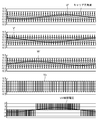
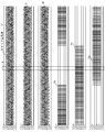
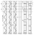
- FIG. 3 is a diagram showing a three-phase modulation voltage command value output by the phase voltage command calculation unit constituting the command value calculation unit of the control unit, a carrier triangle wave, a PWM waveform when performing three-phase modulation control, and a UV line voltage. is there. It is a figure which shows the two-phase modulation voltage command value output by the line modulation calculation unit which constitutes the command value calculation unit of the control unit of FIG. 1, the carrier triangle wave, the PWM waveform output by the PWM signal generation unit, and the UV line voltage. ..
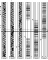
- FIG. 5 is a diagram showing a two-phase modulation voltage command value output by the line modulation calculation unit constituting the command value calculation unit of the control unit, a carrier triangle wave, a corrected PWM waveform output by the duty correction unit, and a line voltage. is there. It is an enlarged view around the frame X of FIG.
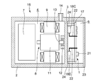
- the electric compressor 16 of the embodiment constitutes a part of a refrigerant circuit of a vehicle air conditioner mounted on a vehicle such as a hybrid vehicle or an electric vehicle, and is a DC power source (battery) mounted on the vehicle. ) 29 is fed and driven.
- FIG. 2 the inside of the metal housing 2 of the electric compressor 16 is divided into a compression mechanism accommodating portion 4 and an inverter accommodating portion 6 by a partition wall 3 intersecting the axial direction of the housing 2. It is partitioned, and for example, a scroll type compression mechanism 7 and a motor 8 for driving the compression mechanism 7 are housed in the compression mechanism accommodating portion 4.
- the motor 8 is an IPMSM (Interior Permanent Magnet Synchronous Motor) including a stator 9 fixed to the housing 2 and a rotor 11 having a built-in permanent magnet that rotates inside the stator 9.
- IPMSM Interior Permanent Magnet Synchronous Motor
- a bearing portion 12 is formed in the central portion of the partition wall 3 on the compression mechanism accommodating portion 4 side, one end of the drive shaft 13 of the rotor 11 is supported by the bearing portion 12, and the other end of the drive shaft 13 is a compression mechanism. It is connected to 7.
- a suction port 14 is formed in the vicinity of the partition wall 3 at a position corresponding to the compression mechanism accommodating portion 4 of the housing 2, and when the rotor 11 (drive shaft 13) of the motor 8 rotates to drive the compression mechanism 7.
- a refrigerant which is a working fluid, flows into the compression mechanism accommodating portion 4 of the housing 2 from the suction port 14, and is sucked into the compression mechanism 7 to be compressed.
- the refrigerant compressed by the compression mechanism 7 to a high temperature and high pressure is discharged to the refrigerant circuit outside the housing 2 from a discharge port (not shown). Further, the low-temperature refrigerant that has flowed in from the suction port 14 passes near the partition wall 3 and passes around the motor 8 and is sucked into the compression mechanism 7, so that the partition wall 3 is also cooled.
- the power conversion device 1 of the present invention that drives and controls the motor 8 is accommodated in the inverter accommodating portion 6 partitioned from the compression mechanism accommodating portion 4 by the partition wall 3.
- the power conversion device 1 is configured to supply power to the motor 8 via a sealed terminal or a lead wire penetrating the partition wall 3.
- the power conversion device 1 includes a substrate 17, six switching elements 18A to 18F wired on one surface side of the substrate 17, and the other surface side of the substrate 17. It is composed of a control unit 21 wired to the above, an HV connector (not shown), an LV connector, and the like.
- the switching elements 18A to 18F are composed of an insulated gate bipolar transistor (IGBT) or the like in which a MOS structure is incorporated in a gate portion.
- IGBT insulated gate bipolar transistor
- the switching element 18B and the switching element 18E on the lower arm side, the switching element 18C on the upper arm side and the switching element 18F on the lower arm side of the W-phase inverter 19W are arranged side by side.
- the switching elements 18A and 18D, the switching elements 18B and 18E, and the switching elements 18C and 18F are arranged radially around the center of the substrate 17.
- the terminal portions 22 of the switching elements 18A to 18F are connected to the substrate 17 in a state of being on the center side of the substrate 17. Then, the power conversion device 1 assembled in this way is housed in the inverter accommodating portion 6 in a state where one side of the switching elements 18A to 18F is on the partition wall 3 side, and is attached to the partition wall 3 to cover the power conversion device 1. It is closed at 23. In this case, the substrate 17 is fixed to the partition wall 3 via the boss portion 24 that stands up from the partition wall 3.
- the switching elements 18A to 18F are brought into close contact with the partition wall 3 directly or via a predetermined insulating heat conductive material, and are in close contact with the partition wall 3 of the housing 2. It becomes a heat exchange relationship. Since the partition wall 3 is cooled by the refrigerant sucked into the compression mechanism accommodating portion 4 as described above, the switching elements 18A to 18F have a heat exchange relationship with the suction refrigerant through the partition wall 3, and the partition wall It is cooled by the refrigerant sucked into the compression mechanism accommodating portion 4 through the thickness of 3, and the switching elements 18A to 18F themselves radiate heat to the refrigerant through the partition wall 3.
- the power conversion device 1 of the embodiment of the present invention includes the above-mentioned three-phase inverter circuit (three-phase inverter circuit) 28 and the control unit 21. I have.
- the inverter circuit 28 is a circuit that converts the DC voltage of the DC power supply (battery) 29 into a three-phase AC voltage and applies it to the armature coil of the stator 9 of the motor 8.
- the inverter circuit 28 has the above-mentioned U-phase inverter 19U, V-phase inverter 19V, and W-phase inverter 19W, and each phase inverter 19U to 19W has the above-mentioned switching elements 18A to 18C on the upper arm side, respectively.
- the switching elements 18D to 18F on the lower arm side are individually provided. Further, flywheel diodes 31 are connected in antiparallel to each of the switching elements 18A to 18F.
- the upper end side of the switching elements 18A to 18C on the upper arm side of the inverter circuit 28 is connected to the positive electrode side of the DC power supply 29 and the smoothing capacitor 32.
- the smoothing capacitor 32 is also provided on the substrate 17 to form the power conversion device 1.
- the lower end side of the switching elements 18D to 18F on the lower arm side of the inverter circuit 28 is connected to the negative electrode side of the DC power supply 29 and the smoothing capacitor 32.
- the switching element 18A on the upper arm side of the U-phase inverter 19U and the switching element 18D on the lower arm side are connected to the U-phase armature coil of the motor 8 to switch the V-phase inverter 19V on the upper arm side.
- the element 18B and the switching element 18E on the lower arm side are connected to the armature coil of the V phase of the motor 8, and the switching element 18C on the upper arm side and the switching element 18F on the lower arm side of the W phase inverter 19W are connected.
- the space is connected to the W-phase armature coil of the motor 8.
- a current detector 30 for detecting the DC current flowing through the inverter circuit 28 is connected to the bus between the DC power supply 29 and the inverter circuit 28.
- the current detector 30 is connected to the bus on the minus side in the embodiment, it may be connected to the bus on the plus side.
- the current detector 30 can be configured by a shunt resistor or a Hall element, but in the embodiment, it is assumed that the current detector 30 is composed of a shunt resistor.
- control unit 21 is composed of a microcomputer having a processor, inputs a rotation speed command value from the vehicle ECU, and receives U-phase current iu and V-phase current iv from the motor 8.
- Each phase current of the W phase current iw is input, and based on these, the ON / OFF states of the switching elements 18A to 18F of the inverter circuit 28 are controlled. Specifically, the gate voltage applied to the gate terminals of the switching elements 18A to 18F is controlled.
- the control unit 21 includes a phase current conversion unit 38, a phase voltage command calculation unit 33, a line modulation calculation unit 34, a PWM signal generation unit 36, a duty correction unit 39, and a gate driver 37. .. Then, the phase voltage command calculation unit 33 and the line modulation calculation unit 34 constitute the command value calculation unit 35 in the present invention.
- phase current conversion unit 38 is based on the direct current detected by the current detector 30 and the switching timing of the switching elements 18A to 18F, and the phase currents of the U-phase current iu, V-phase current iv, and W-phase current iw of the motor 8. Is detected.
- the switching element 18A on the upper arm side of the U-phase inverter 19U is turned on, the switching element 18E on the lower arm side of the V-phase inverter 19V and the switching element 18F on the lower arm side of the W-phase inverter 19W are turned on.
- the U-phase current iu flows from the switching element 18A to the U-phase armature coil of the motor 8
- the V-phase current iv flows from the flywheel diode 31 connected in parallel to the switching element 18E to the V-phase of the motor 8. It flows through the armature coil, and the W-phase current iw flows out from the W-phase armature coil of the motor 8 to the switching element 18F.
- a U-phase current iu flows through the current detector 30 and can be detected.
- the switching element 18A on the upper arm side of the U-phase inverter 19U and the switching element 18B on the upper arm side of the V-phase inverter 19V are turned on, and the switching element 18F on the lower arm side of the W-phase inverter 19W is turned on.
- the U-phase current iu and the V-phase current iv flow from the switching elements 18A and 18B to the U-phase and V-phase armature coils of the motor 8, respectively, and the W-phase current iw is the W-phase inverter of the motor 8. It flows out from the coil to the switching element 18F.
- a W-phase current iw flows through the current detector 30 and can be detected.
- the phase current conversion unit 38 has a minimum time Y required for detecting the phase current by the current detector 30, and the ON period of the switching elements 18A to 18C on the upper arm side within the carrier cycle, or the ON period of the switching elements 18A to 18C on the upper arm side, or If the OFF period is shorter than this minimum time Y, detection is impossible. Then, the phase currents iu, iv, and iwa detected by the phase current conversion unit 38 are input to the phase voltage command calculation unit 33.
- Phase voltage command calculation unit 33 (command value calculation unit 35)
- the phase voltage command calculation unit 33 applies a three-phase modulated voltage command value U'(U) to the armature coil of each phase of the motor 8 based on the electric angle and current command value of the motor 8 and the phase currents iu, iv, and iwa.
- Phase voltage command value V'(V phase voltage command value), W'(W phase voltage command value) are calculated.
- the three-phase modulation voltage command values U', V', and W' are after normalization of the voltage command value with the DC voltage Vdc when performing three-phase modulation control of the motor 8 (corrected to -1 to 1). It is the value of, and is shown in FIG.
- FIG. 3 also shows a carrier triangular wave to be compared by the PWM signal generation unit 36 described later.
- the frequency (carrier frequency) of the carrier triangular wave of the embodiment is set to 20 kHz outside the audible range. This is because when the carrier frequency becomes a frequency in the audible range lower than 20 kHz, the sound generated from the electric compressor 16 is recognized as noise.
- This carrier frequency is also a PWM signal (U phase) described later when Vu shown in FIG. 3 performs three-phase modulation control of the motor 8, and the UV line voltage in FIG. 3 is also three-phase modulation. It is a potential difference between the U phase and the V phase which will be described later when the control is performed.
- Line modulation calculation unit 34 (command value calculation unit 35)
- the line-to-line modulation calculation unit 34 is calculated by the phase voltage command calculation unit 33, and based on the calculated three-phase modulation voltage command values U', V', and W', the two-phase modulation voltage command value U (U-phase voltage command). Value), V (V-phase voltage command value), W (W-phase voltage command value) are calculated. The operation of the line modulation calculation unit 34 will be described in detail later.
- the PWM signal generation unit 36 is calculated by the line modulation calculation unit 34, and based on the calculated two-phase modulation voltage command values U, V, W, the U-phase inverter 19U, the V-phase inverter 19V, and the W phase of the inverter circuit 28
- the PWM signals Vu, Vv, and Vw, which are the drive command signals of the inverter 19W, are generated by comparing the magnitude with the carrier triangular wave.
- Duty correction unit 39 corrects the two-phase modulation voltage command values U, V, and W output from the line modulation calculation unit 34 (command value calculation unit 35), so that the PWM output from the PWM signal generation unit 36 is PWM.
- the signals Vu, Vv, and Vw are corrected and output to the gate driver 37, and the operation of the duty correction unit 39 will be described in detail later.
- Gate driver 37 Based on the PWM signals Vu, Vv, Vw output from the PWM signal generation unit 36, the gate driver 37 has the gate voltages Vu and Vul of the U-phase inverter 19U switching elements 18A and 18D, and the switching element 18B of the V-phase inverter 19V. , 18E gate voltages Vvu and Vvl, and gate voltages Vw and Vwl of the switching elements 18C and 18F of the W-phase inverter 19W are generated.
- These gate voltages Vuu, Vul, Vvu, Vvl, Vwoo, and Vwl can be represented by a duty (ON period of switching elements 18A to 18C on the upper arm side) which is a time ratio of the ON state in a predetermined time.
- each of the switching elements 18A to 18F of the inverter circuit 28 is ON / OFF driven based on the gate voltages Vuu, Vul, Vv, Vvl, Vwoo, and Vwl output from the gate driver 37. That is, when the gate voltage is in the ON state (predetermined voltage value), the transistor is turned on, and when the gate voltage is in the OFF state (zero), the transistor is turned off.
- the gate driver 37 is a circuit for applying a gate voltage to the IGBT based on the PWM signal, and is composed of a photocoupler, a logic IC, a transistor, and the like.
- the two-phase modulation voltage command values U, V, and W calculated by the line-to-line modulation calculation unit 34 are after normalization of the voltage command value for performing two-phase modulation control of the motor 8 with the DC voltage Vdc (-1 to 1 to). It is a value after correction to 1), and an example is shown in FIG. Note that FIG. 4 also shows a carrier triangular wave compared by the PWM signal generation unit 36 at the same time. Further, Vu shown in FIG. 4 is a PWM signal (U phase) for performing two-phase modulation control of the motor 8, and the UV line voltage in FIG. 4 is between U phase and V phase in two-phase modulation control. Is the potential difference of.
- the line-to-line modulation calculation unit 34 has a U-phase voltage command value U', a V-phase voltage command value V', and a W-phase voltage command, which are three-phase modulation voltage command values of each phase calculated by the phase voltage command calculation unit 33.
- the U-phase voltage command value U which is a two-phase modulation voltage command value for fixing the ON / OFF state of the switching elements 18A to 18F of the phase having the maximum absolute value to the ON / OFF state by comparing the values W', and V
- By calculating and outputting the phase voltage command value V and the W phase voltage command value W two-phase modulation control that reduces the number of switchings of the switching elements 18A to 18F compared to the case of performing three-phase modulation control is performed. Execute.
- the line modulation calculation unit 34 of the embodiment compares each value as shown in the following equations (i) to (iii). Set the values U'comp, V'comp, W'comp.
- U'comp U' ⁇ ⁇ ⁇ (i)
- V'comp V' ⁇ ⁇ ⁇ (ii)
- W'comp W' ⁇ ⁇ ⁇ (iii)
- the U-phase voltage command value U, the V-phase voltage command value V, and the W-phase voltage command value which are the two-phase modulation voltage command values, are used using the following equations (vi) to (viii).
- U U'-K + sign (K) ...
- V V'-K + sign (K) ...
- W W'-K + sign (K) ... (viii)
- sign (K) is defined as "1" when K is a positive value and "-1" when K is a negative value.
- V-phase voltage command value V' is K and the comparison value V'comp is the maximum value K1
- the V-phase voltage command value V becomes "1"
- the comparison value V'comp is the minimum value K2.
- the V-phase voltage command value V becomes “-1”.
- the ON / OFF states of the switching elements 18B and 18E of the V-phase inverter 19V are fixed during the period when the V-phase voltage command value V'is K, and the number of switchings is reduced accordingly.
- the W-phase voltage command value W'is K and the comparison value W'comp is the maximum value K1
- the W-phase voltage command value W becomes "1"
- the comparison value W'comp is the minimum value K2.
- the W-phase voltage command value W becomes “-1”.
- the ON / OFF states of the switching elements 18C and 18F of the W-phase inverter 19W are fixed during the period when the W-phase voltage command value W'is K, and the number of switchings is reduced accordingly.
- FIG. 4 shows a U-phase voltage command value U, a V-phase voltage command value V, and a W-phase voltage command value W output from the line modulation calculation unit 34, and a U-phase PWM signal Vu output from the PWM signal generation unit 36. And the UV line voltage.
- FIG. 5 shows the two-phase modulation voltage command values U, V, W output by the line modulation calculation unit 34, the carrier triangle wave, and the PWM signals Vu, Vv, Vw output by the PWM signal generation unit 36
- FIG. 6 shows FIG. An enlarged view of the vicinity of the frame X inside is shown.
- FIGS. 5 to 8 is a two-phase modulation control in which the switching element on the upper arm side of any one phase is fixed in the OFF state and the switching element on the lower arm side is fixed in the ON state.
- the PWM signal Vu is a drive command signal for the U-phase inverter 19U of the inverter circuit 28, and the pulse width of “1” shown in FIGS. 5 and 6 is the duty within one carrier cycle. It is the ON period of the switching element 18A on the arm side. That is, during this duty (width of the pulse of "1"), the switching element 18A on the upper arm side is turned on, and the switching element 18D on the lower arm side is turned off.
- the PWM signal Vv is a drive command signal of the V-phase inverter 19V
- the width of the pulse of "1" shown in FIGS. 5 and 6 is the duty within one carrier cycle, and is on the upper arm side.
- the ON period of the switching element 18B is reached. That is, during this duty (width of the pulse of "1"), the switching element 18B on the upper arm side is turned on, and the switching element 18E on the lower arm side is turned off.
- the PWM signal Vw is a drive command signal of the W-phase inverter 19W
- the width of the pulse of “1” shown in FIGS. 5 and 6 is the duty within one carrier cycle, and is on the upper arm side.
- the ON period of the switching element 18C is reached. That is, during this duty (width of the pulse of "1"), the switching element 18C on the upper arm side is turned on, and the switching element 18F on the lower arm side is turned off.
- the switching element 18A on the upper arm side of the U phase is fixed in the OFF state. Then, when the phase current is detected during the ON period of the switching elements 18B and 18C on the upper arm side of the V phase and the W phase, as shown in FIG. 6, the switching elements 18B and 18C on the upper arm side within one carrier cycle. When the ON period of is shorter than this minimum time Y, it becomes impossible to detect the phase currents of the V phase and the W phase.
- the U-phase current iu can be detected, the V-phase current iv and the W-phase current iwa cannot be detected, so that the three-phase phase currents iu, iv, and iwa cannot be detected.
- the duty correction unit 39 of the control unit 21 receives a line modulation calculation unit 34 (command) as shown in FIGS. 7 and 8 when the voltage utilization rate kH of the motor 8 drops to a predetermined voltage utilization rate kH1 or less.
- the two-phase modulation voltage command values U, V, and W output from the value calculation unit 35) are corrected, and the PWM signals Vu, Vv, and Vw output from the PWM signal generation unit 36 are corrected.
- the ON period (indicated by P1 in FIG. 8) of the switching element 18B having a specific carrier period Z1 of the V phase is corrected to be equal to or longer than the above-mentioned minimum time Y.
- the ON period (indicated by P2 in FIG. 8) of the switching element 18B having the carrier period Z2 of the V phase is set to the minimum value that can be output.
- the duty correction unit 39 sets the sum of the duties of the switching elements 18B in the corrected two carrier cycles (Z1 to Z2) shown in FIG. 8 into the two carrier cycles (Z1 to Z2) before the correction in FIG. Matches the sum of the duties of the switching element 18B in. Further, the duty correction unit 39 provides the ON period of the switching element 18B in the first half of the specific carrier period Z1 of the V phase, and provides the ON period of the switching element 18B in the latter half of the other carrier period Z2 of the V phase.
- the duty correction unit 39 also performs another carrier cycle of the W phase (next carrier cycle of Z2) during the ON period of the switching element 18C on the upper arm side of the W phase of the specific carrier cycle Z2 of the W phase. ), By moving and adding a part of the ON period of the switching element 18C, the ON period of the switching element 18C of the specific carrier period Z2 of the W phase (indicated by P3 in FIG. 8) is set to the above-mentioned minimum time. Make corrections that are Y or greater. On the other hand, the ON period of the switching element 18C having another carrier cycle of the W phase is set to the minimum value that can be output in the same manner.
- the duty correction unit 39 sets the sum of the duties of the switching element 18C in the corrected two carrier cycles (Z2 and the next cycle) shown in FIG. 8 as the two carrier cycles before the correction in FIG. It is matched with the sum of the duties of the switching element 18C at (Z2 and the next cycle). Further, the duty correction unit 39 provides the ON period of the switching element 18C in the first half of the specific carrier period Z2 of the W phase, and ONs the switching element 18C in the latter half of the other carrier period of the W phase (the cycle next to Z2). Set a period.
- the above correction is similarly executed for other timings (a set of a specific carrier cycle and another carrier cycle).
- the other carrier cycle is not limited to one, and a part of each of those ON periods is moved from two or more (plural) carrier cycles following the specific carrier cycle to the ON period of the specific carrier cycle. It may be.
- the phase current converter 38 can detect the V-phase current iv in the carrier cycle Z1 and the W-phase current iv in the carrier cycle Z2 by the current detector 30, and finally three-phase. It is possible to detect the minute phase currents iu, iv, and iwa. In this case, for example, since the ON period of the switching element 18B and the ON period of the switching element 18C in the carrier cycle Z2 do not overlap, the V-phase current iv and the W-phase current iwa can be detected without any trouble.
- the duty correction unit 39 of the control unit 21 performs another carrier during the ON period of the switching element (18B in the V phase) of the inverter circuit 28 in a specific carrier cycle (Z1 in the V phase).
- the switching element (Z1 in V phase) in a specific carrier period (Z1 in V phase) is added.
- the ON period of 18B is corrected to be equal to or longer than the minimum time Y required for detecting the current by the current detector 30, for example, in the power conversion device 1 of the two-phase modulation method as in the embodiment, As in the embodiment, the voltage utilization rate kH of the motor 8 becomes low, the OFF state of the switching element 18A on the upper arm side of the U phase of the inverter circuit 28 is fixed, and the OFF state of the upper arm side of the other two phases is fixed. Even when the ON period of the switching elements 18B and 18C is shorter than the minimum time Y within one carrier cycle, the minimum time Y or more for current detection by the current detector 30 in a specific carrier cycle (Z1 in the V phase). The ON period is secured, and the phase current (iv in the carrier cycle Z1 of the V phase) can be detected.
- the duty correction unit 39 sets a part of the ON period of the switching element (18B in the V phase) in another carrier period (Z2 in the V phase) to the switching element (Z1 in the V phase) having a specific carrier period (Z1 in the V phase). Since it is added to the ON period of 18B), it is possible to prevent the generation of noise due to the decrease in the carrier frequency.
- the duty correction unit 39 makes the sum of the duties in the specific carrier cycle (Z1 in the V phase) and the duty in the other carrier cycle (Z2 in the V phase) match before and after the correction. Therefore, it is possible to realize high-quality motor control without causing deterioration of the controllability of the motor 8.
- the duty correction unit 39 corrects the corrected ON period of the switching element (18B in the V phase) in another carrier cycle (Z2 in the V phase) to be the minimum value that can be output. Therefore, even if the motor 8 rotates at a low speed, it is possible to secure an ON period of Y or more, which is the minimum time for current detection by the current detector 30, in a specific carrier cycle (Z1 in the V phase) without any problem. Will be.
- the duty correction unit 39 provides a corrected ON period of the switching element (18B in the V phase) in the first half of the specific carrier cycle (Z1 in the V phase), and provides another carrier cycle (Z1 in the V phase). Since the corrected ON period of the switching element (18B in the V phase) is provided in the latter half of Z2), the phase of the ON period does not overlap with other phases, and a specific carrier period (Z1 in the V phase) is provided. , In the W phase, the phase currents iv and iwa can be easily detected in Z2)).
- a part of the ON period of the switching element in another carrier cycle is moved and added to the ON period of the switching element of the inverter circuit 28 in a specific carrier cycle.
- the phase switching element is fixed in the ON state and the other two-phase switching element is switched, the OFF period of the switching element in a specific carrier cycle and the OFF period of the switching element in the other carrier cycle
- the OFF period of the switching element in a specific carrier cycle may be corrected to be equal to or longer than the minimum time Y required for detecting the current by the current detector 30. ..
- the present invention has been described with the two-phase modulation type power conversion device 1 in which the one-phase switching element is fixed in the OFF state and the other two-phase switching elements are switched, but the present invention is not limited to this.
- the present invention is also effective in a method of fixing the switching element of the above to the ON state and the OFF state.
- the duty correction unit corrects the three-phase modulation voltage command values U', V', and W'output by the phase voltage command calculation unit 33 in the same manner as described above.
- the present invention is applied to the power converter 1 that drives and controls the motor 8 of the electric compressor 16, but the present invention is not limited to this, and the present invention is effective for the drive control of the motors of various devices.
- Power converter 8 Motor 16 Electric compressor 18A-18F Switching element 19U U-phase inverter 19V V-phase inverter 19W W-phase inverter 21 Control unit 28 Three-phase inverter circuit 30 Current detector 33 Phase voltage command calculation unit 34 Line modulation calculation Part 35 Command value calculation part 36 PWM signal generation part 37 Gate driver 38 Phase current conversion part 39 Duty correction part
Landscapes
- Engineering & Computer Science (AREA)
- Power Engineering (AREA)
- Inverter Devices (AREA)
Abstract
Le problème décrit par la présente invention consiste à fournir un dispositif de conversion de puissance qui peut détecter un courant de phase sans générer de bruit et sans entrave même dans des situations dans lesquelles la vitesse du moteur est faible et le courant continu dans un circuit onduleur est difficile à détecter. Pendant la période de marche des éléments de commutation (18B, 18C) d'un circuit onduleur (28) dans un cycle de porteuse spécifique, une unité de correction de rapport cyclique (39) destinée à corriger le rapport cyclique d'un signal PWM corrige la période de marche des éléments de commutation dans le cycle de porteuse spécifique pour avoir au moins le temps minimal Y nécessaire pour que le détecteur de courant (30) détecte le courant en déplaçant et en ajoutant une partie des périodes de marche desdits éléments de commutation (18B, 18C) dans un autre cycle de porteuse.
Priority Applications (2)
| Application Number | Priority Date | Filing Date | Title |
|---|---|---|---|
| CN202080049102.6A CN114128131B (zh) | 2019-06-04 | 2020-05-28 | 功率转换装置 |
| EP20818334.3A EP3979485A4 (fr) | 2019-06-04 | 2020-05-28 | Dispositif de conversion de puissance |
Applications Claiming Priority (2)
| Application Number | Priority Date | Filing Date | Title |
|---|---|---|---|
| JP2019104361A JP7221802B2 (ja) | 2019-06-04 | 2019-06-04 | 電力変換装置 |
| JP2019-104361 | 2019-06-04 |
Publications (1)
| Publication Number | Publication Date |
|---|---|
| WO2020246355A1 true WO2020246355A1 (fr) | 2020-12-10 |
Family
ID=73649464
Family Applications (1)
| Application Number | Title | Priority Date | Filing Date |
|---|---|---|---|
| PCT/JP2020/021041 Ceased WO2020246355A1 (fr) | 2019-06-04 | 2020-05-28 | Dispositif de conversion de puissance |
Country Status (4)
| Country | Link |
|---|---|
| EP (1) | EP3979485A4 (fr) |
| JP (1) | JP7221802B2 (fr) |
| CN (1) | CN114128131B (fr) |
| WO (1) | WO2020246355A1 (fr) |
Cited By (1)
| Publication number | Priority date | Publication date | Assignee | Title |
|---|---|---|---|---|
| WO2023100868A1 (fr) * | 2021-12-01 | 2023-06-08 | サンデン株式会社 | Dispositif de conversion de puissance |
Families Citing this family (1)
| Publication number | Priority date | Publication date | Assignee | Title |
|---|---|---|---|---|
| CN114825892B (zh) | 2022-05-27 | 2023-08-11 | 杭州晶丰明源半导体有限公司 | 最小导通时间电路、控制器、电路系统和电流检测方法 |
Citations (5)
| Publication number | Priority date | Publication date | Assignee | Title |
|---|---|---|---|---|
| JPH08340691A (ja) | 1995-06-08 | 1996-12-24 | Nippondenso Co Ltd | インバータ制御装置 |
| JP2008113494A (ja) * | 2006-10-30 | 2008-05-15 | Mitsubishi Electric Corp | 3相pwm信号発生装置および3相電圧型インバータ装置 |
| JP2010213407A (ja) * | 2009-03-09 | 2010-09-24 | Hitachi Industrial Equipment Systems Co Ltd | 電力変換装置及びその制御方法 |
| JP4788416B2 (ja) | 2006-03-15 | 2011-10-05 | パナソニック株式会社 | モータ駆動用インバータ制御装置及び冷凍装置 |
| JP2012125022A (ja) * | 2010-12-07 | 2012-06-28 | Denso Corp | 電力変換装置 |
Family Cites Families (8)
| Publication number | Priority date | Publication date | Assignee | Title |
|---|---|---|---|---|
| JP4866216B2 (ja) * | 2006-11-22 | 2012-02-01 | 株式会社日立製作所 | 電力変換装置 |
| US20130147408A1 (en) * | 2010-09-15 | 2013-06-13 | Panasonic Corporation | Motor current phase detecting device and motor drive device having same |
| JP5790390B2 (ja) * | 2011-10-07 | 2015-10-07 | アイシン精機株式会社 | 交流モータの制御装置および制御方法 |
| JP6170455B2 (ja) * | 2014-03-20 | 2017-07-26 | 日立オートモティブシステムズ株式会社 | ブラシレスモータの制御装置及び制御方法 |
| JP6156282B2 (ja) * | 2014-08-07 | 2017-07-05 | 株式会社デンソー | 回転機の制御装置 |
| KR101986035B1 (ko) * | 2015-04-20 | 2019-06-04 | 닛산 지도우샤 가부시키가이샤 | 전동 수단 제어 장치 및 제어 방법 |
| JP6369423B2 (ja) * | 2015-09-01 | 2018-08-08 | 株式会社安川電機 | 電力変換装置、制御装置および制御方法 |
| CN107317502B (zh) * | 2016-04-18 | 2023-07-18 | 珠海格力电器股份有限公司 | 逆变器死区补偿方法、装置和逆变器 |
-
2019
- 2019-06-04 JP JP2019104361A patent/JP7221802B2/ja active Active
-
2020
- 2020-05-28 EP EP20818334.3A patent/EP3979485A4/fr active Pending
- 2020-05-28 WO PCT/JP2020/021041 patent/WO2020246355A1/fr not_active Ceased
- 2020-05-28 CN CN202080049102.6A patent/CN114128131B/zh active Active
Patent Citations (5)
| Publication number | Priority date | Publication date | Assignee | Title |
|---|---|---|---|---|
| JPH08340691A (ja) | 1995-06-08 | 1996-12-24 | Nippondenso Co Ltd | インバータ制御装置 |
| JP4788416B2 (ja) | 2006-03-15 | 2011-10-05 | パナソニック株式会社 | モータ駆動用インバータ制御装置及び冷凍装置 |
| JP2008113494A (ja) * | 2006-10-30 | 2008-05-15 | Mitsubishi Electric Corp | 3相pwm信号発生装置および3相電圧型インバータ装置 |
| JP2010213407A (ja) * | 2009-03-09 | 2010-09-24 | Hitachi Industrial Equipment Systems Co Ltd | 電力変換装置及びその制御方法 |
| JP2012125022A (ja) * | 2010-12-07 | 2012-06-28 | Denso Corp | 電力変換装置 |
Non-Patent Citations (1)
| Title |
|---|
| See also references of EP3979485A4 |
Cited By (3)
| Publication number | Priority date | Publication date | Assignee | Title |
|---|---|---|---|---|
| WO2023100868A1 (fr) * | 2021-12-01 | 2023-06-08 | サンデン株式会社 | Dispositif de conversion de puissance |
| JP2023081503A (ja) * | 2021-12-01 | 2023-06-13 | サンデン株式会社 | 電力変換装置 |
| JP7822760B2 (ja) | 2021-12-01 | 2026-03-03 | サンデン株式会社 | 電力変換装置 |
Also Published As
| Publication number | Publication date |
|---|---|
| CN114128131B (zh) | 2024-09-17 |
| JP2020198724A (ja) | 2020-12-10 |
| EP3979485A4 (fr) | 2023-02-15 |
| JP7221802B2 (ja) | 2023-02-14 |
| EP3979485A1 (fr) | 2022-04-06 |
| CN114128131A (zh) | 2022-03-01 |
Similar Documents
| Publication | Publication Date | Title |
|---|---|---|
| US9203330B2 (en) | Motor control device and air conditioner | |
| US9287820B2 (en) | Motor control device and air conditioner | |
| JP6963495B2 (ja) | 電力変換装置 | |
| JP5521914B2 (ja) | 電力変換装置、及び、これを用いた電動パワーステアリング装置 | |
| KR20180040085A (ko) | 차량용 인버터 구동 장치 및 차량용 유체 기계 | |
| CN106026724A (zh) | 用于电力逆变器的控制装置 | |
| CN116114162B (zh) | 逆变器装置 | |
| US11677309B2 (en) | Inverter device | |
| JP7221802B2 (ja) | 電力変換装置 | |
| JP6982519B2 (ja) | 電力変換装置 | |
| CN112567620B (zh) | 逆变装置 | |
| JP7221726B2 (ja) | インバータ装置 | |
| JP2009273302A (ja) | 電動モータの制御装置 | |
| CN108352801A (zh) | 电动机的控制装置及使用其的电动汽车 | |
| JP5441862B2 (ja) | インバータ制御装置、圧縮機駆動装置、空気調和機 | |
| JP7727833B2 (ja) | モータ制御装置、モータ制御方法 | |
| JP2025022607A (ja) | インバータ装置及びそれを備えた電動圧縮機 | |
| JP2018183004A (ja) | インバータ制御装置 | |
| JP2025122731A (ja) | 電力変換装置 |
Legal Events
| Date | Code | Title | Description |
|---|---|---|---|
| 121 | Ep: the epo has been informed by wipo that ep was designated in this application |
Ref document number: 20818334 Country of ref document: EP Kind code of ref document: A1 |
|
| NENP | Non-entry into the national phase |
Ref country code: DE |
|
| ENP | Entry into the national phase |
Ref document number: 2020818334 Country of ref document: EP Effective date: 20220103 |