WO2020255338A1 - 電力変換装置 - Google Patents
電力変換装置 Download PDFInfo
- Publication number
- WO2020255338A1 WO2020255338A1 PCT/JP2019/024526 JP2019024526W WO2020255338A1 WO 2020255338 A1 WO2020255338 A1 WO 2020255338A1 JP 2019024526 W JP2019024526 W JP 2019024526W WO 2020255338 A1 WO2020255338 A1 WO 2020255338A1
- Authority
- WO
- WIPO (PCT)
- Prior art keywords
- command value
- voltage command
- dead zone
- value
- correction
- Prior art date
- Legal status (The legal status is an assumption and is not a legal conclusion. Google has not performed a legal analysis and makes no representation as to the accuracy of the status listed.)
- Ceased
Links
Images




Classifications
-
- H—ELECTRICITY
- H02—GENERATION; CONVERSION OR DISTRIBUTION OF ELECTRIC POWER
- H02M—APPARATUS FOR CONVERSION BETWEEN AC AND AC, BETWEEN AC AND DC, OR BETWEEN DC AND DC, AND FOR USE WITH MAINS OR SIMILAR POWER SUPPLY SYSTEMS; CONVERSION OF DC OR AC INPUT POWER INTO SURGE OUTPUT POWER; CONTROL OR REGULATION THEREOF
- H02M1/00—Details of apparatus for conversion
- H02M1/38—Means for preventing simultaneous conduction of switches
- H02M1/385—Means for preventing simultaneous conduction of switches with means for correcting output voltage deviations introduced by the dead time
-
- H—ELECTRICITY
- H02—GENERATION; CONVERSION OR DISTRIBUTION OF ELECTRIC POWER
- H02M—APPARATUS FOR CONVERSION BETWEEN AC AND AC, BETWEEN AC AND DC, OR BETWEEN DC AND DC, AND FOR USE WITH MAINS OR SIMILAR POWER SUPPLY SYSTEMS; CONVERSION OF DC OR AC INPUT POWER INTO SURGE OUTPUT POWER; CONTROL OR REGULATION THEREOF
- H02M1/00—Details of apparatus for conversion
- H02M1/38—Means for preventing simultaneous conduction of switches
-
- H—ELECTRICITY
- H02—GENERATION; CONVERSION OR DISTRIBUTION OF ELECTRIC POWER
- H02M—APPARATUS FOR CONVERSION BETWEEN AC AND AC, BETWEEN AC AND DC, OR BETWEEN DC AND DC, AND FOR USE WITH MAINS OR SIMILAR POWER SUPPLY SYSTEMS; CONVERSION OF DC OR AC INPUT POWER INTO SURGE OUTPUT POWER; CONTROL OR REGULATION THEREOF
- H02M7/00—Conversion of AC power input into DC power output; Conversion of DC power input into AC power output
- H02M7/42—Conversion of DC power input into AC power output without possibility of reversal
- H02M7/44—Conversion of DC power input into AC power output without possibility of reversal by static converters
- H02M7/48—Conversion of DC power input into AC power output without possibility of reversal by static converters using discharge tubes with control electrode or semiconductor devices with control electrode
- H02M7/483—Converters with outputs that each can have more than two voltages levels
- H02M7/487—Neutral point clamped inverters
-
- H—ELECTRICITY
- H02—GENERATION; CONVERSION OR DISTRIBUTION OF ELECTRIC POWER
- H02M—APPARATUS FOR CONVERSION BETWEEN AC AND AC, BETWEEN AC AND DC, OR BETWEEN DC AND DC, AND FOR USE WITH MAINS OR SIMILAR POWER SUPPLY SYSTEMS; CONVERSION OF DC OR AC INPUT POWER INTO SURGE OUTPUT POWER; CONTROL OR REGULATION THEREOF
- H02M7/00—Conversion of AC power input into DC power output; Conversion of DC power input into AC power output
- H02M7/42—Conversion of DC power input into AC power output without possibility of reversal
- H02M7/44—Conversion of DC power input into AC power output without possibility of reversal by static converters
- H02M7/48—Conversion of DC power input into AC power output without possibility of reversal by static converters using discharge tubes with control electrode or semiconductor devices with control electrode
- H02M7/53—Conversion of DC power input into AC power output without possibility of reversal by static converters using discharge tubes with control electrode or semiconductor devices with control electrode using devices of a triode or transistor type requiring continuous application of a control signal
- H02M7/537—Conversion of DC power input into AC power output without possibility of reversal by static converters using discharge tubes with control electrode or semiconductor devices with control electrode using devices of a triode or transistor type requiring continuous application of a control signal using semiconductor devices only, e.g. single switched pulse inverters
- H02M7/5387—Conversion of DC power input into AC power output without possibility of reversal by static converters using discharge tubes with control electrode or semiconductor devices with control electrode using devices of a triode or transistor type requiring continuous application of a control signal using semiconductor devices only, e.g. single switched pulse inverters in a bridge configuration
- H02M7/53871—Conversion of DC power input into AC power output without possibility of reversal by static converters using discharge tubes with control electrode or semiconductor devices with control electrode using devices of a triode or transistor type requiring continuous application of a control signal using semiconductor devices only, e.g. single switched pulse inverters in a bridge configuration with automatic control of output voltage or current
Definitions
- This application relates to a power converter.
- the PWM pulse applied to the three-level inverter is generally created by comparing the command voltage with the triangular wave carrier.
- the PWM pulse generation method an example of double carrier unipolar modulation is described in paragraph 0002 and FIG. According to FIG. 8, one command voltage and two triangular wave carriers having different levels are compared. The switching element is conducted while the command voltage exceeds the triangular wave carrier.
- a dead time is provided in order to prevent an arm short circuit from occurring in the arm circuit of the inverter circuit.
- the dead time is a delay time for shifting the on / off timing of a plurality of semiconductor switching elements.
- the length of the dead time determines how much the turn-on edge of the PWM pulse is delayed.
- FIG. 9 is a diagram for explaining the double carrier modulation method.
- the intersection of the AC voltage command values V * u , V * v , V * w and the zero value of the voltage command value is also called "zero cross”.
- a broken line frame representing “region near zero cross X0” is shown.
- the region near zero cross X0 is a region near zero cross of the AC voltage command value.
- the waveform tips of the two triangular wave carrier signals CW1 and CW2 are arranged. Since the tip widths of the triangular wave carrier signals CW1 and CW2 are narrow, the PWM pulse width tends to be narrowly generated in the vicinity of the zero cross of the AC voltage command values V * u , V * v , and V * w .
- This application was made to solve the above-mentioned problems, and an object of the present application is to provide an improved power conversion device so that the controllability does not deteriorate near the zero cross of the voltage command value.
- the power converter for this application is A three-level inverter circuit that includes multiple semiconductor switching elements, An inverter control circuit that outputs a gate signal for driving the three-level inverter circuit in a double carrier modulation method, With The inverter control circuit A command value calculation unit that generates a three-phase output voltage command value including one AC voltage command value and two other AC voltage command values based on the output current and output voltage of the three-level inverter circuit.
- a command value correction unit that outputs a corrected command value after correcting the three-phase output voltage command value, and A gate signal generator that generates the gate signal based on the corrected command value, With The command value correction unit replaces the one AC voltage command value during the dead band passage period, which is the period during which the one AC voltage command value passes through a predetermined dead band around the zero value of the voltage command value.
- the predetermined voltage command value corresponding to the end of the dead zone is output to, and the difference between the one AC voltage command value and the predetermined voltage command value in the dead zone passing period is distributed to the other two AC voltage command values. It was built to do.
- a dead zone is set near the zero cross.
- a certain limit can be given to the AC voltage command value so that the small value closest to the zero cross is not set as the AC voltage command value.
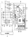
- FIG. 1 is a diagram showing a configuration of a power conversion device 1 according to an embodiment.
- the power conversion device 1 converts the DC power from the DC power supply 2 into three-phase AC power.
- the power conversion device 1 includes input capacitors C1 and C2, a three-level inverter circuit 10, an inverter control circuit 20, a current transformer (CT) 11, and an instrument transformer (VT) 12.
- CT current transformer
- VT instrument transformer
- the three-level inverter circuit 10 includes a plurality of semiconductor switching elements 3.
- the three-level inverter circuit 10 is a neutral point switch type inverter circuit.
- the semiconductor switching element 3 is a power semiconductor element such as an insulated gate bipolar transistor (IGBT).
- the three-level inverter circuit 10 includes an arm circuit.
- the arm circuit is a circuit in which a plurality of semiconductor switching elements 3 are connected in series.
- the positive electrode output of the DC power supply 2 and the high-side bus of the three-level inverter circuit 10 are connected, and a high-side potential V + is applied to this high-side bus.
- the negative electrode output of the DC power supply 2 and the low-side bus of the three-level inverter circuit 10 are connected, and the low-side potential V ⁇ is applied to this low-side bus.
- One end of the series circuit consisting of the input capacitors C1 and C2 is connected to the above high side bus.
- the other end of the series circuit including the input capacitors C1 and C2 is connected to the low-side bus.
- the neutral point potential V0 is given from the connection point between the input capacitor C1 and the input capacitor C2.
- a gate pulse which is a gate signal, is applied to the control electrode of the semiconductor switching element 3.
- the gate pulse is generated by the inverter control circuit 20.
- the gate pulse is a pulse width modulation (PWM) pulse.
- PWM pulse width modulation
- the current transformer 11 and the instrument transformer 12 convert the three-phase output currents Iu, Iv, Iw of the three-level inverter circuit 10 and the three-phase output voltages Vu, Vv, Vw and transmit them to the inverter control circuit 20.
- the inverter control circuit 20 includes a power calculation unit 21, feedback control units 22a and 22b, an inverter voltage command calculation unit 23 that generates a voltage command value V * , a command value correction unit 24, and a gate signal generation unit 25.
- the three-phase output voltage command value is calculated according to the following calculation logic.
- the power calculation unit 21 calculates the active power measurement value and the reactive power measurement value based on the measurement values of the plurality of instrument transformers 12 and the measurement values of the plurality of current transformers 11.
- the inverter control circuit 20 receives a command value from an inverter voltage command calculation unit (not shown) provided outside the inverter control circuit 20.
- the command value includes an active power command value P * and a reactive power command value Q * .
- the active power difference ⁇ P is calculated in the first subtraction block.
- the active power difference ⁇ P is the difference between the active power measurement value P from the power calculation unit 21 and the active power command value P * .
- the reactive power difference ⁇ Q is calculated in the second subtraction block.
- the reactive power difference ⁇ Q is the difference between the reactive power measurement value Q from the power calculation unit 21 and the reactive power command value Q * .
- the feedback control unit 22a implements known feedback control with respect to the active power difference ⁇ P.
- the feedback control unit 22b performs known feedback control with respect to the reactive power difference ⁇ Q.
- any one of PI control, P control and PID control can be used.
- the inverter voltage command calculation unit 23 generates a three-phase voltage command value based on the active power command value from the feedback control unit 22a and the reactive power command value from the feedback control unit 22b. That is, the inverter voltage command calculation unit 23 is a power calculation unit 21, a subtraction block, and a feedback control unit 22a based on the three-phase output currents Iu, Iv, Iw and the three-phase output voltages Vu, Vv, Vw of the three-level inverter circuit 10. , 22b receives a series of control processing results.
- the inverter voltage command calculation unit 23 Based on this series of control processing results, the inverter voltage command calculation unit 23 generates three-phase output voltage command values V * u1 , V * v1 , and V * w1 .
- Inverter control so that the three-phase output voltage command value is set according to MPPT ((Maximum Power Point Tracking) control) as a modification of the embodiment instead of the calculation logic based on the active power and reactive power as described above.
- the circuit 20 may be constructed.
- the setting of the three-phase output voltage command value by MPPT control according to such a modification can be used, for example, when the DC power supply 2 is a solar cell array.
- Three-phase output voltage command values V * u1 , V * v1 , V * w1 are first-phase AC voltage command values V * u1 and second-phase AC voltage command values V * v1 and third-phase AC voltage command values V *. Includes w1 .
- the command value correction unit 24 outputs the corrected command values V * u2 , V * v2 , and V * w2 after correcting the three-phase output voltage command values V * u1 , V * v1 , and V * w1 .
- the command value correction unit 24 gives a predetermined voltage command corresponding to the end of the dead band DB instead of "one AC voltage command value passing through the dead band DB" in the dead band passing period T DB.
- the value V DB is output.
- the dead zone passing period T DB is a period during which one of the three-phase output voltage command values V * u1 , V * v1 , and V * w1 passes through the dead band DB.
- the width of the dead zone DB is determined by the dead zone upper limit value V DBH and the dead zone lower limit value V DBL .
- the dead band upper limit value V DBH and the dead band lower limit value V DBL are values that determine the positive end and the negative end of the dead band DB, and these are also referred to as predetermined voltage command values V DB .
- the command value correction unit 24 outputs a predetermined voltage command value V DB to the dead zone passage period T DB , and distributes the difference ⁇ V * to “the other two AC voltage command values”.
- the "other two AC voltage command values” are the two AC voltage command values existing outside the dead zone DB among the three-phase output voltage command values V * u1 , V * v1 , and V * w1. ..
- the difference ⁇ V * is the difference between one AC voltage command value passing through the dead zone DB and a predetermined voltage command value V DB in the dead zone passing period T DB .
- the corrected command values V * u2 , V * v2 , and V * w2 are output.
- the corrected command values V * u2 , V * v2 , and V * w2 are the corrected first-phase AC voltage command value V * u2 and the corrected second-phase AC voltage command value V * v2 and the corrected third-phase AC voltage.
- the command value V * w2 is included.
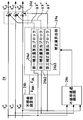
- FIG. 2 is a diagram showing a configuration of a command value correction unit 24 included in the power conversion device 1 according to the embodiment.
- 3 to 6 are time charts for explaining the operation of the command value correction unit 24 according to the embodiment.
- the three-phase output voltage command values V * u1 , V * v1 , and V * w1 are shown in the upper part of FIG.
- the corrected command values V * u2 , V * v2 , and V * w2 are shown in the lower part of FIG.
- the correction amount ⁇ V * used for the correction is shown in the middle part of FIG.
- the first zero cross zx1, the second zero cross zx2, the third zero cross zx3, the fourth zero cross zx4, the fifth zero cross zx5, and the sixth zero cross zx6 arrive repeatedly in this order.
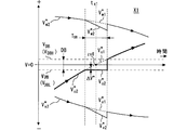
- FIG. 4 is an enlarged view of the broken line portion X1 indicating the vicinity of the time tx1 in FIG.
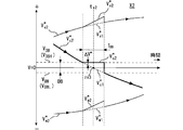
- FIG. 5 is an enlarged view of the broken line portion X2 indicating the vicinity of the time tx2 in FIG.
- One AC voltage command value refers to any one of the three-phase output voltage command values V * u1 , V * v1 , and V * w1 .
- one AC voltage command value is mainly used to distinguish the AC voltage command value passing through the dead zone DB from other AC voltage command values.
- “one AC voltage command value” may be associated with the AC voltage command value of a specific phase, but “one AC voltage command value” is the three-phase output voltage command value V *. Any of u1 , V * v1 , and V * w1 may be substituted.
- the “other two AC voltage command values” are the remaining two ACs of the three-phase output voltage command values V * u1 , V * v1 , and V * w1 excluding the above one AC voltage command value. Refers to the voltage command value.
- the term "the other two AC voltage command values” is mainly used to refer to the AC voltage command value outside the dead zone DB.
- the command value correction unit 24 includes a correction amount calculation unit 24a, a dead zone setting unit 24b, a dead zone passage detection unit 24c, and a correction calculation unit 24d.
- the dead zone setting unit 24b is a block for setting the width of the dead zone DB.
- the dead zone setting unit 24b is constructed so that the dead zone upper limit value V DBH and the dead zone lower limit value V DBL can be set and changed respectively.
- the dead zone upper limit value V DBH and the dead band lower limit value V DBL are set so that the positive and negative signs are opposite and have the same magnitude.
- the dead zone passage detection unit 24c detects the dead zone passage period T DB .
- the dead zone passing period T DB is a period during which one AC voltage command value passes through the dead band DB.
- the dead zone passage detection unit 24c detects the period between the time when one AC voltage command value enters the dead zone DB and the time when this one AC voltage command value leaves the dead zone DB as the dead zone passage period T DB .
- FIG. 4 shows, as an example of the correction operation, the correction operation performed during the period when the second-phase AC voltage command value V * u1 passes through the dead zone DB from the low side (minus side) to the high side (plus side). Has been done.
- FIG. 5 shows, as an example, a correction operation performed during the period in which the first phase AC voltage command value V * u1 passes through the dead zone DB from the high side (plus side) to the low side (minus side). ..
- the correction amount calculation unit 24a calculates the difference ⁇ V * between one AC voltage command value passing through the dead zone DB and a predetermined voltage command value V DB in the dead zone passage period T DB .
- This difference ⁇ V * is the correction amount ⁇ V * .
- Computation cycle difference [Delta] V * is made sufficiently shorter than the dead band pass period T DB.
- the predetermined voltage command value V DB is a value corresponding to the end of the dead zone DB.
- a value that intersects the dead zone DB when each of the three-phase output voltage command values V * u1 , V * v1 , and V * w1 enters the dead zone DB is set as the three-phase output voltage command value V * u1.
- V * v1 and V * w1 are treated as predetermined voltage command values V DB .
- the dead zone upper limit value V DB H calculates the difference in the correction amount calculation unit 24a. It is a predetermined voltage command value V DB of.
- the dead zone lower limit value V DB L calculates the difference by the correction amount calculation unit 24a. It is a predetermined voltage command value V DB for this purpose.
- the correction amount calculation unit 24a includes a first correction amount calculation block 24a1, a second correction amount calculation block 24a2, and a third correction amount calculation block 24a3.
- the first correction amount calculation block 24a1 is based on the first phase AC voltage command value V * u1 and the predetermined voltage command value V DB of the dead zone setting unit 24b according to the zero cross direction detected by the dead zone passage detection unit 24c. , Calculate the correction amount ⁇ V * . Specifically, one of V DBH and V DBL is selectively used for the predetermined voltage command value VDB for calculating the correction amount.
- the second correction amount calculation block 24a2 is based on the second phase AC voltage command value V * v1 and the predetermined voltage command value V DB of the dead zone setting unit 24b according to the zero cross direction detected by the dead zone passage detection unit 24c. , Calculate the correction amount ⁇ V * .
- the third correction amount calculation block 24a3 is based on the third phase AC voltage command value V * w1 and the predetermined voltage command value V DB of the dead zone setting unit 24b according to the zero cross direction detected by the dead zone passage detection unit 24c. , Calculate the correction amount ⁇ V * .
- the correction calculation unit 24d adds the correction amount ⁇ V * to each of the three-phase output voltage command values V * u1 , V * v1 , and V * w1 .
- the corrected command values V * u2 , V * v2 , and V * w2 are generated respectively.
- the command value correcting section 24, the dead band pass period T DB adds the correction amount [Delta] V * for one of the AC voltage command value reaches the correction amount [Delta] V * Basics ..
- ⁇ V * is added to one AC voltage command value V * u1 .
- one of the AC voltage command value is fixed to the dead zone lower limit value V DB L.
- a predetermined voltage command value V DB corresponding to the end of the dead zone DB is output, and this predetermined voltage command value V DB is treated as the corrected command value V * u2 .
- the voltage command value can be discontinuously changed in the vicinity of zero cross so that the value of one AC voltage command value does not become too small.
- the command value correcting section 24, the dead band pass period T DB adds the correction amount [Delta] V * to the other two of the AC voltage command values.
- the correction amount ⁇ V * is added to the other two AC voltage command values V * v1 and V * w1 .
- the difference ⁇ V * is distributed to the other two AC voltage command values, and the distributed command value is treated as the corrected command value.
- the three-phase interphase voltage can be maintained by distributing the command value to the other two AC voltage command values.
- the gate signal generation unit 25 generates a gate signal based on the corrected command values V * u2 , V * v2 , and V * w2 from the command value correction unit 24.
- the gate signal is a PWM signal for driving the gate of the semiconductor switching element 3 of the three-level inverter circuit 10.
- the gate signal generation unit 25 includes a dead time generation unit, a carrier signal generation unit, and a PWM signal generation unit.
- the dead time generator will be explained.
- a dead time is provided in order to prevent an arm short circuit from occurring in the arm circuit of the three-level inverter circuit 10.
- the dead time is a delay time for shifting the on-timing between the high-side semiconductor switching element 3 and the low-side semiconductor switching element 3 constituting the arm circuit.
- the length of the dead time determines how much the turn-on edge of the PWM pulse is delayed. Since the dead time setting technique in the inverter circuit is a known technique and is not a new matter, detailed description thereof will be omitted.
- the carrier signal generation unit 25 outputs a gate signal for driving the three-level inverter circuit 10 in a double carrier modulation method.
- the gate signal generation unit 25 includes a carrier signal generation unit (not shown) that outputs these triangular wave carrier signals CW1 and CW2.
- the two triangular wave carrier signals CW1 and CW2 are a high level triangular wave carrier signal CW1 and a low level triangular wave carrier signal CW2.
- the PWM signal generation unit will be described. As shown in FIG. 6, the corrected command values V * u2 , V * v2 , and V * w2 intersect with the high-level triangular wave carrier signal CW1 and the low-level triangular wave carrier signal CW2, respectively.
- the rising edge and falling edge of the gate pulse are determined based on the intersection of the corrected command values V * u2 , V * v2 , V * w2 and the triangular wave carrier signals CW1 and CW2.
- a PWM gate pulse is generated so that the switching element is made conductive during the period when the corrected command values V * u2 , V * v2 , and V * w2 exceed the triangular wave carrier signals CW1 and CW2. Since the technique of creating a PWM pulse by comparing the voltage command value with the triangular wave carrier is a known technique and is not a new matter, further description of the PWM signal generation unit will be omitted.
- the power conversion device 1 has the following effects. Since the tip widths of the triangular wave carrier signals CW1 and CW2 are narrow, the width of the PWM pulse is narrow near the zero cross of the AC voltage command values V * u , V * v , and V * w as described in the related technology of FIG. May be generated.
- a dead zone DB is located near the zero cross of the voltage command value (see FIGS. 3 to 6). Is set. Based on this dead zone DB, the dead zone transit period T DB is detected. In dead band pass period T DB, as small values of zero-crossing nearest is not set as the AC voltage command value, certain restrictions are applied to one of the AC voltage command value by the correction amount [Delta] V * of the addition. By applying a certain limit, one AC voltage command value is held at a predetermined voltage command value. This predetermined voltage command value is used by the gate signal generation unit 25 as the corrected command value V * u2 .
- the stagnant portion in which one AC voltage command value V * u1 is stagnant due to the addition of the correction amount ⁇ V * is distributed to the other two AC voltage command values V * v1 and V * w1.
- the distributed values are used by the gate signal generation unit 25 as corrected command values V * v2 and V * w2 .
- the three-phase interphase voltage can be maintained appropriately.
- the command value correction unit 24 since the command value correction unit 24 includes the dead zone setting unit 24b for setting the dead zone DB, there is an advantage that the width of the dead zone DB can be variably set. As a result, there is an advantage that the dead zone DB can be set in a width necessary and sufficient for suppressing a decrease in controllability near the zero cross of the voltage command value.
- the command value correcting section 24 because it includes a dead zone passage detection section 24c, there is an advantage that the dead band pass period T DB can be accurately detected.
- the command value correction unit 24 includes a correction amount calculation unit 24a and a correction calculation unit 24d.
- one correction amount ⁇ V * is calculated and added to the three-phase output voltage command values V * u1 , V * v1 , and V * w1 , so that the corrected command values V * u2 , V * v2 , V * w2 can be generated. Therefore, it is not necessary to perform complicated arithmetic processing, and there is an advantage that the hardware configuration or software processing is simplified.
- FIG. 7 is a diagram showing an example of a specific configuration of the command value correction unit 24 included in the power conversion device 1 according to the embodiment.
- FIG. 8 is a diagram for explaining the operation of a specific configuration of the command value correction unit 24 included in the power conversion device 1 according to the embodiment.
- the command value correction unit 24 of FIG. 7 embodies the configurations of the correction amount calculation unit 24a, the dead zone setting unit 24b, the dead zone passage detection unit 24c, and the correction calculation unit 24d shown in FIG.
- the dead zone passage detection unit 24c is constructed of six detection blocks.
- the first detection block outputs 1 when the first phase AC voltage command value V * u1 is passing through the dead zone DB from top to bottom, and outputs 0 when it is not.
- the "top” and “bottom” referred to here correspond to the top and bottom of the paper in the timing charts of FIGS. 3 to 6. For example, passing the voltage command value from top to bottom means that the voltage command value passes through the dead zone DB from the high side to the low side.
- the second detection block outputs 1 when the first phase AC voltage command value V * u1 is passing through the dead zone DB from bottom to top, and outputs 0 when it is not.
- the third detection block outputs 1 when the second phase AC voltage command value V * v1 is passing through the dead zone DB from top to bottom, and outputs 0 when it is not.
- the fourth detection block outputs 1 when the second-phase AC voltage command value V * v1 is passing through the dead zone DB from bottom to top, and outputs 0 when it is not.
- the fifth detection block outputs 1 when the third-phase AC voltage command value V * w1 is passing through the dead zone DB from top to bottom, and outputs 0 when it is not.
- the sixth detection block outputs 1 when the third-phase AC voltage command value V * w1 is passing through the dead zone DB from bottom to top, and outputs 0 when it is not.
- the correction amount calculation unit 24a includes six switches SW1 to SW6.
- the first difference value between the dead band upper limit value V DBH and the first phase AC voltage command value V * u1 is input to the first switch SW1.
- the first switch SW1 switches the output between the first difference value and zero according to the output of the first detection block. If the output of the first detection block is 1, the first difference value is output from the first switch SW1. If the output of the first detection block is 0, zero is output from the first switch SW1.
- the second difference value between the dead band lower limit value VDBL and the first phase AC voltage command value V * u1 is input to the second switch SW2.
- the second switch SW2 switches the output between the second difference value and zero according to the output of the second detection block. If the output of the second detection block is 1, the second difference value is output from the second switch SW2. If the output of the second detection block is 0, zero is output from the second switch SW2.
- the third difference value between the dead band upper limit value V DBH and the second phase AC voltage command value V * v1 is input to the third switch SW3.
- the third switch SW3 switches the output between the third difference value and zero according to the output of the third detection block. If the output of the third detection block is 1, the third difference value is output from the third switch SW3. If the output of the third detection block is 0, zero is output from the third switch SW3.
- the fourth difference value between the dead band lower limit value VDBL and the second phase AC voltage command value V * v1 is input to the fourth switch SW4.
- the fourth switch SW4 switches the output between the fourth difference value and zero according to the output of the fourth detection block. If the output of the fourth detection block is 1, the fourth difference value is output from the fourth switch SW4. If the output of the fourth detection block is 0, zero is output from the fourth switch SW4.
- the fifth difference value between the dead band upper limit value V DBH and the third phase AC voltage command value V * w1 is input to the fifth switch SW5.
- the fifth switch SW5 switches the output between the fifth difference value and zero according to the output of the fifth detection block. If the output of the fifth detection block is 1, the fifth difference value is output from the fifth switch SW5. If the output of the fifth detection block is 0, zero is output from the fifth switch SW5.
- the sixth difference value between the dead band lower limit value VDBL and the third phase AC voltage command value V * w1 is input to the sixth switch SW6.
- the sixth switch SW6 switches the output between the sixth difference value and zero according to the output of the sixth detection block. If the output of the sixth detection block is 1, the sixth difference value is output from the sixth switch SW6. If the output of the sixth detection block is 0, zero is output from the sixth switch SW6.
- the correction amount calculation unit 24a outputs the total value of the first switch SW1 to the sixth switch SW6. However, as can be seen from FIG. 3, the zero cross timings of the three-phase output voltage command values V * u1 , V * v1 , and V * w1 are different from each other.
- the first zero cross zx1, the second zero cross zx2, the third zero cross zx3, the fourth zero cross zx4, the fifth zero cross zx5, and the sixth zero cross zx6 arrive repeatedly in this order. To do.
- the first zero cross zx1 is a zero cross in which the w-phase command value passes the command value zero from top to bottom.
- the second zero cross zx2 is a zero cross in which the v-phase command value passes the command value zero from bottom to top.
- the third zero cross zx3 is a zero cross in which the u-phase command value passes the command value zero from top to bottom.
- the fourth zero cross zx4 is a zero cross in which the w-phase command value passes the command value zero from bottom to top.
- the fifth zero cross zx5 is a zero cross in which the v-phase command value passes the command value zero from top to bottom.
- the sixth zero cross zx6 is a zero cross in which the u-phase command value passes the command value zero from bottom to top.
- From top to bottom means a change from a positive value to a negative value.
- From bottom to top means a change from a negative value to a positive value.
- the switches that output the difference value other than zero are the fifth switch SW5, the fourth switch SW4, the first switch SW1, the sixth switch SW6, the third switch SW3, the second switch SW2, the fifth switch SW5, and so on. ⁇
- the order will change. In this way, only one of the first switch SW1 to the sixth switch SW6 outputs a non-zero difference value, and the remaining switches output zero.
- the correction amount calculation unit 24a selectively outputs any one of the first difference value to the sixth difference value as the difference value ⁇ V * .
- the difference value ⁇ V * output by the correction amount calculation unit 24a is added to the three-phase output voltage command values V * u1 , V * v1 , and V * w1 in the correction calculation unit 24d.
- FIG. 7 corresponds to the sixth zero cross zx6 because the u-phase command value passes through the dead zone DB from bottom to top.
- the first phase AC voltage command value V * u1 is transmitted to the correction calculation unit 24d.
- the signal S2 in FIG. 8 the first phase AC voltage command value V * u1 is input to the second block of the dead zone passage detection unit 24c.
- the first phase AC voltage command value V * u1 is input to the correction amount calculation unit 24a.
- the dead zone setting unit 24b inputs the dead band lower limit value VDBL , which is the signal S4 of FIG. 8, to the correction amount calculation unit 24a.
- the difference between the dead zone lower limit value V DBL and the first phase AC voltage command value V * u1 is calculated as the correction amount ⁇ V * .
- the correction amount ⁇ V * is the signal S5 in FIG.
- the second block of the dead zone passage detection unit 24c outputs 1 as the signal S6 of FIG.
- the signal S6 turns on the second switch SW2 of the correction amount calculation unit 24a.
- the turned on second switch SW2 outputs the correction amount ⁇ V * as the signal S7.
- the signal S7 becomes a signal S8 by being added to the output of the first switch SW1, and this signal S8 becomes a signal S9 by being further summed with the outputs of the third switch SW3 to the sixth switch SW6.
- the signal S9 is the output of the correction amount calculation unit 24a.
- the correction calculation unit 24d adds the correction amount ⁇ V * , which is the signal S9, to the three-phase output voltage command values V * u1 , V * v1 , and V * w1 .
- FIG. 10 and 11 are time charts for explaining the operation of the command value correction unit 24 according to the modified example of the embodiment.
- FIG. 10 is a modification of the correction operation near the time tx1 shown in FIG.
- FIG. 11 is a modification of the correction operation near the time tx2 shown in FIG.
- the “predetermined voltage command value” in Table 1 is a value at which the AC voltage command value passing through the dead zone DB is attached to the dead zone passing period T DB .
- the zero cross direction in the third correction operation of FIG. 10 is the direction from the low side to the high side (that is, from the bottom to the top in the figure), and is therefore the same as the first correction operation of FIG.
- the difference ⁇ V * is calculated by using the dead zone upper limit value V DBH, which is the departure point of the dead zone DB, instead of the dead zone lower limit value V DBL , which is the end of the entry into the dead zone DB. calculate.
- the zero cross direction in the fourth correction operation of FIG. 11 is the direction from the high side to the low side (that is, from top to bottom in the figure), and is therefore the same as the second correction operation of FIG.
- the difference ⁇ V * is calculated by using the dead zone lower limit value V DBL, which is the departure point of the dead zone DB, instead of the dead zone upper limit value V DBH , which is the end of the entry into the dead zone DB. calculate.
- the logic for calculating the difference ⁇ V * may be changed in the circuit block of the command value correction unit 24 shown in FIGS. 2 and 7. Therefore, detailed circuit description will be omitted.
- the command value correction unit 24 can use one of the first correction operation and the third correction operation in the zero cross direction from the low side to the high side.
- the command value correction unit 24 can use one of the second correction operation and the fourth correction operation in the zero cross direction from the high side to the low side.
- the command value correction unit 24 executes the above-mentioned first correction operation and second correction operation.
- the command value correction unit 24 may execute the first correction operation and the fourth correction operation.
- the command value correction unit 24 may execute the second correction operation and the third correction operation.
- the command value correction unit 24 may execute the third correction operation and the fourth correction operation.
- the command value correction unit 24 may be constructed so as to be able to execute each of the first to fourth correction operations, and to selectively switch between them according to the conditions.
- a neutral point potential clamp type inverter circuit may be used as a modification of the three-level inverter circuit 10.
- An example of the neutral point potential clamp type inverter circuit is described in FIG. 10 of Japanese Patent Application Laid-Open No. 2001-136750, and the neutral point potential clamp type inverter circuit configuration is not a new matter. Therefore, illustration and description will be omitted.
- 1 Power converter 1 Power converter, 2 DC power supply, 3 Semiconductor switching element, 10 Inverter circuit (three-level inverter circuit), 11 Transmuter (CT), 12 Instrument transformer (VT), 20 Inverter control circuit, 21 Power calculation unit , 22a feedback control unit, 22b feedback control unit, 23 inverter voltage command calculation unit, 24 command value correction unit, 24a correction amount calculation unit, 24a1 first correction amount calculation block, 24a2 second correction amount calculation block, 24a3 third correction Quantity calculation block, 24b dead zone setting unit, 24c dead zone passage detection unit, 24d correction calculation unit, 25 gate signal generator, C1, C2 input condenser, CW1 triangular wave carrier signal (high level triangular wave carrier signal), CW2 triangular wave carrier signal (low) Level triangular wave carrier signal), DB dead zone, Iu, Iv, Iw three-phase output current, P active power measurement value, P * active power command value, Q invalid power measurement value, Q * invalid power command value, T DB dead zone passage period , V- low
Landscapes
- Engineering & Computer Science (AREA)
- Power Engineering (AREA)
- Inverter Devices (AREA)
- Amplifiers (AREA)
- Polarising Elements (AREA)
Abstract
電力変換装置は、三レベルインバータ回路と、ダブルキャリア変調方式で三レベルインバータ回路を駆動するインバータ制御回路と、を備える。インバータ制御回路は、三相出力電圧指令値を生成する指令値演算部と、三相出力電圧指令値に補正を施した補正後指令値を出力する指令値補正部と、補正後指令値に基づいてゲート信号を生成するゲート信号生成部と、を備える。指令値補正部は、電圧指令値のゼロ値の周辺に予め定められた不感帯を一つの交流電圧指令値が通過する期間である不感帯通過期間には、一つの交流電圧指令値の代わりに不感帯の端に対応する所定電圧指令値を出力するとともに、不感帯通過期間における一つの交流電圧指令値と所定電圧指令値との差分を他の二つの交流電圧指令値に分配するように構築されたものである。
Description
本出願は、電力変換装置に関するものである。
従来、例えば日本特開2001-136750号公報に記載されているように、ダブルキャリア変調方式のインバータ回路が知られている。この公報における段落0002および図10には、中性点電位クランプ方式の三レベルインバータ回路が例示されている。
三レベルインバータに印加されるPWMパルスは、指令電圧と三角波キャリアとを比較して作成されるのが一般的である。PWMパルス生成方法の一例として、この段落0002および図8にダブルキャリアユニポーラ変調の一例が記載されている。この図8によれば、一つの指令電圧と、レベルの異なる二つの三角波キャリアとが比較される。指令電圧が三角波キャリアを超えている期間に、スイッチング素子が導通される。
インバータ回路が持つアーム回路にアーム短絡が発生することを防ぐために、デッドタイムが設けられていることが一般的である。デッドタイムは、複数の半導体スッチング素子のオンオフタイミングをずらすための遅延時間である。デッドタイムの長さによって、PWMパルスのターンオンエッジをどの程度遅延させるかが決定される。
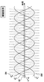
図9は、ダブルキャリア変調方式を説明するための図である。図9には、電圧指令値V*のゼロ値を示す基準軸(V*=0)が図示されている。交流電圧指令値V*
u、V*
v、V*
wと電圧指令値のゼロ値との交差点を「ゼロクロス」とも称す。図9には、「ゼロクロス付近領域X0」を表す破線枠が図示されている。
ゼロクロス付近領域X0は、交流電圧指令値のゼロクロス付近の領域である。ゼロクロス付近領域X0には、二つの三角波キャリア信号CW1、CW2それぞれの波形先端が並んでいる。三角波キャリア信号CW1、CW2の先端幅は狭いので、交流電圧指令値V*
u、V*
v、V*
wのゼロクロス付近においては、PWMパルスの幅が狭く生成される傾向がある。
狭すぎる幅のPWMパルスを生成しようとしても、そのような狭小なパルスはインバータ回路のデッドタイムによって消滅してしまうおそれがある。デッドタイムによるPWMパルス消滅が起きることで、電圧指令値のゼロクロス付近においてインバータ制御の制御性が低下しやすいという問題があった。
本出願は、上述のような課題を解決するためになされたもので、電圧指令値のゼロクロス付近で制御性が低下しないように改良された電力変換装置を提供することを目的とする。
本出願にかかる電力変換装置は、
複数の半導体スイッチング素子を含む三レベルインバータ回路と、
ダブルキャリア変調方式で前記三レベルインバータ回路を駆動するためのゲート信号を出力するインバータ制御回路と、
を備え、
前記インバータ制御回路は、
前記三レベルインバータ回路の出力電流と出力電圧とに基づいて、一つの交流電圧指令値と他の二つの交流電圧指令値とを含む三相出力電圧指令値を生成する指令値演算部と、
前記三相出力電圧指令値に補正を施した補正後指令値を出力する指令値補正部と、
前記補正後指令値に基づいて前記ゲート信号を生成するゲート信号生成部と、
を備え、
前記指令値補正部は、電圧指令値のゼロ値の周辺に予め定められた不感帯を前記一つの交流電圧指令値が通過する期間である不感帯通過期間には、前記一つの交流電圧指令値の代わりに前記不感帯の端に対応する所定電圧指令値を出力するとともに、前記不感帯通過期間における前記一つの交流電圧指令値と前記所定電圧指令値との差分を前記他の二つの交流電圧指令値に分配するように構築されたものである。
複数の半導体スイッチング素子を含む三レベルインバータ回路と、
ダブルキャリア変調方式で前記三レベルインバータ回路を駆動するためのゲート信号を出力するインバータ制御回路と、
を備え、
前記インバータ制御回路は、
前記三レベルインバータ回路の出力電流と出力電圧とに基づいて、一つの交流電圧指令値と他の二つの交流電圧指令値とを含む三相出力電圧指令値を生成する指令値演算部と、
前記三相出力電圧指令値に補正を施した補正後指令値を出力する指令値補正部と、
前記補正後指令値に基づいて前記ゲート信号を生成するゲート信号生成部と、
を備え、
前記指令値補正部は、電圧指令値のゼロ値の周辺に予め定められた不感帯を前記一つの交流電圧指令値が通過する期間である不感帯通過期間には、前記一つの交流電圧指令値の代わりに前記不感帯の端に対応する所定電圧指令値を出力するとともに、前記不感帯通過期間における前記一つの交流電圧指令値と前記所定電圧指令値との差分を前記他の二つの交流電圧指令値に分配するように構築されたものである。
本出願にかかる電力変換装置によれば、ゼロクロス付近に不感帯が設定されている。一つの交流電圧指令値がこの不感帯を通過するときには、ゼロクロス直近の小さな値が交流電圧指令値として設定されないように、交流電圧指令値に一定の制限を与えることができる。この制限により一つの交流電圧指令値が停滞した分は、他の二つの交流電圧指令値に分配することで、全体としてみれば適切な三相出力電圧指令値をインバータ回路に与えることができる。これにより、ゼロクロス付近での制御性が低下することを抑制することができる。
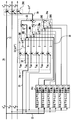
図1は、実施の形態にかかる電力変換装置1の構成を示す図である。電力変換装置1は、直流電源2からの直流電力を三相交流電力に変換する。電力変換装置1は、入力コンデンサC1,C2と三レベルインバータ回路10とインバータ制御回路20と変流器(CT)11と計器用変成器(VT)12とを備えている。
三レベルインバータ回路10は、複数の半導体スイッチング素子3を含んでいる。三レベルインバータ回路10は、中性点スイッチ方式のインバータ回路である。半導体スイッチング素子3は、絶縁ゲートバイポーラトランジスタ(IGBT)などの電力用半導体素子である。
三レベルインバータ回路10は、アーム回路を備えている。アーム回路は、複数の半導体スイッチング素子3が直列接続された回路である。
図1に示すように、直流電源2の正極出力と三レベルインバータ回路10のハイサイド母線とが接続されており、このハイサイド母線にはハイサイド電位V+が印加される。直流電源2の負極出力と三レベルインバータ回路10のローサイド母線とが接続されており、このローサイド母線にはローサイド電位V-が印加される。
入力コンデンサC1,C2からなる直列回路の一端は、上記のハイサイド母線に接続される。入力コンデンサC1,C2からなる直列回路の他端は、上記のローサイド母線に接続される。入力コンデンサC1と入力コンデンサC2との接続点から中性点電位V0が与えられる。
半導体スイッチング素子3の制御電極には、ゲート信号であるゲートパルスが印加される。ゲートパルスは、インバータ制御回路20で生成される。ゲートパルスは、パルス幅変調(PWM)パルスである。ゲートパルスによって、複数の半導体スイッチング素子3がオンオフ駆動する。
変流器11と計器用変成器12は、三レベルインバータ回路10の三相出力電流Iu、Iv、Iwと三相出力電圧Vu、Vv、Vwとを変換してインバータ制御回路20に伝達する。
インバータ制御回路20は、電力計算部21とフィードバック制御部22a、22bと電圧指令値V*を生成するインバータ電圧指令演算部23と指令値補正部24とゲート信号生成部25とを備えている。
実施の形態では、一例として、下記の計算ロジックに従って三相出力電圧指令値が算出される。電力計算部21は、複数の計器用変成器12の計測値および複数の変流器11の計測値に基づいて有効電力計測値と無効電力計測値とを計算する。インバータ制御回路20は、インバータ制御回路20の外部に設けられたインバータ電圧指令演算部(図示せず)から指令値を受け取る。指令値は、有効電力指令値P*と無効電力指令値Q*とを含んでいる。
有効電力差分ΔPが、第一の減算ブロックで演算される。有効電力差分ΔPは、電力計算部21からの有効電力計測値Pと有効電力指令値P*との差分である。無効電力差分ΔQが、第二の減算ブロックで演算される。無効電力差分ΔQは、電力計算部21からの無効電力計測値Qと無効電力指令値Q*との差分である。
フィードバック制御部22aは、有効電力差分ΔPに対して公知のフィードバック制御を実施する。フィードバック制御部22bは、無効電力差分ΔQに対して公知のフィードバック制御を実施する。それぞれのフィードバック制御は、PI制御とP制御とPID制御とのうち任意の一つを用いることができる。
インバータ電圧指令演算部23は、フィードバック制御部22aからの有効電力指令値とフィードバック制御部22bからの無効電力指令値とに基づいて三相電圧指令値を生成する。すなわち、インバータ電圧指令演算部23は、三レベルインバータ回路10の三相出力電流Iu、Iv、Iwと三相出力電圧Vu、Vv、Vwとに基づく電力計算部21と減算ブロックとフィードバック制御部22a、22bとによる一連の制御処理結果を受け取る。
この一連の制御処理結果に基づいて、インバータ電圧指令演算部23は三相出力電圧指令値V*
u1、V*
v1、V*
w1を生成する。
なお、上記のような有効電力および無効電力に基づく計算ロジックの代わりに、実施の形態の変形例としてMPPT((Maximum Power Point Tracking)制御に従って三相出力電圧指令値が設定されるようにインバータ制御回路20が構築されてもよい。このような変形例にかかるMPPT制御による三相出力電圧指令値の設定は、例えば直流電源2が太陽電池アレイである場合に用いることができる。
三相出力電圧指令値V*
u1、V*
v1、V*
w1は、第一相交流電圧指令値V*
u1と第二相交流電圧指令値V*
v1と第三相交流電圧指令値V*
w1とを含んでいる。
指令値補正部24は、三相出力電圧指令値V*
u1、V*
v1、V*
w1に補正を施した補正後指令値V*
u2、V*
v2、V*
w2を出力する。補正の内容を説明すると、まず、指令値補正部24は、不感帯通過期間TDBに、「不感帯DBを通過中の一つの交流電圧指令値」の代わりに不感帯DBの端に対応する所定電圧指令値VDBを出力する。
不感帯通過期間TDBは、不感帯DBを三相出力電圧指令値V*
u1、V*
v1、V*
w1のうち一つの交流電圧指令値が通過する期間である。不感帯DBは、電圧指令値V*のゼロ値(V*=0)の周辺に予め定められた指令値範囲である。不感帯DBの幅は、不感帯上限値VDBHと不感帯下限値VDBLとで決まる。不感帯上限値VDBHおよび不感帯下限値VDBLは不感帯DBのプラス端とマイナス端とを決める値であり、これらを所定電圧指令値VDBとも称す。
指令値補正部24は、不感帯通過期間TDBに、所定電圧指令値VDBを出力するとともに、差分ΔV*を「他の二つの交流電圧指令値」に分配する。「他の二つの交流電圧指令値」とは、三相出力電圧指令値V*
u1、V*
v1、V*
w1のうち、不感帯DBの外側に存在する二つの交流電圧指令値のことである。差分ΔV*は、不感帯通過期間TDBにおける、不感帯DBを通過中の一つの交流電圧指令値と所定電圧指令値VDBとの差分である。
これらの補正の結果、補正後指令値V*
u2、V*
v2、V*
w2が出力される。補正後指令値V*
u2、V*
v2、V*
w2は、補正後第一相交流電圧指令値V*
u2と補正後第二相交流電圧指令値V*
v2と補正後第三相交流電圧指令値V*
w2とを含んでいる。
図2は、実施の形態にかかる電力変換装置1が備える指令値補正部24の構成を示す図である。図3~図6は、実施の形態にかかる指令値補正部24の動作を説明するためのタイムチャートである。図3の上段に、三相出力電圧指令値V*
u1、V*
v1、V*
w1が図示されている。図3の下段に、補正後指令値V*
u2、V*
v2、V*
w2が図示されている。図3の中段には、補正に用いられる補正量ΔV*が図示されている。
図3から把握されるように、第一ゼロクロスzx1と第二ゼロクロスzx2と第三ゼロクロスzx3と第四ゼロクロスzx4と第五ゼロクロスzx5と第六ゼロクロスzx6とがこの順番で繰り返し到来する。
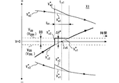
図4は、図3における時刻tx1の付近を指し示す破線部分X1を拡大したものである。図5は、図3における時刻tx2の付近を指し示す破線部分X2を拡大したものである。
以下、指令値補正部24の構成及び動作を説明する。以下の説明において、便宜上、「一つの交流電圧指令値」および「他の二つの交流電圧指令値」という用語を用いる。「一つの交流電圧指令値」とは、三相出力電圧指令値V*
u1、V*
v1、V*
w1のうちの任意の一つの交流電圧指令値を指している。
この「一つの交流電圧指令値」という用語は、主に、不感帯DBを通過する交流電圧指令値を、他の交流電圧指令値と区別するために用いられる。下記の説明では「一つの交流電圧指令値」に特定の相の交流電圧指令値を対応付けて説明することがあるが、「一つの交流電圧指令値」には三相出力電圧指令値V*
u1、V*
v1、V*
w1のいずれが代入されてもよい。
一方、「他の二つの交流電圧指令値」とは、三相出力電圧指令値V*
u1、V*
v1、V*
w1のうち上記一つの交流電圧指令値を除く残りの二つの一つの交流電圧指令値を指している。「他の二つの交流電圧指令値」という用語は、主に、不感帯DBの外側にある交流電圧指令値を参照するために用いられる。
図2に示すように、指令値補正部24は、補正量算出部24aと不感帯設定部24bと不感帯通過検出部24cと補正演算部24dとを含んでいる。
不感帯設定部24bは、不感帯DBの幅を設定するためのブロックである。不感帯DBは、図3~図6に記載されているように、電圧指令値V*のゼロ値(V*=0)の周辺に予め定められた範囲である。
不感帯設定部24bは、不感帯上限値VDBHと不感帯下限値VDBLとをそれぞれ設定変更可能に構築されている。実施の形態では、一例として、不感帯上限値VDBHと不感帯下限値VDBLとが、正負符号が逆であり且つ同じ大きさを持つように設定されている。その結果、指令値ゼロ(V*=0)を軸として不感帯DBはプラス側とマイナス側に同じ幅を持っている。
不感帯通過検出部24cは、不感帯通過期間TDBを検出する。不感帯通過期間TDBは、不感帯DBを一つの交流電圧指令値が通過する期間である。不感帯通過検出部24cは、不感帯DBに一つの交流電圧指令値が突入した時刻とこの一つの交流電圧指令値が不感帯DBを離脱した時刻との間の期間を不感帯通過期間TDBとして検出する。
図4には、補正動作の一例として、第二相交流電圧指令値V*
u1が不感帯DBをローサイド(マイナス側)からハイサイド(プラス側)へと通過する期間に実施される補正動作が図示されている。
図5には、一例として、第一相交流電圧指令値V*
u1が不感帯DBをハイサイド(プラス側)からローサイド(マイナス側)へと通過する期間に実施される補正動作が図示されている。
補正量算出部24aは、不感帯通過期間TDBにおいて、不感帯DBを通過中の一つの交流電圧指令値と所定電圧指令値VDBとの差分ΔV*を算出する。この差分ΔV*が、補正量ΔV*である。差分ΔV*の演算周期は、不感帯通過期間TDBに比べて十分に短いものとする。
所定電圧指令値VDBは、不感帯DBの端に対応する値である。実施の形態では、一例として、三相出力電圧指令値V*
u1、V*
v1、V*
w1それぞれが不感帯DBに突入する時に不感帯DBと交差する値を、三相出力電圧指令値V*
u1、V*
v1、V*
w1それぞれの所定電圧指令値VDBとして取り扱う。
すなわち、三相出力電圧指令値V*
u1、V*
v1、V*
w1それぞれがプラス側から不感帯DBに突入するときには、不感帯上限値VDBHが、補正量算出部24aで差分を算出するための所定電圧指令値VDBである。逆に、三相出力電圧指令値V*
u1、V*
v1、V*
w1それぞれがマイナス側から不感帯DBに突入するときには、不感帯下限値VDBLが、補正量算出部24aで差分を算出するための所定電圧指令値VDBである。
実施の形態では、図2に示すように、補正量算出部24aが、第一補正量算出ブロック24a1と第二補正量算出ブロック24a2と第三補正量算出ブロック24a3とを備える。
第一補正量算出ブロック24a1は、不感帯通過検出部24cで検出されたゼロクロス方向に応じて、第一相交流電圧指令値V*
u1と不感帯設定部24bの所定電圧指令値VDBとに基づいて、補正量ΔV*を算出する。補正量算出のための所定電圧指令値VDBには、具体的にはVDBHおよびVDBLのいずれか一つが選択的に使用される。
第二補正量算出ブロック24a2は、不感帯通過検出部24cで検出されたゼロクロス方向に応じて、第二相交流電圧指令値V*
v1と不感帯設定部24bの所定電圧指令値VDBとに基づいて、補正量ΔV*を算出する。第三補正量算出ブロック24a3は、不感帯通過検出部24cで検出されたゼロクロス方向に応じて、第三相交流電圧指令値V*
w1と不感帯設定部24bの所定電圧指令値VDBとに基づいて、補正量ΔV*を算出する。
補正演算部24dは、補正量ΔV*を三相出力電圧指令値V*
u1、V*
v1、V*
w1それぞれに加算する。補正演算部24dの加算によって、補正後指令値V*
u2、V*
v2、V*
w2それぞれが生成される。
上記の制御処理によれば、まず、指令値補正部24は、不感帯通過期間TDBには、補正量ΔV*の基礎となった一つの交流電圧指令値に対して補正量ΔV*を加算する。図4の例であれば、一つの交流電圧指令値V*
u1に対してΔV*が加算されている。この加算処理により、一つの交流電圧指令値が不感帯下限値VDBLに固定される。
従って、一つの交流電圧指令値の代わりに不感帯DBの端に対応する所定電圧指令値VDBが出力され、この所定電圧指令値VDBが補正後指令値V*
u2として取り扱われる。その結果、一つの交流電圧指令値の値が小さくなりすぎないようにゼロクロス付近で電圧指令値を不連続的に変化させることができる。
これに加えて、指令値補正部24は、不感帯通過期間TDBに、補正量ΔV*を他の二つの交流電圧指令値に加算する。図4の例では、補正量ΔV*が、他の二つの交流電圧指令値V*
v1、V*
w1に加算されている。この加算処理によって、差分ΔV*が他の二つの交流電圧指令値に分配され、分配後の指令値が補正後指令値として取り扱われる。他の二つの交流電圧指令値に対する指令値の分配によって、三相の相間電圧を保持することができる。
ゲート信号生成部25は、指令値補正部24からの補正後指令値V*
u2、V*
v2、V*
w2に基づいてゲート信号を生成する。ゲート信号は、三レベルインバータ回路10が持つ半導体スイッチング素子3のゲート駆動用PWM信号である。
ゲート信号生成部25は、デッドタイム生成部とキャリア信号生成部とPWM信号生成部とを含んでいる。
デッドタイム生成部について説明する。三レベルインバータ回路10が持つアーム回路にアーム短絡が発生することを防ぐために、デッドタイムが設けられている。デッドタイムは、アーム回路を構成するハイサイドの半導体スイッチング素子3とローサイドの半導体スイッチング素子3とのオンタイミングをずらすための遅延時間である。デッドタイムの長さによって、PWMパルスのターンオンエッジをどの程度遅延させるかが決定される。インバータ回路におけるデッドタイム設定技術は既に公知の技術であり、新規の事項ではないので、詳細な説明は省略する。
キャリア信号生成部について説明する。ゲート信号生成部25は、ダブルキャリア変調方式で三レベルインバータ回路10を駆動するためのゲート信号を出力する。ダブルキャリア変調方式では、レベルの異なる二つの三角波キャリア信号CW1、CW2が用いられる(図6参照)。ゲート信号生成部25は、これらの三角波キャリア信号CW1、CW2を出力するキャリア信号生成部(図示せず)を含んでいる。
図6に示すように、二つの三角波キャリア信号CW1、CW2は、ハイレベル三角波キャリア信号CW1とローレベル三角波キャリア信号CW2である。ハイレベル三角波キャリア信号CW1は、電圧指令値V*のゼロ値(V*=0)を基準として、プラスの値を取る搬送波である。ローレベル三角波キャリア信号CW2は、電圧指令値V*のゼロ値(V*=0)を基準として、マイナスの値を取る搬送波である。
PWM信号生成部について説明する。図6に示すように、補正後指令値V*
u2、V*
v2、V*
w2は、ハイレベル三角波キャリア信号CW1およびローレベル三角波キャリア信号CW2それぞれと交差する。補正後指令値V*
u2、V*
v2、V*
w2と各三角波キャリア信号CW1、CW2の交差点に基づいて、ゲートパルスの立ち上がりエッジおよび立ち下がりエッジが決定される。
一例として、補正後指令値V*
u2、V*
v2、V*
w2が三角波キャリア信号CW1、CW2を超えている期間にスイッチング素子を導通させるように、PWMゲートパルスが生成される。なお、電圧指令値と三角波キャリアとを比較してPWMパルスを作成する技術は、既に公知の技術であり新規の事項ではないので、PWM信号生成部についてのこれ以上の説明は省略する。
以上説明した実施の形態にかかる電力変換装置1は、下記の効果を奏する。三角波キャリア信号CW1、CW2の先端幅は狭いので、図9の関連技術で述べたように、交流電圧指令値V*
u、V*
v、V*
wのゼロクロス付近においてはPWMパルスの幅が狭く生成されるおそれがある。
この点、実施の形態にかかる電力変換装置1によれば、狭すぎる幅のPWMパルスが生成されることを抑制するために、電圧指令値のゼロクロス付近に不感帯DB(図3~図6参照)が設定されている。この不感帯DBに基づき不感帯通過期間TDBが検出される。不感帯通過期間TDBにおいては、ゼロクロス直近の小さな値が交流電圧指令値として設定されないように、補正量ΔV*の加算によって一つの交流電圧指令値に一定の制限が加えられる。一定の制限が加えられることで一つの交流電圧指令値が所定電圧指令値に保持されることとなる。この所定電圧指令値が補正後指令値V*
u2としてゲート信号生成部25で使用される。
これらの一連の制御処理によれば、ゼロクロス付近で交流電圧指令値の値に制限が加えられることで、インバータ回路のデッドタイムにより消滅するような狭小なパルスが生成されることを防止できる。その結果、電圧指令値のゼロクロス付近においてインバータ制御の制御性が低下することを抑制することができる。
また、実施の形態によれば、補正量ΔV*の加算によって一つの交流電圧指令値V*
u1が停滞した停滞分は、他の二つの交流電圧指令値V*
v1、V*
w1に分配される。分配後の値が補正後指令値V*
v2、V*
w2としてゲート信号生成部25で使用される。これにより、三相の相間電圧を適正に保つことができる。
このようにして、不感帯通過期間TDBにおいて三相出力電圧指令値V*
u1、V*
v1、V*
w1それぞれに補正が施されるものの、全体としてみれば適切な補正後指令値V*
u2、V*
v2、V*
w2をインバータ回路10に与えることができる。これにより、電圧指令値のゼロクロス付近での制御性が低下することを抑制することができる。これにより、例えば電圧指令値のゼロクロス付近における電流ひずみなどの問題を抑制することができる。
実施の形態では、指令値補正部24が不感帯DBを設定するための不感帯設定部24bを含むので、不感帯DBの幅を可変設定できるという利点がある。その結果、電圧指令値のゼロクロス付近での制御性低下を抑制するための必要十分な幅に、不感帯DBを設定できる利点がある。
実施の形態では、指令値補正部24が不感帯通過検出部24cを含むので、不感帯通過期間TDBを正確に検出できるという利点がある。
実施の形態では、指令値補正部24が補正量算出部24aと補正演算部24dとを含んでいる。これにより、一つの補正量ΔV*を演算してこれを三相出力電圧指令値V*
u1、V*
v1、V*
w1に加算することで、補正後指令値V*
u2、V*
v2、V*
w2を生成することができる。従って、複雑な演算処理を行わなくともよく、ハードウェア構成あるいはソフトウェア処理がシンプルになるという利点がある。
図7は、実施の形態にかかる電力変換装置1が備える指令値補正部24の具体的構成の一例を示す図である。図8は、実施の形態にかかる電力変換装置1が備える指令値補正部24の具体的構成の動作を説明するための図である。図7の指令値補正部24は、図2に記載した補正量算出部24aと不感帯設定部24bと不感帯通過検出部24cと補正演算部24dそれぞれの構成を具体化したものである。
不感帯通過検出部24cは、6つの検出ブロックで構築されている。第一検出ブロックは、第一相交流電圧指令値V*
u1が不感帯DBを上から下に通過中であるときに1を出力し、そうでないときに0を出力する。なお、ここで言及する「上」および「下」とは、図3~図6のタイミングチャートにおける紙面の上下に対応している。たとえば、電圧指令値が上から下に通過することは、電圧指令値がハイサイドからローサイドに不感帯DBを通過することを意味している。
第二検出ブロックは、第一相交流電圧指令値V*
u1が不感帯DBを下から上に通過中であるときに1を出力し、そうでないときに0を出力する。第三検出ブロックは、第二相交流電圧指令値V*
v1が不感帯DBを上から下に通過中であるときに1を出力し、そうでないときに0を出力する。
第四検出ブロックは、第二相交流電圧指令値V*
v1が不感帯DBを下から上に通過中であるときに1を出力し、そうでないときに0を出力する。第五検出ブロックは、第三相交流電圧指令値V*
w1が不感帯DBを上から下に通過中であるときに1を出力し、そうでないときに0を出力する。第六検出ブロックは、第三相交流電圧指令値V*
w1が不感帯DBを下から上に通過中であるときに1を出力し、そうでないときに0を出力する。
補正量算出部24aは、6つのスイッチSW1~SW6を備えている。第一スイッチSW1には、不感帯上限値VDBHと第一相交流電圧指令値V*
u1との第一差分値が入力されている。第一スイッチSW1は、第一検出ブロックの出力に応じて、第一差分値とゼロとの間で出力を切り替える。第一検出ブロックの出力が1であれば、第一スイッチSW1から第一差分値が出力される。第一検出ブロックの出力が0であれば、第一スイッチSW1からゼロが出力される。
第二スイッチSW2には、不感帯下限値VDBLと第一相交流電圧指令値V*
u1との第二差分値が入力されている。第二スイッチSW2は、第二検出ブロックの出力に応じて、第二差分値とゼロとの間で出力を切り替える。第二検出ブロックの出力が1であれば、第二スイッチSW2から第二差分値が出力される。第二検出ブロックの出力が0であれば、第二スイッチSW2からゼロが出力される。
第三スイッチSW3には、不感帯上限値VDBHと第二相交流電圧指令値V*
v1との第三差分値が入力されている。第三スイッチSW3は、第三検出ブロックの出力に応じて、第三差分値とゼロとの間で出力を切り替える。第三検出ブロックの出力が1であれば、第三スイッチSW3から第三差分値が出力される。第三検出ブロックの出力が0であれば、第三スイッチSW3からゼロが出力される。
第四スイッチSW4には、不感帯下限値VDBLと第二相交流電圧指令値V*
v1との第四差分値が入力されている。第四スイッチSW4は、第四検出ブロックの出力に応じて、第四差分値とゼロとの間で出力を切り替える。第四検出ブロックの出力が1であれば、第四スイッチSW4から第四差分値が出力される。第四検出ブロックの出力が0であれば、第四スイッチSW4からゼロが出力される。
第五スイッチSW5には、不感帯上限値VDBHと第三相交流電圧指令値V*
w1との第五差分値が入力されている。第五スイッチSW5は、第五検出ブロックの出力に応じて、第五差分値とゼロとの間で出力を切り替える。第五検出ブロックの出力が1であれば、第五スイッチSW5から第五差分値が出力される。第五検出ブロックの出力が0であれば、第五スイッチSW5からゼロが出力される。
第六スイッチSW6には、不感帯下限値VDBLと第三相交流電圧指令値V*
w1との第六差分値が入力されている。第六スイッチSW6は、第六検出ブロックの出力に応じて、第六差分値とゼロとの間で出力を切り替える。第六検出ブロックの出力が1であれば、第六スイッチSW6から第六差分値が出力される。第六検出ブロックの出力が0であれば、第六スイッチSW6からゼロが出力される。
補正量算出部24aは、第一スイッチSW1~第六スイッチSW6の合計値を出力する。ただし、図3から把握されるように、三相出力電圧指令値V*
u1、V*
v1、V*
w1それぞれのゼロクロスタイミングは互いに異なっている。
具体的には、図3から把握されるように、第一ゼロクロスzx1と第二ゼロクロスzx2と第三ゼロクロスzx3と第四ゼロクロスzx4と第五ゼロクロスzx5と第六ゼロクロスzx6とがこの順番で繰り返し到来する。
第一ゼロクロスzx1は、w相指令値が指令値ゼロを上から下に通過するゼロクロスである。第二ゼロクロスzx2は、v相指令値が指令値ゼロを下から上に通過するゼロクロスである。第三ゼロクロスzx3は、u相指令値が指令値ゼロを上から下に通過するゼロクロスである。
第四ゼロクロスzx4は、w相指令値が指令値ゼロを下から上に通過するゼロクロスである。第五ゼロクロスzx5は、v相指令値が指令値ゼロを上から下に通過するゼロクロスである。第六ゼロクロスzx6は、u相指令値が指令値ゼロを下から上に通過するゼロクロスである。
なお、「上から下」とは、プラス値からマイナス値へと向かう変化を意味している。「下から上」とは、マイナス値からプラス値へと向かう変化を意味している。
従って、ゼロ以外の差分値を出力するスイッチは、第五スイッチSW5、第四スイッチSW4、第一スイッチSW1、第六スイッチSW6、第三スイッチSW3、第二スイッチSW2、第五スイッチSW5、・・・という順番で交代していく。このように第一スイッチSW1~第六スイッチSW6のなかで一つのスイッチのみがゼロ以外の差分値を出力し、残りのスイッチがゼロを出力する。その結果、補正量算出部24aからは、上記の第一差分値から第六差分値のなかのいずれか一つの値が、選択的に差分値ΔV*として出力される。
補正量算出部24aが出力した差分値ΔV*は、補正演算部24dにおいて、三相出力電圧指令値V*
u1、V*
v1、V*
w1に加算される。
図8を用いて、図4に示すゼロクロスの場合における図7の回路動作を説明する。図4は、u相指令値が下から上に不感帯DBを通過するので、第六ゼロクロスzx6に対応している。まず、図8の信号S1として、第一相交流電圧指令値V*
u1が補正演算部24dに伝達される。これと同時に、図8の信号S2として、第一相交流電圧指令値V*
u1が不感帯通過検出部24cの第二ブロックに入力される。
さらに、図8の信号S3として、第一相交流電圧指令値V*
u1が補正量算出部24aへと入力される。また、不感帯設定部24bから、図8の信号S4である不感帯下限値VDBLが、補正量算出部24aへと入力される。
不感帯下限値VDBLと第一相交流電圧指令値V*
u1との差分が、補正量ΔV*として算出される。補正量ΔV*は、図8の信号S5である。
不感帯通過検出部24cの第二ブロックは、図8の信号S6として、1を出力する。信号S6は、補正量算出部24aの第二スイッチSW2をオンに切り替える。オンされた第二スイッチSW2は、補正量ΔV*を信号S7として出力する。
その後、信号S7は第一スイッチSW1の出力と加算されることで信号S8となり、この信号S8はさらに第三スイッチSW3~第六スイッチSW6の出力と合計されることで信号S9となる。信号S9は、補正量算出部24aの出力である。
前述したように、第二スイッチSW2が補正量ΔV*を算出しているときには、他のスイッチの出力は全てゼロである。従って、信号S9は、信号S5の値と一致する。補正演算部24dは、信号S9である補正量ΔV*を、三相出力電圧指令値V*
u1、V*
v1、V*
w1に加算する。
図10および図11は、実施の形態の変形例にかかる指令値補正部24の動作を説明するためのタイムチャートである。図10は、図4に示した時刻tx1付近の補正動作を変形させたものである。図11は、図5に示した時刻tx2付近の補正動作を変形させたものである。
図4、図5、図10および図11を関連付けて説明すると、指令値補正部24の補正動作バリエーションには、下記の表に示すように四つの種類が存在する。第一補正動作は、図4で説明したものである。第二補正動作は、図5で説明したものである。表1の「所定電圧指令値」は、不感帯DBを通過する交流電圧指令値が、不感帯通過期間TDBに貼り付く値である。
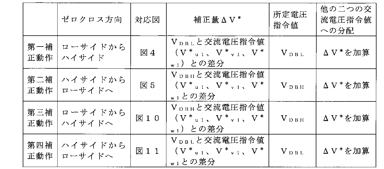
図10の第三補正動作におけるゼロクロス方向は、ローサイドからハイサイドへ向かう方向(つまり図中の下から上)なので、図4の第一補正動作と同じである。しかし、第三補正動作は、不感帯DBへの突入時に、不感帯DBへの突入端に当たる不感帯下限値VDBLではなく、不感帯DBの離脱点となる不感帯上限値VDBHを用いて、差分ΔV*を算出する。
図11の第四補正動作におけるゼロクロス方向は、ハイサイドからローサイドへ向かう方向(つまり図中の上から下)なので、図5の第二補正動作と同じである。しかし、第四補正動作は、不感帯DBへの突入時に、不感帯DBへの突入端に当たる不感帯上限値VDBHではなく、不感帯DBの離脱点となる不感帯下限値VDBLを用いて、差分ΔV*を算出する。
なお、上記第三補正動作および第四補正動作を実現するためには、図2および図7に示した指令値補正部24の回路ブロックにおいて、差分ΔV*を算出するロジックを変更すればよい。従って、詳細な回路説明は省略する。
指令値補正部24は、ローサイドからハイサイドへのゼロクロス方向について、第一補正動作と第三補正動作とのうち一方の補正動作を用いることができる。指令値補正部24は、ハイサイドからローサイドへのゼロクロス方向について、第二補正動作と第四補正動作とのうち一方の補正動作を用いることができる。
実施の形態では、指令値補正部24が、上記の第一補正動作と第二補正動作とを実行している。これに対し、変形例として、指令値補正部24が、上記第一補正動作と第四補正動作とを実行してもよい。あるいは、他の変形例として、指令値補正部24が、上記第二補正動作と第三補正動作とを実行してもよい。あるいは、他の変形例として、指令値補正部24が、上記第三補正動作と第四補正動作とを実行してもよい。また、さらなる変形例として、指令値補正部24が、上記第一~第四補正動作それぞれを実行可能に構築され、条件に応じてこれらを選択的に切り替えるように構築されてもよい。
なお、三レベルインバータ回路10の変形例として、中性点電位クランプ方式のインバータ回路が用いられてもよい。中性点電位クランプ方式のインバータ回路の一例は日本特開2001-136750号公報の図10に記載されており、中性点電位クランプ方式のインバータ回路構成は新規な事項ではない。従って、図示及び説明を省略する。
1 電力変換装置、2 直流電源、3 半導体スイッチング素子、10 インバータ回路(三レベルインバータ回路)、11 変流器(CT)、12 計器用変成器(VT)、20 インバータ制御回路、21 電力計算部、22a フィードバック制御部、22b フィードバック制御部、23 インバータ電圧指令演算部、24 指令値補正部、24a 補正量算出部、24a1 第一補正量算出ブロック、24a2 第二補正量算出ブロック、24a3 第三補正量算出ブロック、24b 不感帯設定部、24c 不感帯通過検出部、24d 補正演算部、25 ゲート信号生成部、C1、C2 入力コンデンサ、CW1 三角波キャリア信号(ハイレベル三角波キャリア信号)、CW2 三角波キャリア信号(ローレベル三角波キャリア信号)、DB 不感帯、Iu、Iv、Iw 三相出力電流、P 有効電力計測値、P* 有効電力指令値、Q 無効電力計測値、Q* 無効電力指令値、TDB 不感帯通過期間、V- ローサイド電位、V+ ハイサイド電位、V*
u1 三相出力電圧指令値(第一相交流電圧指令値)、V*
v1 三相出力電圧指令値(第二相交流電圧指令値)、V*
w1 三相出力電圧指令値(第三相交流電圧指令値)、V*
u2 補正後指令値(補正後第一相交流電圧指令値)、V*
v2 補正後指令値(補正後第三相交流電圧指令値)、V*
w2 補正後指令値(補正後第二相交流電圧指令値)、V0 中性点電位、VDB 所定電圧指令値、VDBH 不感帯上限値(所定電圧指令値)、VDBL 不感帯下限値(所定電圧指令値)、Vu、Vv、Vw 三相出力電圧、X0 ゼロクロス付近領域、zx1 第一ゼロクロス、zx2 第二ゼロクロス、zx3 第三ゼロクロス、zx4 第四ゼロクロス、zx5 第五ゼロクロス、zx6 第六ゼロクロス、ΔV* 差分(補正量)
Claims (4)
- 複数の半導体スイッチング素子を含む三レベルインバータ回路と、
ダブルキャリア変調方式で前記三レベルインバータ回路を駆動するためのゲート信号を出力するインバータ制御回路と、
を備え、
前記インバータ制御回路は、
前記三レベルインバータ回路の出力電流と出力電圧とに基づいて、一つの交流電圧指令値と他の二つの交流電圧指令値とを含む三相出力電圧指令値を生成する指令値演算部と、
前記三相出力電圧指令値に補正を施した補正後指令値を出力する指令値補正部と、
前記補正後指令値に基づいて前記ゲート信号を生成するゲート信号生成部と、
を備え、
前記指令値補正部は、電圧指令値のゼロ値の周辺に予め定められた不感帯を前記一つの交流電圧指令値が通過する期間である不感帯通過期間には、前記一つの交流電圧指令値の代わりに前記不感帯の端に対応する所定電圧指令値を出力するとともに、前記不感帯通過期間における前記一つの交流電圧指令値と前記所定電圧指令値との差分を前記他の二つの交流電圧指令値に分配するように構築された電力変換装置。 - 前記指令値補正部は、前記不感帯の幅を可変に設定可能な不感帯設定部を含む請求項1に記載の電力変換装置。
- 前記指令値補正部は、前記不感帯に前記一つの交流電圧指令値が突入した第一時刻と前記一つの交流電圧指令値が前記不感帯を離脱した第二時刻との間の期間を前記不感帯通過期間として検出する不感帯通過検出部を含む請求項1または2に記載の電力変換装置。
- 前記指令値補正部は、
前記不感帯通過期間における前記一つの交流電圧指令値と前記所定電圧指令値との前記差分を算出する補正量算出部と、
前記差分を前記一つの交流電圧指令値に加算することで前記一つの交流電圧指令値を前記所定電圧指令値に固定するとともに、前記差分を前記他の二つの交流電圧指令値に加算するように構築された補正演算部と、
を含む請求項1~3のいずれか1項に記載の電力変換装置。
Priority Applications (6)
| Application Number | Priority Date | Filing Date | Title |
|---|---|---|---|
| PCT/JP2019/024526 WO2020255338A1 (ja) | 2019-06-20 | 2019-06-20 | 電力変換装置 |
| ES19872259T ES2931151T3 (es) | 2019-06-20 | 2019-06-20 | Dispositivo de conversión de energía |
| EP19872259.7A EP3780377B1 (en) | 2019-06-20 | 2019-06-20 | Power conversion device |
| JP2020543836A JP6933306B2 (ja) | 2019-06-20 | 2019-06-20 | 電力変換装置 |
| US17/284,686 US11290003B2 (en) | 2019-06-20 | 2019-06-20 | Power conversion device |
| CN201980007382.1A CN112492892B (zh) | 2019-06-20 | 2019-06-20 | 电力变换装置 |
Applications Claiming Priority (1)
| Application Number | Priority Date | Filing Date | Title |
|---|---|---|---|
| PCT/JP2019/024526 WO2020255338A1 (ja) | 2019-06-20 | 2019-06-20 | 電力変換装置 |
Publications (1)
| Publication Number | Publication Date |
|---|---|
| WO2020255338A1 true WO2020255338A1 (ja) | 2020-12-24 |
Family
ID=74040420
Family Applications (1)
| Application Number | Title | Priority Date | Filing Date |
|---|---|---|---|
| PCT/JP2019/024526 Ceased WO2020255338A1 (ja) | 2019-06-20 | 2019-06-20 | 電力変換装置 |
Country Status (6)
| Country | Link |
|---|---|
| US (1) | US11290003B2 (ja) |
| EP (1) | EP3780377B1 (ja) |
| JP (1) | JP6933306B2 (ja) |
| CN (1) | CN112492892B (ja) |
| ES (1) | ES2931151T3 (ja) |
| WO (1) | WO2020255338A1 (ja) |
Families Citing this family (4)
| Publication number | Priority date | Publication date | Assignee | Title |
|---|---|---|---|---|
| CN111130369B (zh) * | 2019-12-31 | 2021-06-15 | 华为技术有限公司 | 一种逆变电路控制方法及相关装置 |
| JP7569265B2 (ja) * | 2021-05-12 | 2024-10-17 | 株式会社日立製作所 | インバータ制御装置、電力変換装置 |
| CN117882287A (zh) * | 2021-09-06 | 2024-04-12 | 三菱电机株式会社 | 电力变换器的控制部以及电力变换装置 |
| CN114759818B (zh) * | 2022-04-29 | 2025-05-16 | 深圳市英威腾电气股份有限公司 | 一种十三段式载波脉宽调制方法、系统及相关组件 |
Citations (4)
| Publication number | Priority date | Publication date | Assignee | Title |
|---|---|---|---|---|
| JP2001136750A (ja) | 1999-11-10 | 2001-05-18 | Yaskawa Electric Corp | 3レベルnpcインバータのpwmパルス発生回路 |
| JP2009225525A (ja) * | 2008-03-14 | 2009-10-01 | Daikin Ind Ltd | コンバータの制御方法及び制御装置 |
| JP2016032373A (ja) * | 2014-07-29 | 2016-03-07 | 株式会社日立製作所 | 3レベル三相インバータの駆動制御装置 |
| WO2018033964A1 (ja) * | 2016-08-16 | 2018-02-22 | 東芝三菱電機産業システム株式会社 | 系統連系インバータ装置及びその運転方法 |
Family Cites Families (13)
| Publication number | Priority date | Publication date | Assignee | Title |
|---|---|---|---|---|
| GB2238188B (en) * | 1989-05-16 | 1993-12-22 | Mitsubishi Electric Corp | Pulse-width modulation type inverter apparatus |
| JPH0352564A (ja) * | 1989-07-19 | 1991-03-06 | Hitachi Ltd | インバータの制御装置 |
| JP3222489B2 (ja) * | 1991-06-28 | 2001-10-29 | 株式会社東芝 | 3相3線式の中性点クランプ式インバータの制御方法 |
| US5206802A (en) * | 1991-09-17 | 1993-04-27 | Otis Elevator Company | Blanking interval voltage deviation compensator for inverters and converters |
| JPH0984360A (ja) * | 1995-09-19 | 1997-03-28 | Toshiba Corp | Npcインバータ装置 |
| JP3580048B2 (ja) * | 1996-10-03 | 2004-10-20 | 富士電機システムズ株式会社 | インバータのデッドタイム補償回路 |
| JP5277671B2 (ja) * | 2008-03-11 | 2013-08-28 | 株式会社リコー | モータ駆動装置 |
| JP5974646B2 (ja) * | 2012-06-07 | 2016-08-23 | 富士電機株式会社 | 3レベル電力変換回路の制御装置 |
| JP2018064322A (ja) * | 2016-10-11 | 2018-04-19 | 株式会社豊田自動織機 | 車両用インバータ駆動装置及び車両用流体機械 |
| US10951144B2 (en) * | 2017-06-21 | 2021-03-16 | Toshiba Mitsubishi-Electric Industrial Systems Corporation | Thyristor starter |
| EP3726686A4 (en) * | 2017-12-11 | 2021-10-06 | Toshiba Mitsubishi-Electric Industrial Systems Corporation | POWER CONVERSION DEVICE |
| JP6676830B1 (ja) * | 2018-11-21 | 2020-04-08 | 東芝三菱電機産業システム株式会社 | 電力変換装置 |
| CN111742280B (zh) * | 2019-01-21 | 2022-03-01 | 东芝三菱电机产业系统株式会社 | 电力转换装置及电力转换系统 |
-
2019
- 2019-06-20 US US17/284,686 patent/US11290003B2/en active Active
- 2019-06-20 ES ES19872259T patent/ES2931151T3/es active Active
- 2019-06-20 JP JP2020543836A patent/JP6933306B2/ja active Active
- 2019-06-20 EP EP19872259.7A patent/EP3780377B1/en active Active
- 2019-06-20 WO PCT/JP2019/024526 patent/WO2020255338A1/ja not_active Ceased
- 2019-06-20 CN CN201980007382.1A patent/CN112492892B/zh active Active
Patent Citations (4)
| Publication number | Priority date | Publication date | Assignee | Title |
|---|---|---|---|---|
| JP2001136750A (ja) | 1999-11-10 | 2001-05-18 | Yaskawa Electric Corp | 3レベルnpcインバータのpwmパルス発生回路 |
| JP2009225525A (ja) * | 2008-03-14 | 2009-10-01 | Daikin Ind Ltd | コンバータの制御方法及び制御装置 |
| JP2016032373A (ja) * | 2014-07-29 | 2016-03-07 | 株式会社日立製作所 | 3レベル三相インバータの駆動制御装置 |
| WO2018033964A1 (ja) * | 2016-08-16 | 2018-02-22 | 東芝三菱電機産業システム株式会社 | 系統連系インバータ装置及びその運転方法 |
Non-Patent Citations (1)
| Title |
|---|
| See also references of EP3780377A4 |
Also Published As
| Publication number | Publication date |
|---|---|
| ES2931151T3 (es) | 2022-12-27 |
| CN112492892A (zh) | 2021-03-12 |
| EP3780377A4 (en) | 2021-02-17 |
| JP6933306B2 (ja) | 2021-09-08 |
| EP3780377A1 (en) | 2021-02-17 |
| EP3780377B1 (en) | 2022-09-28 |
| JPWO2020255338A1 (ja) | 2021-09-13 |
| CN112492892B (zh) | 2023-08-04 |
| US11290003B2 (en) | 2022-03-29 |
| US20210359593A1 (en) | 2021-11-18 |
Similar Documents
| Publication | Publication Date | Title |
|---|---|---|
| JP6933306B2 (ja) | 電力変換装置 | |
| DE102011001171B4 (de) | Leistungswandler | |
| US8929111B2 (en) | System and method for common-mode elimination in a multi-level converter | |
| Banaei et al. | New multilevel inverter with reduction of switches and gate driver | |
| US7106025B1 (en) | Cancellation of dead time effects for reducing common mode voltages | |
| EP2412087B1 (en) | A power supply, method, and computer program product for supplying electrical power to a load | |
| CN105900328B (zh) | 功率转换装置 | |
| CN100574090C (zh) | 电功率转换设备 | |
| JP2017184309A (ja) | 電力変換装置 | |
| EP2493075A2 (en) | Current-source power converting apparatus | |
| US11848600B2 (en) | Power conversion device with control circuit to adjust a common mode voltage of combined output voltages | |
| US11646676B2 (en) | Method and apparatus for generating a three-phase voltage | |
| Lu et al. | Advanced control of cascaded multilevel drives based on PQ theory | |
| Jahmeerbacus et al. | Evaluation of Selective Harmonic Elimination and sinusoidal PWM for single-phase DC to AC inverters under dead-time distortion | |
| JP2019047701A (ja) | 電力変換装置およびその制御方法 | |
| Lee et al. | A novel control of three-phase PWM rectifier using single current sensor | |
| JP3248301B2 (ja) | Pwm制御インバータの制御回路 | |
| JP4277360B2 (ja) | 3レベルインバータの制御装置 | |
| Wang et al. | Real time simulation of a FPGA based space vector PWM controller | |
| CN113541569A (zh) | 电机驱动装置、方法、空调及计算机可读存储介质 | |
| JP2006166628A (ja) | 電力変換装置の制御方法 | |
| JPH09149658A (ja) | 直列多重型インバータ装置 | |
| Cha et al. | An approach to reduce common mode voltage in matrix converter | |
| JP3615966B2 (ja) | 系統連係インバータ装置 | |
| WO2024105841A1 (ja) | 電力変換装置、および飛行物体 |
Legal Events
| Date | Code | Title | Description |
|---|---|---|---|
| ENP | Entry into the national phase |
Ref document number: 2019872259 Country of ref document: EP Effective date: 20200422 |
|
| ENP | Entry into the national phase |
Ref document number: 2020543836 Country of ref document: JP Kind code of ref document: A |
|
| NENP | Non-entry into the national phase |
Ref country code: DE |