WO2020255376A1 - 複合基板の製造方法、および、複合基板 - Google Patents
複合基板の製造方法、および、複合基板 Download PDFInfo
- Publication number
- WO2020255376A1 WO2020255376A1 PCT/JP2019/024725 JP2019024725W WO2020255376A1 WO 2020255376 A1 WO2020255376 A1 WO 2020255376A1 JP 2019024725 W JP2019024725 W JP 2019024725W WO 2020255376 A1 WO2020255376 A1 WO 2020255376A1
- Authority
- WO
- WIPO (PCT)
- Prior art keywords
- substrate
- composite substrate
- diamond
- gan
- recess
- Prior art date
- Legal status (The legal status is an assumption and is not a legal conclusion. Google has not performed a legal analysis and makes no representation as to the accuracy of the status listed.)
- Ceased
Links
Images













Classifications
-
- H—ELECTRICITY
- H10—SEMICONDUCTOR DEVICES; ELECTRIC SOLID-STATE DEVICES NOT OTHERWISE PROVIDED FOR
- H10P—GENERIC PROCESSES OR APPARATUS FOR THE MANUFACTURE OR TREATMENT OF DEVICES COVERED BY CLASS H10
- H10P10/00—Bonding of wafers, substrates or parts of devices
- H10P10/12—Bonding of semiconductor wafers or semiconductor substrates to semiconductor wafers or semiconductor substrates
-
- B—PERFORMING OPERATIONS; TRANSPORTING
- B23—MACHINE TOOLS; METAL-WORKING NOT OTHERWISE PROVIDED FOR
- B23K—SOLDERING OR UNSOLDERING; WELDING; CLADDING OR PLATING BY SOLDERING OR WELDING; CUTTING BY APPLYING HEAT LOCALLY, e.g. FLAME CUTTING; WORKING BY LASER BEAM
- B23K10/00—Welding or cutting by means of a plasma
- B23K10/02—Plasma welding
-
- H—ELECTRICITY
- H10—SEMICONDUCTOR DEVICES; ELECTRIC SOLID-STATE DEVICES NOT OTHERWISE PROVIDED FOR
- H10W—GENERIC PACKAGES, INTERCONNECTIONS, CONNECTORS OR OTHER CONSTRUCTIONAL DETAILS OF DEVICES COVERED BY CLASS H10
- H10W10/00—Isolation regions in semiconductor bodies between components of integrated devices
- H10W10/01—Manufacture or treatment
- H10W10/021—Manufacture or treatment of air gaps
-
- B—PERFORMING OPERATIONS; TRANSPORTING
- B23—MACHINE TOOLS; METAL-WORKING NOT OTHERWISE PROVIDED FOR
- B23K—SOLDERING OR UNSOLDERING; WELDING; CLADDING OR PLATING BY SOLDERING OR WELDING; CUTTING BY APPLYING HEAT LOCALLY, e.g. FLAME CUTTING; WORKING BY LASER BEAM
- B23K15/00—Electron-beam welding or cutting
- B23K15/0006—Electron-beam welding or cutting specially adapted for particular articles or work
-
- B—PERFORMING OPERATIONS; TRANSPORTING
- B23—MACHINE TOOLS; METAL-WORKING NOT OTHERWISE PROVIDED FOR
- B23K—SOLDERING OR UNSOLDERING; WELDING; CLADDING OR PLATING BY SOLDERING OR WELDING; CUTTING BY APPLYING HEAT LOCALLY, e.g. FLAME CUTTING; WORKING BY LASER BEAM
- B23K15/00—Electron-beam welding or cutting
- B23K15/0046—Welding
-
- B—PERFORMING OPERATIONS; TRANSPORTING
- B23—MACHINE TOOLS; METAL-WORKING NOT OTHERWISE PROVIDED FOR
- B23K—SOLDERING OR UNSOLDERING; WELDING; CLADDING OR PLATING BY SOLDERING OR WELDING; CUTTING BY APPLYING HEAT LOCALLY, e.g. FLAME CUTTING; WORKING BY LASER BEAM
- B23K20/00—Non-electric welding by applying impact or other pressure, with or without the application of heat, e.g. cladding or plating
- B23K20/20—Special methods allowing subsequent separation, e.g. of metals of high quality from scrap material
-
- H—ELECTRICITY
- H10—SEMICONDUCTOR DEVICES; ELECTRIC SOLID-STATE DEVICES NOT OTHERWISE PROVIDED FOR
- H10D—INORGANIC ELECTRIC SEMICONDUCTOR DEVICES
- H10D30/00—Field-effect transistors [FET]
- H10D30/40—FETs having zero-dimensional [0D], one-dimensional [1D] or two-dimensional [2D] charge carrier gas channels
- H10D30/47—FETs having zero-dimensional [0D], one-dimensional [1D] or two-dimensional [2D] charge carrier gas channels having two-dimensional [2D] charge carrier gas channels, e.g. nanoribbon FETs or high electron mobility transistors [HEMT]
-
- H—ELECTRICITY
- H10—SEMICONDUCTOR DEVICES; ELECTRIC SOLID-STATE DEVICES NOT OTHERWISE PROVIDED FOR
- H10H—INORGANIC LIGHT-EMITTING SEMICONDUCTOR DEVICES HAVING POTENTIAL BARRIERS
- H10H20/00—Individual inorganic light-emitting semiconductor devices having potential barriers, e.g. light-emitting diodes [LED]
- H10H20/01—Manufacture or treatment
- H10H20/011—Manufacture or treatment of bodies, e.g. forming semiconductor layers
- H10H20/018—Bonding of wafers
-
- H—ELECTRICITY
- H10—SEMICONDUCTOR DEVICES; ELECTRIC SOLID-STATE DEVICES NOT OTHERWISE PROVIDED FOR
- H10P—GENERIC PROCESSES OR APPARATUS FOR THE MANUFACTURE OR TREATMENT OF DEVICES COVERED BY CLASS H10
- H10P90/00—Preparation of wafers not covered by a single main group of this subclass, e.g. wafer reinforcement
-
- H—ELECTRICITY
- H10—SEMICONDUCTOR DEVICES; ELECTRIC SOLID-STATE DEVICES NOT OTHERWISE PROVIDED FOR
- H10P—GENERIC PROCESSES OR APPARATUS FOR THE MANUFACTURE OR TREATMENT OF DEVICES COVERED BY CLASS H10
- H10P90/00—Preparation of wafers not covered by a single main group of this subclass, e.g. wafer reinforcement
- H10P90/19—Preparing inhomogeneous wafers
- H10P90/1904—Preparing vertically inhomogeneous wafers
- H10P90/1906—Preparing SOI wafers
- H10P90/1914—Preparing SOI wafers using bonding
-
- H—ELECTRICITY
- H10—SEMICONDUCTOR DEVICES; ELECTRIC SOLID-STATE DEVICES NOT OTHERWISE PROVIDED FOR
- H10P—GENERIC PROCESSES OR APPARATUS FOR THE MANUFACTURE OR TREATMENT OF DEVICES COVERED BY CLASS H10
- H10P95/00—Generic processes or apparatus for manufacture or treatments not covered by the other groups of this subclass
- H10P95/11—Separation of active layers from substrates
-
- H—ELECTRICITY
- H10—SEMICONDUCTOR DEVICES; ELECTRIC SOLID-STATE DEVICES NOT OTHERWISE PROVIDED FOR
- H10W—GENERIC PACKAGES, INTERCONNECTIONS, CONNECTORS OR OTHER CONSTRUCTIONAL DETAILS OF DEVICES COVERED BY CLASS H10
- H10W10/00—Isolation regions in semiconductor bodies between components of integrated devices
- H10W10/20—Air gaps
-
- B—PERFORMING OPERATIONS; TRANSPORTING
- B23—MACHINE TOOLS; METAL-WORKING NOT OTHERWISE PROVIDED FOR
- B23K—SOLDERING OR UNSOLDERING; WELDING; CLADDING OR PLATING BY SOLDERING OR WELDING; CUTTING BY APPLYING HEAT LOCALLY, e.g. FLAME CUTTING; WORKING BY LASER BEAM
- B23K2101/00—Articles made by soldering, welding or cutting
- B23K2101/36—Electric or electronic devices
-
- B—PERFORMING OPERATIONS; TRANSPORTING
- B23—MACHINE TOOLS; METAL-WORKING NOT OTHERWISE PROVIDED FOR
- B23K—SOLDERING OR UNSOLDERING; WELDING; CLADDING OR PLATING BY SOLDERING OR WELDING; CUTTING BY APPLYING HEAT LOCALLY, e.g. FLAME CUTTING; WORKING BY LASER BEAM
- B23K2103/00—Materials to be soldered, welded or cut
- B23K2103/16—Composite materials
-
- H—ELECTRICITY
- H10—SEMICONDUCTOR DEVICES; ELECTRIC SOLID-STATE DEVICES NOT OTHERWISE PROVIDED FOR
- H10D—INORGANIC ELECTRIC SEMICONDUCTOR DEVICES
- H10D30/00—Field-effect transistors [FET]
- H10D30/40—FETs having zero-dimensional [0D], one-dimensional [1D] or two-dimensional [2D] charge carrier gas channels
- H10D30/47—FETs having zero-dimensional [0D], one-dimensional [1D] or two-dimensional [2D] charge carrier gas channels having two-dimensional [2D] charge carrier gas channels, e.g. nanoribbon FETs or high electron mobility transistors [HEMT]
- H10D30/471—High electron mobility transistors [HEMT] or high hole mobility transistors [HHMT]
- H10D30/475—High electron mobility transistors [HEMT] or high hole mobility transistors [HHMT] having wider bandgap layer formed on top of lower bandgap active layer, e.g. undoped barrier HEMTs such as i-AlGaN/GaN HEMTs
-
- H—ELECTRICITY
- H10—SEMICONDUCTOR DEVICES; ELECTRIC SOLID-STATE DEVICES NOT OTHERWISE PROVIDED FOR
- H10D—INORGANIC ELECTRIC SEMICONDUCTOR DEVICES
- H10D62/00—Semiconductor bodies, or regions thereof, of devices having potential barriers
- H10D62/80—Semiconductor bodies, or regions thereof, of devices having potential barriers characterised by the materials
- H10D62/85—Semiconductor bodies, or regions thereof, of devices having potential barriers characterised by the materials being Group III-V materials, e.g. GaAs
- H10D62/8503—Nitride Group III-V materials, e.g. AlN or GaN
-
- H—ELECTRICITY
- H10—SEMICONDUCTOR DEVICES; ELECTRIC SOLID-STATE DEVICES NOT OTHERWISE PROVIDED FOR
- H10P—GENERIC PROCESSES OR APPARATUS FOR THE MANUFACTURE OR TREATMENT OF DEVICES COVERED BY CLASS H10
- H10P50/00—Etching of wafers, substrates or parts of devices
- H10P50/20—Dry etching; Plasma etching; Reactive-ion etching
- H10P50/24—Dry etching; Plasma etching; Reactive-ion etching of semiconductor materials
- H10P50/242—Dry etching; Plasma etching; Reactive-ion etching of semiconductor materials of Group IV materials
-
- H—ELECTRICITY
- H10—SEMICONDUCTOR DEVICES; ELECTRIC SOLID-STATE DEVICES NOT OTHERWISE PROVIDED FOR
- H10P—GENERIC PROCESSES OR APPARATUS FOR THE MANUFACTURE OR TREATMENT OF DEVICES COVERED BY CLASS H10
- H10P50/00—Etching of wafers, substrates or parts of devices
- H10P50/20—Dry etching; Plasma etching; Reactive-ion etching
- H10P50/28—Dry etching; Plasma etching; Reactive-ion etching of insulating materials
- H10P50/282—Dry etching; Plasma etching; Reactive-ion etching of insulating materials of inorganic materials
- H10P50/283—Dry etching; Plasma etching; Reactive-ion etching of insulating materials of inorganic materials by chemical means
-
- H—ELECTRICITY
- H10—SEMICONDUCTOR DEVICES; ELECTRIC SOLID-STATE DEVICES NOT OTHERWISE PROVIDED FOR
- H10P—GENERIC PROCESSES OR APPARATUS FOR THE MANUFACTURE OR TREATMENT OF DEVICES COVERED BY CLASS H10
- H10P50/00—Etching of wafers, substrates or parts of devices
- H10P50/69—Etching of wafers, substrates or parts of devices using masks for semiconductor materials
- H10P50/691—Etching of wafers, substrates or parts of devices using masks for semiconductor materials for Group IV materials or Group III-V materials
- H10P50/693—Etching of wafers, substrates or parts of devices using masks for semiconductor materials for Group IV materials or Group III-V materials characterised by their size, orientation, disposition, behaviour or shape, in horizontal or vertical plane
Definitions
- the techniques disclosed in the specification of the present application relate to a method for manufacturing a composite substrate and a composite substrate.
- HEMT high electron mobility transistor
- GaN gallium nitride
- an inorganic adhesive is applied to a thin and curved polycrystalline diamond substrate in order to apply a transistor manufacturing process such as film formation, photoengraving or etching. Use to attach the supporting diamond substrate. Then, the polycrystalline diamond substrate and the supporting diamond substrate form a flat composite substrate having an appropriate thickness.
- the composite substrate is immersed in a chemical solution capable of dissolving an inorganic adhesive.
- the supporting diamond substrate may inadvertently peel off from the GaN-on-diamond substrate due to the penetration of the chemical solution into the inorganic adhesive, and the transistor is stably manufactured. The process cannot be carried out.
- the technique disclosed in the present specification has been made in view of the problems described above, and it is easy to remove each substrate in the composite substrate, and the composite substrate is peeled off in an unintended process.
- the purpose is to provide a technique for suppressing.
- a first aspect of the technique disclosed in the present specification is to form a first bonding material on a first surface of a first substrate, and on the first surface, a plane of the first substrate. At least one recess located inside the outer edge in the visual view is formed, and the first joining material is formed along the inner wall of the recess and fills the space surrounded by the inner wall of the recess. Instead, a second bonding material is formed on the second surface of the second substrate, and the first bonding material and the second bonding material are bonded in a region other than the recess.
- a second aspect of the technique disclosed herein is a first substrate having a first surface, a second substrate having a second surface, and a first surface formed on the first surface.
- the first surface is provided with a second bonding material formed on the second surface and bonded to the first bonding material, and the first surface is a flat surface of the first substrate.
- At least one recess located inside the outer edge in the visual view is formed, the first bonding material is formed along the inner wall of the recess, and the space surrounded by the inner wall of the recess is filled.
- the first joining material and the second joining material are joined in a region other than the recess.
- a first aspect of the technique disclosed in the present specification is to form a first bonding material on a first surface of a first substrate, and on the first surface, a plane of the first substrate. At least one recess located inside the outer edge in the visual view is formed, and the first joining material is formed along the inner wall of the recess and fills the space surrounded by the inner wall of the recess. Instead, a second bonding material is formed on the second surface of the second substrate, and the first bonding material and the second bonding material are bonded in a region other than the recess.
- the dissolution liquid penetrates into the space surrounded by the inner wall of the recess, so that the first and second bonding materials are dissolved faster, so that the time required for removing the first substrate is shortened. be able to. Further, since the dent is formed inside the outer edge portion, the first and second bonding materials are melted in an unintended step, and it is possible to prevent the composite substrate from peeling off.
- a second aspect of the technique disclosed herein is formed on a first substrate having a first surface, a second substrate having a second surface, and the first surface.
- a first bonding material and a second bonding material formed on the second surface and bonded to the first bonding material are provided, and the first surface is covered with the first substrate.
- At least one recess located inside the outer edge of the recess is formed, and the first bonding material is formed along the inner wall of the recess and in a space surrounded by the inner wall of the recess. Is not filled, and the first bonding material and the second bonding material are bonded in a region excluding the recess.
- the dissolution liquid penetrates into the space surrounded by the inner wall of the recess, so that the first and second bonding materials are dissolved faster, so that the time required for removing the first substrate is shortened. be able to. Further, since the dent is formed inside the outer edge portion, the first and second bonding materials are melted in an unintended step, and it is possible to prevent the composite substrate from peeling off.
- FIG. 3 is an enlarged plan view of region B in FIG.
- the upper surface of " or “the lower surface of " in addition to the upper surface of the target component itself, another upper surface of the target component may be used. It shall also include the state in which the components are formed. That is, for example, when the description "B provided on the upper surface of the instep” is described, it does not prevent another component " ⁇ " from intervening between the instep and the second.
- HEMT which has been put into practical use as a high-output and high-frequency transistor
- a high withstand voltage can be realized by using GaN as an active layer, and a low resistance can be realized by using a HEMT structure. Therefore, the above-mentioned HEMT can input a large amount of electric power.
- element destruction may occur due to Joule heat generated in the transistor section when a large amount of power is applied.
- a heat-dissipating member called a heat sink is mounted on a high-output transistor, but since the heat-generating part is limited to a minute area in the transistor, heat transport from the minute heat-generating part to the heat sink becomes an issue.
- the GaN film on which the transistor is formed is adhered to the heat sink with a base material such as a SiC (silicon carbide) substrate sandwiched between them.
- a base material such as a SiC (silicon carbide) substrate sandwiched between them.
- diamond having a higher thermal conductivity is used as a base material instead of SiC.
- the heat generated in the minute region of the GaN film diffuses the diamond layer in the lateral direction. Then, heat is transferred to a wide area of the heat sink that is adhered to the GaN film with the diamond substrate sandwiched between them, and as a result, the ultimate temperature at the heat generating portion can be lowered.
- a GaN thin film is crystal-grown on the upper surface of the Si substrate or the upper surface of the SiC substrate, and a support substrate is further adhered to the upper surface of the GaN thin film. After that, the Si substrate or the SiC substrate is removed.
- a protective film such as a silicon nitride (SiN) film on the lower surface of the GaN thin film exposed as a result
- a polycrystalline diamond layer is formed by a chemical vapor deposition, that is, CVD) method. ..
- GaN-on-diamond substrate a substrate in which a GaN thin film is formed on the upper surface of a polycrystalline diamond substrate.
- a diamond-based GaN transistor When a diamond-based GaN transistor is used, it is supported by an inorganic adhesive on a thin and curved polycrystalline diamond substrate in order to apply transistor fabrication processes such as film formation, photoengraving, or etching. Paste the diamond substrate. Then, the polycrystalline diamond substrate and the supporting diamond substrate form a flat composite substrate having an appropriate thickness.
- the polycrystalline diamond layer can be formed thickly by the CVD method, it is not necessary to separately attach the supporting diamond substrate as described above, and the transistor manufacturing process can be applied as it is.
- the substrate curvature in the film forming process becomes large, and the transistor manufacturing process cannot be applied.
- the thickness of the polycrystalline diamond layer must be the minimum thickness that functions as a heat transport material, for example, about 100 ⁇ m, and therefore, a supporting diamond substrate may be attached to form a composite substrate. You will need it.
- the composite substrate manufactured as described above has a coefficient of thermal expansion close to that of the GaN-on-diamond substrate and the supporting diamond substrate constituting the composite substrate in order to prevent bending in the thermal process of the transistor manufacturing process. It is necessary to select the material to have.
- a separately manufactured diamond substrate is used as the support substrate. Further, as a method for attaching the support substrate, it is necessary to select a method in which the structure after attachment has heat resistance. For example, attachment using an inorganic adhesive is performed.
- the GaN-on-diamond substrate has a thin thickness of about 100 ⁇ m, a mechanical method cannot be used to remove the supporting diamond substrate in order to prevent the substrate from being damaged.
- the supporting diamond substrate is removed from the GaN-on-diamond substrate by immersing the composite substrate in the chemical solution and further infiltrating the chemical solution into the porous inorganic adhesive.
- the composite substrate is immersed in a chemical solution capable of dissolving the inorganic adhesive.
- the supporting diamond substrate may inadvertently peel off from the GaN-on-diamond substrate due to the penetration of the chemical solution into the inorganic adhesive, and the transistor is stably manufactured. The process cannot be carried out.
- FIG. 1 is a perspective view showing an example of the configuration of the composite substrate according to the present embodiment.
- the composite substrate 1 includes a GaN-on-diamond substrate 2 and a supporting diamond substrate 3.
- FIG. 2 is a cross-sectional view showing a cross section taken along the line AA'in FIG.
- a SiO 2 bonding layer 22 and a SiO 2 bonding layer 40A are formed on the bonding surface between the GaN-on-diamond substrate 2 and the supporting diamond substrate 3. Further, a space 43A is formed between these bonding layers.
- the cross-sectional shape of the SiO 2 bonding layer 40A and the cross-sectional shape of the space 43A are not limited to those shown in FIG. 2, and for example, as will be described later, a recess on the upper surface of the supporting diamond substrate 3
- the side surface may have a curved surface shape, and the SiO 2 bonding layer formed on the side surface may also have a curved surface shape.
- FIG. 3 is a diagram showing an example of a semiconductor substrate and a support substrate constituting the composite substrate according to the present embodiment. As an example is shown in FIG. 3, a processing recess 35 is formed on the joint surface of the support diamond substrate 3 with the GaN on diamond substrate 2.
- FIG. 4 is an enlarged plan view of region B in FIG.
- the processing recess 35 is interrupted without reaching the outer edge portion 10 of the support diamond substrate 3, and the space inside the processing recess 35 is divided into the support diamond substrate 3 and the GaN on diamond substrate 2. It is closed in the joint surface between.
- the manufacturing process of the composite substrate in the present embodiment is roughly divided into the following four steps, that is, a step of preparing a GaN on diamond substrate, a step of preparing a supporting diamond substrate, a step of manufacturing a composite substrate, and a GaN. It consists of a process of forming an on-diamond transistor.
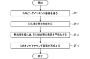
- FIG. 5 is a flowchart showing the process of preparing the GaN-on-diamond substrate among the above.
- FIG. 6 is a flowchart showing the process of preparing the supporting diamond substrate among the above.
- FIG. 7 is a flowchart showing the process of manufacturing the composite substrate among the above.
- FIG. 8 is a flowchart showing the process of forming the GaN on-diamond transistor among the above.
- the composite substrate according to the present embodiment is completed through the steps of producing the composite substrate shown in FIG. 7. Further, the step of forming the GaN-on-diamond transistor shown in FIG. 8 is merely a description of the latter half step of using the composite substrate according to the present embodiment.
- FIGS. 9, 10, 11, 12, and 13 are cross-sectional views showing an example of a state in the middle of the process of preparing the GaN on-diamond substrate.
- a GaN-on-Si substrate 15 as shown in FIG. 9 is manufactured.
- a buffer layer 12 made of an AlN (aluminum nitride) film or an AlGaN (gallium nitride aluminum) film, a GaN film 13, and an AlGaN film 14 are continuously connected to a 2-inch Si substrate 11 in that order. Epitaxially grow to.
- composition ratio of the buffer layer 12 is such that the lattice mismatch between the Si substrate 11 in contact with the lower surface and the GaN film 13 in contact with the upper surface is alleviated, and the stress contained in the GaN film 13 is alleviated.
- the film thickness etc. are adjusted.
- the buffer layer 12 may be a single layer, or may be formed by laminating a plurality of layers having different composition ratios.
- the thickness of the buffer layer 12 is, for example, 0.7 ⁇ m.
- the AlGaN film 14 is continuously epitaxially grown on the upper surface of the GaN film 13, and is two-dimensionally near the interface between the AlGaN film 14 in the GaN film 13 due to the spontaneous polarization effect and the piezo polarization effect of AlGaN. It generates a high-concentration electron layer called electron gas.
- this electron layer is less susceptible to ion scattering and exhibits extremely high electron mobility.
- a cap layer made of a GaN film may be formed on the upper surface of the AlGaN film 14, and impurities such as Fe or C (carbon) may be formed on a part of the GaN film 13. In some cases, a layer to which is added is sandwiched. In this way, the GaN-on-Si substrate 15 is manufactured.
- a support substrate adhesive layer 16 is formed on the upper surface of the AlGaN film 14 of the GaN-on-Si substrate 15. Then, the support substrate 17 is further adhered to the upper surface of the support substrate adhesive layer 16.
- the GaN transfer substrate 18 is obtained by removing the Si substrate 11 and the buffer layer 12.
- the support substrate adhesive layer 16 and the support substrate 17 need to have high temperature resistance.
- a laminated film of a SiN film and a SiO 2 film is applied as the support substrate adhesive layer 16.
- the SiN film by arranging the SiN film on the side closer to the AlGaN film 14, there is an effect of suppressing the release of nitrogen (N) from the AlGaN film 14 or the GaN film 13 in the high temperature step.
- the SiO 2 film in the laminated film as the support substrate adhesive layer 16 has an effect of realizing strong adhesion to the support substrate 17.
- the SiO 2 film is formed with a film thickness of, for example, 1.5 ⁇ m by a CVD method using TEOS (tetraethoxysilane). Then, for example, an annealing treatment is performed at 700 ° C., and a surface flattening treatment is further performed. Then, it is directly bonded to the Si substrate which is the support substrate 17 by a direct joining method.
- an inorganic adhesive containing alumina or silica as a main component can also be used.
- the GaN transfer substrate 18 is produced by removing the Si substrate 11 and the buffer layer 12, and the Si substrate 11 can be removed by, for example, mechanical polishing.
- the buffer layer 12 made of AlGaN or the like has a very slow mechanical polishing rate.
- the polishing conditions are changed for AlGaN polishing, and the buffer layer 12 is removed by polishing at a low speed. Then, the GaN film 13 is exposed.
- mechanical polishing is used for removing the Si substrate 11 and the buffer layer 12, but vapor phase etching can also be used by reactive ion etching (that is, RIE) method. Since only the surface to be processed is removed in both the mechanical polishing and the RIE method, the Si substrate 11 is removed in a state where the support substrate 17 which is a Si substrate is also arranged on the opposite surface as in the present embodiment. Is suitable for.
- a chemical treatment such as fluorine can be applied to the removal of the Si substrate 11. If the chemical treatment can be used, the ratio of the removal rate between the Si substrate 11 and the buffer layer 12 (that is, the selection ratio) becomes very large, so that the removal can be reliably stopped when the buffer layer 12 is exposed. it can.
- a laminated film of a SiN film and a SiO 2 film is used as the support substrate adhesive layer 16, but the material is not limited to this, and other film types may be used.
- An inorganic adhesive containing alumina or silica as a main component may be used.
- a protective layer 19 is formed on the lower surface of the GaN film 13 of the GaN transfer substrate 18.
- the polycrystalline diamond film-forming substrate 21 is produced by forming the polycrystalline diamond film 20 on the lower surface of the protective layer 19.
- the protective layer 19 is to protect the GaN film 13 with the protective layer 19 when the polycrystalline diamond film 20 is formed.
- the protective layer 19 is an amorphous Si thin film, and is formed by, for example, a plasma CVD method.
- the film thickness of the protective layer 19 is as much as necessary to protect the GaN film 13, but if the film thickness of the protective layer 19 is too thick, the protective layer 19 becomes the GaN film 13 and the polycrystalline diamond film. It interferes with heat conduction with 20.
- amorphous Si having a film thickness of 20 nm is formed as the protective layer 19.
- the protective layer 19 is not limited to the case of amorphous Si, and may be another film type. If the damage of the GaN film 13 can be ignored, the protective layer 19 is not formed. May be good.
- a microwave plasma CVD method using methane gas and hydrogen is applied for the formation of the polycrystalline diamond film 20 for example.
- a polycrystalline diamond film having high crystallinity can be obtained at a substrate temperature of 850 ° C.
- the crystallinity of the polycrystalline diamond film decreases and the graphite component increases.
- the cooling conditions of the stage and the plasma power are adjusted so that the substrate temperature becomes 850 ° C., and a polycrystalline diamond film 20 having a film thickness of 100 ⁇ m is formed.
- the surface of the polycrystalline diamond film 20 is formed with an uneven shape having a height difference of 10 ⁇ m corresponding to the crystal grains. Therefore, it is flattened by mechanical grinding until the height difference becomes 0.5 ⁇ m.
- the polycrystalline diamond film 20 is formed by the CVD method, but the method for forming the polycrystalline diamond film is not limited to this.
- a method of adhering a separately prepared polycrystalline diamond substrate may be used.
- adhering the polycrystalline diamond substrate it is not necessary to protect the surface of the GaN film 13, so that the protective layer 19 is unnecessary. Therefore, it is advantageous from the viewpoint of heat transfer.
- the GaN-on-diamond substrate 2 is obtained by removing the support substrate 17 and the support substrate adhesive layer 16 (step ST11 in FIG. 5).
- a method is used for removing the support substrate 17 and the support substrate adhesive layer 16 by immersing them in a mixed solution of hydrofluoric acid and nitric acid to dissolve them.
- the polycrystalline diamond film 20 is formed by wrapping around not only the lower surface of the protective layer 19 which is the film forming surface but also the side surface and the upper surface of the GaN transfer substrate 18 (that is, the upper surface of the support substrate 17). Therefore, the polycrystalline diamond film remains on the side surface and the upper surface of the GaN transfer substrate 18 even after the dissolution and removal with hydrofluoric acid and nitrate.
- a step of removing an excess polycrystalline diamond film by trimming (that is, cutting the end) the edge of the substrate using a laser processing machine or the like is added before performing the above dissolution removal. can do.
- the removal of the support substrate 17 and the removal of the support substrate adhesive layer 16 are not limited to the dissolution removal with a mixed solution of hydrofluoric acid and nitric acid.
- it may be removed by mechanical polishing or by dry etching such as RIE.
- a step of forming a SiN film having a film thickness of about 100 nm may be added on the upper surface of the AlGaN film 14.
- a SiO 2 bonding layer 22 is formed on the lower surface of the polycrystalline diamond film 20 by a plasma CVD method using TEOS, for example, with a film thickness of 2 ⁇ m (step ST12 in FIG. 5). ..
- step ST13 in FIG. 5 After undergoing a heat treatment at 700 ° C. in a nitrogen atmosphere, the surface of the SiO 2 bonding layer 22 is flattened (step ST13 in FIG. 5).
- the above heat treatment requires treatment in an inert furnace to prevent the oxidation of diamond.
- the SiO 2 bonding layer 22 is formed on the lower surface of the polycrystalline diamond film 20 having surface irregularities having a height difference of about 0.5 ⁇ m, similar surface irregularities are also formed on the surface of the SiO 2 bonding layer 22. ..
- the flattening treatment after the heat treatment is combined with, for example, a flattening treatment by mechanical polishing using a surface plate and then a smoothing treatment using a chemical mechanical polishing (that is, CMP) method. be able to.
- a chemical mechanical polishing that is, CMP
- the GaN-on-diamond substrate 2 in which the SiO 2 bonding layer 22 is formed is completed (step ST14 in FIG. 5).
- FIGS. 14, 15, 17, 17, 18, and 20 are cross-sectional views showing an example of a state in the middle of the process of preparing the supporting diamond substrate.
- a diamond wafer is prepared as shown in FIG. 14 (step ST21 in FIG. 6).
- a polycrystalline diamond wafer 23 having a diameter of 2 inches and a plate thickness of 300 ⁇ m is prepared.
- the polycrystalline diamond wafer 23 is mirror-polished on both the upper and lower surfaces.
- the polished surface 24, which is the upper surface of the polycrystalline diamond wafer 23 has been precisely smoothed by the CMP method.
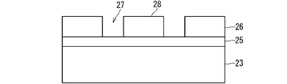
- the protective SiN film 25 is formed (step ST22 in FIG. 6). Then, as shown in FIG. 15, photoengraving is performed on the structure (step ST23 in FIG. 6).
- a SiN film (that is, a protective SiN film 25) is formed on the polished surface 24 of the polycrystalline diamond wafer 23 by a plasma CVD method, for example, with a film thickness of 400 nm.
- a photoresist is formed on the upper surface of the protective SiN film 25, and general photoengraving processes such as pattern exposure and development are carried out. Then, a resist mask 26 is formed on the upper surface of the protective SiN film 25.
- FIG. 16 is a plan view schematically showing an example of a resist mask pattern produced in the present embodiment.
- the resist mass includes a mask portion 28 and an opening 27.
- the resist mask pattern includes a stripe pattern orthogonal to the orientation flat 32 of the polycrystalline diamond wafer 23 and a circumferential pattern along the outer edge 10 of the polycrystalline diamond wafer 23.
- the opening width 29 of the resist mask pattern is set to 10 ⁇ m.
- the mask portion width 30 is 50 ⁇ m, and the outer edge mask portion width 31 is 200 ⁇ m.
- the protective SiN film 25 is etched via the resist mask 26 (step ST24 in FIG. 6).
- the above etching is performed by the RIE method using a mixed gas of CF 4 and O 2 .
- the pattern of the protective SiN film 25 in which the SiN mask opening 33 is formed and the SiN mask portion 34 is formed as shown in FIG. 17 is polycrystalline. It can be obtained on the upper surface of the diamond wafer 23.
- the width of the SiN mask opening 33 and the width of the SiN mask portion 34 was 10 ⁇ m and 50 ⁇ m, which are the same as the width of the resist pattern, respectively.
- the upper surface of the polycrystalline diamond wafer 23 exposed at the bottom surface of the SiN mask opening 33 is also slightly damaged, but this portion is a portion to be etched in a later step. , The damage here is not a problem.
- the RIE method was used for etching the protective SiN film 25, but the method is not limited to this, and for example, a wet etching method may be used.
- the supporting diamond substrate 3 is obtained by etching the upper surface of the polycrystalline diamond wafer 23 with the protective SiN film 25 as a mask (step ST25 in FIG. 6).
- the RIE method using O 2 is applied.
- a processing recess 35 is formed in the lower part of the SiN mask opening 33.
- the processing recess 35 is located inside the outer edge portion 10 of the supporting diamond substrate 3 in a plan view.
- the processing depth 36 of the processing recess 35 is, for example, 10 ⁇ m.
- the gas pressure is relatively high to maintain the etching surface. It is carried out under the condition of suppressing the ion impact component of.
- the polycrystalline diamond wafer 23 located below the protective SiN film 25 undergoes side etching to about 5 ⁇ m in the lateral direction, and the processing width 37 of the processing recess 35 is 90% or more in the longitudinal direction of the recess 35. In the region, it is wider than the width of the SiN mask opening 33, for example, 20 ⁇ m.
- the region that is not etched that is, the terrace portion width 39, which is the width of the surface where the initial diamond-polished surface is maintained (referred to as the terrace portion 38), is, for example, 40 ⁇ m. That is, the distance between the adjacent dents 35 is 0.1 ⁇ m or more and 100 ⁇ m or less in the region of 90% or more in the longitudinal direction of the dents 35. Further, since the thickness of the outer edge portion 10 is 200 ⁇ m as shown in FIGS. 4 and 16, the thickness of the outer edge portion 10 is more than twice the processing width 37 of the processing recess.
- the RIE method using O 2 is applied to the etching of the polycrystalline diamond wafer 23, but the etching method is not limited to this.
- the structure shown in FIG. 18 is immersed in an aqueous hydrofluoric acid solution to remove the protective SiN film 25 (step ST26 in FIG. 6).
- a SiO 2 bonding layer 40 having a film thickness of 1 ⁇ m is formed on the upper surface of the support diamond substrate 3 that has been recessed by a CVD method using TEOS (FIG. 20). Step ST27 in 6. Then, the heat treatment is performed in a nitrogen atmosphere at 700 ° C.
- the roughness Ra was maintained at 0.5 nm.
- the surface roughness of the terrace portion 41 may be deteriorated.
- the upper surface of the terrace portion 41 of the SiO 2 bonding layer 40 can be precisely polished by the CMP method.
- the support diamond substrate 3 in the state where the SiO 2 bonding layer 40 is formed is completed (step ST29 in FIG. 6).
- the SiO 2 bonding layer 40 is formed along the inner wall of the processing recess 35, and is not filled in the space 43 surrounded by the inner wall of the processing recess 35.
- FIGS. 21 and 22 are cross-sectional views showing an example of a state in the middle of the process of manufacturing the composite substrate.
- oxygen plasma is formed by forming the SiO 2 bonding layer 22 formed on the upper surface of the GaN-on diamond substrate 2 and the SiO 2 bonding layer 40 formed on the upper surface of the supporting diamond substrate 3 with oxygen plasma.
- Process in 42 step ST31 in FIG. 7).
- the surface of the SiO 2 bonding layer is activated, and further, it adsorbs moisture in the atmosphere and becomes hydrophilic.
- the oxygen plasma treatment was carried out in the present embodiment, the plasma treatment with an inert gas such as argon or nitrogen may be carried out, or the oxygen plasma treatment may be carried out in order to carry out the hydrophilization treatment more completely. Later, the surface of the SiO 2 bonding layer may be washed with pure water.
- an inert gas such as argon or nitrogen
- step ST31 the surfaces of the SiO 2 bonding layers hydrophilized in step ST31 are brought into contact with each other in the air to be bonded (step ST32 in FIG. 7).
- step ST32 the SiO 2 bonding layer 40 and the SiO 2 bonding layer 22 are bonded in a region other than the processing recess 35.
- the SiO 2 bonding layers When the SiO 2 bonding layers are brought into contact with each other in the atmosphere in this way, the GaN-on-diamond substrate 2 and the supporting diamond substrate 3 are fixed to each other by hydrogen bonds via water molecules adsorbed on the surface.
- the contact area affects the adhesive force, it is necessary to smooth both surfaces to be contacted in order to increase the adhesive force.
- both the GaN-on-diamond substrate 2 and the supporting diamond substrate 3 are transparent to visible light. Therefore, by visual observation, a region that is properly bonded (that is, a bonded region) and a region that is not bonded (a region in which voids are formed between the SiO 2 bonded layers, that is, a non-bonded region). You can see the difference in contrast with.
- the contrast difference due to the presence or absence of the above-mentioned bonding may be difficult to discriminate due to the laminated structure composed of a plurality of transparent films. Further, the above contrast difference may be difficult to discriminate even if a non-junction region is formed by a periodic groove structure. However, in the present embodiment, it was possible to observe a sufficiently discernible contrast difference.
- the bonding region may not expand spontaneously.
- the SiO 2 bonding layers can be forcibly brought into contact with each other and bonded by applying pressure from the outside of the substrate using a roller or the like.
- the atmosphere can escape to the space 43, and there is an advantage that the atmosphere is not isolated in the joint surface.
- both the bonded substrates are heat-treated in a nitrogen atmosphere at 400 ° C. (step ST33 in FIG. 7).
- the composite substrate 1 according to the present embodiment is completed (step ST34 in FIG. 7).
- the composite substrate 1 shown in FIG. 22 is the same as the composite substrate 1 shown in FIGS. 1 and 2.
- the substrate bonding method including the hydrophilic treatment was described in step ST32 in FIG. 7 and step ST33 in FIG. 7, but between the support substrate adhesive layer 16 and the support substrate 17 in FIG.
- a substrate bonding method involving a hydrophilic treatment can also be applied to the bonding method.
- the support substrate adhesive layer 16 and the support substrate 17 are flat substrates in which no dents or the like are formed, there is a risk that poor bonding may occur due to sandwiching the atmosphere when bonding in the atmosphere. Therefore, caution is required.
- both the Si substrate 11 and the support substrate 17 are opaque to visible light, it is necessary to use near-infrared light when evaluating the junction region by visual observation.
- a halogen lamp is used as a light source and the transmitted light is photographed with a CCD camera that excludes an infrared cut filter, the presence or absence of a poorly bonded portion can be confirmed by the contrast difference.
- FIGS. 23, 24, 25, and 26 are cross-sectional views showing an example of a state in the middle of the process of forming the GaN on-diamond transistor.
- the transistor process is applied to the composite substrate 1 (step ST41 in FIG. 8).
- the transistor step includes, for example, an ion injection step for element separation, a metal thin film electrode forming step, a heat treatment step for forming ohmic contacts, and a surface protective SiN film. It includes a film forming step, a photoplate making step for pattern forming, a wet etching step or a dry etching step for pattern forming, and the like.
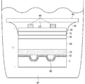
- FIG. 23 schematically shows a state in which electrodes 44 forming a transistor are formed on the AlGaN film 14 and the GaN film 13 which are the upper surfaces of the composite substrate 1.
- the support sapphire glass 45 is adhered to the composite substrate 1 on which the transistor is formed (step ST42 in FIG. 8).
- the purpose of adhering the support sapphire glass 45 to the composite substrate 1 is to hold the substrate when removing the support diamond substrate 3 in the composite substrate 1.
- thermoplastic wax 46 is used to bond a supporting sapphire glass 45 having a diameter larger than that of the composite substrate 1 (for example, a diameter of 3 inches).
- the reason for using sapphire glass is that it will not be damaged by immersion in a hydrofluoric acid aqueous solution in the subsequent process.
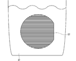
- the composite substrate 1 adhered to the support sapphire glass 45 is immersed in the hydrofluoric acid aqueous solution 47, and the support diamond substrate 3 is removed (step ST43 in FIG. 8).
- both the SiO 2 bonding layer 22 and the SiO 2 bonding layer 40 are soluble in the hydrofluoric acid aqueous solution 47, these bonding layers are dissolved and removed by the step as shown in FIG. 26.
- the composite substrate 1 is separated into a GaN-on-diamond substrate 2 in which the support sapphire glass 45 is attached and a support diamond substrate 3 in which the SiO 2 bonding layer 40 is removed. Will be done.
- the wax 46 is softened by heating the support sapphire glass 45 on a hot plate, and a GaN-on-diamond transistor (that is, an electrode 44 forming the transistor on the upper surface of the GaN-on-diamond substrate 2) is formed from the support sapphire glass 45. The formed structure) is removed.
- a GaN-on-diamond transistor that is, an electrode 44 forming the transistor on the upper surface of the GaN-on-diamond substrate 2 is formed from the support sapphire glass 45. The formed structure) is removed.
- FIG. 27 is a cross-sectional view showing, as a comparative example, an example of a structure having no space formed by a depression, that is, a configuration of a composite substrate in which two substrates are bonded via a thin film bonding layer. ..
- the Si substrate 49 located above and the Si substrate 50 located below are joined with the SiO 2 bonding layer 51 interposed therebetween.
- the film thickness 52 of the SiO 2 bonding layer 51 is 2 ⁇ m.
- FIG. 27 shows a composite substrate of the Si substrate 49 and the Si substrate 50 after being immersed in a hydrofluoric acid aqueous solution having a concentration of 50% by weight for a certain period of time. Therefore, in FIG. 27, the SiO 2 bonding layer 51 is etched by the etching distance 53 from the end portion of the composite substrate.
- the etching distance 53 was 100 ⁇ m per hour of immersion. This is a value that is not inconsistent with the generally known etching rate of SiO 2 (1.5 ⁇ m / min with respect to a hydrofluoric acid aqueous solution having a concentration of 50% by weight). From this value, it can be seen that it takes 280 hours by simple calculation to set the etching distance to 25 mm in order to remove the 2-inch substrate, that is, the substrate having a diameter of 50 mm. This length of time is not industrially valid.
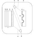
- FIG. 28 is a cross-sectional view showing an example of the configuration of a composite substrate including the support diamond substrate 3 and the GaN on diamond substrate 2 according to the present embodiment.
- FIG. 28 shows a composite substrate after being immersed in a hydrofluoric acid aqueous solution having a concentration of 50% by weight for a certain period of time.
- the progress rate of the etching distance 54 becomes equal to the progress rate of the etching distance 53 of the comparative example shown in FIG. 27.
- the SiO 2 bonding layer 40 and the SiO 2 bonding layer 22 corresponding to the terrace portion width 39 may be etched.
- the terrace portion width 39 is 40 ⁇ m, it is sufficient to etch 20 ⁇ m, which is half the width, and the etching is completed in 13 minutes by simple calculation, and the supporting diamond substrate 3 is used as the GaN-on-diamond substrate 2. Can be removed from.
- the space 43 needs to function as a flow path extending to the end of the supporting diamond substrate 3.
- the width of the terrace portion is 40 ⁇ m and the width of the space 43 is 20 ⁇ m, but the respective dimensions are not limited to this.
- the width of the terrace portion is narrowed, the time required for removing the supporting diamond substrate 3 is shortened, but if the width of the terrace portion is too narrow, the terrace portion falls down and is easily damaged.
- the width of the terrace portion is widened, the bonding force between the GaN-on-diamond substrate 2 and the supporting diamond substrate 3 increases, but even if the width of the terrace portion is wider than 100 ⁇ m, the bonding force is not improved so much. It only increases the time required to remove the supporting diamond substrate 3. In view of the above, it is desirable that the width of the terrace portion is 0.1 ⁇ m or more and 100 ⁇ m or less.
- the hydrofluoric acid aqueous solution which is a chemical solution, needs to infiltrate into the space 43 formed by the processing recess 35, but if the width of the space 43 is narrow, the hydrofluoric acid aqueous solution does not sufficiently infiltrate. In the present embodiment, if the width of the space 43 is narrower than 1 ⁇ m, the hydrofluoric acid aqueous solution does not infiltrate.
- the width of the space 43 is 1 ⁇ m or more and 1 mm or less.
- the support diamond substrate 3 should be easily removed.
- the immersion time required for removing the supporting diamond substrate 3 may be significantly longer than expected.
- a nonionic surfactant is added to the hydrofluoric acid aqueous solution in order to improve the wettability of the wall surface of the processed recess 35 in the above problems.
- the immersion container is installed in a reduced pressure environment. Under the reduced pressure environment, the air filled in the space 43 that functions as a flow path is discharged to the outside of the space 43. Therefore, the hydrofluoric acid aqueous solution is easily filled in the space 43.
- both the addition of the surfactant and the immersion under reduced pressure are carried out, but either one may be carried out or neither of them may be carried out. Further, the type of surfactant to be added is not limited to the above.
- the immersion time required for removing the supporting diamond substrate 3 may be longer than expected. This is especially noticeable when the immersion container is not installed in a reduced pressure environment.
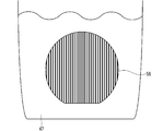
- FIG. 29 is a diagram showing a state in which the composite substrate 56 is immersed in the hydrofluoric acid aqueous solution 47.
- a flow path is shown on the substrate surface to aid understanding, but since the flow path is actually sandwiched between the substrates, it cannot be confirmed from the outside of the composite substrate 56.
- the composite substrate 56 is immersed in a state in which the flow path extends in a direction orthogonal to the liquid surface of the hydrofluoric acid aqueous solution 47.
- FIG. 30 is a diagram showing a state in which the composite substrate 57 is immersed in the hydrofluoric acid aqueous solution 47. Also in FIG. 30, a flow path is shown on the substrate surface to aid understanding, but since the flow path is actually sandwiched between the substrates, it cannot be confirmed from the outside of the composite substrate 57.
- the composite substrate 57 is immersed in a state in which the flow path extends parallel to the liquid surface of the hydrofluoric acid aqueous solution 47.
- the reason why the time required for removing the supporting diamond substrate 3 differs depending on the installation direction of the composite substrate is that the chemical solution invades the flow path due to the density difference between the chemical solution and air.
- the flow path extends in a direction orthogonal to the liquid surface of the hydrofluoric acid aqueous solution 47. It is important to immerse the composite substrate.
- the flow paths are immersed in a state in which the flow paths extend in which direction.
- the time required for removing the supporting diamond substrate 3 can be shortened.
- FIG. 33 is a diagram showing other examples of the semiconductor substrate and the support substrate constituting the composite substrate according to the present embodiment.
- a machining recess 35A and a machining recess 35B extending in a direction intersecting the machining recess 35A are formed on the joint surface of the support diamond substrate 3A between the support diamond substrate 3A and the GaN on diamond substrate 2.
- the angle formed by the extending direction of the processing recess 35A and the extending direction of the processing recess 35B is, for example, 10 ° or more and 90 ° or less.
- a radial flow path may be formed, or a joint portion is joined by a plurality of point-shaped terrace portions, and the rest is a joint portion that functions as a flow path. You may.
- a terrace portion is formed over the entire circumference of the outer edge portion 10 of the supporting diamond substrate 3.
- the space 43 is closed by the terrace portion over the entire circumference of the outer edge portion 10.
- step ST43 of FIG. 8 the support diamond substrate 3 is removed using the hydrofluoric acid aqueous solution 47, but prior to that step, the transistor step of step ST41 in FIG. An aqueous acid solution is used.
- the support diamond substrate 3 may be unintentionally removed in step ST41 in FIG. 8, and the support diamond substrate 3 may not be able to serve as the support substrate. There is.
- a terrace portion is formed over the entire circumference of the outer edge portion 10 in order to adjust the timing of starting removal. Then, the terrace portion delays the timing at which the hydrofluoric acid aqueous solution infiltrates into the space 43.
- the radial width of the terrace portion formed on the outer edge portion 10 of the substrate is set to 200 ⁇ m. Then, the infiltration of the hydrofluoric acid aqueous solution into the space 43 can be delayed by about 120 minutes.
- the radial width of the terrace portion is set to 200 ⁇ m, but the radial width of the terrace portion is not limited to this value and may be changed as necessary.
- the terrace portion is formed along the (outermost) outer edge portion 10 of the substrate, but it may be formed at a position moved inward by a certain width from the outermost edge portion of the substrate.
- a terrace portion over the entire circumference may be formed, for example, about 1 mm inside from the end portion of the substrate.
- the composite substrate according to the present embodiment has the same shape as the composite substrate shown in the first embodiment, that is, the composite substrate shown in FIGS. 1, 2 and 22, but the inside of the flow path is inside. It is a vacuum.
- a step of preparing a GaN-on-diamond substrate there are four steps in total, that is, a step of preparing a GaN-on-diamond substrate, a step of preparing a supporting diamond substrate, a step of manufacturing a composite substrate, and a step of forming a GaN-on-diamond transistor.
- steps in total that is, a step of preparing a GaN-on-diamond substrate, a step of preparing a supporting diamond substrate, a step of manufacturing a composite substrate, and a step of forming a GaN-on-diamond transistor.
- FIG. 31 is a flowchart showing a process of manufacturing a composite substrate.
- FIG. 32 is a cross-sectional view showing an example of a state in the middle of the process of manufacturing the composite substrate.
- the GaN-on-diamond substrate 2 and the supporting diamond substrate 3 are arranged in the bonding apparatus chamber 58 maintained in a high vacuum so that the bonding surfaces face each other while being separated from each other (step ST51 in FIG. 31).
- the bonding surfaces of both substrates that is, the SiO 2 bonding layer 22 and the SiO 2 bonding layer 40, are activated by the ion beam 60 emitted from the ion gun 59, respectively (step ST52 in FIG. 31).
- an argon ion beam is used for the surface activation treatment.
- the purpose of the argon ion beam treatment here is to remove deposits or contaminants on the surface of the joint surface, and to generate unbonded hands (dangling bonds) on the surface of the joint surface.
- both substrates are brought into contact with each other and further pressurized while the inside of the joining device chamber 58 is kept in a high vacuum. By doing so, both substrates are joined (step ST53 in FIG. 31).
- the above surface activation treatment and joining treatment are continuously performed under high vacuum. Therefore, the unbonded hands formed on the surface of the joint surface are not terminated and are combined with the unbonded hands on the joint surface on the contacting side. Therefore, a strong bond is formed between the two substrates.
- the inside of the space 43 formed after the joining surfaces are joined together has a high vacuum as high as the inside of the joining device chamber 58. Therefore, when the supporting diamond substrate 3 is removed, the chemical solution can be quickly infiltrated into the space 43. That is, the decompression in the space 43 can be realized without placing the dipping chemical solution itself in the depressurized environment. As a result, the support diamond substrate 3 can be removed in a short time.
- the space 43 has a high vacuum, but it does not necessarily have to be a high vacuum, it may be a negative pressure rather than the atmospheric pressure, and the space 43 is, for example, about 0.05 MPa. Even if it is done, a sufficient effect can be obtained.
- the bonding in vacuum is performed in the void (unbonded portion) or the space 43 of the bonding interface even in the high temperature process or the vacuum process in the transistor process which is a subsequent process. It is possible to suppress the risk of joint peeling due to the expansion of the enclosed gas.
- the composite substrate can be manufactured while shortening the time required for removing the support diamond substrate 3 (step ST54 in FIG. 31).
- the replacement may be made across a plurality of embodiments. That is, it may be the case that the respective configurations shown in the examples in different embodiments are combined to produce the same effect.
- a first bonding material is formed on the first surface of the first substrate.
- the first substrate corresponds to, for example, the support diamond substrate 3.
- the first bonding material corresponds to, for example, the SiO 2 bonding layer 40.
- at least one recess located inside the outer edge portion 10 in the plan view of the supporting diamond substrate 3 is formed on the first surface.
- the dent corresponds to, for example, the processed dent 35.
- the SiO 2 bonding layer 40 is formed along the inner wall of the processing recess 35. Further, the SiO 2 bonding layer 40 is not filled in the space 43 surrounded by the inner wall of the processing recess 35.
- a second bonding material is formed on the second surface of the second substrate.
- the second substrate corresponds to, for example, the GaN-on-diamond substrate 2.
- the second bonding material corresponds to, for example, the SiO 2 bonding layer 22. Then, the SiO 2 bonding layer 40 and the SiO 2 bonding layer 22 are bonded in a region other than the processing recess 35.
- the dissolution liquid penetrates into the space 43 surrounded by the inner wall of the processing recess 35, so that the SiO 2 bonding layer 40 and the SiO 2 bonding layer 22 are dissolved earlier, so that the supporting diamond substrate 3 is removed.
- the time required for this can be shortened.
- the processing recess 35 is formed inside the outer edge portion 10, the SiO 2 bonding layer 40 and the SiO 2 bonding layer 22 are melted in an unintended process, and the composite substrate is prevented from peeling off. Can be done.
- the junction between the SiO 2 bonding layer 40 and the SiO 2 bonding layer 22 is activated with oxygen plasma and a SiO 2 bonding layer 40 and the SiO 2 bonding layer 22 It is done after letting it.
- the composite substrate 1 can be formed by joining the activated SiO 2 bonding layer 40 and the activated SiO 2 bonding layer 22.
- the junction between the SiO 2 bonding layer 40 and the SiO 2 bonding layer 22, an ion beam and a SiO 2 bonding layer 40 and the SiO 2 bonding layer 22 under vacuum environment It is done after activation with.
- the inside of the space 43 formed in the composite substrate 1 after joining is in a vacuum state, so that the dissolved liquid easily penetrates into the space 43.
- the composite substrate 1 in which the SiO 2 bonding layer 40 and the SiO 2 bonding layer 22 are bonded is immersed in the solution.
- the supporting diamond substrate 3 can be removed from the GaN-on-diamond substrate 2 by dissolving the SiO 2 bonding layer 22 and the SiO 2 bonding layer 40 with the dissolution liquid.
- the solution is a hydrofluoric acid aqueous solution 47.
- the supporting diamond substrate 3 can be removed from the GaN-on-diamond substrate 2 by dissolving the SiO 2 bonding layer 22 and the SiO 2 bonding layer 40 with the hydrofluoric acid aqueous solution 47.
- the composite substrate 1 is immersed in the solution in a reduced pressure environment. According to such a configuration, the air filled in the space 43 that functions as a flow path is easily discharged to the outside of the space 43, so that the hydrofluoric acid aqueous solution 47 is easily filled in the space 43.
- the processing recess 35 is formed so as to extend in the first direction on the first surface. Then, the composite substrate 1 is immersed in the dissolution liquid by arranging the composite substrate 1 so that the first direction intersects the liquid surface of the dissolution liquid. According to such a configuration, it is necessary to remove the support diamond substrate 3 because the time required for the solution infiltrated from the outer edge portion 10 of the support diamond substrate 3 to reach the central portion of the support diamond substrate 3 is shortened. The time can be shortened.
- the composite substrate includes a supporting diamond substrate 3 having a first surface, a GaN-on-diamond substrate 2 having a second surface, and a SiO formed on the first surface. It includes a two- bonding layer 40 and a SiO 2 bonding layer 22 formed on a second surface and bonded to the SiO 2 bonding layer 40. Then, at least one processing recess 35 located inside the outer edge portion 10 in the plan view of the support diamond substrate 3 is formed on the first surface. Further, the SiO 2 bonding layer 40 is formed along the inner wall of the processed recess 35, and is not filled in the space 43 surrounded by the inner wall of the processed recess 35. Further, the SiO 2 bonding layer 40 and the SiO 2 bonding layer 22 are bonded in a region other than the processing recess 35.
- the dissolution liquid penetrates into the space 43 surrounded by the inner wall of the processing recess 35, so that the SiO 2 bonding layer 40 and the SiO 2 bonding layer 22 are dissolved earlier, so that the supporting diamond substrate 3 is removed.
- the time required for this can be shortened.
- the processing recess 35 is formed inside the outer edge portion 10, the SiO 2 bonding layer 40 and the SiO 2 bonding layer 22 are melted in an unintended process, and the composite substrate is prevented from peeling off. Can be done.
- the space 43 is a space extending in at least two directions along the first surface.
- the angle formed between the two directions in which the space 43 extends is 10 ° or more and 90 ° or less. According to such a configuration, the hydrofluoric acid aqueous solution 47 easily penetrates into the space 43 regardless of the orientation when the composite substrate is immersed in the hydrofluoric acid aqueous solution 47, so that the time required for removing the supporting diamond substrate 3 is required. It won't be long.
- the width of the outer edge portion 10 is at least twice the interval between the processing recesses 35. According to such a configuration, it is possible to effectively prevent the support diamond substrate 3 from being inadvertently peeled off even in a step of using a chemical solution other than the step of removing the support diamond substrate 3.
- the width of the processing recess 35 is 1 ⁇ m or more and 1 mm or less. According to such a configuration, the solution can be effectively infiltrated into the space 43 in the processing recess 35, so that the time required for removing the supporting diamond substrate 3 can be shortened.
- a plurality of processing dents 35 are provided.
- the distance between the adjacent processing dents 35 is 0.1 ⁇ m or more and 100 ⁇ m or less.
- the gap portion that is, the portion of the GaN-on-diamond substrate 2 having no support is bent and the parallelism with the supporting diamond substrate 3 changes. It can be suppressed that it ends up. Therefore, the parallelism between the bonded support diamond substrate 3 and the GaN-on-diamond substrate 2 can be maintained.
- the support diamond substrate 3 is a diamond substrate. According to such a configuration, by supporting by the supporting diamond substrate 3, it is possible to apply the transistor process to the GaN on diamond substrate 2 without bending the GaN on diamond substrate 2.
- each component in the above-described embodiment is a conceptual unit, and within the scope of the technique disclosed in the present specification, one component is composed of a plurality of structures. And the case where one component corresponds to a part of a structure, and further, the case where a plurality of components are provided in one structure.
- each component in the above-described embodiment shall include a structure having another structure or shape as long as it exhibits the same function.
- the material when a material name or the like is described without being specified, the material contains other additives, for example, an alloy, etc., unless a contradiction occurs. It shall be included.
Landscapes
- Engineering & Computer Science (AREA)
- Mechanical Engineering (AREA)
- Physics & Mathematics (AREA)
- Plasma & Fusion (AREA)
- Recrystallisation Techniques (AREA)
- Junction Field-Effect Transistors (AREA)
Abstract
Description
以下、本実施の形態に関する複合基板の製造方法、および、複合基板について説明する。
以下に、本実施の形態に関する複合基板について、図面を参照し説明する。
次に、本実施の形態に関する複合基板の製造方法について説明する。
はじめに、GaNオンダイヤモンド基板を準備する工程について、図5、図9、図10、図11、図12および図13を参照しつつ説明する。
次に、支持ダイヤモンド基板を準備する工程について、図6、図14、図15、図16、図17、図18、図19および図20を参照しつつ説明する。
次に、複合基板を作製する工程について、図7、図21および図22を参照しつつ説明する。
次に、GaNオンダイヤモンドトランジスタを形成する工程について、図8、図23、図24、図25および図26を参照しつつ説明する。
次に、本実施の形態に関する複合基板1における、加工くぼみ35によって形成される空間43の意義について説明する。
本実施の形態では、図16に例が示されたレジストマスクパターンを用いて加工くぼみ35を形成するため、支持ダイヤモンド基板3の外縁部10の全周に渡ってテラス部が形成される。そして、外縁部10の全周に渡るテラス部によって、空間43が閉塞されている。以下では、全周に渡るテラス部の意義について説明する。
本実施の形態に関する複合基板の製造方法、および、複合基板について説明する。なお、以下の説明においては、以上に記載された実施の形態で説明された構成要素と同様の構成要素については同じ符号を付して図示し、その詳細な説明については適宜省略するものとする。
本実施の形態に関する複合基板は、第1の実施の形態に示された複合基板、すなわち、図1、図2および図22に示された複合基板と同一の形状であるが、流路内が真空である。
次に、本実施の形態に関する複合基板の製造方法について説明する。
複合基板を作製する工程について、図31および図32を参照しつつ説明する。
次に、以上に記載された実施の形態によって生じる効果の例を示す。なお、以下の説明においては、以上に記載された実施の形態に例が示された具体的な構成に基づいて当該効果が記載されるが、同様の効果が生じる範囲で、本願明細書に例が示される他の具体的な構成と置き換えられてもよい。
以上に記載された実施の形態では、それぞれの構成要素の材質、材料、寸法、形状、相対的配置関係または実施の条件などについても記載する場合があるが、これらはすべての局面においてひとつの例であって、本願明細書に記載されたものに限られることはないものとする。
Claims (13)
- 第1の基板(3)の第1の表面に、第1の接合材(40)を形成し、
前記第1の表面には、前記第1の基板(3)の平面視における外縁部(10)よりも内側に位置する少なくとも1つのくぼみ(35)が形成され、
前記第1の接合材(40)は、前記くぼみ(35)の内壁に沿って形成され、かつ、前記くぼみ(35)の前記内壁に囲まれる空間(43)には充填されず、
第2の基板(2)の第2の表面に、第2の接合材(22)を形成し、
前記第1の接合材(40)と前記第2の接合材(22)とを、前記くぼみ(35)を除く領域において接合する、
複合基板の製造方法。 - 請求項1に記載の複合基板の製造方法であり、
前記第1の接合材(40)と前記第2の接合材(22)との接合は、前記第1の接合材(40)と前記第2の接合材(22)とを酸素プラズマを用いて活性化させた後で行われる、
複合基板の製造方法。 - 請求項1に記載の複合基板の製造方法であり、
前記第1の接合材(40)と前記第2の接合材(22)との接合は、真空環境下において前記第1の接合材(40)と前記第2の接合材(22)とをイオンビームを用いて活性化させた後で行われる、
複合基板の製造方法。 - 請求項1から3のうちのいずれか1つに記載の複合基板の製造方法であり、
前記第1の接合材(40)と前記第2の接合材(22)とが接合された状態の複合基板(1)を、溶解液(47)に浸漬させる、
複合基板の製造方法。 - 請求項4に記載の複合基板の製造方法であり、
前記溶解液は、フッ酸水溶液である、
複合基板の製造方法。 - 請求項4または5に記載の複合基板の製造方法であり、
前記複合基板(1)の前記溶解液(47)への浸漬は、減圧環境下において行われる、
複合基板の製造方法。 - 請求項4から6のうちのいずれか1つに記載の複合基板の製造方法であり、
前記くぼみ(35)が、前記第1の表面における第1の方向に延びて形成され、
前記複合基板(1)の前記溶解液(47)への浸漬は、前記第1の方向が前記溶解液(47)の液面と交差するように前記複合基板(1)を配置して行われる、
複合基板の製造方法。 - 第1の表面を有する第1の基板(3)と、
第2の表面を有する第2の基板(2)と、
前記第1の表面に形成される第1の接合材(40)と、
前記第2の表面に形成され、かつ、前記第1の接合材(40)と接合される第2の接合材(22)とを備え、
前記第1の表面には、前記第1の基板(3)の平面視における外縁部(10)よりも内側に位置する少なくとも1つのくぼみ(35)が形成され、
前記第1の接合材(40)は、前記くぼみ(35)の内壁に沿って形成され、かつ、前記くぼみ(35)の前記内壁に囲まれる空間(43)には充填されず、
前記第1の接合材(40)と前記第2の接合材(22)とは、前記くぼみ(35)を除く領域において接合される、
複合基板(1)。 - 請求項8に記載の複合基板(1)であり、
前記空間(43)は、前記第1の表面に沿って少なくとも2方向に延びる空間であり、
前記空間(43)が延びる2方向の間のなす角が、10°以上、かつ、90°以下である、
複合基板(1)。 - 請求項8または9に記載の複合基板(1)であり、
前記外縁部(10)の幅は、前記くぼみ(35)間の間隔の2倍以上である、
複合基板(1)。 - 請求項8から10のうちのいずれか1つに記載の複合基板(1)であり、
前記くぼみ(35)の幅は、1μm以上、かつ、1mm以下である、
複合基板(1)。 - 請求項8から11のうちのいずれか1つに記載の複合基板(1)であり、
前記くぼみ(35)は複数備えられ、
隣接する前記くぼみ(35)間の間隔は、0.1μm以上、かつ、100μm以下である、
複合基板(1)。 - 請求項8から12のうちのいずれか1つに記載の複合基板(1)であり、
前記第1の基板(3)は、ダイヤモンド基板である、
複合基板(1)。
Priority Applications (6)
| Application Number | Priority Date | Filing Date | Title |
|---|---|---|---|
| PCT/JP2019/024725 WO2020255376A1 (ja) | 2019-06-21 | 2019-06-21 | 複合基板の製造方法、および、複合基板 |
| CN201980097561.9A CN114365262B (zh) | 2019-06-21 | 2019-06-21 | 复合基板的制造方法及复合基板 |
| US17/608,570 US12269107B2 (en) | 2019-06-21 | 2019-06-21 | Method for manufacturing composite substrate, and composite substrate |
| KR1020217040425A KR102550295B1 (ko) | 2019-06-21 | 2019-06-21 | 복합 기판의 제조 방법 및 복합 기판 |
| JP2019561205A JP6727460B1 (ja) | 2019-06-21 | 2019-06-21 | 複合基板の製造方法、および、複合基板 |
| EP19933414.5A EP3989263A4 (en) | 2019-06-21 | 2019-06-21 | Method for manufacturing composite substrate, and composite substrate |
Applications Claiming Priority (1)
| Application Number | Priority Date | Filing Date | Title |
|---|---|---|---|
| PCT/JP2019/024725 WO2020255376A1 (ja) | 2019-06-21 | 2019-06-21 | 複合基板の製造方法、および、複合基板 |
Publications (1)
| Publication Number | Publication Date |
|---|---|
| WO2020255376A1 true WO2020255376A1 (ja) | 2020-12-24 |
Family
ID=71663966
Family Applications (1)
| Application Number | Title | Priority Date | Filing Date |
|---|---|---|---|
| PCT/JP2019/024725 Ceased WO2020255376A1 (ja) | 2019-06-21 | 2019-06-21 | 複合基板の製造方法、および、複合基板 |
Country Status (6)
| Country | Link |
|---|---|
| US (1) | US12269107B2 (ja) |
| EP (1) | EP3989263A4 (ja) |
| JP (1) | JP6727460B1 (ja) |
| KR (1) | KR102550295B1 (ja) |
| CN (1) | CN114365262B (ja) |
| WO (1) | WO2020255376A1 (ja) |
Cited By (5)
| Publication number | Priority date | Publication date | Assignee | Title |
|---|---|---|---|---|
| CN115172311A (zh) * | 2021-04-02 | 2022-10-11 | 世界先进积体电路股份有限公司 | 半导体结构及其制作方法 |
| WO2024004314A1 (ja) * | 2022-06-30 | 2024-01-04 | 日本碍子株式会社 | 複合基板および13族元素窒化物エピタキシャル成長用基板 |
| JP2024029834A (ja) * | 2022-08-23 | 2024-03-07 | 株式会社ディスコ | ウェーハの加工方法 |
| JP2024130242A (ja) * | 2023-03-14 | 2024-09-30 | 三菱電機株式会社 | 半導体装置の製造方法、半導体製造装置及び半導体装置 |
| WO2025094432A1 (ja) * | 2022-11-02 | 2025-05-08 | ランテクニカルサービス株式会社 | 剥離方法 |
Families Citing this family (3)
| Publication number | Priority date | Publication date | Assignee | Title |
|---|---|---|---|---|
| KR102550295B1 (ko) * | 2019-06-21 | 2023-06-30 | 미쓰비시덴키 가부시키가이샤 | 복합 기판의 제조 방법 및 복합 기판 |
| US12027413B2 (en) * | 2021-08-22 | 2024-07-02 | Vanguard International Semiconductor Corporation | Semiconductor structure and method of fabricating the same |
| CN115424928B (zh) * | 2022-09-20 | 2023-12-29 | 上海新微半导体有限公司 | 金刚石基外延结构及其制备方法、半导体器件的制备方法 |
Citations (6)
| Publication number | Priority date | Publication date | Assignee | Title |
|---|---|---|---|---|
| JPH0661340A (ja) * | 1992-08-05 | 1994-03-04 | Fujitsu Ltd | 張り合わせ半導体基板の製造方法 |
| JP2003257805A (ja) * | 2002-02-28 | 2003-09-12 | Toshiba Corp | 半導体ウエハ及びその製造方法 |
| JP2008181990A (ja) * | 2007-01-24 | 2008-08-07 | Sony Corp | 半導体装置の製造方法および半導体装置 |
| JP2015522213A (ja) | 2012-07-03 | 2015-08-03 | エレメント シックス テクノロジーズ ユーエス コーポレイション | 半導体−オン−ダイヤモンドウェハのハンドルおよび製造方法 |
| JP2016509372A (ja) * | 2013-01-22 | 2016-03-24 | コミッサリア ア レネルジー アトミーク エ オ ゼネルジ ザルタナテイヴ | 直接接合による構造体の製造方法 |
| JP2016171307A (ja) * | 2015-03-10 | 2016-09-23 | 株式会社デンソー | 基板接合方法 |
Family Cites Families (11)
| Publication number | Priority date | Publication date | Assignee | Title |
|---|---|---|---|---|
| JPH02202023A (ja) | 1989-01-31 | 1990-08-10 | Fujitsu Ltd | 半導体装置の製造方法 |
| US6425972B1 (en) * | 1997-06-18 | 2002-07-30 | Calipher Technologies Corp. | Methods of manufacturing microfabricated substrates |
| US6984571B1 (en) | 1999-10-01 | 2006-01-10 | Ziptronix, Inc. | Three dimensional device integration method and integrated device |
| JP2006032423A (ja) * | 2004-07-12 | 2006-02-02 | Toshiba Corp | インプリント加工用スタンパーおよびその製造方法 |
| US8101498B2 (en) * | 2005-04-21 | 2012-01-24 | Pinnington Thomas Henry | Bonded intermediate substrate and method of making same |
| JP5114017B2 (ja) * | 2006-05-11 | 2013-01-09 | オリンパス株式会社 | 半導体装置、該半導体装置の製造方法 |
| TW201237963A (en) * | 2011-03-08 | 2012-09-16 | Univ Nat Chiao Tung | Method of semiconductor manufacturing process |
| WO2014020906A1 (ja) | 2012-07-30 | 2014-02-06 | 住友化学株式会社 | 複合基板の製造方法および半導体結晶層形成基板の製造方法 |
| JP2014175335A (ja) | 2013-03-06 | 2014-09-22 | Sumitomo Electric Ind Ltd | 複合積層基板およびiii族窒化物半導体デバイスの製造方法 |
| CN106783998A (zh) * | 2016-12-16 | 2017-05-31 | 中国电子科技集团公司第五十五研究所 | 一种基于金刚石衬底的氮化镓高电子迁移率晶体管及其制备方法 |
| KR102550295B1 (ko) * | 2019-06-21 | 2023-06-30 | 미쓰비시덴키 가부시키가이샤 | 복합 기판의 제조 방법 및 복합 기판 |
-
2019
- 2019-06-21 KR KR1020217040425A patent/KR102550295B1/ko active Active
- 2019-06-21 CN CN201980097561.9A patent/CN114365262B/zh active Active
- 2019-06-21 JP JP2019561205A patent/JP6727460B1/ja active Active
- 2019-06-21 EP EP19933414.5A patent/EP3989263A4/en active Pending
- 2019-06-21 US US17/608,570 patent/US12269107B2/en active Active
- 2019-06-21 WO PCT/JP2019/024725 patent/WO2020255376A1/ja not_active Ceased
Patent Citations (6)
| Publication number | Priority date | Publication date | Assignee | Title |
|---|---|---|---|---|
| JPH0661340A (ja) * | 1992-08-05 | 1994-03-04 | Fujitsu Ltd | 張り合わせ半導体基板の製造方法 |
| JP2003257805A (ja) * | 2002-02-28 | 2003-09-12 | Toshiba Corp | 半導体ウエハ及びその製造方法 |
| JP2008181990A (ja) * | 2007-01-24 | 2008-08-07 | Sony Corp | 半導体装置の製造方法および半導体装置 |
| JP2015522213A (ja) | 2012-07-03 | 2015-08-03 | エレメント シックス テクノロジーズ ユーエス コーポレイション | 半導体−オン−ダイヤモンドウェハのハンドルおよび製造方法 |
| JP2016509372A (ja) * | 2013-01-22 | 2016-03-24 | コミッサリア ア レネルジー アトミーク エ オ ゼネルジ ザルタナテイヴ | 直接接合による構造体の製造方法 |
| JP2016171307A (ja) * | 2015-03-10 | 2016-09-23 | 株式会社デンソー | 基板接合方法 |
Non-Patent Citations (1)
| Title |
|---|
| See also references of EP3989263A4 |
Cited By (10)
| Publication number | Priority date | Publication date | Assignee | Title |
|---|---|---|---|---|
| CN115172311A (zh) * | 2021-04-02 | 2022-10-11 | 世界先进积体电路股份有限公司 | 半导体结构及其制作方法 |
| CN115172311B (zh) * | 2021-04-02 | 2025-09-16 | 世界先进积体电路股份有限公司 | 半导体结构及其制作方法 |
| WO2024004314A1 (ja) * | 2022-06-30 | 2024-01-04 | 日本碍子株式会社 | 複合基板および13族元素窒化物エピタキシャル成長用基板 |
| JPWO2024004314A1 (ja) * | 2022-06-30 | 2024-01-04 | ||
| JP7710614B2 (ja) | 2022-06-30 | 2025-07-18 | 日本碍子株式会社 | 複合基板および13族元素窒化物エピタキシャル成長用基板 |
| JP2024029834A (ja) * | 2022-08-23 | 2024-03-07 | 株式会社ディスコ | ウェーハの加工方法 |
| JP7862262B2 (ja) | 2022-08-23 | 2026-05-19 | 株式会社ディスコ | ウェーハの加工方法 |
| WO2025094432A1 (ja) * | 2022-11-02 | 2025-05-08 | ランテクニカルサービス株式会社 | 剥離方法 |
| JP2024130242A (ja) * | 2023-03-14 | 2024-09-30 | 三菱電機株式会社 | 半導体装置の製造方法、半導体製造装置及び半導体装置 |
| JP7823615B2 (ja) | 2023-03-14 | 2026-03-04 | 三菱電機株式会社 | 半導体装置の製造方法、半導体製造装置及び半導体装置 |
Also Published As
| Publication number | Publication date |
|---|---|
| EP3989263A1 (en) | 2022-04-27 |
| JPWO2020255376A1 (ja) | 2021-09-13 |
| US20220314357A1 (en) | 2022-10-06 |
| CN114365262A (zh) | 2022-04-15 |
| US12269107B2 (en) | 2025-04-08 |
| KR20220006614A (ko) | 2022-01-17 |
| JP6727460B1 (ja) | 2020-07-22 |
| KR102550295B1 (ko) | 2023-06-30 |
| CN114365262B (zh) | 2025-12-12 |
| EP3989263A4 (en) | 2022-06-29 |
Similar Documents
| Publication | Publication Date | Title |
|---|---|---|
| JP6727460B1 (ja) | 複合基板の製造方法、および、複合基板 | |
| TW404061B (en) | Semiconductor substrate and method of manufacturing the same | |
| JP4745249B2 (ja) | 決定可能な熱膨張係数を有する基板 | |
| JP5065748B2 (ja) | 貼り合わせウエーハの製造方法 | |
| JP2016119489A (ja) | 複合基板の製造方法 | |
| JP6866150B2 (ja) | 2つの構造体間の直接接合を実行する方法 | |
| TWI242796B (en) | Substrate and manufacturing method therefor | |
| JP7594585B2 (ja) | SiCでできたキャリア基材上に単結晶SiCの薄層を備える複合構造を作成するプロセス | |
| JP7620646B2 (ja) | 非常に高い温度に対応する剥離可能な仮基板、及び前記基板から加工層を移動させるプロセス | |
| WO2010143475A1 (ja) | 圧電デバイスの製造方法 | |
| JP2008021992A (ja) | 接合界面安定化のための熱処理 | |
| JP2011061084A (ja) | 貼り合わせ基板の製造方法 | |
| FR2839199A1 (fr) | Procede de fabrication de substrats avec detachement d'un support temporaire, et substrat associe | |
| CN113889411B (zh) | 一种带金刚石微柱阵列的金刚石基GaN材料制备方法 | |
| JPH0963912A (ja) | 貼り合わせ基板製造方法 | |
| JP2007227415A (ja) | 貼り合わせ基板の製造方法および貼り合わせ基板 | |
| JP7186872B2 (ja) | 半導体基板の製造方法および半導体装置の製造方法 | |
| US7605055B2 (en) | Wafer with diamond layer | |
| JP2010502555A (ja) | GaN基板の製造方法 | |
| WO2024190086A1 (ja) | 半導体基板の製造方法、半導体基板、及び半導体装置 | |
| US20050130393A1 (en) | Method for improving the quality of heterostructure | |
| JP3754818B2 (ja) | 半導体基板の作製方法 | |
| TWI904594B (zh) | 碳化矽晶圓的製造方法 | |
| TWI861253B (zh) | 用於製作複合結構之方法,該複合結構包含一單晶SiC薄層在一SiC載體底材上 | |
| JP4690734B2 (ja) | 単結晶SiC基板の製造方法 |
Legal Events
| Date | Code | Title | Description |
|---|---|---|---|
| ENP | Entry into the national phase |
Ref document number: 2019561205 Country of ref document: JP Kind code of ref document: A |
|
| 121 | Ep: the epo has been informed by wipo that ep was designated in this application |
Ref document number: 19933414 Country of ref document: EP Kind code of ref document: A1 |
|
| ENP | Entry into the national phase |
Ref document number: 20217040425 Country of ref document: KR Kind code of ref document: A |
|
| NENP | Non-entry into the national phase |
Ref country code: DE |
|
| WWE | Wipo information: entry into national phase |
Ref document number: 2019933414 Country of ref document: EP |
|
| WWG | Wipo information: grant in national office |
Ref document number: 17608570 Country of ref document: US |