WO2020255878A1 - Structure de connexion de substrat flexible et barre omnibus, module de câblage et module de stockage de l'électricité - Google Patents
Structure de connexion de substrat flexible et barre omnibus, module de câblage et module de stockage de l'électricité Download PDFInfo
- Publication number
- WO2020255878A1 WO2020255878A1 PCT/JP2020/023220 JP2020023220W WO2020255878A1 WO 2020255878 A1 WO2020255878 A1 WO 2020255878A1 JP 2020023220 W JP2020023220 W JP 2020023220W WO 2020255878 A1 WO2020255878 A1 WO 2020255878A1
- Authority
- WO
- WIPO (PCT)
- Prior art keywords
- bus bar
- land
- connection
- base material
- metal
- Prior art date
- Legal status (The legal status is an assumption and is not a legal conclusion. Google has not performed a legal analysis and makes no representation as to the accuracy of the status listed.)
- Ceased
Links
Images




Classifications
-
- H—ELECTRICITY
- H01—ELECTRIC ELEMENTS
- H01M—PROCESSES OR MEANS, e.g. BATTERIES, FOR THE DIRECT CONVERSION OF CHEMICAL ENERGY INTO ELECTRICAL ENERGY
- H01M50/00—Constructional details or processes of manufacture of the non-active parts of electrochemical cells other than fuel cells, e.g. hybrid cells
- H01M50/50—Current conducting connections for cells or batteries
- H01M50/502—Interconnectors for connecting terminals of adjacent batteries; Interconnectors for connecting cells outside a battery casing
- H01M50/505—Interconnectors for connecting terminals of adjacent batteries; Interconnectors for connecting cells outside a battery casing comprising a single busbar
-
- H—ELECTRICITY
- H01—ELECTRIC ELEMENTS
- H01M—PROCESSES OR MEANS, e.g. BATTERIES, FOR THE DIRECT CONVERSION OF CHEMICAL ENERGY INTO ELECTRICAL ENERGY
- H01M50/00—Constructional details or processes of manufacture of the non-active parts of electrochemical cells other than fuel cells, e.g. hybrid cells
- H01M50/50—Current conducting connections for cells or batteries
- H01M50/502—Interconnectors for connecting terminals of adjacent batteries; Interconnectors for connecting cells outside a battery casing
- H01M50/519—Interconnectors for connecting terminals of adjacent batteries; Interconnectors for connecting cells outside a battery casing comprising printed circuit boards [PCB]
-
- H—ELECTRICITY
- H01—ELECTRIC ELEMENTS
- H01M—PROCESSES OR MEANS, e.g. BATTERIES, FOR THE DIRECT CONVERSION OF CHEMICAL ENERGY INTO ELECTRICAL ENERGY
- H01M50/00—Constructional details or processes of manufacture of the non-active parts of electrochemical cells other than fuel cells, e.g. hybrid cells
- H01M50/20—Mountings; Secondary casings or frames; Racks, modules or packs; Suspension devices; Shock absorbers; Transport or carrying devices; Holders
- H01M50/204—Racks, modules or packs for multiple batteries or multiple cells
- H01M50/207—Racks, modules or packs for multiple batteries or multiple cells characterised by their shape
- H01M50/209—Racks, modules or packs for multiple batteries or multiple cells characterised by their shape adapted for prismatic or rectangular cells
-
- H—ELECTRICITY
- H01—ELECTRIC ELEMENTS
- H01M—PROCESSES OR MEANS, e.g. BATTERIES, FOR THE DIRECT CONVERSION OF CHEMICAL ENERGY INTO ELECTRICAL ENERGY
- H01M50/00—Constructional details or processes of manufacture of the non-active parts of electrochemical cells other than fuel cells, e.g. hybrid cells
- H01M50/20—Mountings; Secondary casings or frames; Racks, modules or packs; Suspension devices; Shock absorbers; Transport or carrying devices; Holders
- H01M50/284—Mountings; Secondary casings or frames; Racks, modules or packs; Suspension devices; Shock absorbers; Transport or carrying devices; Holders with incorporated circuit boards, e.g. printed circuit boards [PCB]
-
- H—ELECTRICITY
- H01—ELECTRIC ELEMENTS
- H01M—PROCESSES OR MEANS, e.g. BATTERIES, FOR THE DIRECT CONVERSION OF CHEMICAL ENERGY INTO ELECTRICAL ENERGY
- H01M50/00—Constructional details or processes of manufacture of the non-active parts of electrochemical cells other than fuel cells, e.g. hybrid cells
- H01M50/50—Current conducting connections for cells or batteries
- H01M50/502—Interconnectors for connecting terminals of adjacent batteries; Interconnectors for connecting cells outside a battery casing
- H01M50/503—Interconnectors for connecting terminals of adjacent batteries; Interconnectors for connecting cells outside a battery casing characterised by the shape of the interconnectors
-
- H—ELECTRICITY
- H01—ELECTRIC ELEMENTS
- H01M—PROCESSES OR MEANS, e.g. BATTERIES, FOR THE DIRECT CONVERSION OF CHEMICAL ENERGY INTO ELECTRICAL ENERGY
- H01M50/00—Constructional details or processes of manufacture of the non-active parts of electrochemical cells other than fuel cells, e.g. hybrid cells
- H01M50/50—Current conducting connections for cells or batteries
- H01M50/502—Interconnectors for connecting terminals of adjacent batteries; Interconnectors for connecting cells outside a battery casing
- H01M50/507—Interconnectors for connecting terminals of adjacent batteries; Interconnectors for connecting cells outside a battery casing comprising an arrangement of two or more busbars within a container structure, e.g. busbar modules
-
- H—ELECTRICITY
- H01—ELECTRIC ELEMENTS
- H01M—PROCESSES OR MEANS, e.g. BATTERIES, FOR THE DIRECT CONVERSION OF CHEMICAL ENERGY INTO ELECTRICAL ENERGY
- H01M50/00—Constructional details or processes of manufacture of the non-active parts of electrochemical cells other than fuel cells, e.g. hybrid cells
- H01M50/50—Current conducting connections for cells or batteries
- H01M50/502—Interconnectors for connecting terminals of adjacent batteries; Interconnectors for connecting cells outside a battery casing
- H01M50/514—Methods for interconnecting adjacent batteries or cells
- H01M50/516—Methods for interconnecting adjacent batteries or cells by welding, soldering or brazing
-
- H—ELECTRICITY
- H01—ELECTRIC ELEMENTS
- H01M—PROCESSES OR MEANS, e.g. BATTERIES, FOR THE DIRECT CONVERSION OF CHEMICAL ENERGY INTO ELECTRICAL ENERGY
- H01M50/00—Constructional details or processes of manufacture of the non-active parts of electrochemical cells other than fuel cells, e.g. hybrid cells
- H01M50/50—Current conducting connections for cells or batteries
- H01M50/502—Interconnectors for connecting terminals of adjacent batteries; Interconnectors for connecting cells outside a battery casing
- H01M50/521—Interconnectors for connecting terminals of adjacent batteries; Interconnectors for connecting cells outside a battery casing characterised by the material
-
- H—ELECTRICITY
- H01—ELECTRIC ELEMENTS
- H01M—PROCESSES OR MEANS, e.g. BATTERIES, FOR THE DIRECT CONVERSION OF CHEMICAL ENERGY INTO ELECTRICAL ENERGY
- H01M50/00—Constructional details or processes of manufacture of the non-active parts of electrochemical cells other than fuel cells, e.g. hybrid cells
- H01M50/50—Current conducting connections for cells or batteries
- H01M50/502—Interconnectors for connecting terminals of adjacent batteries; Interconnectors for connecting cells outside a battery casing
- H01M50/521—Interconnectors for connecting terminals of adjacent batteries; Interconnectors for connecting cells outside a battery casing characterised by the material
- H01M50/522—Inorganic material
-
- H—ELECTRICITY
- H01—ELECTRIC ELEMENTS
- H01M—PROCESSES OR MEANS, e.g. BATTERIES, FOR THE DIRECT CONVERSION OF CHEMICAL ENERGY INTO ELECTRICAL ENERGY
- H01M50/00—Constructional details or processes of manufacture of the non-active parts of electrochemical cells other than fuel cells, e.g. hybrid cells
- H01M50/50—Current conducting connections for cells or batteries
- H01M50/569—Constructional details of current conducting connections for detecting conditions inside cells or batteries, e.g. details of voltage sensing terminals
-
- H—ELECTRICITY
- H05—ELECTRIC TECHNIQUES NOT OTHERWISE PROVIDED FOR
- H05K—PRINTED CIRCUITS; CASINGS OR CONSTRUCTIONAL DETAILS OF ELECTRIC APPARATUS; MANUFACTURE OF ASSEMBLAGES OF ELECTRICAL COMPONENTS
- H05K1/00—Printed circuits
- H05K1/02—Details
- H05K1/14—Structural association of two or more printed circuits
-
- H—ELECTRICITY
- H05—ELECTRIC TECHNIQUES NOT OTHERWISE PROVIDED FOR
- H05K—PRINTED CIRCUITS; CASINGS OR CONSTRUCTIONAL DETAILS OF ELECTRIC APPARATUS; MANUFACTURE OF ASSEMBLAGES OF ELECTRICAL COMPONENTS
- H05K3/00—Apparatus or processes for manufacturing printed circuits
- H05K3/36—Assembling printed circuits with other printed circuits
-
- H—ELECTRICITY
- H01—ELECTRIC ELEMENTS
- H01M—PROCESSES OR MEANS, e.g. BATTERIES, FOR THE DIRECT CONVERSION OF CHEMICAL ENERGY INTO ELECTRICAL ENERGY
- H01M2220/00—Batteries for particular applications
- H01M2220/20—Batteries in motive systems, e.g. vehicle, ship, plane
Definitions
- the present disclosure relates to a connection structure between a flexible substrate and a bus bar, a wiring module, and a power storage module.
- a composite flexible printed wiring board in which a plurality of flexible printed wiring boards are joined is known as described in Japanese Patent Application Laid-Open No. 2019-29534 (Patent Document 1 below).
- the flexible printed wiring board has a metal block made of copper connected to a conductor layer.
- a plurality of flexible printed wiring boards are joined by laser welding or resistance welding of metal blocks.
- Aluminum or aluminum alloy is being considered as the metal for Basba.
- the metal of the land and the metal of the bus bar are joined at the joint where the connection portion and the bus bar are joined by welding.
- An intermetallic compound composed of is produced. If an intermetallic compound portion is formed at the joint portion, the joint portion becomes brittle and the joint strength between the flexible printed wiring board and the bus bar is lowered.
- the land and bus bar 502 of the flexible printed wiring board 501 and the relay member 503 containing nickel having high bonding strength are bridged between the flexible printed wiring board 501 and the bus bar 502.
- a method is conceivable in which the land and the relay member 3 are joined by soldering or the like, and the bus bar 502 and the relay member 503 are joined by welding.
- the flexible printed wiring board 501 and the bus bar 502 can be electrically connected while improving the joint strength of the joint portion between the flexible printed wiring board 501 and the bus bar 502 and the relay member 503.
- the relay member is tilted between the flexible printed wiring board and the bus bar. Therefore, it is necessary to align the flexible printed wiring board and the bus bar with the relay member. Even if the alignment is performed in advance, if the thickness of the flexible printed wiring board or bus bar changes due to manufacturing tolerances, the relay member will be joined in an inclined state, and the joining strength will be increased. Will decrease.
- This specification discloses a technique for electrically connecting two members while improving the joining strength of the joining portion.
- connection structure between the flexible substrate and the bus bar of the present disclosure includes a flexible substrate, at least one bus bar, and at least one connection piece, and the flexible substrate includes a plurality of first metals.
- the conductive path is formed by being covered with a flexible resin base material having an insulating property, and the bus bar is formed in a plate shape containing a second metal different from the first metal, and the conductive path is formed.
- the path has a first conductive path and a second conductive path extending from the first conductive path, and the resin base material has a strip-shaped main base material and branches from the main base material and extends onto the bus bar.
- the main base material has at least one said first conductive path
- the sub-base material has at least one said second conductive path.
- the second conductive path has a connecting land exposed from the sub-base material
- the connecting piece is different from the first metal and the second metal and is welded between the first metal and the second metal. It is formed in a plate shape containing a third metal having a higher bonding strength in welding with the second metal than the bonding strength in the above, the bus bar is joined to the connecting piece by welding, and the connecting land is the said. It is joined by a connecting piece and a wax joint.
- two members can be electrically connected while improving the joint strength of the joint portion.
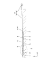
- FIG. 1 is a schematic view showing a vehicle equipped with the power storage module according to the first embodiment.
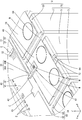
- FIG. 2 is a partial perspective view of the power storage module of the first embodiment.
- FIG. 3 is a partial plan view of the power storage module.
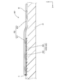
- FIG. 4 is a cross-sectional view taken along the line AA of FIG.
- FIG. 5 is an enlarged cross-sectional view of a main part of FIG.
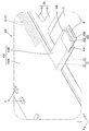
- FIG. 6 is a partial perspective view of the wiring module assembling process, and is a partial perspective view showing a state before the connection piece is placed on the connection land.
- FIG. 7 is a partial perspective view of the wiring module assembling process, and is a partial plan view showing a state before the bent portion is bent.
- FIG. 8 is a partial perspective view of the wiring module of the second embodiment.
- FIG. 1 is a schematic view showing a vehicle equipped with the power storage module according to the first embodiment.
- FIG. 2 is a partial perspective view of the power storage module of the first embodiment.
- FIG. 9 is a partial perspective view of the wiring module of the third embodiment.
- FIG. 10 is an enlarged cross-sectional view of a main part corresponding to the cross section of FIG. 5 in FIG.
- FIG. 11 is a partial perspective view of the wiring module of the fourth embodiment.
- FIG. 12 is an enlarged cross-sectional view of a main part corresponding to the cross section of FIG. 5 in FIG.
- FIG. 13 is a partial perspective view of the wiring module of the fifth embodiment.
- FIG. 14 is an enlarged cross-sectional view of a main part corresponding to the cross section of FIG. 5 in FIG.
- FIG. 15 is a partial perspective view of a wiring module that connects the FPC and the bus bar by bridging a relay member.
- a flexible resin comprising a flexible substrate, at least one bus bar, and at least one connecting piece, wherein the flexible substrate is a flexible resin in which a plurality of conductive paths containing a first metal have insulating properties. It is formed by being covered with a base material, and the bus bar is formed in a plate shape containing a second metal different from the first metal, and the conductive paths are a first conductive path and a first conductive path. It has a second conductive path extending from the path, and the resin base material has a strip-shaped main base material and a sub-base material that branches from the main base material and extends onto the bus bar.
- At least one of the first conductive paths is arranged on the base material, at least one of the second conductive paths is arranged on the sub-base material, and the second conductive path is the sub-group. It has a connecting land exposed from the material, and the connecting piece is different from the first metal and the second metal, and is welded to the second metal rather than the bonding strength in the welding of the first metal and the second metal. It is formed in a plate shape containing a third metal having a high bonding strength in the above, the bus bar is joined to the connecting piece by welding, and the connecting land is joined to the connecting piece by brazing.
- the exposed connecting lands in the sub-base material of the flexible substrate extend over the bus bar, and the connecting lands and bus bars are joined in the welding with the second metal rather than the joining strength in the welding between the first metal and the second metal. It is joined via a connecting piece formed containing a high-strength tertiary metal. That is, the flexible substrate and the bus bar can be electrically connected while improving the bonding strength in welding the bus bar and the connecting piece.
- welding in the present specification is to melt at least one base material of two base materials and integrate them so as to have continuity between the two base materials. Different joining means. Specific means of welding include, for example, laser welding, resistance welding, ultrasonic welding and the like.
- the second conductive path can be arranged between the flexible substrate and the bus bar by bending the sub-base material.
- the connection land and the bus bar can be connected without having to align the flexible substrate and the bus bar in advance. That is, unlike the case where a relay member is bridged between the flexible substrate and the bus bar to connect the flexible substrate and the bus bar, for example, the connection piece does not tilt between the connection land and the bus bar. , It is possible to prevent the joint strength between the connection land and the bus bar and the connection piece from being lowered.
- connection land arranged on the bus bar and the bus bar are connected via the connection piece, the size of the connection piece is larger than, for example, when a relay member is bridged between the flexible substrate and the bus bar. Can be reduced and the manufacturing cost can be reduced.
- connection piece has a land connection portion and a bus bar connection portion
- the third metal is a metal in which an oxide film is less likely to be formed on the surface than the second metal.
- the land connection portion is joined to the connection land by brazing
- the bus bar connection portion is joined to the bus bar by welding.
- brazing means that a filler material such as a brazing material or solder is melted and integrated so that there is continuity between the two base materials without melting the base material. For example, brazing, Brazing and the like can be mentioned.
- the joint strength in welding between the bus bar and the bus bar connection portion can be increased by forming the connection piece with the same metal as the bus bar.
- the bonding strength between the land connection portion and the connection land is lowered unless the oxide film is removed from the bonding by brazing.
- the connection piece is formed by containing a third metal, which is more difficult to form an oxide film than Basba, the land connection portion and the connection land are joined by waxing without the treatment of removing the oxide film. The strength can be increased.
- connection piece and the connection land, and the connection piece and the bus bar can be individually joined without aligning the connection pieces with respect to the two members. That is, for example, as compared with the case where the connection pieces are joined to the two members at the same time, the positional deviation of the connection pieces with respect to the connection land and the bus bar can be suppressed, and the joint strength of the joint portion is lowered due to the positional deviation. Can be suppressed.
- the first metal is copper, the second metal is aluminum, and the third metal is nickel.
- the first metal is aluminum, the second metal is copper, and the third metal is nickel.
- copper or a copper alloy is used for the conductive path and bus bar of a flexible substrate such as a flexible printed circuit board or a flexible flat cable.
- aluminum or aluminum alloy has been studied as a metal used for a flexible printed circuit board, a conductive path of a flexible flat cable, and a bus bar.
- the present inventors have found that the bonding strength between nickel and copper and the bonding strength between nickel and aluminum are higher than the bonding strength between copper and aluminum. That is, since the connection piece is formed containing nickel, the joint strength in the brazing joint between the connection land and the land connection portion is improved, and the joint strength in the weld joint between the bus bar and the bus bar connection portion is improved. Can be done.
- the connecting land is formed so as to be exposed on the surface of the sub-base material on the bus bar side, and the land connecting portion is arranged between the connecting land and the bus bar.
- the connecting portion is arranged so as to be exposed from the sub-base material.
- the bus bar connection can be welded to the bus bar using the part exposed from the sub-base material as a mark. Therefore, it is possible to prevent the joint position at the bus bar connection portion from being displaced with respect to the bus bar. As a result, it is possible to prevent the joint strength between the bus bar connection portion and the bus bar from being lowered due to the misalignment of the joint portion.
- the connecting land when the connecting land is exposed on the surface of the sub-base material opposite to the bus bar side, the position of the connecting land and the position of the bus bar are displaced in the thickness direction of the flexible substrate. It ends up. Therefore, it is necessary to process the connection piece in order to align the land connection portion and the bus bar connection portion.
- the position of the land connection portion and the position of the bus bar connection portion do not deviate in the thickness direction of the flexible substrate, so that the flexible substrate and the bus bar are electrically connected without processing the connection piece. Can be connected.
- the main base material has a bent portion that is bent toward the sub base material and is connected to the sub base material.
- a part of the main base material is bent to form the sub base material. Therefore, the yield of the flexible substrate can be improved as compared with the case where the sub-base material forms the flexible substrate protruding from the main base material from the beginning.
- connection piece and the electronic component are arranged on the connection land, the electronic component is arranged on the first conductive path, and the flexible substrate is passed through the reflow furnace. Are collectively connected to the flexible substrate. Then, by forming the bent portion, the connecting piece is arranged between the connecting land and the bus bar. That is, since the connection piece and the electronic component can be solder-bonded together, the work man-hours can be reduced and the manufacturing cost can be reduced as compared with the case where the connection piece and the electronic component are individually solder-bonded, for example.
- connection land is formed so as to be exposed on the surface of the sub-base material on the bus bar side, and the surface of the bus bar connection portion is recessed on the side opposite to the bus bar and the surface on the bus bar side. Projects toward the bus bar.
- the bus bar connection can be welded to the bus bar using the recessed part as a mark. Therefore, it is possible to prevent the joint position at the bus bar connection portion from being displaced with respect to the bus bar. As a result, it is possible to prevent the joint strength between the bus bar connection portion and the bus bar from being lowered due to the misalignment of the joint portion.
- the sub-base material has a base material through hole penetrating in the plate thickness direction, and the connecting land penetrates in the plate thickness direction and is arranged coaxially with the base material through hole. It has a through hole, and the bus bar connection portion is exposed through the base material through hole and the land through hole.
- the bus bar connection portion can be welded to the bus bar by using the portion exposed from the base material through hole and the land through hole as a mark. Therefore, it is possible to prevent the joint position at the bus bar connection portion from being displaced with respect to the bus bar. As a result, it is possible to prevent the joint strength between the bus bar connection portion and the bus bar from being lowered due to the misalignment of the joint portion.
- a plurality of power storage elements having electrode terminals are arranged in a state of holding the connection structure between the flexible substrate and the bus bar, and at least one flexible substrate and the plurality of bus bars.
- the bus bar is provided with an insulating protector attached to the power storage element group, and the bus bar is joined to the electrode terminal by welding.
- the wiring module is a wiring module for a vehicle that is mounted on a vehicle and used.
- the power storage module includes the wiring module and the power storage element group.
- connection structure between the flexible substrate and the bus bar of the present disclosure, the wiring module, and the power storage module will be described with reference to the following drawings. It should be noted that the present disclosure is not limited to these examples, and is indicated by the scope of claims, and is intended to include all modifications within the meaning and scope equivalent to the scope of claims.
- the first embodiment to which the present disclosure is applied to the storage pack 2 mounted on the vehicle 1 will be described with reference to FIGS. 1 to 7.
- the power storage pack 2 is mounted on a vehicle 1 such as an electric vehicle or a hybrid vehicle and is used as a drive source for the vehicle 1.
- vehicle 1 such as an electric vehicle or a hybrid vehicle
- the reference numerals of other members may be omitted.
- a power storage pack 2 is arranged near the center of the vehicle 1.
- a PCU 3 Power Control Unit
- the power storage pack 2 and the PCU 3 are connected by a wire harness 4.
- the power storage pack 2 and the wire harness 4 are connected by a connector (not shown).
- the power storage pack 2 has a power storage module 10 including a plurality of power storage elements 71.
- the power storage module 10 includes a power storage element group 70 and a wiring module 20. 2 and 3 show a part of the power storage module 10.
- the power storage element group 70 includes a plurality of power storage elements 71 arranged in the front-rear direction.
- Each power storage element 71 is, for example, a secondary battery.
- a pair of electrode terminals 73 are arranged at positions on the upper surface of each power storage element 71 near both ends in the left-right direction. The right electrode of the electrode terminals 73 is omitted in the figure.
- the two power storage elements 71 adjacent to each other in the front-rear direction are arranged so that the polarities of the adjacent electrode terminals 73 are different.
- the electrode terminal 73 is formed flat so that the bus bar 21 of the wiring module 20 described later can be mounted.
- the wiring module 20 is attached to the power storage element group 70 from above, and includes a bus bar 21, a flexible printed circuit board (an example of a "flexible board") 30, a bus bar 21, and a flexible printed circuit board 30.
- the connection piece 50 for connecting the above and the insulation protector 60 are provided.
- bus bar 21 As shown in FIG. 3, the bus bar 21 is formed into a flat plate having a rectangular shape in a plan view by processing a conductive metal plate material.
- the bus bar 21 is formed by processing a metal plate material containing aluminum such as aluminum and an aluminum alloy.
- the bus bar 21 is formed in a size that covers the electrode terminals 73 adjacent to each other in the front-rear direction in the power storage element group 70.
- the bus bar 21 is placed on the electrode terminals 73 so as to straddle the electrode terminals 73 adjacent to each other in the front-rear direction.
- the bus bar 21 mounted on the electrode terminal 73 is joined to the electrode terminal 73 in a circular shape by laser welding.
- a circular welding mark M is formed on the bus bar 21.
- the bus bar 21 and the electrode terminal 73 are electrically connected and fixed to each other. The laser welding may be performed linearly instead of circularly.
- the bus bar 21 and the electrode terminal 73 are formed by melting the bus bar 21 which is the base material of at least one of the bus bar 21 and the electrode terminal 73. Are integrated so that there is continuity.
- the flexible printed circuit board (hereinafter, also simply referred to as “FPC”) 30 is a member for electrically connecting a bus bar 21 and an electronic control unit (not shown) and transmitting current, temperature, and voltage applied to the bus bar 21 to the ECU.
- the electronic control unit is equipped with a microcomputer, electronic elements, etc., and is used to detect the voltage, current, temperature, etc. of the power storage element 71 transmitted through the FPC 30, and to control the charge / discharge of the power storage element group 70. It is a well-known one with the functions of.
- the FPC 30 includes a main board 30A extending in the front-rear direction over the entire length of the power storage element group 70 along the front-rear direction which is the arrangement direction of the power storage elements 71, and a left side from the main board 30A. It has a sub-board 30B protruding toward. Further, the FPC 30 includes an insulating film (an example of a “resin base material”) 40, a plurality of conductive paths 31, and an electronic component E.
- insulating film an example of a “resin base material”
- the insulating film 40 is made of a synthetic resin such as polyimide having flexibility and insulating properties, and covers the conductive path 31 from both sides in the vertical direction. As shown in FIGS. 2 and 3, the insulating film 40 has a main film portion (an example of a “main base material”) 41 and a sub film portion (an example of a “sub base material”) 46. ..
- the main film portion 41 is formed so as to extend in a band shape in the front-rear direction over the entire length of the power storage element group 70 along the front-rear direction which is the arrangement direction of the power storage elements 71.
- the main film portion 41 constitutes the main substrate 30A together with the first conductive paths 32 of the plurality of conductive paths 31 described later.
- An electronic component E is mounted on the main film portion 41. Although not shown in detail, the electronic component E is electrically connected to the first conductive path 32 of the conductive path 31, which will be described later, by soldering. As the electronic component E, any electronic component such as a resistor, a capacitor, a transistor, or a microcomputer is appropriately selected.
- a sub-film portion 46 is formed at the left end portion of the main film portion 41 so as to project to the left from the main film portion 41 by making a notch and bending the notched portion to the left. There is.
- the bent portion of the main film portion 41 is a bent portion 42 that is bent toward the left so that the portion configured as the sub film portion 46 is turned upside down. Therefore, as shown in FIGS. 2 and 3, a notch 43 having substantially the same size as the sub film portion 46 is formed at the left end portion of the main film portion 41.
- the notch 43 is formed in an L-shape in a plan view extending in the front-rear direction and extending to the right, and a bent portion 42 is formed at the rear end of the notch 43.
- Sub-film section 46 As shown in FIGS. 2 and 3, the sub-film portion 46 is formed so as to extend to the left from the bent portion 42 of the main film portion 41.
- the sub-film portion 46 constitutes the sub-board 30B together with the second conductive path 33 of the conductive path 31 described later.
- the left end portion of the sub-board 30B is a bus bar arrangement portion 47 formed in a square shape in a plan view.
- the sub-film portion 46 is arranged so as to bridge between the main substrate 30A and the bus bar 21. In other words, the sub-film portion 46 arranges the second conductive path 33 from the main substrate 30A toward the bus bar 21 so as to bridge between the main board 30A and the bus bar 21.
- a rectangular base material through hole 48 that penetrates the sub-film portion 46 in the vertical direction, which is the plate thickness direction, is formed in the central portion of the bus bar arrangement portion 47.
- the plurality of conductive paths 31 are formed of metal foils, each of which has conductivity.
- the metal foil is formed of a metal foil containing copper such as copper and a copper alloy.
- Each of the conductive paths 31 includes a first conductive path 32 and a second conductive path 33.
- the first conductive path 32 is formed so as to extend in the front-rear direction in the main film portion 41 of the main substrate 30A.
- a plurality of first conductive paths 32 in the main substrate 30A are arranged side by side at intervals in the left-right direction. 2 and 3 show only the first conductive path 32 arranged at the left end of the main substrate 30A, and are not shown except for a part of the other first conductive path 32.
- the first conductive path 32 is partially exposed by removing the main film portion 41 arranged above the first conductive path 32, and the electronic component E is exposed in the exposed portion. It is joined by solder.
- the second conductive path 33 is formed so as to extend left and right in the sub film portion 46 of the sub substrate 30B from the front end portion of the first conductive path 32 toward the left. There is.
- the second conductive path 33 is arranged between the main substrate 30A and the bus bar 21 by being supported by the sub-film portion 46.
- the left end of the second conductive path 33 is a connecting land 34.
- connection land 34 is arranged in the bus bar arrangement portion 47 of the sub-board 30B as shown in FIGS. 2 to 5.
- the connection land 34 is formed by removing the sub-film portion 46 arranged below the second conductive path 33 (on the bus bar 21 side). Therefore, the connection land 34 is exposed downward from the sub-film portion 46.
- the outer shape of the connecting land 34 is formed in a square in a plan view slightly smaller than the bus bar arrangement portion 47.
- a land through hole 35 having the same shape as the base material through hole 48 of the sub-film portion 46 and having a coaxial arrangement communicates with the base material through hole 48. It is formed so as to penetrate in the vertical direction. Therefore, the connecting land 34 is formed in a square frame shape in a plan view.
- connection piece 50 As shown in FIGS. 4 and 5, the connection piece 50 electrically connects the connection land 34 and the bus bar 21 between the bus bar arrangement portion 47 and the bus bar 21 in the sub-board 30B. In other words, the connection land 34 and the bus bar 21 are electrically connected via the connection piece 50.
- the connecting piece 50 is formed into a flat plate shape having a square planar shape by processing a conductive metal plate material.
- the connection piece 50 is formed by processing a metal plate material containing nickel such as nickel and a nickel alloy.
- the connection piece 50 is formed to have a size slightly smaller than the connection land 34 in the FPC 30.
- the connection piece 50 includes a land connection portion 52 joined to the connection land 34 and a bus bar connection portion 54 joined to the bus bar 21.
- the land connecting portion 52 is formed in a square frame shape in a plan view at the outer peripheral edge portion of the connecting piece 50.
- the land connection portion 52 is formed to have a size slightly smaller than that of the connection land 34. Therefore, when the connection piece 50 is arranged below the land connection portion 52, the land connection portion 52 is arranged slightly inside the connection land 34 as shown in FIGS. 4 and 5.
- the land connection portion 52 is joined to the connection land 34 by soldering. In a state where the land connecting portion 52 and the connecting land 34 are solder-bonded, a fillet-shaped solder fillet S is formed between the outer peripheral edge of the land connecting portion 52 and the connecting land 34.
- connection land 34 and the land connection portion 52 are integrally joined by the solder fillet S and are electrically connected.
- joining by solder is one means of brazing
- the land connecting portion 52 and the connecting land 34 are joined by solder that is melted without melting the base material such as the land connecting portion 52 and the connecting land 34. It is to integrate (two base materials) so that there is continuity.
- bus bar connection portion 54 As shown in FIGS. 2 and 3, the bus bar connection portion 54 is formed in a square shape at the center of the connection piece 50.
- the bus bar connection portion 54 is formed to have the same size as the base material through hole 48 and the land through hole 35 in the sub-board 30B. Therefore, when the connection piece 50 is arranged on the bus bar 21 and below the land connection portion 52, the bus bar connection portion 54 is arranged on the bus bar 21 and the base material through hole 48 and the base material through hole 48 and the connection piece 50 are arranged. It faces upward through the land through hole 35 and is exposed.
- the bus bar connection portion 54 is laser-welded to the bus bar 21 in a circular shape by irradiating a laser from above through the base material through hole 48 and the land through hole 35.
- the bus bar connection portion 54 and the bus bar 21 are integrally joined in a circular shape and are electrically connected.
- a circular welding mark M is formed on the bus bar 21.
- the bus bar connection portion 54 and the bus bar connection portion 54 which is at least one base material of the bus bar 21, are melted, and the bus bar connection portion 54 and the bus bar are formed. It is alloyed and integrated with 21 so as to have continuity.
- the portion joined by laser welding is not shown.
- the insulation protector 60 is attached to the power storage element group 70 while holding the bus bar 21 and the FPC 30 connected by the connection piece 50.
- the insulating protector 60 is made of an insulating synthetic resin. As shown in FIGS. 2 and 3, the insulation protector 60 includes a wiring holding portion 62 and a plurality of extending portions 64.
- the wiring holding portion 62 is formed so as to extend in a plate shape in the front-rear direction over the entire length of the power storage element group 70 along the arrangement direction of the power storage element 71.
- the width dimension of the wiring holding portion 62 in the left-right direction is formed wider than that of the main substrate 30A of the FPC 30. As a result, the wiring holding portion 62 can hold the main board 30A of the FPC 30 from below. Further, the width dimension of the wiring holding portion 62 is formed to be smaller than the length dimension between the pair of electrode terminals 73 of the power storage element 71.
- the wiring holding portion 62 is arranged between the pair of electrode terminals 73 on the upper surface of the power storage element 71 when the insulation protector 60 is attached to the power storage element group 70.
- the plurality of extending portions 64 are formed so as to extend in a prismatic shape in the left-right direction at the side edge portions on both sides of the wiring holding portion 62 in the left-right direction at intervals in the front-rear direction.
- the distance between the extending portions 64 arranged in the front-rear direction is set to be substantially the same as the thickness dimension of the power storage element 71 in the power storage element group 70. Therefore, each of the extension portions 64 is arranged above the boundary portion of the power storage elements 71 adjacent to each other in the front-rear direction when the insulation protector 60 is attached to the power storage element group 70.
- the extension portions 64 arranged at every other extension portion 64 arranged in the front-rear direction can support the bus bar 21 from below. Therefore, the insulation protector 60 is attached to the power storage element group 70 in a state where the FPC 30 is held by the wiring holding portion 62 and the plurality of bus bars 21 are held by the corresponding extending portions 64.
- This embodiment has the above configuration. Next, an example of the assembly procedure of the wiring module 20 will be described, and then an example of the assembly procedure of the power storage module 10 will be described.
- connection piece 50 Prior to assembling the wiring module 20, the connection piece 50 is joined to the FPC 30. As shown in FIG. 6, the FPC 30 before the connection piece 50 is joined is in a state in which the sub-board 30B is arranged in the notch 43 of the main board 30A.
- a notch is made in the main film portion 41 so as to follow the shape of the notch portion 43, and in the bus bar arrangement portion 47, the base material through hole 48 and the land through hole 48 are made. 35 is formed through. Further, in the bus bar arranging portion 47, the sub-film portion 46 above the portion configured as the connecting land 34 is removed to form the connecting land 34, and in the main substrate 30A, the first electronic component E is installed at the installation location P. 1 A part of the main film portion 41 on the conductive path 32 is removed.
- cream solder is applied to the connection land 34 and the installation location P of the electronic component E, the connection piece 50 is placed on the connection land 34, and the electronic component E is placed on the corresponding installation location P, respectively.
- the FPC 30 is passed through the reflow furnace, the cream solder is melted, the connection piece 50 and the connection land 34 are joined by solder, and the first conductive path 32 and the electronic component E are joined by solder. ..
- the sub-board 30B and the connection piece 50, and the main board 30A and the electronic component E are electrically connected.
- connection land 34 and the connection piece 50 are made of a metal containing copper or nickel, which is less likely to form an oxide film than aluminum.
- connection land 34 and the land connection portion 52 are compared with the case where a member containing aluminum is joined by soldering, for example. It is possible to improve the joining strength in solder joining with the connecting portion 52.
- the boundary portion of the main substrate 30A with the sub substrate 30B is bent in a valley fold to form the bent portion 42.
- the bent portion 42 is formed, as shown in FIGS. 2 and 3, the sub-board 30B arranged in the notch 43 is turned upside down and protrudes to the left from the main board 30A. Placed in the state. Therefore, in the FPC 30, the connection land 34 and the connection piece 50 are turned upside down to form the sub-board 30B by forming the bent portion 42.
- the sub-board 30B is initially arranged in the notch 43 of the main board 30A, and a notch is made in a part of the main film 41 to make a bent portion 42.
- the sub-film portion 46 is formed.
- the yield of the FPC 30 can be improved as compared with the case where the sub-base material forms the FPC protruding from the main base material from the beginning.
- connection piece 50 is arranged on the connection land 34, and the electronic component E is arranged on the first conductive path 32 to reflow the FPC 30.
- the connecting piece 50 and the electronic component E can be collectively connected to the FPC 30.
- the work man-hours and the manufacturing time can be reduced as compared with the case where both sides of the FPC 30 are solder-bonded.
- the FPC 30 to which the connection piece 50 is joined is completed.
- a plurality of bus bars 21 are arranged on the corresponding extension 64 of the insulation protector 60.
- the main substrate 30A is placed on the wiring holding portion 62 of the insulating protector 60, and is adhered and fixed on the wiring holding portion 62 with an adhesive or the like.
- the connection piece 50 joined to the sub-board 30B is placed on the bus bar 21.
- the height position of the bus bar 21 and the height position of the main board 30A are displaced in the vertical direction.
- the sub film portion 46 in the sub substrate 30B has flexibility. Therefore, when the connection piece 50 joined to the sub-board 30B is placed on the bus bar 21, the sub-board 30B bends and deforms to cause a vertical positional deviation between the bus bar 21 and the main board 30A. 30B can be absorbed (adjusted). Further, the vertical positional deviation between the bus bar 21 and the main substrate 30A can be absorbed (adjusted) by changing the bending angle of the bent portion 42.
- a laser is irradiated from above to the bus bar connection portion 54 through the base material through hole 48 and the land through hole 35 in the bus bar arrangement portion 47, and the bus bar connection portion 54 and the bus bar 21 are joined by laser welding.
- connection piece 50 is formed of a metal containing nickel, which has a higher bonding strength with aluminum than copper, the connection piece 50 is compared with the case where a member containing copper and a member containing aluminum are joined by laser welding. It is possible to improve the bonding strength in laser welding between the bus bar connection portion 54 and the bus bar 21.
- connection piece 50 and the bus bar 21 are electrically connected to complete the wiring module 20.
- the power storage module 10 is assembled so that the wiring module 20 is mounted on the power storage element group 70 from above.
- the wiring holding portion 62 of the insulating protector 60 is arranged between the pair of electrode terminals 73 in the power storage element 71, and the bus bar 21 is arranged and assembled so as to straddle the corresponding adjacent electrode terminals 73. Be done.
- bus bar 21 and the electrode terminal 73 are joined by laser welding by irradiating the laser from above the bus bar 21.
- the power storage module 10 in which the bus bar 21 and the electrode terminal 73 are electrically connected is completed.
- connection structure between the FPC (flexible substrate) 30 and the bus bar 21 in the wiring module 20 and the power storage module 10 of the present embodiment includes the FPC 30, at least one bus bar 21, and at least one connection piece 50.
- the FPC 30 is formed by covering a plurality of conductive paths 31 containing copper (first metal) with a flexible insulating film (resin base material) 40 having an insulating property, and the bus bar 21 is made of copper. It is formed in a plate shape containing aluminum (second metal) different from that of the above, and the conductive path 31 has a first conductive path 32 and a second conductive path 33 extending from the first conductive path 32, and is insulated.
- the film 40 has a strip-shaped main film portion 41 and a sub-film portion 46 that branches from the main film portion 41 and extends onto the bus bar 21, and the main film portion 41 has at least one first conductive path. 32 is arranged, at least one second conductive path 33 is arranged in the sub-film section 46, and the second conductive path 33 has a connection land 34 exposed from the sub-film section 46 and is connected.
- the piece 50 is formed in a plate shape containing nickel (third metal), which is different from copper and aluminum and has a higher bonding strength in welding with aluminum than the bonding strength in welding between copper and aluminum, and is formed in a plate shape. Is joined to the connecting piece 50 by welding, and the connecting land 34 is joined to the connecting piece 50 by soldering.
- copper or copper alloy is used for the conductive path and bus bar of a flexible substrate such as a flexible printed circuit board or a flexible flat cable.
- aluminum or an aluminum alloy has been studied as a metal for a conductive path and a bus bar of a flexible substrate such as a flexible printed circuit board and a flexible flat cable.
- the present inventors have found that the bonding strength between nickel and copper and the bonding strength between nickel and aluminum are higher than the bonding strength between copper and aluminum. That is, according to the present embodiment, the connection land 34 exposed in the sub-film portion 46 of the FPC 30 extends onto the bus bar 21. Then, the connection land 34 and the bus bar 21 are bonded via a connection piece 50 formed of a metal containing nickel having a high bonding strength with copper and aluminum. Therefore, according to the present embodiment, the FPC 30 and the bus bar 21 can be electrically connected while improving the joint strength between the bus bar 21 and the connecting piece 50.
- the second conductive path 33 can be arranged between the FPC 30 and the bus bar 21 by bending the sub-film portion 46.
- the connection land 34 and the bus bar 21 can be connected without aligning the FPC 30 and the bus bar 21 in advance. That is, for example, as shown in FIG. 15, unlike the case where the relay member 503 is bridged between the FPC 501 and the bus bar 502 to connect the FPC 501 and the bus bar 502, the connection land 34 and the bus bar 21 Since the connecting piece 50 is not tilted, it is possible to prevent the joint strength between the connecting land 34 and the bus bar 21 and the connecting piece 50 from being lowered.
- connection land 34 arranged on the bus bar 21 and the bus bar 21 are connected via the connection piece 50, for example, as shown in FIG. 15, a relay member 503 is bridged between the FPC 501 and the bus bar 502.
- the size of the connection piece 50 can be reduced as compared with the case. As a result, the manufacturing cost of the wiring module 20 and the power storage module 10 can be reduced.
- connection piece 50 of the present embodiment has a land connection portion 52 and a bus bar connection portion 54, and nickel is a metal in which an oxide film is less likely to be formed on the surface than aluminum, and the land connection portion 52.
- nickel is a metal in which an oxide film is less likely to be formed on the surface than aluminum
- the land connection portion 52 Is joined to the connection land 34 by soldering, and the bus bar connection portion 54 is joined to the bus bar 21 by welding.
- the joint strength in welding between the bus bar and the bus bar connection portion can be increased by forming the connection piece with the same metal as the bus bar.
- the oxide film can be destroyed by welding, but in solder bonding, the bonding strength between the land connection and the connecting land is reduced unless the oxide film is removed. Resulting in.
- connection piece 50 is formed containing nickel, which is less likely to form an oxide film than the bus bar 21, solder bonding between the land connection portion 52 and the connection land 34 is performed without removing the oxide film. Can increase the joint strength in.
- the land connection portion 52 of the connection piece 50 is previously joined to the connection land 34 of the FPC 30 by soldering, and then the bus bar connection portion 54 and the bus bar 21 are joined by welding. That is, the connection piece 50 and the connection land 34, and the connection piece 50 and the bus bar 21 can be individually joined without aligning the connection piece 50 with respect to the two members.
- the connection piece 50 is joined to the two members at the same time, the positional deviation of the connection piece 50 with respect to the connection land 34 and the bus bar 21 can be suppressed, and the joint portion due to the positional deviation can be suppressed. It is possible to suppress a decrease in the joint strength of the material.
- connection land 34 of the present embodiment is formed so as to be exposed on the lower surface (bus bar 21 side) of the sub-film portion 46, and the land connection portion 52 is formed between the connection land 34 and the bus bar 21.
- the bus bar connection portion 54 is arranged so as to be exposed from the sub-film portion 46.
- the sub-film portion 46 has a base material through hole 48 penetrating in the plate thickness direction, and the connecting land 34 penetrates in the plate thickness direction and is arranged coaxially with the base material through hole 48. It has a through hole 35, and the bus bar connection portion 54 is exposed through the base material through hole 48 and the land through hole 35.
- the bus bar connection portion 54 can be laser welded to the bus bar 21 by using the portion exposed from the sub film portion 46 as a mark through the base material through hole 48 and the land through hole 35. Therefore, it is possible to suppress the displacement of the welded portion due to laser welding, and it is possible to suppress the decrease in the joint strength between the bus bar connection portion 54 and the bus bar 21 due to the displacement of the welded portion.
- the connecting land when the connecting land is exposed on the surface of the sub-base material opposite to the bus bar side, the position of the connecting land and the position of the bus bar are in the vertical direction (the thickness direction of the FPC). It shifts to. In such a case, it is necessary to process the connection piece in order to align the land connection portion and the bus bar connection portion.
- the FPC 30 and the bus bar 21 can be electrically connected without processing the connection piece 50.
- the main film portion 41 has a bent portion 42 that is bent toward the sub film portion 46 and is connected to the sub film portion 46.
- the sub-film portion 46 can be formed by making a notch in a part of the main film portion 41 to form the bent portion 42. Therefore, for example, the yield of the FPC 30 can be improved as compared with the case where the sub-base material forms the FPC protruding from the main base material from the beginning.
- An electronic component E connected to the first conductive path 32 by solder is attached to the upper surface (opposite side to the bus bar 21 side) of the main film portion 41, and the bent portion 42 inverts the connection land 34. It is bent to make it.
- the connecting land 34 When the connecting land 34 is inverted to form the bent portion 42, the connecting land 34 is exposed on the upper side where the electronic component E is arranged in the state before the bent portion 42 is formed. Therefore, before forming the bent portion 42, the connection piece 50 is arranged on the connection land 34, the electronic component E is arranged on the first conductive path 32, and the FPC 30 is passed through the reflow furnace to pass the connection piece. The 50 and the electronic component E are collectively connected to the FPC 30. Then, by forming the bent portion 42, the connecting piece 50 is arranged between the connecting land 34 and the bus bar 21.
- connection piece 50 and the electronic component E can be connected to the FPC 30, so that the work man-hours can be reduced.
- the manufacturing cost of the wiring module 20, and thus the power storage module 10 can be reduced.
- the wiring module 20 is a wiring module 20 for a vehicle mounted on and used in a vehicle 1.
- the wiring module 120 in the second embodiment is a modification of the shape of the FPC 30 in the first embodiment, and the configuration, operation, and effect common to the first embodiment are duplicated, and thus the description thereof will be omitted. Further, the same reference numerals are used for the same configurations as in the first embodiment.
- the sub-board 130B is directly formed on the side edge of the main board 130A. Therefore, the sub-board 130B of the present embodiment is formed by extending the sub-board 130B from the side edge of the main board 130A toward the bus bar 21 to the left without forming the bent portion 42 as in the first embodiment. ing.
- the connection land 134 in the bus bar arrangement portion 147 is formed downward by removing the sub-film portion 146 below the connection land 34 in the bus bar arrangement portion 147.
- a connection piece 50 is solder-bonded from below to the connection land 134 exposed downward.
- the bus bar arranging portion 47 of the sub-board 130B can be arranged on the bus bar 21 without performing the work of bending a part of the FPC 130.
- the sub-board 130B can absorb the positional deviation between the main board 130A and the bus bar 21 in the height direction (vertical direction) by bending the sub-film portion 146 in the plate thickness direction (vertical direction). ..
- the wiring module 220 in the third embodiment is a modification of the shape of the bus bar arrangement portion 47 of the FPC 130 and the configuration of the connection piece 50 in the second embodiment, and has the same configurations, actions, and effects as those of the first and second embodiments. Are duplicated, so the description thereof will be omitted. Further, the same reference numerals are used for the same configurations as those of the first and second embodiments.
- the bus bar arrangement portion 247 in the FPC 230 of the third embodiment is formed in a rectangular shape so that the connection land 234 is adjacent to the left edge of the bus bar arrangement portion 247.
- the connection piece 250 the right half of the connection piece 250 is a land connection portion 252 connected to the connection land 234, and the left half of the connection piece 250 is a bus bar connection portion 254 connected to the bus bar 21.
- the land connection portion 252 is formed to be slightly smaller than the connection land 234.
- connection land 234 and the land connection portion 252 are integrally joined by the solder fillet S and are electrically connected.
- the bus bar connection portion (left half of the connection piece 250) 254 is a bus bar arrangement portion of the sub-board 230B. It is arranged on the bus bar 21 in a state of protruding to the left from 247.
- the portion of the connection piece 250 protruding to the left from the bus bar arrangement portion 247 (sub-film portion 246 of the sub-board 230A) is the bus bar connection portion 254.
- the bus bar connection portion 254 is linearly joined to the bus bar 21 in the front-rear direction by laser welding linearly from above in the front-rear direction while being arranged on the bus bar 21. As a result, a linear welding mark M is formed on the bus bar 21. That is, the bus bar connection portion 254 can be welded to the bus bar 21 by irradiating the laser with the portion exposed to the left from the bus bar arrangement portion 247 as a mark. As a result, it is possible to prevent the welded portion from being displaced. Therefore, it is possible to prevent the joint strength between the bus bar connection portion 254 and the bus bar 21 from being lowered due to the misalignment of the welded portion.
- the wiring module 320 in the fourth embodiment is a modification of the shape of the FPC 30 and the configuration of the connection piece 50 in the second embodiment, and has the same configuration, operation, and effect as those of the first and second embodiments. The description will be omitted. Further, the same reference numerals are used for the same configurations as those of the first and second embodiments.
- connection land 334 in the bus bar arrangement portion 347 of the FPC 330 of the fourth embodiment is formed upward by removing the subfilm portion 46 above the connection land 334 as shown in FIGS. 11 and 12. ing.
- the land connection portion 352 of the connection piece 350 is formed in a square frame shape in a plan view at the outer peripheral edge portion of the connection piece 350.
- the land connection portion 352 is formed to have a size slightly smaller than that of the connection land 34. Therefore, when the connection piece 350 is arranged on the land connection portion 352 and the land connection portion 352 and the connection land 334 are joined by soldering, as shown in FIG. 12, the outer peripheral edge of the land connection portion 52 and the connection land 34 A fillet-shaped solder fillet S is formed between the two. As a result, the connection land 334 and the land connection portion 352 are integrally joined by the solder fillet S and are electrically connected.
- the bus bar connection portion 354 in the connection piece 350 is formed in a circular shape at the center of the connection piece 50, as shown in FIGS. 11 and 12.
- the bus bar connection portion 354 is formed in a concave shape in which the upper surface is recessed downward and the lower surface is projected downward.
- the protruding dimension of the bus bar connecting portion 354 protruding downward from the land connecting portion 352 is set to be equal to or larger than the total thickness dimension of the connecting land 334 and the sub-film portion 346 arranged below the connecting land 334. Therefore, when the bus bar arranging portion 354 is arranged on the bus bar 21, the lower surface of the bus bar connecting portion 354 and the bus bar 21 are in surface contact with each other as shown in FIG.
- the bus bar connection portion 354 is joined to the bus bar 21 in a circular shape by laser welding from above in a circular shape while being arranged on the bus bar 21. As a result, a circular welding mark M is formed on the bus bar 21.
- connection piece 350 and the electron are arranged by arranging the connection piece 350 on the connection land 334 and the electronic component E on the first conductive path 32 and passing the FPC 330 through the reflow furnace.
- the components E can be collectively connected to the FPC 330.
- the bus bar connection portion 354 can be welded to the bus bar 21 by irradiating the connection piece 350 with a laser using the portion recessed downward as a mark. As a result, it is possible to prevent the laser irradiation location from shifting. Therefore, it is possible to prevent the joint strength between the bus bar connection portion 354 and the bus bar 21 from being lowered due to the misalignment of the welding location.
- the wiring module 420 in the fifth embodiment is a modification of the shape of the FPC 330 and the configuration of the connection piece 350 in the fourth embodiment, and the configurations, actions, and effects common to the first, second, and fourth embodiments overlap. Therefore, the description thereof will be omitted. Further, the same reference numerals shall be used for the same configurations as those of the first, second and fourth embodiments.
- the bus bar arrangement portion 447 in the FPC 430 of the fifth embodiment is formed in a rectangular shape so that the connection land 434 is adjacent to the left edge of the bus bar arrangement portion 447.
- the connection piece 450 the right half of the connection piece 450 is a land connection portion 452 connected to the connection land 434, and the left half of the connection piece 450 is a bus bar connection portion 454 connected to the bus bar 21.
- the bus bar connection portion 454 is formed in a stepped shape in which the upper surface is recessed downward and the lower surface is projected downward.
- the protruding dimension of the bus bar connecting portion 454 protruding downward from the land connecting portion 452 is set to be equal to or larger than the total thickness dimension of the connecting land 434 and the sub-film portion 446 arranged below the connecting land 434.
- the bus bar connection portion 454 is formed in a stepped shape so as to be one step lower than the land connection portion 452.
- the bus bar arranging portion 447 is arranged on the bus bar 21
- the lower surface of the bus bar connecting portion 354 and the bus bar 21 are in surface contact with each other, as shown in FIG.
- the bus bar connection portion 454 is linearly joined to the bus bar 21 in the front-rear direction by laser welding linearly from above in the front-rear direction while being arranged on the bus bar 21.
- a linear welding mark M is formed on the bus bar 21.
- connection piece 450 and the electronic component 50 are arranged on the connection land 434 and the electronic component E is arranged on the first conductive path 32, and the FPC 430 is passed through the reflow furnace.
- the components E can be collectively connected to the FPC 430.
- the bus bar connection portion 454 can be welded to the bus bar 21 by irradiating the connection piece 450 with a laser using the portion lowered below as a mark. As a result, it is possible to prevent the laser irradiation location from shifting. Therefore, it is possible to prevent the joint strength between the bus bar connection portion 454 and the bus bar 21 from being lowered due to the misalignment of the welding location.
- connection pieces 50, 150, 250, 350, 450 are formed by processing a metal plate material containing nickel such as nickel and a nickel alloy.
- a metal plate material containing nickel such as nickel and a nickel alloy.
- the present invention is not limited to this, and may be formed by a metal plate material obtained by plating the surface of aluminum, aluminum alloy, copper, copper alloy, iron or the like with nickel.
- the base material through hole 48 and the land through hole 35 are formed in a square shape.
- the present invention is not limited to this, and the base material through hole and the land through hole may be formed in a circular shape, an oval shape, a polygonal shape, or the like.
- the insulation protector 60 is configured to hold one FPC 30, 130, 230, 330, 340.
- the present invention is not limited to this, and the insulating proctor may be configured to hold a plurality of FPCs.
- the electronic component E is mounted on the FPCs 30, 130, 230, 330, and 430.
- the present invention is not limited to this, and an electronic component may not be mounted on the FPC.
- two adjacent electrode terminals 73 are connected by a bus bar 21.
- the present invention is not limited to this, and three or more electrode terminals adjacent to each other in the front-rear direction may be connected.
- a plurality of bus bars 21 and FPC30, 130, 230, 330, 340 are arranged on the insulation protector 60, and the connection piece 50 is welded to the bus bar 21 to form the wiring module 20.
- 120, 220, 320, 420 are formed.
- the wiring modules 20, 120, 220, 320, 420 are assembled to the power storage element group 70, and the bus bar 21 and the electrode terminal 73 are welded.
- the present invention is not limited to this, and an insulating protector may be arranged on the power storage element group, a bus bar and an FPC may be arranged, and the connection piece and the bus bar and the bus bar and the electrode terminal may be welded at the same time.
- the conductive path 31 in FPC30, 130, 230, 330, 340 is formed of a metal foil containing copper such as copper and a copper alloy
- the bus bar 21 is a metal plate material containing aluminum such as aluminum and an aluminum alloy.
- the structure was formed by processing.
- the present invention is not limited to this, and the conductive path may be formed of a metal foil containing aluminum such as aluminum or an aluminum alloy, and the bus bar may be formed by processing a metal plate material containing copper such as copper or a copper alloy.
- Vehicle 2 Storage pack 3: PCU 4: Wire harness 10: Power storage module 20, 120, 220, 320, 420: Wiring module 21: Bus bar 30, 130, 230, 330, 340: FPC 30A, 130A, 230A, 330A, 430A: Main board 30B, 130B, 230B, 330B, 430B: Sub-board 31: Conductive path 32: First conductive path 33: Second conductive path 34, 134, 234, 334, 434: Connection land 35: Land through hole 40: Insulating film 41: Main film part 42: Bent part 43: Notch part 46, 146, 246, 346, 446: Sub film part 47, 147, 247, 347, 447: Bus bar arrangement part 48: Base material through holes 50, 150, 250, 350, 450: Connection pieces 52, 252, 352, 452: Land connection parts 54, 254, 354, 454: Bus bar connection parts 60: Insulation protector 62: Wiring holding parts 64 : Extension 70: Power storage element group 71: Insulation
Landscapes
- Chemical & Material Sciences (AREA)
- Chemical Kinetics & Catalysis (AREA)
- Electrochemistry (AREA)
- General Chemical & Material Sciences (AREA)
- Engineering & Computer Science (AREA)
- Inorganic Chemistry (AREA)
- Microelectronics & Electronic Packaging (AREA)
- Manufacturing & Machinery (AREA)
- Connection Of Batteries Or Terminals (AREA)
- Electric Double-Layer Capacitors Or The Like (AREA)
- Electric Connection Of Electric Components To Printed Circuits (AREA)
Abstract
Priority Applications (3)
| Application Number | Priority Date | Filing Date | Title |
|---|---|---|---|
| JP2021528181A JP7124968B2 (ja) | 2019-06-21 | 2020-06-12 | 可撓性基板とバスバとの接続構造、配線モジュールおよび蓄電モジュール |
| CN202080040822.6A CN113924689B (zh) | 2019-06-21 | 2020-06-12 | 挠性基板与汇流条的连接构造、布线模块及蓄电模块 |
| US17/621,102 US12355110B2 (en) | 2019-06-21 | 2020-06-12 | Connection structure between flexible substrate and bus bar, wiring module and electricity storage module |
Applications Claiming Priority (2)
| Application Number | Priority Date | Filing Date | Title |
|---|---|---|---|
| JP2019-115250 | 2019-06-21 | ||
| JP2019115250 | 2019-06-21 |
Publications (1)
| Publication Number | Publication Date |
|---|---|
| WO2020255878A1 true WO2020255878A1 (fr) | 2020-12-24 |
Family
ID=74040764
Family Applications (1)
| Application Number | Title | Priority Date | Filing Date |
|---|---|---|---|
| PCT/JP2020/023220 Ceased WO2020255878A1 (fr) | 2019-06-21 | 2020-06-12 | Structure de connexion de substrat flexible et barre omnibus, module de câblage et module de stockage de l'électricité |
Country Status (4)
| Country | Link |
|---|---|
| US (1) | US12355110B2 (fr) |
| JP (1) | JP7124968B2 (fr) |
| CN (1) | CN113924689B (fr) |
| WO (1) | WO2020255878A1 (fr) |
Cited By (5)
| Publication number | Priority date | Publication date | Assignee | Title |
|---|---|---|---|---|
| EP4123819A3 (fr) * | 2021-06-30 | 2023-04-05 | Robert Bosch GmbH | Bloc d'accumulateur |
| JP2024013085A (ja) * | 2022-07-19 | 2024-01-31 | 矢崎総業株式会社 | 金属板の接合方法、バスバモジュールの製造方法、及び電池モジュールの製造方法 |
| JP2024013086A (ja) * | 2022-07-19 | 2024-01-31 | 矢崎総業株式会社 | 金属板と金属シートとの接合方法、バスバモジュールの製造方法、及び電池モジュールの製造方法 |
| US12002993B2 (en) | 2021-09-10 | 2024-06-04 | Milwaukee Electric Tool Corporation | Battery pack with wire bonded bus bars |
| WO2024252574A1 (fr) * | 2023-06-07 | 2024-12-12 | 株式会社オートネットワーク技術研究所 | Dispositif de circuit |
Families Citing this family (9)
| Publication number | Priority date | Publication date | Assignee | Title |
|---|---|---|---|---|
| US12315957B2 (en) * | 2021-10-01 | 2025-05-27 | Atieva, Inc. | Multi-axis ultrasonic wedge wire bonding |
| KR20240088377A (ko) * | 2022-12-13 | 2024-06-20 | 삼성에스디아이 주식회사 | 이차 전지 모듈 |
| CN116014470A (zh) * | 2022-12-29 | 2023-04-25 | 厦门市铂联科技股份有限公司 | 一种fpc与汇流排焊接方法 |
| KR20240114212A (ko) * | 2023-01-16 | 2024-07-23 | 삼성에스디아이 주식회사 | 이차 전지 모듈 |
| CN220604904U (zh) * | 2023-07-24 | 2024-03-15 | 惠州亿纬锂能股份有限公司 | 一种ccs连接片、ccs采集回路和电池包 |
| CN116845491B (zh) * | 2023-08-29 | 2023-12-22 | 深圳海辰储能控制技术有限公司 | 隔离板组件、储能装置、用电系统及储能系统 |
| DE102023135215A1 (de) * | 2023-12-14 | 2025-06-18 | Yazaki Systems Technologies Gmbh | Zellkontaktiersystem, elektrischer Energiespeicher und Verfahren zur Herstellung des Zellkontaktiersystems |
| KR20250107638A (ko) * | 2024-01-05 | 2025-07-14 | 삼성에스디아이 주식회사 | 이차전지 모듈 |
| KR20250142621A (ko) * | 2024-03-22 | 2025-09-30 | 삼성에스디아이 주식회사 | 배터리 팩 |
Citations (5)
| Publication number | Priority date | Publication date | Assignee | Title |
|---|---|---|---|---|
| JPS51134344A (en) * | 1975-05-17 | 1976-11-20 | Touwa Denshi Kk | Method of joinning alminum pipes and rods |
| JPH02256158A (ja) * | 1989-03-29 | 1990-10-16 | Asahi Chem Ind Co Ltd | 非水系電池、およびそのリードタブの溶接方法 |
| JP2011228216A (ja) * | 2010-04-22 | 2011-11-10 | Yazaki Corp | 配線材 |
| JP2012190678A (ja) * | 2011-03-11 | 2012-10-04 | Kojima Press Industry Co Ltd | 蓄電ユニット用のバスバーモジュール |
| JP2012226969A (ja) * | 2011-04-19 | 2012-11-15 | Jst Mfg Co Ltd | 電池モジュールのハーネス及び電池モジュール |
Family Cites Families (13)
| Publication number | Priority date | Publication date | Assignee | Title |
|---|---|---|---|---|
| JP3952740B2 (ja) | 2000-12-25 | 2007-08-01 | 住友化学株式会社 | 熱可塑性エラストマー組成物 |
| JP2011049158A (ja) | 2009-07-29 | 2011-03-10 | Sanyo Electric Co Ltd | バッテリモジュール、バッテリシステムおよび電動車両 |
| JP6257889B2 (ja) * | 2012-10-23 | 2018-01-10 | 日本メクトロン株式会社 | バスバー付きフレキシブルプリント配線板およびその製造方法、並びにバッテリシステム |
| JP6150904B2 (ja) * | 2013-12-25 | 2017-06-21 | 矢崎総業株式会社 | 電池配線モジュールの製造方法 |
| JP6507056B2 (ja) * | 2015-07-24 | 2019-04-24 | 株式会社オートネットワーク技術研究所 | 電池配線モジュール |
| JP6745036B2 (ja) * | 2016-07-26 | 2020-08-26 | 株式会社オートネットワーク技術研究所 | 電池用配線モジュール |
| JP6299898B1 (ja) * | 2017-02-21 | 2018-03-28 | 株式会社オートネットワーク技術研究所 | 接続モジュール |
| JP6556175B2 (ja) * | 2017-02-28 | 2019-08-07 | 矢崎総業株式会社 | 導電モジュール、及び、電池パック |
| WO2019017211A1 (fr) * | 2017-07-18 | 2019-01-24 | パナソニックIpマネジメント株式会社 | Barre omnibus et corps stratifié de batterie |
| JP2019029534A (ja) | 2017-07-31 | 2019-02-21 | イビデン株式会社 | 複合フレキシブルプリント配線板、及び、複合フレキシブルプリント配線板の製造方法 |
| JP2019029535A (ja) | 2017-07-31 | 2019-02-21 | イビデン株式会社 | フレキシブルプリント配線板、フレキシブルプリント配線板を備える電子デバイス、及び、フレキシブルプリント配線板を備える電子デバイスの製造方法 |
| JP6717788B2 (ja) * | 2017-08-04 | 2020-07-08 | 矢崎総業株式会社 | 導体モジュール |
| CN208819950U (zh) * | 2018-10-16 | 2019-05-03 | 北京长城华冠汽车科技股份有限公司 | 电池箱及具有其的电池包和车辆 |
-
2020
- 2020-06-12 US US17/621,102 patent/US12355110B2/en active Active
- 2020-06-12 WO PCT/JP2020/023220 patent/WO2020255878A1/fr not_active Ceased
- 2020-06-12 CN CN202080040822.6A patent/CN113924689B/zh active Active
- 2020-06-12 JP JP2021528181A patent/JP7124968B2/ja active Active
Patent Citations (5)
| Publication number | Priority date | Publication date | Assignee | Title |
|---|---|---|---|---|
| JPS51134344A (en) * | 1975-05-17 | 1976-11-20 | Touwa Denshi Kk | Method of joinning alminum pipes and rods |
| JPH02256158A (ja) * | 1989-03-29 | 1990-10-16 | Asahi Chem Ind Co Ltd | 非水系電池、およびそのリードタブの溶接方法 |
| JP2011228216A (ja) * | 2010-04-22 | 2011-11-10 | Yazaki Corp | 配線材 |
| JP2012190678A (ja) * | 2011-03-11 | 2012-10-04 | Kojima Press Industry Co Ltd | 蓄電ユニット用のバスバーモジュール |
| JP2012226969A (ja) * | 2011-04-19 | 2012-11-15 | Jst Mfg Co Ltd | 電池モジュールのハーネス及び電池モジュール |
Cited By (5)
| Publication number | Priority date | Publication date | Assignee | Title |
|---|---|---|---|---|
| EP4123819A3 (fr) * | 2021-06-30 | 2023-04-05 | Robert Bosch GmbH | Bloc d'accumulateur |
| US12002993B2 (en) | 2021-09-10 | 2024-06-04 | Milwaukee Electric Tool Corporation | Battery pack with wire bonded bus bars |
| JP2024013085A (ja) * | 2022-07-19 | 2024-01-31 | 矢崎総業株式会社 | 金属板の接合方法、バスバモジュールの製造方法、及び電池モジュールの製造方法 |
| JP2024013086A (ja) * | 2022-07-19 | 2024-01-31 | 矢崎総業株式会社 | 金属板と金属シートとの接合方法、バスバモジュールの製造方法、及び電池モジュールの製造方法 |
| WO2024252574A1 (fr) * | 2023-06-07 | 2024-12-12 | 株式会社オートネットワーク技術研究所 | Dispositif de circuit |
Also Published As
| Publication number | Publication date |
|---|---|
| CN113924689A (zh) | 2022-01-11 |
| JPWO2020255878A1 (fr) | 2020-12-24 |
| US12355110B2 (en) | 2025-07-08 |
| US20220344783A1 (en) | 2022-10-27 |
| CN113924689B (zh) | 2024-04-23 |
| JP7124968B2 (ja) | 2022-08-24 |
Similar Documents
| Publication | Publication Date | Title |
|---|---|---|
| JP7124968B2 (ja) | 可撓性基板とバスバとの接続構造、配線モジュールおよび蓄電モジュール | |
| US8363420B2 (en) | Electronic control apparatus | |
| CN114051675B (zh) | 配线模块及蓄电模块 | |
| CN115319282A (zh) | 激光熔接方法、熔接结构以及汇流条模块 | |
| CN115997319A (zh) | 配线模块 | |
| JP7186307B2 (ja) | 配線モジュール、端子付きフレキシブルプリント基板及び蓄電モジュール | |
| JP5540791B2 (ja) | 電子部品、電子部品を備えたインバータ装置、及び電子部品の接合方法 | |
| JP2022014957A (ja) | 電池配線モジュール | |
| JP7308281B2 (ja) | 端子付きフレキシブルプリント基板、配線モジュール及び蓄電モジュール | |
| JP3384743B2 (ja) | バスバーのレーザ溶接構造 | |
| JP7380483B2 (ja) | 車載用配線モジュール | |
| EP4138204B1 (fr) | Barre omnibus | |
| JP2024013086A (ja) | 金属板と金属シートとの接合方法、バスバモジュールの製造方法、及び電池モジュールの製造方法 | |
| JP2024013085A (ja) | 金属板の接合方法、バスバモジュールの製造方法、及び電池モジュールの製造方法 | |
| JP7727897B2 (ja) | 配線モジュール | |
| JP5857769B2 (ja) | 配線パターンの接続構造およびその製造方法 | |
| JP4514505B2 (ja) | フラット配線材 | |
| JPH10334958A (ja) | レーザ溶接構造 | |
| WO2026009581A1 (fr) | Procédé de fabrication d'ensemble carte de câblage, ensemble carte de câblage, module de câblage et module de stockage d'énergie | |
| JP3849415B2 (ja) | 導電部材及びこれと基板の接続構造 | |
| WO2024048216A1 (fr) | Carte de câblage | |
| WO2020255877A1 (fr) | Carte de circuit imprimé souple avec borne, module de câblage et module de stockage d'énergie | |
| WO2024116885A1 (fr) | Module de barre omnibus | |
| WO2024116883A1 (fr) | Module de barre omnibus | |
| JPS61294889A (ja) | 可撓性プリント基板の接続構造 |
Legal Events
| Date | Code | Title | Description |
|---|---|---|---|
| 121 | Ep: the epo has been informed by wipo that ep was designated in this application |
Ref document number: 20827083 Country of ref document: EP Kind code of ref document: A1 |
|
| ENP | Entry into the national phase |
Ref document number: 2021528181 Country of ref document: JP Kind code of ref document: A |
|
| NENP | Non-entry into the national phase |
Ref country code: DE |
|
| 122 | Ep: pct application non-entry in european phase |
Ref document number: 20827083 Country of ref document: EP Kind code of ref document: A1 |
|
| WWG | Wipo information: grant in national office |
Ref document number: 17621102 Country of ref document: US |