WO2020255880A1 - 光学素子の製造方法及び光学素子 - Google Patents
光学素子の製造方法及び光学素子 Download PDFInfo
- Publication number
- WO2020255880A1 WO2020255880A1 PCT/JP2020/023233 JP2020023233W WO2020255880A1 WO 2020255880 A1 WO2020255880 A1 WO 2020255880A1 JP 2020023233 W JP2020023233 W JP 2020023233W WO 2020255880 A1 WO2020255880 A1 WO 2020255880A1
- Authority
- WO
- WIPO (PCT)
- Prior art keywords
- element portion
- optical
- layer
- laser
- heat sink
- Prior art date
- Legal status (The legal status is an assumption and is not a legal conclusion. Google has not performed a legal analysis and makes no representation as to the accuracy of the status listed.)
- Ceased
Links
Images


Classifications
-
- H—ELECTRICITY
- H01—ELECTRIC ELEMENTS
- H01S—DEVICES USING THE PROCESS OF LIGHT AMPLIFICATION BY STIMULATED EMISSION OF RADIATION [LASER] TO AMPLIFY OR GENERATE LIGHT; DEVICES USING STIMULATED EMISSION OF ELECTROMAGNETIC RADIATION IN WAVE RANGES OTHER THAN OPTICAL
- H01S3/00—Lasers, i.e. devices using stimulated emission of electromagnetic radiation in the infrared, visible or ultraviolet wave range
- H01S3/05—Construction or shape of optical resonators; Accommodation of active medium therein; Shape of active medium
- H01S3/06—Construction or shape of active medium
-
- C—CHEMISTRY; METALLURGY
- C03—GLASS; MINERAL OR SLAG WOOL
- C03C—CHEMICAL COMPOSITION OF GLASSES, GLAZES OR VITREOUS ENAMELS; SURFACE TREATMENT OF GLASS; SURFACE TREATMENT OF FIBRES OR FILAMENTS MADE FROM GLASS, MINERALS OR SLAGS; JOINING GLASS TO GLASS OR OTHER MATERIALS
- C03C27/00—Joining pieces of glass to pieces of other inorganic material; Joining glass to glass other than by fusing
- C03C27/04—Joining glass to metal by means of an interlayer
-
- C—CHEMISTRY; METALLURGY
- C03—GLASS; MINERAL OR SLAG WOOL
- C03C—CHEMICAL COMPOSITION OF GLASSES, GLAZES OR VITREOUS ENAMELS; SURFACE TREATMENT OF GLASS; SURFACE TREATMENT OF FIBRES OR FILAMENTS MADE FROM GLASS, MINERALS OR SLAGS; JOINING GLASS TO GLASS OR OTHER MATERIALS
- C03C27/00—Joining pieces of glass to pieces of other inorganic material; Joining glass to glass other than by fusing
- C03C27/06—Joining glass to glass by processes other than fusing
-
- C—CHEMISTRY; METALLURGY
- C04—CEMENTS; CONCRETE; ARTIFICIAL STONE; CERAMICS; REFRACTORIES
- C04B—LIME, MAGNESIA; SLAG; CEMENTS; COMPOSITIONS THEREOF, e.g. MORTARS, CONCRETE OR LIKE BUILDING MATERIALS; ARTIFICIAL STONE; CERAMICS; REFRACTORIES; TREATMENT OF NATURAL STONE
- C04B37/00—Joining burned ceramic articles with other burned ceramic articles or other articles by heating
- C04B37/003—Joining burned ceramic articles with other burned ceramic articles or other articles by heating by means of an interlayer consisting of a combination of materials selected from glass, or ceramic material with metals, metal oxides or metal salts
- C04B37/005—Joining burned ceramic articles with other burned ceramic articles or other articles by heating by means of an interlayer consisting of a combination of materials selected from glass, or ceramic material with metals, metal oxides or metal salts consisting of glass or ceramic material
-
- C—CHEMISTRY; METALLURGY
- C04—CEMENTS; CONCRETE; ARTIFICIAL STONE; CERAMICS; REFRACTORIES
- C04B—LIME, MAGNESIA; SLAG; CEMENTS; COMPOSITIONS THEREOF, e.g. MORTARS, CONCRETE OR LIKE BUILDING MATERIALS; ARTIFICIAL STONE; CERAMICS; REFRACTORIES; TREATMENT OF NATURAL STONE
- C04B37/00—Joining burned ceramic articles with other burned ceramic articles or other articles by heating
- C04B37/02—Joining burned ceramic articles with other burned ceramic articles or other articles by heating with metallic articles
- C04B37/023—Joining burned ceramic articles with other burned ceramic articles or other articles by heating with metallic articles characterised by the interlayer used
- C04B37/025—Joining burned ceramic articles with other burned ceramic articles or other articles by heating with metallic articles characterised by the interlayer used consisting of glass or ceramic material
-
- H—ELECTRICITY
- H01—ELECTRIC ELEMENTS
- H01S—DEVICES USING THE PROCESS OF LIGHT AMPLIFICATION BY STIMULATED EMISSION OF RADIATION [LASER] TO AMPLIFY OR GENERATE LIGHT; DEVICES USING STIMULATED EMISSION OF ELECTROMAGNETIC RADIATION IN WAVE RANGES OTHER THAN OPTICAL
- H01S3/00—Lasers, i.e. devices using stimulated emission of electromagnetic radiation in the infrared, visible or ultraviolet wave range
- H01S3/02—Constructional details
- H01S3/04—Arrangements for thermal management
- H01S3/0405—Conductive cooling, e.g. by heat sinks or thermo-electric elements
-
- H—ELECTRICITY
- H01—ELECTRIC ELEMENTS
- H01S—DEVICES USING THE PROCESS OF LIGHT AMPLIFICATION BY STIMULATED EMISSION OF RADIATION [LASER] TO AMPLIFY OR GENERATE LIGHT; DEVICES USING STIMULATED EMISSION OF ELECTROMAGNETIC RADIATION IN WAVE RANGES OTHER THAN OPTICAL
- H01S3/00—Lasers, i.e. devices using stimulated emission of electromagnetic radiation in the infrared, visible or ultraviolet wave range
- H01S3/02—Constructional details
- H01S3/04—Arrangements for thermal management
- H01S3/042—Arrangements for thermal management for solid state lasers
-
- H—ELECTRICITY
- H01—ELECTRIC ELEMENTS
- H01S—DEVICES USING THE PROCESS OF LIGHT AMPLIFICATION BY STIMULATED EMISSION OF RADIATION [LASER] TO AMPLIFY OR GENERATE LIGHT; DEVICES USING STIMULATED EMISSION OF ELECTROMAGNETIC RADIATION IN WAVE RANGES OTHER THAN OPTICAL
- H01S3/00—Lasers, i.e. devices using stimulated emission of electromagnetic radiation in the infrared, visible or ultraviolet wave range
- H01S3/05—Construction or shape of optical resonators; Accommodation of active medium therein; Shape of active medium
- H01S3/06—Construction or shape of active medium
- H01S3/0602—Crystal lasers or glass lasers
- H01S3/0606—Crystal lasers or glass lasers with polygonal cross-section, e.g. slab, prism
-
- H—ELECTRICITY
- H01—ELECTRIC ELEMENTS
- H01S—DEVICES USING THE PROCESS OF LIGHT AMPLIFICATION BY STIMULATED EMISSION OF RADIATION [LASER] TO AMPLIFY OR GENERATE LIGHT; DEVICES USING STIMULATED EMISSION OF ELECTROMAGNETIC RADIATION IN WAVE RANGES OTHER THAN OPTICAL
- H01S3/00—Lasers, i.e. devices using stimulated emission of electromagnetic radiation in the infrared, visible or ultraviolet wave range
- H01S3/05—Construction or shape of optical resonators; Accommodation of active medium therein; Shape of active medium
- H01S3/06—Construction or shape of active medium
- H01S3/0619—Coatings, e.g. AR, HR, passivation layer
- H01S3/0621—Coatings on the end-faces, e.g. input/output surfaces of the laser light
-
- H—ELECTRICITY
- H01—ELECTRIC ELEMENTS
- H01S—DEVICES USING THE PROCESS OF LIGHT AMPLIFICATION BY STIMULATED EMISSION OF RADIATION [LASER] TO AMPLIFY OR GENERATE LIGHT; DEVICES USING STIMULATED EMISSION OF ELECTROMAGNETIC RADIATION IN WAVE RANGES OTHER THAN OPTICAL
- H01S3/00—Lasers, i.e. devices using stimulated emission of electromagnetic radiation in the infrared, visible or ultraviolet wave range
- H01S3/23—Arrangements of two or more lasers not provided for in groups H01S3/02 - H01S3/22, e.g. tandem arrangements of separate active media
-
- C—CHEMISTRY; METALLURGY
- C04—CEMENTS; CONCRETE; ARTIFICIAL STONE; CERAMICS; REFRACTORIES
- C04B—LIME, MAGNESIA; SLAG; CEMENTS; COMPOSITIONS THEREOF, e.g. MORTARS, CONCRETE OR LIKE BUILDING MATERIALS; ARTIFICIAL STONE; CERAMICS; REFRACTORIES; TREATMENT OF NATURAL STONE
- C04B2235/00—Aspects relating to ceramic starting mixtures or sintered ceramic products
- C04B2235/70—Aspects relating to sintered or melt-casted ceramic products
- C04B2235/96—Properties of ceramic products, e.g. mechanical properties such as strength, toughness, wear resistance
- C04B2235/9646—Optical properties
- C04B2235/9653—Translucent or transparent ceramics other than alumina
-
- C—CHEMISTRY; METALLURGY
- C04—CEMENTS; CONCRETE; ARTIFICIAL STONE; CERAMICS; REFRACTORIES
- C04B—LIME, MAGNESIA; SLAG; CEMENTS; COMPOSITIONS THEREOF, e.g. MORTARS, CONCRETE OR LIKE BUILDING MATERIALS; ARTIFICIAL STONE; CERAMICS; REFRACTORIES; TREATMENT OF NATURAL STONE
- C04B2237/00—Aspects relating to ceramic laminates or to joining of ceramic articles with other articles by heating
- C04B2237/02—Aspects relating to interlayers, e.g. used to join ceramic articles with other articles by heating
- C04B2237/04—Ceramic interlayers
- C04B2237/06—Oxidic interlayers
- C04B2237/062—Oxidic interlayers based on silica or silicates
-
- C—CHEMISTRY; METALLURGY
- C04—CEMENTS; CONCRETE; ARTIFICIAL STONE; CERAMICS; REFRACTORIES
- C04B—LIME, MAGNESIA; SLAG; CEMENTS; COMPOSITIONS THEREOF, e.g. MORTARS, CONCRETE OR LIKE BUILDING MATERIALS; ARTIFICIAL STONE; CERAMICS; REFRACTORIES; TREATMENT OF NATURAL STONE
- C04B2237/00—Aspects relating to ceramic laminates or to joining of ceramic articles with other articles by heating
- C04B2237/02—Aspects relating to interlayers, e.g. used to join ceramic articles with other articles by heating
- C04B2237/04—Ceramic interlayers
- C04B2237/06—Oxidic interlayers
- C04B2237/064—Oxidic interlayers based on alumina or aluminates
-
- C—CHEMISTRY; METALLURGY
- C04—CEMENTS; CONCRETE; ARTIFICIAL STONE; CERAMICS; REFRACTORIES
- C04B—LIME, MAGNESIA; SLAG; CEMENTS; COMPOSITIONS THEREOF, e.g. MORTARS, CONCRETE OR LIKE BUILDING MATERIALS; ARTIFICIAL STONE; CERAMICS; REFRACTORIES; TREATMENT OF NATURAL STONE
- C04B2237/00—Aspects relating to ceramic laminates or to joining of ceramic articles with other articles by heating
- C04B2237/02—Aspects relating to interlayers, e.g. used to join ceramic articles with other articles by heating
- C04B2237/10—Glass interlayers, e.g. frit or flux
-
- C—CHEMISTRY; METALLURGY
- C04—CEMENTS; CONCRETE; ARTIFICIAL STONE; CERAMICS; REFRACTORIES
- C04B—LIME, MAGNESIA; SLAG; CEMENTS; COMPOSITIONS THEREOF, e.g. MORTARS, CONCRETE OR LIKE BUILDING MATERIALS; ARTIFICIAL STONE; CERAMICS; REFRACTORIES; TREATMENT OF NATURAL STONE
- C04B2237/00—Aspects relating to ceramic laminates or to joining of ceramic articles with other articles by heating
- C04B2237/30—Composition of layers of ceramic laminates or of ceramic or metallic articles to be joined by heating, e.g. Si substrates
- C04B2237/32—Ceramic
- C04B2237/34—Oxidic
- C04B2237/341—Silica or silicates
-
- C—CHEMISTRY; METALLURGY
- C04—CEMENTS; CONCRETE; ARTIFICIAL STONE; CERAMICS; REFRACTORIES
- C04B—LIME, MAGNESIA; SLAG; CEMENTS; COMPOSITIONS THEREOF, e.g. MORTARS, CONCRETE OR LIKE BUILDING MATERIALS; ARTIFICIAL STONE; CERAMICS; REFRACTORIES; TREATMENT OF NATURAL STONE
- C04B2237/00—Aspects relating to ceramic laminates or to joining of ceramic articles with other articles by heating
- C04B2237/30—Composition of layers of ceramic laminates or of ceramic or metallic articles to be joined by heating, e.g. Si substrates
- C04B2237/32—Ceramic
- C04B2237/34—Oxidic
- C04B2237/343—Alumina or aluminates
-
- C—CHEMISTRY; METALLURGY
- C04—CEMENTS; CONCRETE; ARTIFICIAL STONE; CERAMICS; REFRACTORIES
- C04B—LIME, MAGNESIA; SLAG; CEMENTS; COMPOSITIONS THEREOF, e.g. MORTARS, CONCRETE OR LIKE BUILDING MATERIALS; ARTIFICIAL STONE; CERAMICS; REFRACTORIES; TREATMENT OF NATURAL STONE
- C04B2237/00—Aspects relating to ceramic laminates or to joining of ceramic articles with other articles by heating
- C04B2237/50—Processing aspects relating to ceramic laminates or to the joining of ceramic articles with other articles by heating
- C04B2237/55—Pre-treatments of a coated or not coated substrate other than oxidation treatment in order to form an active joining layer
-
- C—CHEMISTRY; METALLURGY
- C04—CEMENTS; CONCRETE; ARTIFICIAL STONE; CERAMICS; REFRACTORIES
- C04B—LIME, MAGNESIA; SLAG; CEMENTS; COMPOSITIONS THEREOF, e.g. MORTARS, CONCRETE OR LIKE BUILDING MATERIALS; ARTIFICIAL STONE; CERAMICS; REFRACTORIES; TREATMENT OF NATURAL STONE
- C04B2237/00—Aspects relating to ceramic laminates or to joining of ceramic articles with other articles by heating
- C04B2237/50—Processing aspects relating to ceramic laminates or to the joining of ceramic articles with other articles by heating
- C04B2237/72—Forming laminates or joined articles comprising at least two interlayers directly next to each other
-
- G—PHYSICS
- G02—OPTICS
- G02B—OPTICAL ELEMENTS, SYSTEMS OR APPARATUS
- G02B1/00—Optical elements characterised by the material of which they are made; Optical coatings for optical elements
- G02B1/02—Optical elements characterised by the material of which they are made; Optical coatings for optical elements made of crystals, e.g. rock-salt, semi-conductors
-
- G—PHYSICS
- G02—OPTICS
- G02B—OPTICAL ELEMENTS, SYSTEMS OR APPARATUS
- G02B6/00—Light guides; Structural details of arrangements comprising light guides and other optical elements, e.g. couplings
- G02B6/0001—Light guides; Structural details of arrangements comprising light guides and other optical elements, e.g. couplings specially adapted for lighting devices or systems
- G02B6/0011—Light guides; Structural details of arrangements comprising light guides and other optical elements, e.g. couplings specially adapted for lighting devices or systems the light guides being planar or of plate-like form
- G02B6/0065—Manufacturing aspects; Material aspects
-
- H—ELECTRICITY
- H01—ELECTRIC ELEMENTS
- H01S—DEVICES USING THE PROCESS OF LIGHT AMPLIFICATION BY STIMULATED EMISSION OF RADIATION [LASER] TO AMPLIFY OR GENERATE LIGHT; DEVICES USING STIMULATED EMISSION OF ELECTROMAGNETIC RADIATION IN WAVE RANGES OTHER THAN OPTICAL
- H01S3/00—Lasers, i.e. devices using stimulated emission of electromagnetic radiation in the infrared, visible or ultraviolet wave range
- H01S3/05—Construction or shape of optical resonators; Accommodation of active medium therein; Shape of active medium
- H01S3/06—Construction or shape of active medium
- H01S3/0602—Crystal lasers or glass lasers
- H01S3/0604—Crystal lasers or glass lasers in the form of a plate or disc
-
- H—ELECTRICITY
- H01—ELECTRIC ELEMENTS
- H01S—DEVICES USING THE PROCESS OF LIGHT AMPLIFICATION BY STIMULATED EMISSION OF RADIATION [LASER] TO AMPLIFY OR GENERATE LIGHT; DEVICES USING STIMULATED EMISSION OF ELECTROMAGNETIC RADIATION IN WAVE RANGES OTHER THAN OPTICAL
- H01S3/00—Lasers, i.e. devices using stimulated emission of electromagnetic radiation in the infrared, visible or ultraviolet wave range
- H01S3/05—Construction or shape of optical resonators; Accommodation of active medium therein; Shape of active medium
- H01S3/06—Construction or shape of active medium
- H01S3/0602—Crystal lasers or glass lasers
- H01S3/0612—Non-homogeneous structure
-
- H—ELECTRICITY
- H01—ELECTRIC ELEMENTS
- H01S—DEVICES USING THE PROCESS OF LIGHT AMPLIFICATION BY STIMULATED EMISSION OF RADIATION [LASER] TO AMPLIFY OR GENERATE LIGHT; DEVICES USING STIMULATED EMISSION OF ELECTROMAGNETIC RADIATION IN WAVE RANGES OTHER THAN OPTICAL
- H01S3/00—Lasers, i.e. devices using stimulated emission of electromagnetic radiation in the infrared, visible or ultraviolet wave range
- H01S3/05—Construction or shape of optical resonators; Accommodation of active medium therein; Shape of active medium
- H01S3/06—Construction or shape of active medium
- H01S3/0627—Construction or shape of active medium the resonator being monolithic, e.g. microlaser
-
- H—ELECTRICITY
- H01—ELECTRIC ELEMENTS
- H01S—DEVICES USING THE PROCESS OF LIGHT AMPLIFICATION BY STIMULATED EMISSION OF RADIATION [LASER] TO AMPLIFY OR GENERATE LIGHT; DEVICES USING STIMULATED EMISSION OF ELECTROMAGNETIC RADIATION IN WAVE RANGES OTHER THAN OPTICAL
- H01S3/00—Lasers, i.e. devices using stimulated emission of electromagnetic radiation in the infrared, visible or ultraviolet wave range
- H01S3/05—Construction or shape of optical resonators; Accommodation of active medium therein; Shape of active medium
- H01S3/06—Construction or shape of active medium
- H01S3/07—Construction or shape of active medium consisting of a plurality of parts, e.g. segments
-
- H—ELECTRICITY
- H01—ELECTRIC ELEMENTS
- H01S—DEVICES USING THE PROCESS OF LIGHT AMPLIFICATION BY STIMULATED EMISSION OF RADIATION [LASER] TO AMPLIFY OR GENERATE LIGHT; DEVICES USING STIMULATED EMISSION OF ELECTROMAGNETIC RADIATION IN WAVE RANGES OTHER THAN OPTICAL
- H01S3/00—Lasers, i.e. devices using stimulated emission of electromagnetic radiation in the infrared, visible or ultraviolet wave range
- H01S3/14—Lasers, i.e. devices using stimulated emission of electromagnetic radiation in the infrared, visible or ultraviolet wave range characterised by the material used as the active medium
- H01S3/16—Solid materials
- H01S3/163—Solid materials characterised by a crystal matrix
Definitions
- One aspect of the present invention relates to a method for manufacturing an optical element through which laser light is transmitted, reciprocated or reflected, and the optical element thereof.
- the first element portion and the second element portion are made of different materials, they can be joined via the amorphous layer as described above.
- the amorphous layer is in a metastable state, the material state (bonded state) of the optical element becomes unstable, and for example, the strength such as the optical resistance of the optical element may be insufficient.
- One aspect of the present invention has been made in view of the above circumstances, and an object of the present invention is to provide a method for manufacturing an optical element and an optical element capable of stabilizing the substance state.
- the method for manufacturing an optical element is a method for manufacturing an optical element that transmits, reciprocates, or reflects laser light, and the first element portion and the second element portion that are transparent to the laser light are A first step of obtaining a bonding element formed by surface-active bonding via an amorphous layer, and after the first step, the temperature of the bonding element is raised to crystallize at least a part of the amorphous layer.
- the junction element is heated to a predetermined temperature lower than the melting point of the first element portion and the second element portion in the second step.
- the amorphous layer is epitaxially grown by raising the temperature of the bonded element, and at least a part of the amorphous layer is crystallized to form a material state (bonded state) of the optical element. ) Can be stabilized.
- ions are formed on at least one of the surface on the junction side of the first element portion and the surface on the junction side of the second element portion in a substantially vacuum environment.
- a bonding element may be obtained by irradiating a beam or a high-speed atomic beam and then bringing the surface of the first element portion into contact with the surface of the second element portion.
- the amorphous layer uses an ion beam or a high-speed atomic beam as impurities other than the substances constituting the first element portion and the second element portion. It may contain at least one of the constituent beam source elements and the beam housing material constituting the beam housing of the ion beam or the high-speed atomic beam.
- the temperature of the bonded element is raised, there is a concern that stress is generated in the bonded portion due to the difference in the coefficient of linear expansion, and damage such as peeling occurs in the optical element.
- the amorphous layer contains a beam source element and / or a beam housing material as impurities
- the temperature required for epitaxial growth at the time of temperature rise is set higher than the melting points of the first element portion and the second element portion. It is found that it can be lowered to a lower predetermined temperature. Therefore, in the method for manufacturing an optical element according to one aspect of the present invention, the amorphous layer contains a beam source element and / or a beam housing material, and the temperature of temperature rise is the melting point of the first element portion and the second element portion. It has been lowered to a lower predetermined temperature. Thereby, the damage of the optical element can be suppressed.
- the first element portion is made of diamond, silicon carbide, sapphire, garnet containing YAG, vanadate, sex oxide, flolide, apatite, tongue state, silicate, and phosphoric acid.
- a material, a laser material to which a rare earth ion or a transition metal is added, an optical switch material, a nonlinear optical material, or a functional optical material, and the second element part is a garnet containing diamond, silicon carbide, sapphire, YAG, vanadate, etc.
- the predetermined temperature may be 100 ° C. or higher and lower than the melting point of the substance constituting the amorphous layer. In this case, it is possible to stabilize the material state of the optical element by raising the temperature of the optical element including the first element portion and the second element portion.
- YAG is garnet, YSAG, YGAG, GGG, GSGG , LuAG, oxides such as YALO, vanadates, for example YVO 4 or GdVO 4, LuVO VO 4 compounds such as 4, Sexton oxide is Y 2 O 3, Sr 2 O 3 , Lu 2 O 3 , fluorides such as YLF, SrF 2 , CaF 2 for floride, phosphate calcium compounds such as FAP, SFAP, VAP, SVAP for apatite, KYW, KGW etc. for tongue state It is a WO 4 compound.
- the functional optical material is, for example, a material having a non-linear sensitivity, an electro-optical effect, and a magneto-optical effect, such as crystal, LBO, LiNbO 3 , KTiPO 4 , ZGP, GaAs or GaP, ZnSe, ZnS.
- the ceramics include those having a Faraday effect such as TGG (terbium gallium garnet), TAG (terbium aluminum garnet), and TSAG (terbium scandium aluminum garnet) ceramics.
- the state of the first element portion and the second element portion may be single crystal, amorphous (including glass), or ceramics.
- At least one of the first element portion and the second element portion has an optical coating layer on the junction side portion thereof, and a predetermined temperature is 100 ° C. or higher and 600 ° C. or lower. It may be. This makes it possible to suppress damage to the optical coating layer.
- the flatness of the interface of the crystallized layer obtained by crystallizing the amorphous layer in the second step is higher than the flatness of the interface of the amorphous layer. It may be expensive. This makes it possible to suppress the possibility of adverse effects of the interface on the transmitted, reciprocating or reflected laser light.
- the optical element according to one aspect of the present invention is an optical element that transmits, reciprocates, or reflects laser light, and is a first element portion and a second element portion that are transparent to the laser light, and a first element portion and a first element portion.
- a crystallization layer interposed between the two element portions and crystallized is provided, and the crystallization layer forms the first element portion in a 10 nm region from the first element portion side to the second element portion side.
- the constituent elements are continuously replaced with the constituent elements of the second element portion.
- the optical element according to one aspect of the present invention is an optical element that transmits, reciprocates, or reflects laser light, and includes a first element portion and a second element portion that are transparent to the laser light, and a first element portion and a first element portion.
- a crystallization layer interposed between the two element portions and crystallized is provided, and the crystallization layer contains at least one of Ar, Ne, Xe, He, Fe, Ni and Cr.
- a crystallized layer is interposed between the first element portion and the second element portion, not an amorphous layer.
- the crystallized layer contains at least one of Ar, Ne, Xe, He, Fe, Ni and Cr. Therefore, it is advantageous for recrystallization (not only is it easy to recrystallize in a low temperature temperature rise treatment due to the inclusion of a small amount of impurities, but also in a short time if the temperature rise treatment is at a normal temperature. Is possible).
- the optical element according to one aspect of the present invention is an optical element that transmits, reciprocates, or reflects laser light, and includes a first element portion and a second element portion that are transparent to the laser light, and a first element portion and a first element portion.
- a crystallized layer interposed between the two element portions and crystallized is provided, and at least one of the first element portion and the second element portion has an optical coating layer on the junction side portion thereof and is optically coated.
- the elements constituting the first element portion or the second element portion in the 10 nm region are continuously exchanged with the elements constituting the optical coating layer. ..
- At least one of the first element portion and the second element portion has an optical coating layer on the junction side portion thereof, and the crystallization layer is Ar, Ne, Xe, He, It may contain at least one of Fe, Ni and Cr.
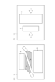
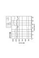
- FIG. 1 is a schematic perspective view showing a small integrated laser device including the laser element according to the embodiment.
- FIG. 2A is a diagram illustrating a method for manufacturing a laser element according to an embodiment.
- FIG. 2B is a diagram illustrating a continuation of FIG. 2A.
- FIG. 3A is a diagram illustrating a continuation of FIG. 2B.
- FIG. 3B is a diagram illustrating a continuation of FIG. 3A.
- FIG. 4 is a diagram illustrating a continuation of FIG. 3 (b).
- FIG. 5A is a diagram showing the periphery of the junction portion of the junction element according to the embodiment.
- FIG. 5B is an enlarged view showing the inside of the broken line frame of FIG. 5A.
- FIG. 6A is a diagram showing the periphery of the joint portion of the laser element according to the embodiment.
- FIG. 6B is an enlarged view showing the inside of the broken line frame of FIG. 6A.
- FIG. 7A is a diagram showing the periphery of the junction portion of the junction element according to the embodiment.
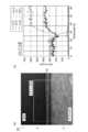
- FIG. 7B is a graph showing the elements detected within the frame of FIG. 7A.
- FIG. 8A is a diagram showing the periphery of the joint portion of the laser element according to the embodiment.
- FIG. 8B is a graph showing the elements detected in the frame of FIG. 8A.
- FIG. 9A is a diagram showing the periphery of the joint portion of the laser element according to the embodiment.
- FIG. 9B is a graph showing the elements detected in the frame of FIG. 9A.
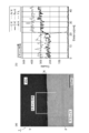
- FIG. 10A is a diagram showing the periphery of the joint portion of the laser element according to the embodiment.
- FIG. 10B is a graph showing the elements detected within the frame of FIG. 10A.
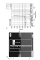
- FIG. 11A is a diagram showing the periphery of the joint portion of the laser element according to the embodiment.
- FIG. 11B is a graph showing the elements detected in the frame of FIG. 11A.
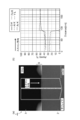
- FIG. 12 is a diagram showing the periphery of the junction portion of the junction element according to the embodiment.
- FIG. 13 is a diagram showing the periphery of the joint portion of the laser element according to the embodiment.
- FIG. 14 is a diagram showing the periphery of the joint portion of the laser element according to the embodiment.
- FIG. 15 is a cross-sectional view showing a laser element according to a modified example.
- FIG. 16 is a diagram showing the periphery of the junction portion of the junction element, which is an element before the temperature rise step.
- FIG. 17 is a diagram showing the periphery of the joint portion of the laser element, which is the element after the temperature raising step.
- FIG. 18 is a diagram showing the periphery of the joint portion of the laser element, which is the element after the temperature raising step.
- FIG. 19 is a graph showing the elements detected at the positions shown in FIG. 18 in the scanning direction.
- FIG. 20 is a diagram showing the periphery of the junction portion of the junction element, which is an element before the temperature rise step.
- FIG. 21 is a graph showing the elements detected at the positions shown in FIG. 20 in the scanning direction.
- FIG. 22 is a diagram showing the periphery of the junction portion of the junction element after the EB irradiation, which is the element before the temperature rise step.
- FIG. 1 is a schematic perspective view showing a small integrated laser device 100.
- the compact integrated laser device 100 shown in FIG. 1 is a laser light source that emits laser light L, and constitutes a power laser that is smaller, simpler, and has higher output than a fiber laser or a disk laser.
- the small integrated laser device 100 includes the laser element 1 according to the embodiment.
- the emission direction (traveling direction) of the laser beam L will be described as the “Z direction”.
- the cross section shown in FIGS. 2 and 2 is an XY cross section, and the in-plane horizontal axis is the “X direction” and the in-plane vertical axis is the “Y direction”.
- the dimensional ratios in the drawings are not limited to the ratios shown.
- the laser element 1 is an optical element having a DFC structure.
- the laser element 1 includes a plurality of heat sinks 2, a plurality of laser media 3, a first coating layer 4a, a second coating layer 5, and a third coating layer 4b.
- the laser element 1 can form a high-power microlaser.
- the laser element 1 when the diode light of continuous oscillation having a wavelength of 808 nm is input as the excitation light I from one end side (left side in the drawing) in the Z direction along the Z direction, the laser light L having a wavelength of 1064 nm is generated. It is emitted from the other end side (right side in the drawing) in the Z direction via the Q-switch element 8 made of a saturable absorber.
- the laser element 1 is not provided with the Q-switch element 8, it is possible to configure a CW (Continuous Wave) laser.
- the heat sink 2 and the laser medium 3 have a rectangular plate shape with the Z direction as the thickness direction.
- the heat sink 2 has a flat plate shape having a thickness of 1 mm, a vertical dimension of 10 mm, and a horizontal dimension of 10 mm.
- the laser medium 3 has a flat plate shape having a thickness of 1 mm, a vertical dimension of 8 mm, and a horizontal dimension of 8 mm.
- the heat sink 2 and the laser medium 3 may have a circular plate shape.
- the heat sink 2 and the laser medium 3 are arranged so as to be alternately arranged along the Z direction. That is, the laser medium 3 is located between the pair of adjacent heat sinks 2.
- the heat sink 2 and the laser medium 3 are joined (directly joined) without using an adhesive.
- the portion from the laser medium 3 arranged on the one end side to the laser medium 3 arranged on the other end side in the Z direction functions as a resonator.
- the heat sink 2 is a substance having a thermal conductivity similar to or higher than that of the laser medium 3.
- the heat sink 2 has a function of dissipating heat from the laser medium 3.
- the heat sink 2 constitutes the first element portion.
- the heat insulating material 2 is a garnet containing diamond, silicon carbide, sapphire, YAG, vanadate, sex oxide, floride, apatite, tongue state, silicate, phosphoric acid-based material, laser material to which rare earth ion or transition metal is added, and optical switch material. , Non-linear optical material, or functional optical material.
- the vanadate is, for example, YVO 4 or LuVO 4 .
- the heat sink 2 is an example of the first element portion, and the first element portion is not limited to the heat sink 2.
- the state of the first element unit may be single crystal, amorphous (including glass), or ceramics.
- the laser medium 3 is a substance that amplifies light in an excited state by forming a population inversion that exceeds the loss and amplifies light by utilizing stimulated emission.
- the laser medium 3 is also referred to as a gain medium.
- the laser medium 3 constitutes a second element unit.
- the laser medium 3 includes diamond, silicon carbide, sapphire, garnet containing YAG, vanadate, sex oxide, flolide, apatite, tongue state, silicate, phosphoric acid-based material, laser material to which rare earth ions or transition metals are added, and an optical switch.
- the semiconductor is, for example, ZnS or ZnSe.
- the laser medium 3 is an example of the second element portion, and the second element portion is not limited to the laser medium 3.
- the state of the second element portion may be single crystal, amorphous (including glass), or ceramics.
- the heat sink 2 and the laser medium 3 are transparent to the emitted laser beam L.
- Transparent to the laser light L means that the laser light L is transmitted, and specifically, it means that the laser light L passes through while maintaining the intensity.
- transmission here means that the transmittance (net transmittance after deducting the Fresnel loss) with respect to the laser beam L is 95% or more, specifically, 97% or more. This is the same for the following transparency.
- the first coating layer 4 is a dielectric multilayer film formed on the surface (surface in contact with the atmosphere) on one end side of the heat sink 2 on one end side in the Z direction.
- the first coating layer 4 has a reflection characteristic that is non-reflective with respect to the excitation light I and highly reflected with respect to the laser light L. According to the first coating layer 4, the fluctuation of the refractive index between the heat sink 2 on one end side and the atmosphere can be suppressed.
- the second coating layer 5 is a dielectric multilayer film formed on the surface of the other end side (the surface in contact with the atmosphere) of the heat sink 2 on the other end side in the Z direction.
- the second coating layer 5 has a high reflection property for the excitation light I and a partial reflection property for the laser light L. According to the second coating layer 5, the fluctuation of the refractive index between the heat sink 2 on the other end side and the atmosphere can be suppressed.
- various other coating layers may be appropriately provided on the heat sink 2 and the laser medium 3. Thereby, the reflection characteristics at each interface of the heat sink 2 and the laser medium 3 can be appropriately adjusted.
- the laser element 1 includes a crystallization layer 6, and the crystallization layer 6 is a buffer layer interposed between the heat sink 2 and the laser medium 3.
- the laser element 1 is a crystallized layer, that is, a layer in a crystalline state.
- a crystal is a solid substance having a spatially periodic atomic arrangement.
- a crystal is a substance in which atoms and molecules are spatially arranged in a repeating pattern.
- a crystal is a substance having discrete spatial translational symmetry.
- the crystals here include quasicrystals.
- the crystallization layer 6 is a layer in which the elements constituting the heat sink 2 gradually decrease (gradually decrease) and the elements constituting the laser medium 3 gradually increase (gradually increase) from the heat sink 2 side to the laser medium 3 side. (See FIGS. 8 to 11).
- the crystallization layer 6 is integrated with the heat sink 2 and the laser medium 3.
- the crystallization layer 6 is transparent to the laser light L and transmits the laser light L.
- heat sink material and the laser medium material examples include the combinations shown in Table 1 below.
- RE is an added rare earth element such as Ce, Pr, Nd, Sm, Eu, Tb, Dy, Ho, Er, Tm, Yb.
- TM is an added transition metal element such as Mg, Ca, Mn, Fe, Co, Ni, Cu, Zn, Cr, Ti, Te, Nb and V.
- the heat sink and the laser medium may be optically coated before joining.
- a plurality of heat sinks 2 and a plurality of laser media 3 are prepared.
- the first coating layer 4 and the second coating layer 5 are appropriately formed on the heat sink 2.
- Various known film forming methods can be adopted for the film forming.
- the heat sink 2 and the laser medium 3 are arranged so as to be alternately arranged, and the heat sink 2 and the laser medium 3 are directly bonded via the amorphous layer 16 to form a bonding element. obtain.
- a temperature raising step at least a part of the amorphous layer 16 is crystallized by raising the temperature of the bonding element.
- 2 (a), 2 (b) and 3 (a) are diagrams for explaining the joining step.
- 3 (b) and 4 are diagrams for explaining the heating step.
- joining of one heat sink 2 and one laser medium 3 will be illustrated. Further, the heat sink 2 and the laser medium 3 are shown in a cross section along the line AA of FIG. 1, but the cross section is not hatched (the same applies to other cross-sectional views).
- the heat sink 2 and the laser medium 3 are arranged in the chamber 11, and the inside of the chamber 11 is a substantially vacuum environment.
- the heat sink 2 and the laser medium 3 are joined by surface active bonding.
- surface active bonding the oxide film or surface deposits on the bonding surface of the material to be bonded in vacuum are removed by ion beam irradiation or FAB (high-speed atomic beam) irradiation, and the bonding surfaces that are flat and exposed of constituent atoms are bonded to each other. It is a method of doing.
- Surface active bonding is a direct bonding using an intermolecular bond. Surface active bonding can significantly reduce the bonding temperature compared to other bonding methods.
- the surface of the heat sink 2 on the junction side and the surface of the laser medium 3 on the junction side are irradiated with an ion beam such as argon (Ar) or FAB (high-speed atomic beam).
- an ion beam such as argon (Ar) or FAB (high-speed atomic beam).
- Ar argon
- FAB high-speed atomic beam
- oxygen and the like adsorbed on the surface are removed, and a new surface containing a dangling bond is formed.
- the substantially vacuum environment is, for example, a vacuum or decompression atmosphere having a background pressure of 1 ⁇ 10-6 Pa or more and less than atmospheric pressure.
- a rare gas or an inert gas such as neon (Ne), krypton (Kr), xenon (Xe), or helium (He) can be adopted. Since the rare gas does not easily cause a chemical reaction, it does not significantly change the chemical properties of the irradiated surface.
- a predetermined kinetic energy can be given to the ion beam or the FAB.
- the bonding side of the heat sink 2 and the bonding side of the laser medium 3 are opposed to each other.
- the newly exposed surfaces of the heat sink 2 and the laser medium 3 are brought into contact with each other in a substantially vacuum environment.
- a bonding force is generated due to the interaction between atoms, and the heat sink 2 and the laser medium 3 are firmly bonded to each other via the amorphous layer 16.
- the substantially vacuum environment is, for example, a vacuum or a reduced pressure atmosphere having a background pressure of 1.5 ⁇ 10-6 Pa or less.
- a predetermined pressure (1.5 to 2.0 MPa) may be applied to the heat sink 2 and the laser medium 3 in contact with each other.
- the amorphous layer 16 is a layer in an amorphous state.
- the amorphous layer 16 is a buffer layer interposed between the heat sink 2 and the laser medium 3 in the bonding element 10.
- Amorphous is a substance that does not have long-range order like crystals, but has short-range order.
- Amorphous is a substance in which the crystal structure is broken.
- the amorphous layer 16 is a layer having a crystallinity lower than a certain level.
- the amorphous layer 16 is transparent to the laser beam L and transmits the laser beam L.
- the amorphous layer 16 contains, as impurities other than the substances constituting the heat sink 2 and the laser medium 3, the beam source element constituting the ion beam or FAB, and the beam housing material constituting the beam housing of the ion beam or FAB. including.
- the beam source element is, for example, Ar (argon) or Ne (neon).
- the beam housing material is, for example, Fe (iron), Ni (nickel) or Cr (chromium).
- the amount of the beam source element contained in the amorphous layer 16 is so small that it does not affect the oscillation of the laser beam L.
- the joining element 10 is arranged in the heating furnace 14, the joining element 10 is heat-treated, and the joining element 10 is heated to a predetermined temperature. As a result, the bonding element 10 is annealed, and the amorphous layer 16 of the bonding element 10 is epitaxially grown and crystallized. As a result, the laser element 1 shown in FIG. 4 is obtained.
- the predetermined temperature for raising the temperature (also referred to as crystallization temperature or epi-growth temperature) is a temperature lower than the melting points of the heat sink 2 and the laser medium 3.
- the predetermined temperature for raising the temperature is 100 ° C. or higher and lower than the melting point of the substance constituting the amorphous layer 16.
- the predetermined temperature for raising the temperature is about 865 ° C, which is about half of the melting points of the heat sink 2 and the laser medium 3 of about 2000 ° C.
- the predetermined temperature for raising the temperature is 1900 ° C. or lower, which is the melting point of the uncoated garnet.
- a coating for example, an optical coating layer 12 (see FIG.
- the predetermined temperature for raising the temperature is a low temperature that does not affect the coating, and is 200 ° C. or 300 ° C. And so on.
- the heating time of the bonding element 10 is, for example, several hours to several tens of hours.
- the predetermined temperature for raising the temperature may be 100 ° C. or lower.
- the melting point for each material for example, the temperature shown in Table 2 can be mentioned.
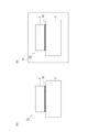
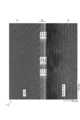
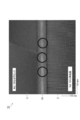
- FIG. 5A is a diagram showing the periphery of the junction portion of the junction element 10 which is an element before the temperature rise step.
- FIG. 5B is an enlarged view showing the inside of the broken line frame of FIG. 5A.
- sapphire is used for the heat sink 2 and Nd: YAG is used for the laser medium 3 (hereinafter, Nd: YAG in the figure is also simply referred to as “YAG”).
- Nd YAG in the figure is also simply referred to as “YAG”).
- the figures of FIGS. 5 (a) and 5 (b) are EDX (Energy dispersive X-ray spectroscopy) data (the same applies to FIGS. 6 to 14 below).
- FIGS. 5A and 5B it can be confirmed that the amorphous layer 16 is interposed between the heat sink 2 and the laser medium 3 in the bonding element 10.
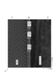
- FIG. 6A is a diagram showing the periphery of the junction portion of the laser element 1 which is the element after the temperature raising step.
- FIG. 6B is an enlarged view showing the inside of the broken line frame of FIG. 6A.
- the laser element 1 of FIGS. 6A and 6B is obtained by heating the bonding element 10 at 1000 ° C. for 3 hours.
- the amorphous layer 16 crystallizes in the temperature raising step, and the crystallized layer 6 is between the heat sink 2 and the laser medium 3. Can be confirmed to be intervening.
- the boundary between the heat sink 2 and the laser medium 3 exists clearly (clearly).
- the amorphous layer 16 has an interface E1 with the heat sink 2.
- the crystallized layer 6 formed by crystallizing the amorphous layer 16 has an interface E2 between the amorphous layer 16 and the heat sink 2.
- the flatness of the interface E2 is higher than the flatness of the interface E1.
- Flatness can be defined, for example, as the magnitude of deviation from a plane. Flatness can be expressed, for example, by the distance between the most protruding and most recessed parts.
- FIG. 7A is a diagram showing the periphery of the junction portion of the junction element 10 which is an element before the temperature rise step.
- FIG. 7B is a graph showing the elements detected within the frame of FIG. 7A.
- the vertical axis is the amount of measurement signal corresponding to the quantity of elements, and the horizontal axis is the scan distance.
- the scanning direction of the graph of FIG. 7 (b) corresponds to the direction from top to bottom in FIG. 7 (a).
- the description of the graph in FIG. 7 (b) is the same for FIGS. 8 (b), 9 (b) and 10 (b).
- the elements constituting the heat sink 2 gradually decrease from the heat sink 2 side to the laser medium 3 side, and the elements constituting the heat sink 2 gradually decrease. It can be confirmed that the elements constituting the laser medium 3 are gradually increasing. Further, it can be confirmed that Fe and Ar are slightly contained as impurities other than the substances constituting the heat sink 2 and the laser medium 3 in the range (25 nm to 40 nm) where the amorphous layer 16 exists.
- FIG. 8A is a diagram showing the periphery of the junction portion of the laser element 1 which is the element after the temperature raising step.
- FIG. 8B is a graph showing the elements detected in the frame of FIG. 8A.
- the laser element 1 of FIGS. 8A and 8B is obtained by heating the bonding element 10 at 1000 ° C. for 3 hours.
- the elements constituting the heat sink 2 gradually decrease from the heat sink 2 side to the laser medium 3 side, and the laser It can be confirmed that the elements constituting the medium 3 are gradually increasing.
- FIG. 9A is a diagram showing the periphery of the junction portion of the laser element 1 which is the element after the temperature raising step.
- FIG. 9B is a graph showing the elements detected in the frame of FIG. 9A.
- the laser element 1 of FIGS. 9A and 9B is obtained by heating the bonding element 10 at 1000 ° C. for 3 hours.
- the result of FIG. 9B is a higher resolution analysis result than the result of FIG. 8B.
- the elements constituting the heat sink 2 gradually decrease from the heat sink 2 side to the laser medium 3 side, and the laser It can be confirmed that the elements constituting the medium 3 are gradually increasing.
- FIG. 10A is a diagram showing the periphery of the joint portion of the laser element 1 which is the element after the temperature raising step.
- FIG. 10B is a graph showing the elements detected within the frame of FIG. 10A.
- the laser element 1 of FIGS. 10A and 10B is obtained by heating the bonding element 10 at 1000 ° C. for 3 hours.
- the results of FIG. 10 (b) show C (carbon), Ar and Fe among the results of FIG. 9 (b).
- the graph of FIG. 10 (b) is superimposed on the position corresponding to the distance of FIG. 10 (b) on FIG. 10 (a).
- FIG. 11A is a diagram showing the periphery of the junction portion of the laser element 1 which is the element after the temperature raising step.
- FIG. 11B is a graph showing the elements detected in the frame of FIG. 11A.
- the laser element 1 of FIGS. 11A and 11B is obtained by heating the bonding element 10 at 1000 ° C. for 3 hours.
- the result of FIG. 11B is a higher resolution analysis result than the result of FIG. 8B.
- the vertical axis is the amount of measurement signal corresponding to the quantity of elements
- the horizontal axis is the scan distance.
- the scanning direction of the graph in FIG. 11B corresponds to the direction from top to bottom in FIG. 11A. As shown in FIG.
- the elements constituting the heat sink 2 in the range where the crystallized layer 6 exists (85 nm to 95 nm), gradually decrease from the heat sink 2 side to the laser medium 3 side, and the laser It can be confirmed that the elements constituting the medium 3 are gradually increasing.
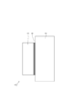
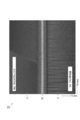
- FIG. 12 is a diagram showing the periphery of the junction portion of the junction element 10 which is an element before the temperature rise step.
- sapphire was used for the heat sink 2 and ceramic YAG was used for the laser medium 3 (the same applies to FIGS. 13 and 14 below).
- the amorphous layer 16 having a thickness of 7 nm or less is interposed between the heat sink 2 and the laser medium 3. Further, here, the unknown layer Q exists near the interface between the heat sink 2 and the laser medium 3.
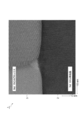
- FIG. 13 is a diagram showing the periphery of the joint portion of the laser element 1 which is an element after the temperature raising step.
- the laser element 1 of FIG. 13 is obtained by heating the bonding element 10 at 100 ° C. for 10 hours.
- crystallization of the amorphous layer 16 is in progress. As shown in FIG. 13, it can be confirmed that the crystallization layer 6 is interposed between the heat sink 2 and the laser medium 3.
- the crystallization layer 6 is formed in a layered state including a plurality of layers.
- the crystallization layer 6 includes a 2.6 nm layer, a 1.7 nm layer, and a 2.2 nm layer from the heat sink 2 side toward the laser medium 3 side at a certain position.
- the crystallization layer 6 includes a 2.6 nm layer, a 2.0 nm layer, and a 1.7 nm layer from the heat sink 2 side toward the laser medium 3 side at other points.
- the crystallization layer 6 includes a 2.6 nm layer, a 1.7 nm layer, and a 2.0 nm layer from the heat sink 2 side toward the laser medium 3 side at still other points.
- the coefficient of progress of crystallization is 0.5 nm / h.
- FIG. 14 is a diagram showing the periphery of the joint portion of the laser element 1 which is an element after the temperature raising step.
- the laser element 1 of FIG. 14 is obtained by heating the bonding element 10 at 100 ° C. for 24 hours.
- the crystallization of the amorphous layer 16 is more advanced. As shown in FIG. 14, it can be confirmed that the crystallization layer 6 is interposed between the heat sink 2 and the laser medium 3.
- the crystallization layer 6 includes a 1.8 nm layer and a 3.4 nm layer from the heat sink 2 side toward the laser medium 3 side at a certain location.
- the crystallization layer 6 includes a 3.1 nm layer and a 1.7 nm layer from the heat sink 2 side toward the laser medium 3 side at other points.
- the crystallization layer 6 includes a 3.3 nm layer and a 1.7 nm layer from the heat sink 2 side toward the laser medium 3 side at still other points.
- the coefficient of progress of crystallization is 0.5 nm / h.
- the amorphous layer 16 is epitaxially grown by raising the temperature of the bonding element 10, the amorphous layer 16 is crystallized, and the material state (bonding state) of the laser element 1 is stabilized.
- the bonding characteristics can be improved without deteriorating the characteristics of the bonding portion.
- the bonding step at least one of the surface on the bonding side of the heat sink 2 and the surface on the bonding side of the laser medium 3 is irradiated with an ion beam or a high-speed atomic beam in a substantially vacuum environment.
- the bonding element 10 can be obtained by bringing the surface of the heat sink 2 on the bonding side into contact with the surface of the laser medium 3 on the bonding side.
- the temperature raising step there is a concern that stress is generated at the joint portion due to the difference in the coefficient of linear expansion, causing damage such as peeling to the laser element 1.
- the amorphous layer 16 contains the beam source element constituting the ion beam or the high-speed atomic beam and / or impurities of the beam housing material
- the temperature required for epitaxial growth at the time of temperature rise is set to the heat sink 2. And it is found that the temperature can be lowered to a predetermined temperature much lower than the melting point of the laser medium 3.
- the amorphous layer 16 contains the beam source element and / or the beam housing material, and the temperature of the temperature rise is lowered to a predetermined temperature lower than the melting points of the heat sink 2 and the laser medium 3. ing. Therefore, it is possible to suppress the damage of the laser element 1. Since the crystallized layer 6 does not require a high temperature for the solid-phase reaction, ideal crystal growth with less distortion is possible.
- the heat sink 2 is formed of diamond, silicon carbide, sapphire, garnet containing YAG, vanadate, laser material to which rare earth ion or transition metal is added, optical switch material, nonlinear optical material, functional optical material, Or it is ceramics.
- the laser medium 3 is a laser material to which diamond, silicon carbide, sapphire, garnet containing YAG, vanadate, rare earth ion or transition metal is added, an optical switch material, a nonlinear optical material, a functional optical material, or a ceramic.
- the predetermined temperature which is the temperature at which the temperature is raised (epi growth temperature), is 100 ° C. or higher and 1100 ° C. or lower. With respect to the laser element 1 provided with such a heat sink 2 and a laser medium 3, it is possible to stabilize the material state of the laser element 1 by raising the temperature and suppress damage to the laser element 1 at the time of raising the temperature. ..
- the ceramics include those having a Faraday effect such as TGG (terbium gallium garnet), TAG (terbium aluminum garnet), and TSAG (terbium scandium aluminum garnet) ceramics. Ceramics are vulnerable to damage due to grain boundaries at the end faces, and must be joined and used for protection. Since ceramics cannot be made to a thickness of about 10 mm, joining is indispensable when using a thick material. When ceramics are bonded, it is desirable to stabilize them by a temperature raising step (annealing treatment) because the bonding boundary material is unstable.
- annealing treatment a temperature raising step
- a crystallized layer 6 is interposed between the heat sink 2 and the laser medium 3 instead of the amorphous layer 16, and the crystallized layer 6 moves from the heat sink 2 side to the laser medium 3 side.
- the elements constituting the heat sink 2 gradually decrease, and the elements constituting the laser medium 3 gradually increase. According to such a configuration, it is possible to stabilize the material state of the laser element 1.
- the amorphous layer 16 the element changes relatively slowly, but in the crystallized layer 6, the change of the element becomes steep.
- FIG. 15 is a cross-sectional view showing the laser element 101 according to the modified example.
- the optical coating layer 12 is formed on the surface of the heat sink 2 by applying an optical coating to the surface of the heat sink 2.
- the optical coating is not particularly limited, and various known optical coatings can be adopted.
- the optical coating layer 12 is a part of the heat sink 2 and constitutes the surface side of the heat sink 2. That is, the heat sink 2 has an optical coating layer 12 on the joint side portion thereof.
- the heat sink 2 is not limited to the heat sink 2, and other laser materials may be used, an optical switch such as Cr: YAG may be used, or a crystal, LN, LBO, KTP, GaAs, It may be a nonlinear optical crystal such as GaP, ZnSe, ZnS.
- a layer that becomes transparent by temperature rise treatment that is, a semiconductor material such as Si, Ga, Zn, or Si, Al, Ti, Hf, Mg, Zr, Ta, Nb is deposited. Sometimes it makes me.
- the final layer of the optical coating layer 12 has a layer that becomes transparent by the temperature raising treatment. After joining the heat sink 2 and the laser medium 3, the layer that becomes transparent due to the temperature rise treatment becomes an oxide or compound by heat treatment in an oxygen atmosphere or the like as an appropriate environment, and is sufficiently transparent in the desired laser wavelength range. To serve its function.
- an optical coating is applied to the surface of the heat sink 2, and the heat sink 2 and the laser medium 3 are bonded by surface active bonding to form a bonding element.
- the bonded element is heat-treated to raise the temperature of the bonded element to a predetermined temperature.
- the bonding element is annealed, and the amorphous layer of the bonding element is epitaxially grown and crystallized, resulting in the laser element 101 shown in FIG.
- the predetermined temperature for raising the temperature is lower than the melting points of the heat sink 2 and the laser medium 3.
- the predetermined temperature for raising the temperature is 100 ° C. or higher and 600 ° C. or lower.
- the heat sink 2 has an optical coating layer 12 on the joint side portion thereof, and the predetermined temperature for raising the temperature is 100 ° C. or higher and 600 ° C. or lower. .. Deterioration of the optical coating layer 12 is observed when the temperature is raised to about 800 ° C. or higher. Therefore, in the method for manufacturing the laser element 101 according to the modified example, damage to the optical coating layer 12 can be suppressed. Recrystallization, that is, epi-growth, is possible by raising the temperature at a sufficiently low temperature so that the optical coating layer 12 is not damaged.
- the laser medium 3 may have an optical coating layer on the junction side portion thereof, or both the heat sink 2 and the laser medium 3 may have an optical coating layer on the junction side portion thereof.
- the predetermined temperature for raising the temperature may be 800 ° C. or lower, 200 ° C. to 300 ° C., 100 ° C., or higher than the joining temperature.
- the heat sink 2 is made of SiC or diamond, the optical coating layer 12 is particularly effective because the refractive indexes are significantly different.
- the junction temperature is preferably the temperature at which the substance is used.
- the final layer a layer that becomes transparent by temperature rise treatment, that is, a semiconductor material such as Si, Ga, Zn, or Si, Al, Ti, Hf, Mg, Zr, Ta, Nb is deposited. Sometimes it makes me.
- the final layer of the optical coating layer has a layer that becomes transparent by the temperature raising treatment.
- the layer that becomes transparent due to the temperature rise treatment becomes an oxide or compound by heat treatment in an oxygen atmosphere or the like as an appropriate environment, and is sufficiently transparent in the desired laser wavelength range. To serve its function.
- the following effects are also achieved. That is, it is possible to join not only the same kind of materials but also different kinds of materials that are generally difficult to join. Any material such as metal, glass and film can be bonded. It does not take heat and can suppress deformation due to heat. No adhesive is required. The joint strength can be controlled. Not only strong bonding but also temporary bonding assuming peeling can be supported. Since the joining time is short, the joining can be completed in seconds in principle. There is no deviation after joining, and high alignment accuracy can be achieved.
- Nd YAG
- Cr YAG as the passive Q-switch medium
- Nd: YAG is usually shortened in order to shorten the resonator.
- a highly reflective coating regarding the excitation wavelength is applied to the surface opposite to the excitation side (the boundary surface of Cr: YAG) to halve L 0 .
- the coating layer interferes and cannot be joined.
- the bonded insert made of ceramic YAG is generally long, and the obtained pulse width is also long. That is, only laser light sources with low performance and weak competitiveness can be made.
- a microchip capable of generating a short pulse width can be expected from the ceramic YAG. Since it is possible to join a large area, the ceramic YAG composite can be mass-produced and the cost can be reduced by molding a large area at once and cutting it into small chips. In particular, in the present embodiment, it is possible to further increase the area and join with a higher joining strength, and the mass production effect and cost reduction due to the larger size are remarkable. It is possible to manufacture optical elements with high performance and high reliability.
- each of the above numerical values may include errors in design, measurement, manufacturing, and the like.
- the laser element 1 according to one embodiment of the present invention can be applied to various laser components and thus to a laser device, and the laser device can be used in various devices such as a measuring device, a processing device, a diagnostic device, and a medical device. ..
- the entire amorphous layer 16 is crystallized by raising the temperature of the bonding element 10 in the temperature raising step, but the entire amorphous layer 16 is not limited to crystallizing. At least a part of the amorphous layer 16 may be crystallized.
- the amorphous layer 16 may be a mixed crystal system of Si and YAG, or a mixed crystal system of Si and sapphire. These melting points are very high, about 2000 ° C., but the predetermined temperature, which is the epi growth temperature, is much lower than that.
- One embodiment of the present invention may include a spatial modulation element that controls the spatial mode of the laser beam.
- the spatial modulation element may or may not be bonded to the heat sink 2 and the laser medium 3. This makes it possible to configure a high-luminance and high-output microamplifier.
- the first element portion and the second element portion are surface-actively bonded, but in the surface-active bonding, it is not necessary to create a substantially vacuum environment when the heat sink 2 and the laser medium 3 are brought into contact with each other.
- the second element portion is gold (Au), copper (Cu), copper tungsten (CuW), aluminum (Al), iron (Fe), titanium (Ti), or any of these. It may be a metal containing at least any alloy.
- the optical element according to one embodiment of the present invention can be applied to any optical element as long as it is an optical element that transmits, reciprocates, or reflects laser light.
- the optical element according to one embodiment of the present invention is not limited to an oscillator, but also includes an amplifier, a functional optical material (Q-switch element such as Cr: YAG), a nonlinear optical material, and a wavelength conversion element such as QPM-crystal.
- the material to be bonded may be not only a combination of a laser medium and a heat sink, but also an optical switch such as a saturable absorber, a nonlinear optical material for wavelength conversion, and the like.
- the transmittance of transparency does not necessarily have to be 95% or more.
- the configuration bonded via the crystallization layer is not particularly limited to those described above, and may be, for example, the optical elements of the following configuration examples 1 to 4.
- the laser medium is, for example, RE: single crystal / ceramics (YAG, YSGG, YLF, YVO 4 , SFAP, etc.), RE: glass.
- the Q-switch element is, for example, Cr: YAG.
- the transparent heat sink is, for example, YAG, sapphire, SiC, or diamond.
- (Configuration Example 2) An optical element including a transparent heat sink, a laser medium laminated on the heat sink, and a crystallization layer between them. (Configuration Example 3) Between the transparent heat sink, the laser medium laminated on the transparent heat sink, the Q-switch element laminated on the laser medium, the crystallization layer between the transparent heat sink and the laser medium, and between the laser medium and the Q-switch. An optical element including a crystallized layer. (Configuration Example 4) Between the transparent heat sink, the laser medium laminated on the transparent heat sink, the Q-switch element laminated on the laser medium, the transparent heat sink laminated on the Q-switch, the transparent heat sink, and the laser medium adjacent thereto. An optical element including a crystallization layer, a crystallization layer between a laser medium and a Q-switch, and a crystallization layer between a Q-switch element and a transparent heat sink adjacent thereto.
- a known coating layer may be appropriately provided on each member (first element portion and second element portion) constituting the optical element. Since the refractive indexes of Nd: YAG and Cr: YAG are substantially the same, direct bonding via a crystallization layer is possible without requiring an AR (Anti Reflection) coating as a coating layer. However, in order to improve the excitation efficiency, an HR (High Reflection) coating having a target wavelength of 808 nm or 885 nm and an AR coating having a target wavelength of 1064 nm may be provided as the coating layer.
- an HR High Reflection
- one embodiment of the present invention includes variations such as a configuration in which a coating (optical coating) is applied and bonded to the coating (optical coating) via a crystallization layer.
- the transparent first element portion and the second element portion include an optical switch element such as a transparent Q-switch element when the switch is ON.
- the combination of element parts to be joined is an optical gain medium, Q switch element, heat sink (YAG, sapphire, SiC, diamond, opaque material such as Al, Cu, CuW), nonlinear optical element (nonlinear wavelength conversion (SHG)). , Raman element, etc.), nonlinear optical switch, etc.), wave plate, polarizer, beam splitter, beam coupling element, etc., which may be an appropriate combination.
- the Q-switch element includes not only conventional AO (Acousto Optic) and EO (Electro Optic) but also MO (Magneto Optic).
- a wave plate or a polarizer may be arranged inside the resonator for bonding.
- a nonlinear optical wavelength conversion element may be included, or a beam splitter or a beam coupling element may be included.
- the excitation light may be introduced from the heat sink. Joining a transparent heat sink is also effective in preventing parasitic oscillation.
- metal is used as the heat sink.
- the metal is Al or an alloy thereof, and further, when only the outermost surface portion of the heat sink is Al or the like, the laser medium is coated with HR for the emitted laser light, and then the heat sink is joined by some method.
- an alumina layer is sputtered or vapor-deposited on the outside of the HR coat, and then both are sandwiched between anvils or the like, and a giant pulse laser beam having a different wavelength transmitted through the HR coat is irradiated therein to form an element forming a heat sink. It is also effective to mix the elements constituting the laser medium and the elements constituting the laser medium non-thermally at the crystal level to bond them.
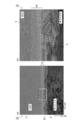
- FIG. 16 is a diagram showing the periphery of the junction portion of the junction element 10 which is an element before the temperature rise step.
- Nd YAG ceramics were used for the heat sink 2
- Nd YAG single crystal was used for the laser medium 3 (the same applies to FIGS. 17 to 22 below).
- the figure of FIG. 16 is EDX data (the same applies to FIGS. 17 and 22 below).
- the amorphous layer 16 is interposed in the bonding element 10 before the temperature raising step (before the annealing treatment).
- the amorphous layer 16 has a thickness of 10 to 15 nm.
- FIG. 17 is a diagram showing the periphery of the joint portion of the laser element 1 which is an element after the temperature raising step. As shown in FIG. 17, it can be confirmed that the amorphous layer 16 (see FIG. 16) has disappeared in the laser element 1 after the temperature raising step (after the annealing treatment). Nd: The expansion of the region of the YAG single crystal (epitaxial growth) can be verified.
- FIG. 18 is a diagram showing the periphery of the joint portion of the laser element 1 which is an element after the temperature raising step.
- FIG. 19 is a graph showing the elements detected at the positions shown in FIG. 18 in the scanning direction.
- FIG. 20 is a diagram showing the periphery of the junction portion of the junction element 10 which is an element before the temperature rise step.
- FIG. 21 is a graph showing the elements detected at the positions shown in FIG. 20 in the scanning direction.
- FIGS. 18 and 20 are bright-field images which are STEM images created by detecting electrons that are transmitted without being scattered and electrons that are scattered at a small angle among the transmitted electrons. ..
- the vertical axis represents the amount of measurement signal corresponding to the quantity of elements
- the horizontal axis represents the scan distance.
- the scanning direction of the graph in FIG. 19 corresponds to the direction from top to bottom in FIG.
- the scanning direction of the graph in FIG. 21 corresponds to the direction from top to bottom in FIG.
- FIGS. 18 to 21 it is confirmed that the elements constituting the heat sink 2 gradually decrease and the elements constituting the laser medium 3 gradually increase, for example, from the heat sink 2 side to the laser medium 3 side. it can.
- FIG. 22 is a diagram showing the periphery of the bonding portion of the bonding element 10 after the EB irradiation, which is the element before the temperature rising step.
- the instability of the amorphous layer 16 at the junction interface between Nd: YAG ceramics and Nd: YAG single crystal is remarkable, and as shown in the circle frame in FIG. 22, after EB (Electron Beam) irradiation during analysis, It can be confirmed that voids are generated in the amorphous layer 16. Before EB irradiation, the amorphous layer 16 was not damaged (see FIG. 16). When the amorphous layer is crystallized by the temperature raising step (annealing treatment), such damage is not observed.
- the ceramic region which is a polycrystalline material including the bonding interface, is single-crystallized, and the ceramic-derived characteristic deterioration, such as orientation and electrons at the grain interface, is achieved. And phonon scattering are suppressed.
- a method of surface-actively bonding an arbitrary ceramic material and a single crystal and then single-crystallizing by raising the temperature is effective for improving the characteristics of the material.
- one aspect of the present invention is a ceramic region which is a polycrystal including a bonding interface by heating a single crystal to ceramics after surface active bonding. Is characterized by being single crystallized by a solid phase method below the melting point.
- one aspect of the present invention is an optical element that transmits, reciprocates, or reflects laser light, the first element portion that is transparent to the laser light, and the first element portion.
- a crystallization layer interposed between the second element portion and the first element portion and the second element portion and formed by crystallization is provided, and the crystallization layer is from the first element portion side to the second element portion side.
- the elements constituting the first element portion are continuously exchanged with the elements constituting the second element portion.
- one aspect of the present invention is an optical element that transmits, reciprocates, or reflects laser light, and is a first element portion that is transparent to the laser light.
- a crystallized layer interposed between the second element portion and the first element portion and the second element portion is provided, and at least one of the first element portion and the second element portion is joined.
- the elements constituting the first element portion or the second element portion continuously in the 10 nm region. It is replaced with the elements that make up the optical coating layer.
- At least one of the first element portion and the second element portion has an optical coating layer on the junction side portion thereof and crystallizes.
- the chemical layer contains at least one of Ar, Ne, Xe, He, Fe, Ni and Cr.
Landscapes
- Physics & Mathematics (AREA)
- Electromagnetism (AREA)
- Engineering & Computer Science (AREA)
- Chemical & Material Sciences (AREA)
- Optics & Photonics (AREA)
- Plasma & Fusion (AREA)
- Ceramic Engineering (AREA)
- Materials Engineering (AREA)
- Organic Chemistry (AREA)
- Crystallography & Structural Chemistry (AREA)
- Life Sciences & Earth Sciences (AREA)
- Chemical Kinetics & Catalysis (AREA)
- General Chemical & Material Sciences (AREA)
- Geochemistry & Mineralogy (AREA)
- Structural Engineering (AREA)
- General Physics & Mathematics (AREA)
- Lasers (AREA)
- Optical Modulation, Optical Deflection, Nonlinear Optics, Optical Demodulation, Optical Logic Elements (AREA)
- Manufacturing & Machinery (AREA)
Abstract
光学素子の製造方法は、レーザ光が透過、往復又は反射する光学素子を製造する方法であって、レーザ光に対して透明な第1素子部及び第2素子部が非晶質層を介して表面活性接合されてなる接合素子を得る第1ステップと、第1ステップの後、接合素子を昇温することで、非晶質層の少なくとも一部を結晶化する第2ステップと、を備える。第2ステップにおいては、第1素子部及び第2素子部の融点よりも低い所定温度まで接合素子を昇温する。
Description
本発明の一側面は、レーザ光が透過、往復又は反射する光学素子の製造方法、及びその光学素子に関する。
従来の光学素子の製造方法として、出射するレーザ光に対して透明な第1素子部及び第2素子部を表面活性により直接接合する方法が知られている(例えば、特許文献1参照)。このような光学素子の製造方法では、非晶質層を第1素子部と第2素子部との間に介在させることで、第1素子部と第2素子部との良好な接合が可能とされている。
上記従来技術では、例えば第1素子部と第2素子部とが異種材料であっても、前述のように非晶質層を介することで、両者の接合が可能である。しかし、非晶質層は準安定状態であることから、光学素子の物質状態(接合状態)が不安定となり、例えば光学素子の光学耐性等の強度が不十分となる可能性がある。
本発明の一側面は、上記実情に鑑みてなされたものであり、物質状態を安定化させることが可能な光学素子の製造方法及び光学素子を提供することを課題とする。
本発明の一側面に係る光学素子の製造方法は、レーザ光が透過、往復又は反射する光学素子を製造する方法であって、レーザ光に対して透明な第1素子部及び第2素子部が非晶質層を介して表面活性接合されてなる接合素子を得る第1ステップと、第1ステップの後、接合素子を昇温することで、非晶質層の少なくとも一部を結晶化する第2ステップと、を備え、第2ステップにおいては、第1素子部及び第2素子部の融点よりも低い所定温度まで接合素子を昇温する。
本発明の一側面に係る光学素子の製造方法では、接合素子を昇温することで非晶質層をエピタキシャル成長させ、非晶質層の少なくとも一部を結晶化し、光学素子の物質状態(接合状態)を安定化させることができる。
本発明の一側面に係る光学素子の製造方法は、第1ステップでは、略真空環境下において、第1素子部の接合側の表面及び第2素子部の接合側の表面の少なくとも何れかにイオンビーム又は高速原子ビームを照射した後、第1素子部の表面と第2素子部の表面とを接触させることで、接合素子を得てもよい。
本発明の一側面に係る光学素子の製造方法では、第1ステップにおいて、非晶質層は、第1素子部及び第2素子部を構成する物質以外の不純物として、イオンビーム又は高速原子ビームを構成するビーム源元素、及び、イオンビーム又は高速原子ビームのビーム筐体を構成するビーム筐体材料の少なくとも何れかを含んでいてもよい。ここで、接合素子を昇温する際、線膨張係数の違いから接合部分に応力が発生し、光学素子に剥離等の損傷が生じることが懸念される。この点、非晶質層に不純物としてビーム源元素及び/又はビーム筐体材料が含まれると、昇温の際におけるエピタキシャル成長に必要な温度を、第1素子部及び第2素子部の融点よりも低い所定温度まで下げ得ることが見出される。そこで、本発明の一側面に係る光学素子の製造方法では、非晶質層がビーム源元素及び/又はビーム筐体材料を含み、昇温の温度が第1素子部及び第2素子部の融点よりも低い所定温度まで下げられている。これにより、光学素子の当該損傷を抑制することができる。
本発明の一側面に係る光学素子の製造方法では、第1素子部は、ダイアモンド、シリコンカーバイド、サファイア、YAGを含むガーネット、バナデート、セクスオキサイド、フロライド、アパタイト、タングステート、シリケート、リン酸系の材料、希土類イオンもしくは遷移金属を添加したレーザ材料、光スイッチ材料、非線形光学材料、又は、機能性光学材料であり、第2素子部は、ダイアモンド、シリコンカーバイド、サファイア、YAGを含むガーネット、バナデート、セクスオキサイド、フロライド、アパタイト、タングステート、シリケート、リン酸系の材料、希土類イオンもしくは遷移金属を添加したレーザ材料、光スイッチ材料、非線形光学材料、又は、機能性光学材料であり、第2ステップの所定温度は、100℃以上で且つ非晶質層を構成する物質の融点より低い温度であってもよい。この場合、このような第1素子部及び第2素子部を備えた光学素子について、昇温により光学素子の物質状態を安定化させることが可能となる。
なお、ガーネットにはYAG,YSAG,YGAG,GGG,GSGG,LuAG,YALOなどの酸化物、バナデートは、例えばYVO4もしくはGdVO4,LuVO4等のVO4化合物、セクスオキサイドはY2O3,Sr2O3,Lu2O3,フロライドにはYLF,SrF2,CaF2などのフッ化物、アパタイトにはFAP,SFAP,VAP,SVAPなどリン酸系カルシウム化合物、タングステートとはKYW,KGWなどのWO4化合物である。機能性光学材料は、例えば水晶、LBO、LiNbO3、KTiPO4、ZGP、GaAsもしくはGaP,ZnSe,ZnSなど非線形感受率や電気光学効果、磁気光学効果を有する材料である。セラミックスは、例えば、TGG(テルビウム・ガリウム・ガーネット)、TAG(テルビウム・アルミニウム・ガーネット)、TSAG(テルビウム・スカンジウム・アルミニウム・ガーネット)セラミックス等のファラデー効果を有するものが挙げられる。
なお、ガーネットにはYAG,YSAG,YGAG,GGG,GSGG,LuAG,YALOなどの酸化物、バナデートは、例えばYVO4もしくはGdVO4,LuVO4等のVO4化合物、セクスオキサイドはY2O3,Sr2O3,Lu2O3,フロライドにはYLF,SrF2,CaF2などのフッ化物、アパタイトにはFAP,SFAP,VAP,SVAPなどリン酸系カルシウム化合物、タングステートとはKYW,KGWなどのWO4化合物である。機能性光学材料は、例えば水晶、LBO、LiNbO3、KTiPO4、ZGP、GaAsもしくはGaP,ZnSe,ZnSなど非線形感受率や電気光学効果、磁気光学効果を有する材料である。セラミックスは、例えば、TGG(テルビウム・ガリウム・ガーネット)、TAG(テルビウム・アルミニウム・ガーネット)、TSAG(テルビウム・スカンジウム・アルミニウム・ガーネット)セラミックス等のファラデー効果を有するものが挙げられる。
本発明の一側面に係る光学素子の製造方法では、第1素子部及び第2素子部の状態は、単結晶、アモルファス(ガラスを含む)、又はセラミックスであってもよい。
本発明の一側面に係る光学素子の製造方法では、第1素子部及び第2素子部の少なくとも一方は、その接合側部分に光学コーティング層を有し、所定温度は、100℃以上600℃以下であってもよい。これにより、光学コーティング層の損傷についても抑制することが可能となる。
本発明の一側面に係る光学素子の製造方法では、第2ステップで非晶質層を結晶化してなる結晶化層が有する界面の平面度は、非晶質層が有する界面の平面度よりも高くてもよい。これにより、透過、往復又は反射するレーザ光に対して界面が与える悪影響の可能性を抑制することが可能となる。
本発明の一側面に係る光学素子は、レーザ光が透過、往復又は反射する光学素子であって、レーザ光に対して透明な第1素子部及び第2素子部と、第1素子部と第2素子部との間に介在され、結晶化してなる結晶化層と、を備え、結晶化層は、第1素子部側から第2素子部側に行くに従って、10nm領域で第1素子部を構成する元素が連続的に第2素子部を構成する元素に交換している。
本発明の一側面に係る光学素子は、レーザ光が透過、往復又は反射する光学素子であって、レーザ光に対して透明な第1素子部及び第2素子部と、第1素子部と第2素子部との間に介在され、結晶化してなる結晶化層と、を備え、結晶化層は、Ar、Ne、Xe、He、Fe、Ni及びCrの少なくとも何れかを含んでいる。
この光学素子では、第1素子部及び第2素子部との間には、非晶質層ではなく、結晶化層が介在されている。結晶化層は、Ar、Ne、Xe、He、Fe、Ni及びCrの少なくとも何れかを含んでいる。そのため、再結晶化に有利となる(微量の不純物混入により低温での昇温処理での再結晶化が容易なだけで無く、通常温度での昇温処理であれば短時間での再結晶化が可能となる)。
本発明の一側面に係る光学素子は、レーザ光が透過、往復又は反射する光学素子であって、レーザ光に対して透明な第1素子部及び第2素子部と、第1素子部と第2素子部との間に介在され、結晶化してなる結晶化層と、を備え、第1素子部及び第2素子部の少なくとも一方は、その接合側部分に光学コーティング層を有し、光学コーティング層に接する第1素子部又は第2素子部の結晶化層において、10nm領域で第1素子部又は第2素子部を構成する元素が連続的に光学コーティング層を構成する元素に交換している。
本発明の一側面に係る光学素子は、第1素子部及び第2素子部の少なくとも一方は、その接合側部分に光学コーティング層を有し、結晶化層は、Ar、Ne、Xe、He、Fe、Ni及びCrの少なくとも何れかを含んでいてもよい。
本発明の一側面によれば、物質状態を安定化させることが可能な光学素子の製造方法及び光学素子を提供することが可能となる。
以下、図面を参照しつつ実施形態について詳細に説明する。以下の説明において同一又は相当要素には同一符号を付し、重複する説明を省略する。
図1は、小型集積レーザ装置100を示す概略斜視図である。図1に示される小型集積レーザ装置100は、レーザ光Lを出射するレーザ光源であって、ファイバレーザやディスクレーザに比べて小型簡便で高出力のパワーレーザを構成する。小型集積レーザ装置100は、実施形態に係るレーザ素子1を備える。なお、以下においては、便宜上、レーザ光Lの出射方向(進行方向)を「Z方向」として説明する。図2以降に示す断面は、XY断面であり、面内横軸を「X方向」とし、面内縦軸を「Y方向」とする。図面の寸法比率は図示の比率に限られるものではない。
まず、レーザ素子1の構成について説明する。
レーザ素子1は、DFC構造を有する光学素子である。レーザ素子1は、複数のヒートシンク2と、複数のレーザ媒質3と、第1コーティング層4aと、第2コーティング層5と、第3コーティング層4bと、を備える。レーザ素子1は、高出力マイクロレーザを構成可能なものである。一例として、レーザ素子1では、波長808nmの連続発振のダイオード光が励起光Iとして、Z方向における一端側(図示左側)からZ方向に沿って入力されると、波長1064nmのレーザ光Lが、可飽和吸収体からなるQスイッチ素子8を介してZ方向における他端側(図示右側)から出射される。なお、レーザ素子1は、Qスイッチ素子8を備えない場合、CW(Continuous Wave)レーザを構成することも可能である。
ヒートシンク2及びレーザ媒質3は、Z方向を厚さ方向とする矩形板状を呈する。例えばヒートシンク2は、厚さが1mm、縦寸法が10mm、横寸法が10mmの平板状を呈する。例えばレーザ媒質3は、厚さが1mm、縦寸法が8mm、横寸法が8mmの平板状を呈する。ヒートシンク2及びレーザ媒質3は、円形板状を呈していてもよい。ヒートシンク2とレーザ媒質3とは、Z方向に沿って交互に並ぶように配置されている。つまり、隣接する一対のヒートシンク2の間に、レーザ媒質3が位置する。ヒートシンク2とレーザ媒質3とは、接着剤を介さずに接合(直接接合)されている。Z方向において最も一端側に配されたレーザ媒質3から最も他端側に配されたレーザ媒質3までの部分は、共振器として機能する。
ヒートシンク2は、レーザ媒質3に比べて熱伝導率が同程度か又は高い物質である。ヒートシンク2は、レーザ媒質3の熱を放熱する機能を有する。ヒートシンク2は、第1素子部を構成する。ヒートシンク2は、ダイアモンド、シリコンカーバイド、サファイア、YAGを含むガーネット、バナデート、セクスオキサイド、フロライド、アパタイト、タングステート、シリケート、リン酸系の材料、希土類イオンもしくは遷移金属を添加したレーザ材料、光スイッチ材料、非線形光学材料、又は、機能性光学材料である。なお、バナデートは、例えばYVO4もしくはLuVO4等である。機能性光学材料は、例えばLBO、LiNbO3、KTiPO4、ZGP、GaAsもしくはGaPである。後述もしているが、ヒートシンク2は第1素子部の一例であり、第1素子部はヒートシンク2に限定されない。第1素子部の状態は、単結晶、アモルファス(ガラスを含む)、又はセラミックスであればよい。
レーザ媒質3は、励起状態において増幅が損失を上回る反転分布を形成し、誘導放出を利用して光を増幅させる物質である。レーザ媒質3は、利得媒質とも称する。レーザ媒質3は、第2素子部を構成する。レーザ媒質3は、ダイアモンド、シリコンカーバイド、サファイア、YAGを含むガーネット、バナデート、セクスオキサイド、フロライド、アパタイト、タングステート、シリケート、リン酸系の材料、希土類イオンもしくは遷移金属を添加したレーザ材料、光スイッチ材料、非線形光学材料、又は、機能性光学材料である。半導体は、例えばZnSもしくはZnSe等である。後述もしているが、レーザ媒質3は第2素子部の一例であり、第2素子部はレーザ媒質3に限定されない。第2素子部の状態は、単結晶、アモルファス(ガラスを含む)、又はセラミックスであればよい。
ヒートシンク2及びレーザ媒質3は、出射するレーザ光Lに対して透明である。レーザ光Lに対して透明(以下、単に「透明」ともいう)とは、レーザ光Lが透過することを意味し、具体的には、レーザ光Lが強度を維持して通過することを意味する。例えば透明とは、ここでは、レーザ光Lに対する透過率(Fresnel損失分を差し引いた正味の透過率)が95%以上をいい、具体的には、97%以上であることをいう。このことは、以下の透明において同様である。
第1コーティング層4は、Z方向における一端側のヒートシンク2において、一端側の表面(大気と接する面)に形成された誘電多層膜である。第1コーティング層4は、励起光Iに対しては無反射で、且つ、レーザ光Lに対しては高反射の反射特性を有する。第1コーティング層4によれば、一端側のヒートシンク2と大気との間における屈折率の変動を抑えることができる。
第2コーティング層5は、Z方向における他端側のヒートシンク2において、他端側の表面(大気と接する面)に形成された誘電多層膜である。第2コーティング層5は、励起光Iに対しては高反射で、且つ、レーザ光Lに対しては一部反射の反射特性を有する。第2コーティング層5によれば、他端側のヒートシンク2と大気との間における屈折率の変動を抑えることができる。ちなみに、第1コーティング層4及び第2コーティング層5の少なくとも何れかに代えてもしくは加えて、他の種々のコーティング層をヒートシンク2及びレーザ媒質3に適宜設けてもよい。これにより、ヒートシンク2及びレーザ媒質3の各界面での反射特性を所望に調整することができる。
レーザ素子1は、図4に示されるように、結晶化層6を備える、結晶化層6は、ヒートシンク2及びレーザ媒質3との間に介在されている緩衝層である。レーザ素子1は、結晶化してなる層、すなわち、結晶状態の層である。結晶とは、空間的に周期的な原子配列を持った固体物質である。結晶とは、原子や分子が空間的に繰り返しパターンを持って配列している物質である。具体的には、結晶とは、離散的な空間並進対称性を有する物質である。ここでの結晶は、準結晶を含む。結晶化層6は、ヒートシンク2側からレーザ媒質3側に行くに従って、ヒートシンク2を構成する元素が漸減する(次第に減る)と共に、レーザ媒質3を構成する元素が漸増する(次第に増える)層である(図8~図11参照)。結晶化層6は、ヒートシンク2及びレーザ媒質3と一体化されている。結晶化層6は、レーザ光Lに対して透明であり、レーザ光Lを透過させる。
なお、ヒートシンクの材料及びレーザ媒質の材料としては、下表1の組合せが挙げられる。ただし、REは、Ce,Pr,Nd,Sm,Eu,Tb,Dy,Ho,Er,Tm,Yb等の添加希土類元素である。TMは、Mg,Ca,Mn,Fe,Co,Ni,Cu,Zn,Cr,Ti,Te,Nb,V等の添加遷移金属元素である。後述するように、ヒートシンク及びレーザ媒質に光学コーティングを施してから接合する場合もある。

次に、レーザ素子1の製造方法について説明する。
レーザ素子1の製造方法では、概略として、まず、複数のヒートシンク2及び複数のレーザ媒質3を用意する。第1コーティング層4及び第2コーティング層5をヒートシンク2に適宜成膜する。当該成膜には、公知の種々の成膜手法を採用できる。続いて、接合ステップ(第1ステップ)として、ヒートシンク2及びレーザ媒質3を交互に並ぶように配置しつつ、ヒートシンク2及びレーザ媒質3を非晶質層16を介して直接接合し、接合素子を得る。そして、昇温ステップ(第2ステップ)として、当該接合素子を昇温することで、その非晶質層16の少なくとも一部を結晶化する。
以下、接合ステップ及び昇温ステップを詳説する。図2(a)、図2(b)及び図3(a)は、接合ステップを説明するための各図である。図3(b)及び図4は、昇温ステップを説明するための各図である。以下では、説明の便宜上、1つのヒートシンク2と1つのレーザ媒質3との接合を例示する。また、ヒートシンク2及びレーザ媒質3を図1のA-A線に沿う断面で示すが、当該断面にハッチングは施していない(その他の断面図において同様)。
図2(a)に示されるように、ヒートシンク2及びレーザ媒質3をチャンバー11内に配置し、チャンバー11内を略真空環境とする。ヒートシンク2とレーザ媒質3とを表面活性接合により接合する。表面活性接合は、真空中で接合する材料の接合面の酸化膜又は表面付着物を、イオンビーム照射又はFAB(高速原子ビーム)照射によって除去し、平坦で構成原子の露出した接合面同士を接合するという手法である。表面活性接合は、分子間結合を利用した直接接合である。表面活性接合は、他の接合手法と比較して接合温度を大幅に下げることができる。
具体的には、略真空環境下において、ヒートシンク2の接合側の表面、及び、レーザ媒質3の接合側の表面に、アルゴン(Ar)等のイオンビーム又はFAB(高速原子ビーム)を照射する。これにより、当該表面に吸着していた酸素等を除去し、ダングリングボンドを含む新生面を形成する。当該略真空環境は、例えばバックグラウンド圧力が1×10⁻⁶Pa以上、大気圧未満の真空又は減圧雰囲気である。
イオンビーム又はFABとしては、アルゴンの他に、ネオン(Ne)、クリプトン(Kr)、キセノン(Xe)、ヘリウム(He)等の希ガス又は不活性ガスを採用することができる。希ガスは、化学反応を起こしにくいので、被照射面の化学的性質を大きく変化させることはない。粒子ビーム源又はプラズマ発生装置を用いてイオンビームの粒子を接合面に向けて加速することで、イオンビーム又はFABに所定の運動エネルギーを与えることができる。
図2(b)に示されるように、ヒートシンク2の接合側とレーザ媒質3の接合側とを対向させる。室温下において、ヒートシンク2及びレーザ媒質3の結合手が露出している新生面同士を、略真空環境中で接触させる。これにより、図3(b)に示されるように、原子間の相互作用による結合力が発生し、ヒートシンク2とレーザ媒質3とが非晶質層16を介して強固に結合してなる接合素子10を得る。当該略真空環境は、例えばバックグラウンド圧力が1.5×10⁻⁶Pa以下の真空又は減圧雰囲気である。接触させたヒートシンク2及びレーザ媒質3に所定の圧力(1.5~2.0MPa)を加えてもよい。
非晶質層16は、非晶質状態の層である。非晶質層16は、接合素子10におけるヒートシンク2及びレーザ媒質3との間に介在された緩衝層である。非晶質(アモルファス)とは、結晶のような長距離秩序はないが、短距離秩序はある物質である。非晶質とは、結晶構造が崩れている状態の物質である。非晶質層16は、結晶性が一定レベルよりも低い層である。非晶質層16は、レーザ光Lに対して透明であり、レーザ光Lを透過させる。
非晶質層16は、ヒートシンク2及びレーザ媒質3を構成する物質以外の不純物として、イオンビーム又はFABを構成するビーム源元素、及び、イオンビーム又はFABのビーム筐体を構成するビーム筐体材料を含む。ビーム源元素は、例えば、例えばAr(アルゴン)又はNe(ネオン)である。ビーム筐体材料は、例えば、Fe(鉄)、Ni(ニッケル)又はCr(クロム)である。非晶質層16に含まれるビーム源元素の量は、レーザ光Lの発振に影響が出ないほど微量である。
図3(b)に示されるように、接合素子10を加熱炉14内に配置し、接合素子10に加熱処理を施し、接合素子10を所定温度まで昇温する。これにより、接合素子10がアニール処理され、接合素子10の非晶質層16がエピタキシャル成長して結晶化する。これにより、図4に示されるレーザ素子1を得る。
昇温させる所定温度(結晶化温度又はエピ成長温度とも称する)は、ヒートシンク2及びレーザ媒質3の融点よりも低い温度である。昇温させる所定温度は、100℃以上で且つ非晶質層16を構成する物質の融点より低い温度である。昇温させる所定温度は、ヒートシンク2及びレーザ媒質3の融点である約2000℃の半分程度の約865℃である。昇温させる所定温度は、コーティングを施さないガーネットの融点である1900℃以下である。コーティング(例えば、後述の光学コーティング層12(図15参照))が施されている場合には、昇温させる所定温度は、コーティングに影響が出ない程度の低い温度であり、200℃又は300℃等である。接合素子10の加熱時間は、例えば数時間~数10時間である。例えば長時間の昇温処理の場合には、昇温させる所定温度が100℃以下でもよい。なお、材料別の融点の例として、例えば、表2に示される温度が挙げられる。

図5(a)は、昇温ステップ前の素子である接合素子10の接合部分の周辺を示す図である。図5(b)は、図5(a)の破線枠内を示す拡大図である。図5(a)及び図5(b)に示されるサンプルでは、ヒートシンク2にサファイアを用い、レーザ媒質3にNd:YAG(以下、図中のNd:YAGに関しては、単に「YAG」ともいう)を用いた(以下の図6~図11について同じ)。図5(a)及び図5(b)の図は、EDX(Energy dispersive X-ray spectroscopy)データである(以下の図6~図14について同じ)。図5(a)及び図5(b)に示されるように、接合素子10では、ヒートシンク2とレーザ媒質3との間に非晶質層16が介在していることが確認できる。
図6(a)は、昇温ステップ後の素子であるレーザ素子1の接合部分の周辺を示す図である。図6(b)は、図6(a)の破線枠内を示す拡大図である。図6(a)及び図6(b)のレーザ素子1は、接合素子10を1000℃で3h昇温して得たものである。図6(a)及び図6(b)に示されるように、レーザ素子1では、昇温工程で非晶質層16が結晶化し、ヒートシンク2とレーザ媒質3との間には結晶化層6が介在していることが確認できる。レーザ素子1では、ヒートシンク2とレーザ媒質3との間の境界は、クリア(はっきりと)に存在している。
また、レーザ素子1の製造方法では、図5(a)に示されるように、非晶質層16は、ヒートシンク2との間に界面E1を有する。図6(a)に示されるように、非晶質層16を結晶化してなる結晶化層6は、ヒートシンク2との間に界面E2を有する。図5(a)及び図6(a)に示されるように、界面E2の平面度は、界面E1の平面度よりも高い。平面度とは、例えば、平面からの狂いの大きさとして定義することができる。平面度は、例えば、最も出っ張った部分と最も凹んだ部分との間の距離で表すことができる。
図7(a)は、昇温ステップ前の素子である接合素子10の接合部分の周辺を示す図である。図7(b)は、図7(a)の枠内において検出された元素を示すグラフである。図7(b)のグラフにおいて、縦軸は元素の数量に当たる計測信号量であり、横軸はスキャンの距離である。図7(b)のグラフのスキャン方向は、図7(a)における上から下に向かう方向に対応する。図7(b)のグラフの説明は、図8(b)、図9(b)及び図10(b)について同じである。
図7(b)に示されるように、非晶質層16が存在する範囲(25nm~40nm)では、ヒートシンク2側からレーザ媒質3側に行くに従って、ヒートシンク2を構成する元素が漸減すると共に、レーザ媒質3を構成する元素が漸増していることが確認できる。また、非晶質層16が存在する範囲(25nm~40nm)には、ヒートシンク2及びレーザ媒質3を構成する物質以外の不純物として、Fe及びArが僅かに含まれていることが確認できる。
図8(a)は、昇温ステップ後の素子であるレーザ素子1の接合部分の周辺を示す図である。図8(b)は、図8(a)の枠内において検出された元素を示すグラフである。図8(a)及び図8(b)のレーザ素子1は、接合素子10を1000℃で3h昇温して得たものである。図8(b)に示されるように、結晶化層6が存在する範囲(20nm~23nm)では、ヒートシンク2側からレーザ媒質3側に行くに従って、ヒートシンク2を構成する元素が漸減すると共に、レーザ媒質3を構成する元素が漸増していることが確認できる。
図9(a)は、昇温ステップ後の素子であるレーザ素子1の接合部分の周辺を示す図である。図9(b)は、図9(a)の枠内において検出された元素を示すグラフである。図9(a)及び図9(b)のレーザ素子1は、接合素子10を1000℃で3h昇温して得たものである。図9(b)の結果は、図8(b)の結果よりも高分解能の分析結果である。図9(b)に示されるように、結晶化層6が存在する範囲(80nm~95nm)では、ヒートシンク2側からレーザ媒質3側に行くに従って、ヒートシンク2を構成する元素が漸減すると共に、レーザ媒質3を構成する元素が漸増していることが確認できる。
図10(a)は、昇温ステップ後の素子であるレーザ素子1の接合部分の周辺を示す図である。図10(b)は、図10(a)の枠内において検出された元素を示すグラフである。図10(a)及び図10(b)のレーザ素子1は、接合素子10を1000℃で3h昇温して得たものである。図10(b)の結果は、図9(b)の結果のうちのC(炭素)、Ar及びFeを示す。図10(a)上において図10(b)のDistanceに対応する位置には、図10(b)のグラフを重畳している。
図10(b)に示されるように、結晶化層6が存在する範囲(80nm~95nm)には、ヒートシンク2及びレーザ媒質3を構成する物質以外の不純物として、Ar、Ne、Xe、He、Fe、Ni及びCrの少なくとも何れか(イオンビーム又は高速原子ビームを構成するビーム源元素、及び、イオンビーム又は中性高速原子ビームのビーム筐体を構成するビーム筐体材料の少なくとも何れか(Cr、Ar及びFeの少なくとも何れか)が含まれていることが確認できる。特に、Feが、ヒートシンク2とレーザ媒質3との界面付近からレーザ媒質3側(YAG側)に10nm程度の範囲で偏析していることが確認できる。
図11(a)は、昇温ステップ後の素子であるレーザ素子1の接合部分の周辺を示す図である。図11(b)は、図11(a)の枠内において検出された元素を示すグラフである。図11(a)及び図11(b)のレーザ素子1は、接合素子10を1000℃で3h昇温して得たものである。図11(b)の結果は、図8(b)の結果よりも高分解能の分析結果である。図11(b)のグラフにおいて、縦軸は元素の数量に当たる計測信号量であり、横軸はスキャンの距離である。図11(b)のグラフのスキャン方向は、図11(a)における上から下に向かう方向に対応する。 図11(b)に示されるように、結晶化層6が存在する範囲(85nm~95nm)では、ヒートシンク2側からレーザ媒質3側に行くに従って、ヒートシンク2を構成する元素が漸減すると共に、レーザ媒質3を構成する元素が漸増していることが確認できる。
図12は、昇温ステップ前の素子である接合素子10の接合部分の周辺を示す図である。図12に示されるサンプルでは、ヒートシンク2にサファイアを用い、レーザ媒質3にセラミックYAGを用いた(以下の図13及び図14について同じ)。図12に示されるように、接合素子10では、ヒートシンク2とレーザ媒質3との間に、厚さ7nm以下の非晶質層16が介在していることが確認できる。また、ここでは、ヒートシンク2とレーザ媒質3との界面付近に不明層Qが存在している。
図13は、昇温ステップ後の素子であるレーザ素子1の接合部分の周辺を示す図である。図13のレーザ素子1は、接合素子10を100℃で10h昇温して得たものである。図13のレーザ素子1では、非晶質層16の結晶化が進行している。図13に示されるように、ヒートシンク2とレーザ媒質3との間には、結晶化層6が介在していることが確認できる。
結晶化層6は、さらに複数の層を含むような層状に構成されていることが確認できる。ここでは、結晶化層6は、ある箇所において、ヒートシンク2側からレーザ媒質3側に向かって、2.6nmの層と、1.7nmの層と、2.2nmの層と、を含む。結晶化層6は、他の箇所において、ヒートシンク2側からレーザ媒質3側に向かって、2.6nmの層と、2.0nmの層と、1.7nmの層と、を含む。結晶化層6は、更に他の箇所において、ヒートシンク2側からレーザ媒質3側に向かって、2.6nmの層と、1.7nmの層と、2.0nmの層と、を含む。結晶化の進行係数は、0.5nm/hである。
図14は、昇温ステップ後の素子であるレーザ素子1の接合部分の周辺を示す図である。図14のレーザ素子1は、接合素子10を100℃で24h昇温して得たものである。図14のレーザ素子1では、非晶質層16の結晶化がより進行している。図14に示されるように、ヒートシンク2とレーザ媒質3との間には、結晶化層6が介在していることが確認できる。
ここでは、結晶化層6は、ある箇所において、ヒートシンク2側からレーザ媒質3側に向かって、1.8nmの層と、3.4nmの層と、を含む。結晶化層6は、他の箇所において、ヒートシンク2側からレーザ媒質3側に向かって、3.1nmの層と、1.7nmの層と、を含む。結晶化層6は、更に他の箇所において、ヒートシンク2側からレーザ媒質3側に向かって、3.3nmの層と、1.7nmの層と、を含む。結晶化の進行係数は、0.5nm/hである。
以上、レーザ素子1の製造方法では、接合素子10を昇温することで非晶質層16をエピタキシャル成長させ、非晶質層16を結晶化し、レーザ素子1の物質状態(接合状態)を安定化させることができる。例えばレーザ素子1の強度や機械的特性を高めることが可能となる。すなわち、表面活性接合による光学素子において、その接合部の特性を劣化させること無く、接合特性を高めることができる。
レーザ素子1の製造方法では、接合ステップでは、略真空環境下において、ヒートシンク2の接合側の表面及びレーザ媒質3の接合側の表面の少なくとも何れかにイオンビーム又は高速原子ビームを照射した後、ヒートシンク2の接合側の表面とレーザ媒質3の接合側の表面とを接触させることで、接合素子10を得ることができる。
ここで、昇温ステップでは、線膨張係数の違いから接合部分に応力が発生し、レーザ素子1に剥離等の損傷が生じることが懸念される。この点、非晶質層16に、イオンビーム又は高速原子ビームを構成するビーム源元素及び/又はビーム筐体材料の不純物が含まれると、昇温の際におけるエピタキシャル成長に必要な温度を、ヒートシンク2及びレーザ媒質3の融点よりも遥かに低い所定温度まで下げ得ることが見出される。そこで、レーザ素子1の製造方法では、非晶質層16がビーム源元素及び/又はビーム筐体材料を含み、昇温の温度がヒートシンク2及びレーザ媒質3の融点よりも低い所定温度まで下げられている。したがって、レーザ素子1の当該損傷を抑制することが可能となる。結晶化層6では、固相反応で高温を必要としないため、歪みの少ない理想的な結晶育成が可能となっている。
レーザ素子1の製造方法では、ヒートシンク2は、ダイアモンド、シリコンカーバイド、サファイア、YAGを含むガーネット、バナデート、希土類イオンもしくは遷移金属を添加したレーザ材料、光スイッチ材料、非線形光学材料、機能性光学材料、又は、セラミックスである。レーザ媒質3は、ダイアモンド、シリコンカーバイド、サファイア、YAGを含むガーネット、バナデート、希土類イオンもしくは遷移金属を添加したレーザ材料、光スイッチ材料、非線形光学材料、機能性光学材料、又は、セラミックスである。昇温させる際の温度(エピ成長温度)である所定温度は、100℃以上1100℃以下である。このようなヒートシンク2及びレーザ媒質3を備えたレーザ素子1について、昇温によりレーザ素子1の物質状態を安定化させると共に、昇温の際におけるレーザ素子1の損傷を抑制することが可能となる。
セラミックスは、例えば、TGG(テルビウム・ガリウム・ガーネット)、TAG(テルビウム・アルミニウム・ガーネット)、TSAG(テルビウム・スカンジウム・アルミニウム・ガーネット)セラミックス等のファラデー効果を有するものが挙げられる。セラミックスは、端面が粒界のために損傷を受けやすく、保護の意味でも接合して使用する必要がある。セラミックスは厚さが10mm程度した作れないため、厚い材料とする場合には、接合が不可欠である。セラミックスを接合する場合、その接合境界物質が不安定であるために、昇温ステップ(アニール処理)により安定化することが望ましい。
レーザ素子1では、ヒートシンク2とレーザ媒質3との間には、非晶質層16ではなく結晶化層6が介在され、結晶化層6は、ヒートシンク2側からレーザ媒質3側に行くに従って、ヒートシンク2を構成する元素が漸減すると共に、レーザ媒質3を構成する元素が漸増する。このような構成によれば、レーザ素子1の物質状態を安定化させることが可能となる。非晶質層16では当該元素が比較的ゆっくり変化するが、結晶化層6では、当該元素の変化は急峻になる。
図15は、変形例に係るレーザ素子101を示す断面図である。レーザ素子101の製造方法では、ヒートシンク2の表面に光学コーティングを施すことで、ヒートシンク2の表面に光学コーティング層12を形成する。光学コーティングとしては、特に限定されず、種々の公知の光学コーティングを採用できる。光学コーティング層12は、ヒートシンク2の一部であって、ヒートシンク2の表面側を構成する。つまり、ヒートシンク2は、その接合側部分に光学コーティング層12を有する。なお、上述ないし後述のように、ヒートシンク2に限られず、他のレーザ材料であってもよいし、Cr:YAG等の光スイッチであってもよいし、水晶やLN,LBO,KTP,GaAs,GaP,ZnSe,ZnS等の非線形光学結晶であってもよい。なお、光学コーティングでは、その最終層として、昇温処理により透明となる層、すなわち、Si,Ga,Zn等の半導体材料、又はSi,Al,Ti,Hf,Mg,Zr,Ta,Nbを堆積させることもある。換言すると、光学コーティング層12の最終層は、昇温処理により透明となる層を有する。昇温処理により透明となる層は、ヒートシンク2とレーザ媒質3との接合後、酸素雰囲気等を適切な環境として熱処理することで酸化物や化合物となり、希望するレーザ波長域で透明化して、十分に機能を果たす。
レーザ素子101を製造する場合、ヒートシンク2の表面に光学コーティングを施し、当該ヒートシンク2とレーザ媒質3とを表面活性接合により接合して接合素子を形成する。接合素子に加熱処理を施し、接合素子を所定温度まで昇温する。これにより、接合素子がアニール処理され、接合素子の非晶質層がエピタキシャル成長して結晶化した結果、図15に示されるレーザ素子101を得る。昇温させる所定温度は、ヒートシンク2及びレーザ媒質3の融点よりも低い温度である。昇温させる所定温度は、100℃以上600℃以下である。
このように、変形例に係るレーザ素子101の製造方法では、ヒートシンク2は、その接合側部分に光学コーティング層12を有しており、昇温させる所定温度は、100℃以上600℃以下である。約800℃以上の温度まで昇温すると、光学コーティング層12の劣化が認められる。よって、変形例に係るレーザ素子101の製造方法では、光学コーティング層12の損傷も抑制することができる。光学コーティング層12が損傷を受けない十分な低温の昇温による再結晶化、すなわちエピ成長が可能である。
なお、レーザ媒質3がその接合側部分に光学コーティング層を有していてもよいし、ヒートシンク2及びレーザ媒質3の双方が、その接合側部分に光学コーティング層を有していてもよい。昇温させる所定温度は、800℃以下であってもよいし、200℃~300℃であってもよいし、100℃であってもよいし、接合温度以上であればよい。ヒートシンク2がSiC又はダイアモンドの場合、屈折率が大きく違うため、光学コーティング層12は特に有効である。接合温度とは、その物質が使用される温度であることが望ましい。なお、光学コーティングでは、その最終層として、昇温処理により透明となる層、すなわち、Si,Ga,Zn等の半導体材料、又はSi,Al,Ti,Hf,Mg,Zr,Ta,Nbを堆積させることもある。換言すると、光学コーティング層の最終層は、昇温処理により透明となる層を有する。昇温処理により透明となる層は、ヒートシンク2とレーザ媒質3との接合後、酸素雰囲気等を適切な環境として熱処理することで酸化物や化合物となり、希望するレーザ波長域で透明化して、十分に機能を果たす。
また、本実施形態では、以下の作用効果も奏する。
レーザ素子1の製造において、表面活性接合を採用することで、次の作用効果も奏される。すなわち、同種材料同士の接合だけでなく、一般的に接合が困難な異種材料同士の接合が可能となる。金属、ガラス及びフィルム等のあらゆる材料が接合可能となる。熱がかからず、熱による変形を抑制できる。接着剤が不要となる。接合強度を制御できる。強固な接合だけでなく、剥離を前提とした仮接合にも対応できる。接合時間が短いため、原理的には秒単位で接合を完了できる。接合後のずれはなく、高いアライメント精度を実現できる。
Qスイッチ型マイクロチップレーザでは、共振器が短いほど発生するパルスを短くできる。レーザ媒質にNd:YAGを、また受動Qスイッチ媒質にCr:YAGを用いた端面励起型マイクロチップレーザでは、通常、共振器を短くするために、Nd:YAGを短くする。ただし、励起光の吸収効率は、Nd:YAGの長さをL0とし、励起光吸収係数をαとするなら、η=1-exp(αL0)となる。すなわち、Nd:YAGの長さL0を短くすると、先の式に従って吸収効率が低下する。そのため、励起側とは反対面(Cr:YAGの境界面)に励起波長に関する高反射コーティングを施し、L0を半分にする構成がとられる。ところが、セラミックYAGで使われる焼結法で接合すると、コーティング層が邪魔をして接合できない。このため、セラミックYAGによる接合チップは一般に長く、得られるパルス幅も長い。すなわち、性能が低く、競争力の弱いレーザ光源しか作れない。
このような接合素子に本実施形態を適用することで、短いパルス幅の発生が可能なマイクロチップがセラミックYAGにより望める。大面積の接合も可能なことからセラミックYAGのコンポジットも、大面積を一括して成形し、それを小さなチップにカットすることで量産効果及び低コスト化が可能となる。特に本実施形態では、さらなる大面積化、更に高い接合強度での接合が可能になり、大型化による量産効果及び低コスト化が顕著である。高性能及び高信頼性を有する光学素子の製造が可能となる。
以上、本発明の一形態について説明したが、本発明の一態様は、上記実施形態に限られない。
例えば上記の各数値には、設計上、計測上又は製造上等の誤差が含まれていてもよい。本発明の一形態に係るレーザ素子1は、様々なレーザ部品ひいてはレーザ装置に適用でき、更には、そのレーザ装置は、計測装置、加工装置、診断装置、医療機器等の各種装置にて利用できる。
本発明の一形態では、昇温ステップにおいて、接合素子10を昇温することで非晶質層16の全体を結晶化したが、非晶質層16の全体を結晶化することに限られず、非晶質層16の少なくとも一部を結晶化すればよい。非晶質層16は、SiとYAGとの混晶系、又は、Siとサファイアとの混晶系であってもよい。これらの融点は2000℃程度と非常に高いが、エピ成長温度である所定温度は、それより遥かに低い。
本発明の一形態は、レーザ光の空間モードを制御する空間変調素子を備えていてもよい。例えば空間変調素子は、ヒートシンク2及びレーザ媒質3に対して接合されていてもよいし、接合されていなくてもよい。これにより、高輝度及び高出力のマイクロアンプを構成することが可能となる。
本発明の一形態では、第1素子部と第2素子部とを表面活性接合したが、表面活性接合では、ヒートシンク2及びレーザ媒質3を接触させるに際に略真空環境としなくてもよい。本発明の一態様において、第2素子部は、金(Au)、銅(Cu)、銅タングステン(CuW)、アルミニウム(Al)、鉄(Fe)、チタン(Ti)、或いは、これらのうちの少なくとも何れかの合金を含む金属であってもよい。
本発明の一形態は、レーザ光が透過、往復又は反射する光学素子であれば、あらゆる光学素子に適用できる。本発明の一形態に係る光学素子は、発振器に限定されず、増幅器、機能性光学材料(Cr:YAG等のQスイッチ素子)又は、非線形光学材料やQPM-水晶等の波長変換素子も含む。接合する材料として、レーザ媒質及びヒートシンクの組合せだけで無く、可飽和吸収体等の光スイッチや波長変換のための非線形光学材料等でもよい。レーザ光が透過する光学素子としては、必ずしも透明化の透過率が95%以上である必要はない。
本発明の一形態において、結晶化層を介して接合される構成は、上述したものに特に限定されず、例えば以下の構成例1~4の光学素子であってもよい。なお、レーザ媒質は、例えば、RE:単結晶・セラミックス(YAG,YSGG,YLF,YVO4,SFAP等),RE:ガラスである。Qスイッチ素子は、例えば、Cr:YAGである。透明ヒートシンクは、例えば、YAG,サファイア,SiC,ダイアモンドである。
(構成例1)
レーザ媒質と、当該レーザ媒質に積層されたQスイッチ素子と、これらの間の結晶化層と、を備えた光学素子。
(構成例2)
透明ヒートシンクと、当該ヒートシンクに積層されたレーザ媒質と、これらの間の結晶化層と、を備えた光学素子。
(構成例3)
透明ヒートシンクと、当該透明ヒートシンクに積層されたレーザ媒質と、当該レーザ媒質に積層されたQスイッチ素子と、透明ヒートシンクとレーザ媒質との間の結晶化層と、レーザ媒質とQスイッチとの間の結晶化層と、を備えた光学素子。
(構成例4)
透明ヒートシンクと、当該透明ヒートシンクに積層されたレーザ媒質と、当該レーザ媒質に積層されたQスイッチ素子と、当該Qスイッチに積層された透明ヒートシンクと、透明ヒートシンクとそれに隣接するレーザ媒質との間の結晶化層と、レーザ媒質とQスイッチとの間の結晶化層と、Qスイッチ素子とそれに隣接する透明ヒートシンクとの間の結晶化層と、を備えた光学素子。
本発明の一形態において、光学素子を構成する各部材(第1素子部及び第2素子部)には、公知のコーティング層(光学コーティング層)を適宜設けてもよい。Nd:YAGとCr:YAGとについては、屈折率が略同じであるために、コーティング層としてAR(Anti Reflection)コートを要さずに、結晶化層を介した直接接合が可能である。しかし、励起効率改善のために、コーティング層として、対象波長が808nmや885nmのHR(High Reflection)コート且つ対象波長が1064nmのARコートは設けてもよい。つまり、本発明の一形態では、コーティング(光学コーティング)してそこに結晶化層を介して接合してなる構成等のバリエーションを含む。本発明の一形態において、透明な第1素子部及び第2素子部は、スイッチがONのときに透明なQスイッチ素子等の光スイッチ素子を含む。
接合されるべき素子部の組合せは、光利得媒質、Qスイッチ素子、ヒートシンク(YAG、サファイア、SiC、ダイアモンドの他、Al、Cu,CuW等の不透明材料)、非線形光学素子(非線形波長変換(SHG,ラマン素子等)、非線形光スイッチ等)、波長板、ポーラライザ、ビームスプリッタ、ビーム結合素子等のうちの適切な組合せであってもよい。Qスイッチ素子としては、従来のAO(Acousto Optic),EO(Electro Optic)だけでなく、MO(Magneto Optic)も含む。本発明の一形態では、共振器内部に波長板やポーラライザを配置して、接合してもよい。本発明の一形態では、非線形光学波長変換素子が含まれていてもよいし、ビームスプリッタやビーム結合素子が含まれていてもよい。本発明の一形態では、励起光をヒートシンクから導入してもよい。透明ヒートシンクの接合は、寄生発振防止にも有効である。
なお、ディスクレーザのような構成では、ヒートシンクとして金属を用いる。金属がAl又はその合金、更には、ヒートシンクの最外面部のみがAl等の場合、出射するレーザ光に関するHRコートをレーザ媒質に施した後、そのヒートシンクを何らかの方法で接合する。当該何らかの方法として、HRコートの外側にアルミナ層をスパッタ又は蒸着した後に、その両者をアンビルなどで挟み、そこにHRコートを透過する別波長のジャイアントパルスレーザ光を照射し、ヒートシンクを構成する元素とレーザ媒質を構成する元素とを非熱的に結晶レベルで混じり合わせて接合をさせる方法も有効である。
図16は、昇温ステップ前の素子である接合素子10の接合部分の周辺を示す図である。図16に示されるサンプルでは、ヒートシンク2にNd:YAGセラミックスを用い、レーザ媒質3にNd:YAG単結晶を用いた(以下の図17~図22について同じ)。図16の図は、EDXデータである(以下の図17及び図22について同じ)。図16に示されるように、昇温ステップ前(アニール処理前)の接合素子10では、非晶質層16が介在していることが確認できる。図示する一例では、非晶質層16は、10~15nmの厚さである。
図17は、昇温ステップ後の素子であるレーザ素子1の接合部分の周辺を示す図である。図17に示されるように、昇温ステップ後(アニール処理後)のレーザ素子1では、非晶質層16(図16参照)が消失していることが確認できる。Nd:YAG単結晶の領域の拡大(エピタキシャル成長)を検証できる。
図18は、昇温ステップ後の素子であるレーザ素子1の接合部分の周辺を示す図である。図19は、図18に表されるスキャン方向の位置において検出された元素を示すグラフである。図20は、昇温ステップ前の素子である接合素子10の接合部分の周辺を示す図である。図21は、図20に表されるスキャン方向の位置において検出された元素を示すグラフである。
図18及び図20の図は、透過した電子のうち散乱されずに透過した電子及び小さい角度で散乱した電子を検出して作られたSTEM像である明視野像(bright-field image)である。図19及び図21のグラフにおいて、縦軸は元素の数量に当たる計測信号量であり、横軸はスキャンの距離である。図19のグラフのスキャン方向は、図18における上から下に向かう方向に対応する。図21のグラフのスキャン方向は、図20における上から下に向かう方向に対応する。図18~図21に示されるように、例えばヒートシンク2側からレーザ媒質3側に行くに従って、ヒートシンク2を構成する元素が漸減すると共に、レーザ媒質3を構成する元素が漸増していることが確認できる。
図22は、昇温ステップ前の素子であってEB照射後の接合素子10の接合部分の周辺を示す図である。Nd:YAGセラミックスとNd:YAG単結晶との接合界面の非晶質層16の不安定性は著しく、図22の丸枠内に示されるように、解析途中のEB(Electron Beam)照射後では、非晶質層16にボイドが発生していることが確認できる。なお、EB照射前では、非晶質層16に損傷はない(図16参照)。昇温ステップ(アニール処理)により非晶質層を結晶化した場合には、このような損傷はみられない。YAG単結晶とYAGセラミックスとの接合後に昇温することで、その接合界面を含めて多結晶体であるセラミックス領域が単結晶化され、セラミックス由来の特性劣化、例えば配向性、グレイン界面での電子やフォノンの散乱が抑制される。任意のセラミックス材料と単結晶とを表面活性接合させた後に昇温により単結晶化する手法は、材料の特性改善に有効である。
例えば図16~図22の少なくとも何れかに示されるように、本発明の一態様は、セラミックスに単結晶を表面活性接合後に昇温することでその接合界面を含めて多結晶体であるセラミックス領域を融点以下の固相法により単結晶化することを特徴とする。
例えば図16~図22の少なくとも何れかに示されるように、本発明の一態様は、レーザ光が透過、往復又は反射する光学素子であって、レーザ光に対して透明な第1素子部及び第2素子部と、第1素子部と第2素子部との間に介在され、結晶化してなる結晶化層と、を備え、結晶化層は、第1素子部側から第2素子部側に行くに従って、10nm領域で第1素子部を構成する元素が連続的に第2素子部を構成する元素に交換している。
例えば図16~図22の少なくとも何れかに示されるように、本発明の一態様は、レーザ光が透過、往復又は反射する光学素子であって、レーザ光に対して透明な第1素子部及び第2素子部と、第1素子部と第2素子部との間に介在され、結晶化してなる結晶化層と、を備え、第1素子部及び第2素子部の少なくとも一方は、その接合側部分に光学コーティング層を有し、光学コーティング層に接する第1素子部又は第2素子部の結晶化層において、10nm領域で第1素子部又は第2素子部を構成する元素が連続的に光学コーティング層を構成する元素に交換している。
例えば図16~図22の少なくとも何れかに示されるように、本発明の一態様は、第1素子部及び第2素子部の少なくとも一方は、その接合側部分に光学コーティング層を有し、結晶化層は、Ar、Ne、Xe、He、Fe、Ni及びCrの少なくとも何れかを含む。ちなみに、上記セラミックYAGについては、500℃でアニール処理すると、LIDT(レーザー損傷閾値)が高くすることができ、100℃でアニール処理すると、劣化しやすくなることが見出される。
1,101…レーザ素子(光学素子)、2…ヒートシンク(第1素子部)、3…レーザ媒質(第2素子部)、6…結晶化層、10…接合素子、12…光学コーティング層、16…非晶質層、E1…界面、E2…界面、L…レーザ光。
Claims (12)
- レーザ光が透過、往復又は反射する光学素子を製造する方法であって、
前記レーザ光に対して透明な第1素子部及び第2素子部が非晶質層を介して表面活性接合されてなる接合素子を得る第1ステップと、
前記第1ステップの後、前記接合素子を昇温することで、前記非晶質層の少なくとも一部を結晶化する第2ステップと、を備え、
前記第2ステップにおいては、前記第1素子部及び前記第2素子部の融点よりも低い所定温度まで前記接合素子を昇温する、光学素子の製造方法。 - 前記第1ステップでは、略真空環境下において、前記第1素子部の接合側の表面及び前記第2素子部の接合側の表面の少なくとも何れかにイオンビーム又は高速原子ビームを照射した後、前記第1素子部の前記表面と前記第2素子部の前記表面とを接触させることで、前記接合素子を得る、請求項1に記載の光学素子の製造方法。
- 前記第1ステップにおいて、前記非晶質層は、前記第1素子部及び前記第2素子部を構成する物質以外の不純物として、前記イオンビーム又は前記高速原子ビームを構成するビーム源元素、及び、前記イオンビーム又は前記高速原子ビームのビーム筐体を構成するビーム筐体材料の少なくとも何れかを含む、請求項2に記載の光学素子の製造方法。
- 前記第1素子部は、ダイアモンド、シリコンカーバイド、サファイア、YAGを含むガーネット、バナデート、セクスオキサイド、フロライド、アパタイト、タングステート、シリケート、リン酸系の材料、希土類イオンもしくは遷移金属を添加したレーザ材料、光スイッチ材料、非線形光学材料、又は、機能性光学材料であり、
前記第2素子部は、金、銅、銅タングステン、アルミニウム、鉄、チタン、或いは、これらのうちの少なくとも何れかの合金を含む金属、ダイアモンド、シリコンカーバイド、サファイア、YAGを含むガーネット、バナデート、セクスオキサイド、フロライド、アパタイト、タングステート、シリケート、リン酸系の材料、希土類イオンもしくは遷移金属を添加したレーザ材料、光スイッチ材料、非線形光学材料、又は、機能性光学材料であり、
前記第2ステップの前記所定温度は、100℃以上で且つ前記非晶質層を構成する物質の融点より低い温度である、請求項1~3の何れか一項に記載の光学素子の製造方法。 - 前記第1素子部及び第2素子部の状態は、単結晶、アモルファス(ガラスを含む)、又はセラミックスである、請求項1~3の何れか一項に記載の光学素子の製造方法。
- 前記第1素子部及び前記第2素子部の少なくとも一方は、その接合側部分に光学コーティング層を有し、
前記所定温度は、100℃以上600℃以下である、請求項4に記載の光学素子の製造方法。 - 前記光学コーティングの最終層は、昇温処理により透明となる層を有する、請求項6に記載の光学素子の製造方法。
- 前記第2ステップで前記非晶質層を結晶化してなる結晶化層が有する界面の平面度は、前記非晶質層が有する界面の平面度よりも高い、請求項1~7の何れか一項に記載の光学素子の製造方法。
- レーザ光が透過、往復又は反射する光学素子であって、
前記レーザ光に対して透明な第1素子部及び第2素子部と、
前記第1素子部と前記第2素子部との間に介在され、結晶化してなる結晶化層と、を備え、
前記結晶化層は、前記第1素子部側から前記第2素子部側に行くに従って、10nm領域で前記第1素子部を構成する元素が連続的に前記第2素子部を構成する元素に交換している、光学素子。 - レーザ光が透過、往復又は反射する光学素子であって、
前記レーザ光に対して透明な第1素子部及び第2素子部と、
前記第1素子部と前記第2素子部との間に介在され、結晶化してなる結晶化層と、を備え、
前記結晶化層は、Ar、Ne、Xe、He、Fe、Ni及びCrの少なくとも何れかを含む、光学素子。 - レーザ光が透過、往復又は反射する光学素子であって、
前記レーザ光に対して透明な第1素子部及び第2素子部と、
前記第1素子部と前記第2素子部との間に介在され、結晶化してなる結晶化層と、を備え、
前記第1素子部及び前記第2素子部の少なくとも一方は、その接合側部分に光学コーティング層を有し、
前記光学コーティング層に接する前記第1素子部又は前記第2素子部の結晶化層において、10nm領域で前記第1素子部又は前記第2素子部を構成する元素が連続的に前記光学コーティング層を構成する元素に交換している、光学素子。 - 前記第1素子部及び前記第2素子部の少なくとも一方は、その接合側部分に光学コーティング層を有し、
前記結晶化層は、Ar、Ne、Xe、He、Fe、Ni及びCrの少なくとも何れかを含む、請求項9に記載の光学素子。
Priority Applications (4)
| Application Number | Priority Date | Filing Date | Title |
|---|---|---|---|
| EP20826804.5A EP3989374A4 (en) | 2019-06-18 | 2020-06-12 | Method for manufacturing optical element and optical element |
| US17/619,323 US11515683B2 (en) | 2019-06-18 | 2020-06-12 | Method for manufacturing optical element and optical element |
| JP2021520629A JP6955302B2 (ja) | 2019-06-18 | 2020-06-12 | 光学素子の製造方法及び光学素子 |
| CN202080044213.8A CN114008871A (zh) | 2019-06-18 | 2020-06-12 | 光学元件的制造方法及光学元件 |
Applications Claiming Priority (2)
| Application Number | Priority Date | Filing Date | Title |
|---|---|---|---|
| JP2019-113115 | 2019-06-18 | ||
| JP2019113115 | 2019-06-18 |
Publications (1)
| Publication Number | Publication Date |
|---|---|
| WO2020255880A1 true WO2020255880A1 (ja) | 2020-12-24 |
Family
ID=74040048
Family Applications (1)
| Application Number | Title | Priority Date | Filing Date |
|---|---|---|---|
| PCT/JP2020/023233 Ceased WO2020255880A1 (ja) | 2019-06-18 | 2020-06-12 | 光学素子の製造方法及び光学素子 |
Country Status (5)
| Country | Link |
|---|---|
| US (1) | US11515683B2 (ja) |
| EP (1) | EP3989374A4 (ja) |
| JP (1) | JP6955302B2 (ja) |
| CN (1) | CN114008871A (ja) |
| WO (1) | WO2020255880A1 (ja) |
Citations (6)
| Publication number | Priority date | Publication date | Assignee | Title |
|---|---|---|---|---|
| JPS6245587B2 (ja) | 1984-10-03 | 1987-09-28 | Mitsubishi Jukogyo Kk | |
| JP2003270602A (ja) * | 2002-03-18 | 2003-09-25 | Fujitsu Ltd | 亜鉛ニオブ酸鉛−チタン酸鉛混晶系強誘電体単結晶を用いた電気光学効果素子及びそれを用いた光スイッチ |
| US7515333B1 (en) * | 2002-06-13 | 2009-04-07 | Nanosy's, Inc. | Nanotechnology-enabled optoelectronics |
| JP2015210462A (ja) * | 2014-04-30 | 2015-11-24 | ブラザー工業株式会社 | 画像形成装置、画像形成装置の制御方法及び画像形成装置の制御プログラム |
| JP2017220652A (ja) * | 2016-06-10 | 2017-12-14 | 大学共同利用機関法人自然科学研究機構 | レーザ装置とその製造方法 |
| JP2019073402A (ja) * | 2017-10-12 | 2019-05-16 | 国立大学法人三重大学 | 窒化物半導体基板、窒化物半導体基板の製造方法、窒化物半導体基板の製造装置及び窒化物半導体デバイス |
Family Cites Families (15)
| Publication number | Priority date | Publication date | Assignee | Title |
|---|---|---|---|---|
| WO2003001634A1 (fr) * | 2001-06-21 | 2003-01-03 | Mitsubishi Denki Kabushiki Kaisha | Module d'excitation, oscillateur laser, et amplificateur laser |
| US6667999B2 (en) * | 2001-08-17 | 2003-12-23 | Textron Corporation | Cooling of high power laser systems |
| US20040003627A1 (en) * | 2002-07-03 | 2004-01-08 | Nihon Yamamura Glass Co., Ltd. | Locally crystallized glass |
| US7332431B2 (en) * | 2002-10-17 | 2008-02-19 | Semiconductor Energy Laboratory Co., Ltd. | Method of manufacturing semiconductor device |
| JP2005327997A (ja) * | 2004-05-17 | 2005-11-24 | Akio Ikesue | 複合レーザー素子及びその素子を用いたレーザー発振器 |
| US20060083276A1 (en) * | 2004-09-28 | 2006-04-20 | Snake Creek Lasers, Llc. | Cryogenically cooled solid state lasers |
| US7310359B2 (en) * | 2004-12-01 | 2007-12-18 | Textron Systems Corporation | Thermally self-correcting gain modules and associated systems and methods |
| US8660155B2 (en) * | 2006-02-03 | 2014-02-25 | Bae Systems Information And Electronics Systems Integration Inc. | Method and apparatus for cooling semiconductor pumped lasers |
| DE102007047014B4 (de) * | 2007-10-01 | 2019-05-02 | Robert Bosch Gmbh | Verfahren zur Herstellung einer gasdichten und hochtemperaturbeständigen Verbindung von Formteilen mittels Laser |
| JP6061251B2 (ja) * | 2013-07-05 | 2017-01-18 | 株式会社豊田自動織機 | 半導体基板の製造方法 |
| JP6228507B2 (ja) * | 2014-04-30 | 2017-11-08 | 日本電信電話株式会社 | 波長変換素子 |
| JP6152827B2 (ja) | 2014-05-16 | 2017-06-28 | 株式会社豊田自動織機 | 半導体基板の製造方法 |
| JP6393196B2 (ja) * | 2015-01-19 | 2018-09-19 | 浜松ホトニクス株式会社 | レーザ光増幅装置 |
| JP6245587B1 (ja) | 2016-10-28 | 2017-12-13 | 大学共同利用機関法人自然科学研究機構 | レーザー部品 |
| JP6632644B2 (ja) * | 2018-01-25 | 2020-01-22 | 大学共同利用機関法人自然科学研究機構 | 光学素子の製造方法及び光学素子 |
-
2020
- 2020-06-12 CN CN202080044213.8A patent/CN114008871A/zh active Pending
- 2020-06-12 WO PCT/JP2020/023233 patent/WO2020255880A1/ja not_active Ceased
- 2020-06-12 US US17/619,323 patent/US11515683B2/en active Active
- 2020-06-12 EP EP20826804.5A patent/EP3989374A4/en active Pending
- 2020-06-12 JP JP2021520629A patent/JP6955302B2/ja active Active
Patent Citations (6)
| Publication number | Priority date | Publication date | Assignee | Title |
|---|---|---|---|---|
| JPS6245587B2 (ja) | 1984-10-03 | 1987-09-28 | Mitsubishi Jukogyo Kk | |
| JP2003270602A (ja) * | 2002-03-18 | 2003-09-25 | Fujitsu Ltd | 亜鉛ニオブ酸鉛−チタン酸鉛混晶系強誘電体単結晶を用いた電気光学効果素子及びそれを用いた光スイッチ |
| US7515333B1 (en) * | 2002-06-13 | 2009-04-07 | Nanosy's, Inc. | Nanotechnology-enabled optoelectronics |
| JP2015210462A (ja) * | 2014-04-30 | 2015-11-24 | ブラザー工業株式会社 | 画像形成装置、画像形成装置の制御方法及び画像形成装置の制御プログラム |
| JP2017220652A (ja) * | 2016-06-10 | 2017-12-14 | 大学共同利用機関法人自然科学研究機構 | レーザ装置とその製造方法 |
| JP2019073402A (ja) * | 2017-10-12 | 2019-05-16 | 国立大学法人三重大学 | 窒化物半導体基板、窒化物半導体基板の製造方法、窒化物半導体基板の製造装置及び窒化物半導体デバイス |
Non-Patent Citations (1)
| Title |
|---|
| See also references of EP3989374A4 |
Also Published As
| Publication number | Publication date |
|---|---|
| US20220271488A1 (en) | 2022-08-25 |
| EP3989374A4 (en) | 2023-07-05 |
| CN114008871A (zh) | 2022-02-01 |
| JPWO2020255880A1 (ja) | 2021-09-30 |
| EP3989374A1 (en) | 2022-04-27 |
| JP6955302B2 (ja) | 2021-10-27 |
| US11515683B2 (en) | 2022-11-29 |
Similar Documents
| Publication | Publication Date | Title |
|---|---|---|
| Lu et al. | Optical properties and highly efficient laser oscillation of Nd: YAG ceramics | |
| JP6245587B1 (ja) | レーザー部品 | |
| Penilla et al. | Gain in polycrystalline Nd-doped alumina: leveraging length scales to create a new class of high-energy, short pulse, tunable laser materials | |
| JP6632644B2 (ja) | 光学素子の製造方法及び光学素子 | |
| Mirov et al. | Progress in Cr2+ and Fe2+ doped mid‐IR laser materials | |
| US5563899A (en) | Composite solid state lasers of improved efficiency and beam quality | |
| JP4041782B2 (ja) | 半導体レーザ励起固体レーザ | |
| US7496125B2 (en) | Composite laser rod, fabricating method thereof, and laser device therewith | |
| WO2005112208A1 (ja) | 複合レーザー素子及びその素子を用いたレーザー発振器 | |
| Vatnik et al. | Thin disk Tm-laser based on highly doped Tm: KLu (WO4) 2/KLu (WO4) 2 epitaxy | |
| JP6955302B2 (ja) | 光学素子の製造方法及び光学素子 | |
| Louchet-Chauvet et al. | Piezo-orbital backaction force in a rare-earth-doped crystal | |
| US20220200231A1 (en) | Rare-earth-doped alumina-oxide laser gain media | |
| Sato et al. | Tailored Spectral Designing of Layer-by-Layer Type Composite Nd: Y $ _ {3} $ ScAl $ _ {4} $ O $ _ {12} $/Nd: Y $ _ {3} $ Al $ _ {5} $ O $ _ {12} $ Ceramics | |
| EP4418472A1 (en) | Optical element, laser device and method for manufacturing optical element | |
| Ikesue et al. | Ceramic laser/solid‐state laser | |
| EP3787133B1 (en) | Bonded body, laser oscillator, laser amplifier, and method for producing bonded body | |
| US20240094596A1 (en) | Optical element, optical device, and method for producing optical element | |
| JP2007507084A (ja) | 固体レーザー媒質 | |
| CN118763489B (zh) | 一种基频增益与非线性频率变换一体化单晶光纤及其制备方法和应用 | |
| Huang et al. | Passively Q-switched integrated Tm: YAG/Ho: YAP laser | |
| Revankar | Metal Oxides: Solid-State Lasers | |
| JP2023175081A (ja) | 結晶型固体レーザー媒質複合体及びその製造方法 | |
| Kausas et al. | Surface Activated Bond properties of Distributed Face Cooling structure for high average power applications | |
| HIDEUR et al. | Watt-level Tm: LiYF4 channel waveguide laser produced by diamond saw dicing |
Legal Events
| Date | Code | Title | Description |
|---|---|---|---|
| 121 | Ep: the epo has been informed by wipo that ep was designated in this application |
Ref document number: 20826804 Country of ref document: EP Kind code of ref document: A1 |
|
| ENP | Entry into the national phase |
Ref document number: 2021520629 Country of ref document: JP Kind code of ref document: A |
|
| NENP | Non-entry into the national phase |
Ref country code: DE |
|
| ENP | Entry into the national phase |
Ref document number: 2020826804 Country of ref document: EP Effective date: 20220118 |