WO2020255880A1 - Procédé de fabrication d'un élément optique et élément optique - Google Patents
Procédé de fabrication d'un élément optique et élément optique Download PDFInfo
- Publication number
- WO2020255880A1 WO2020255880A1 PCT/JP2020/023233 JP2020023233W WO2020255880A1 WO 2020255880 A1 WO2020255880 A1 WO 2020255880A1 JP 2020023233 W JP2020023233 W JP 2020023233W WO 2020255880 A1 WO2020255880 A1 WO 2020255880A1
- Authority
- WO
- WIPO (PCT)
- Prior art keywords
- element portion
- optical
- layer
- laser
- heat sink
- Prior art date
- Legal status (The legal status is an assumption and is not a legal conclusion. Google has not performed a legal analysis and makes no representation as to the accuracy of the status listed.)
- Ceased
Links
Images


Classifications
-
- H—ELECTRICITY
- H01—ELECTRIC ELEMENTS
- H01S—DEVICES USING THE PROCESS OF LIGHT AMPLIFICATION BY STIMULATED EMISSION OF RADIATION [LASER] TO AMPLIFY OR GENERATE LIGHT; DEVICES USING STIMULATED EMISSION OF ELECTROMAGNETIC RADIATION IN WAVE RANGES OTHER THAN OPTICAL
- H01S3/00—Lasers, i.e. devices using stimulated emission of electromagnetic radiation in the infrared, visible or ultraviolet wave range
- H01S3/05—Construction or shape of optical resonators; Accommodation of active medium therein; Shape of active medium
- H01S3/06—Construction or shape of active medium
-
- C—CHEMISTRY; METALLURGY
- C03—GLASS; MINERAL OR SLAG WOOL
- C03C—CHEMICAL COMPOSITION OF GLASSES, GLAZES OR VITREOUS ENAMELS; SURFACE TREATMENT OF GLASS; SURFACE TREATMENT OF FIBRES OR FILAMENTS MADE FROM GLASS, MINERALS OR SLAGS; JOINING GLASS TO GLASS OR OTHER MATERIALS
- C03C27/00—Joining pieces of glass to pieces of other inorganic material; Joining glass to glass other than by fusing
- C03C27/04—Joining glass to metal by means of an interlayer
-
- C—CHEMISTRY; METALLURGY
- C03—GLASS; MINERAL OR SLAG WOOL
- C03C—CHEMICAL COMPOSITION OF GLASSES, GLAZES OR VITREOUS ENAMELS; SURFACE TREATMENT OF GLASS; SURFACE TREATMENT OF FIBRES OR FILAMENTS MADE FROM GLASS, MINERALS OR SLAGS; JOINING GLASS TO GLASS OR OTHER MATERIALS
- C03C27/00—Joining pieces of glass to pieces of other inorganic material; Joining glass to glass other than by fusing
- C03C27/06—Joining glass to glass by processes other than fusing
-
- C—CHEMISTRY; METALLURGY
- C04—CEMENTS; CONCRETE; ARTIFICIAL STONE; CERAMICS; REFRACTORIES
- C04B—LIME, MAGNESIA; SLAG; CEMENTS; COMPOSITIONS THEREOF, e.g. MORTARS, CONCRETE OR LIKE BUILDING MATERIALS; ARTIFICIAL STONE; CERAMICS; REFRACTORIES; TREATMENT OF NATURAL STONE
- C04B37/00—Joining burned ceramic articles with other burned ceramic articles or other articles by heating
- C04B37/003—Joining burned ceramic articles with other burned ceramic articles or other articles by heating by means of an interlayer consisting of a combination of materials selected from glass, or ceramic material with metals, metal oxides or metal salts
- C04B37/005—Joining burned ceramic articles with other burned ceramic articles or other articles by heating by means of an interlayer consisting of a combination of materials selected from glass, or ceramic material with metals, metal oxides or metal salts consisting of glass or ceramic material
-
- C—CHEMISTRY; METALLURGY
- C04—CEMENTS; CONCRETE; ARTIFICIAL STONE; CERAMICS; REFRACTORIES
- C04B—LIME, MAGNESIA; SLAG; CEMENTS; COMPOSITIONS THEREOF, e.g. MORTARS, CONCRETE OR LIKE BUILDING MATERIALS; ARTIFICIAL STONE; CERAMICS; REFRACTORIES; TREATMENT OF NATURAL STONE
- C04B37/00—Joining burned ceramic articles with other burned ceramic articles or other articles by heating
- C04B37/02—Joining burned ceramic articles with other burned ceramic articles or other articles by heating with metallic articles
- C04B37/023—Joining burned ceramic articles with other burned ceramic articles or other articles by heating with metallic articles characterised by the interlayer used
- C04B37/025—Joining burned ceramic articles with other burned ceramic articles or other articles by heating with metallic articles characterised by the interlayer used consisting of glass or ceramic material
-
- H—ELECTRICITY
- H01—ELECTRIC ELEMENTS
- H01S—DEVICES USING THE PROCESS OF LIGHT AMPLIFICATION BY STIMULATED EMISSION OF RADIATION [LASER] TO AMPLIFY OR GENERATE LIGHT; DEVICES USING STIMULATED EMISSION OF ELECTROMAGNETIC RADIATION IN WAVE RANGES OTHER THAN OPTICAL
- H01S3/00—Lasers, i.e. devices using stimulated emission of electromagnetic radiation in the infrared, visible or ultraviolet wave range
- H01S3/02—Constructional details
- H01S3/04—Arrangements for thermal management
- H01S3/0405—Conductive cooling, e.g. by heat sinks or thermo-electric elements
-
- H—ELECTRICITY
- H01—ELECTRIC ELEMENTS
- H01S—DEVICES USING THE PROCESS OF LIGHT AMPLIFICATION BY STIMULATED EMISSION OF RADIATION [LASER] TO AMPLIFY OR GENERATE LIGHT; DEVICES USING STIMULATED EMISSION OF ELECTROMAGNETIC RADIATION IN WAVE RANGES OTHER THAN OPTICAL
- H01S3/00—Lasers, i.e. devices using stimulated emission of electromagnetic radiation in the infrared, visible or ultraviolet wave range
- H01S3/02—Constructional details
- H01S3/04—Arrangements for thermal management
- H01S3/042—Arrangements for thermal management for solid state lasers
-
- H—ELECTRICITY
- H01—ELECTRIC ELEMENTS
- H01S—DEVICES USING THE PROCESS OF LIGHT AMPLIFICATION BY STIMULATED EMISSION OF RADIATION [LASER] TO AMPLIFY OR GENERATE LIGHT; DEVICES USING STIMULATED EMISSION OF ELECTROMAGNETIC RADIATION IN WAVE RANGES OTHER THAN OPTICAL
- H01S3/00—Lasers, i.e. devices using stimulated emission of electromagnetic radiation in the infrared, visible or ultraviolet wave range
- H01S3/05—Construction or shape of optical resonators; Accommodation of active medium therein; Shape of active medium
- H01S3/06—Construction or shape of active medium
- H01S3/0602—Crystal lasers or glass lasers
- H01S3/0606—Crystal lasers or glass lasers with polygonal cross-section, e.g. slab, prism
-
- H—ELECTRICITY
- H01—ELECTRIC ELEMENTS
- H01S—DEVICES USING THE PROCESS OF LIGHT AMPLIFICATION BY STIMULATED EMISSION OF RADIATION [LASER] TO AMPLIFY OR GENERATE LIGHT; DEVICES USING STIMULATED EMISSION OF ELECTROMAGNETIC RADIATION IN WAVE RANGES OTHER THAN OPTICAL
- H01S3/00—Lasers, i.e. devices using stimulated emission of electromagnetic radiation in the infrared, visible or ultraviolet wave range
- H01S3/05—Construction or shape of optical resonators; Accommodation of active medium therein; Shape of active medium
- H01S3/06—Construction or shape of active medium
- H01S3/0619—Coatings, e.g. AR, HR, passivation layer
- H01S3/0621—Coatings on the end-faces, e.g. input/output surfaces of the laser light
-
- H—ELECTRICITY
- H01—ELECTRIC ELEMENTS
- H01S—DEVICES USING THE PROCESS OF LIGHT AMPLIFICATION BY STIMULATED EMISSION OF RADIATION [LASER] TO AMPLIFY OR GENERATE LIGHT; DEVICES USING STIMULATED EMISSION OF ELECTROMAGNETIC RADIATION IN WAVE RANGES OTHER THAN OPTICAL
- H01S3/00—Lasers, i.e. devices using stimulated emission of electromagnetic radiation in the infrared, visible or ultraviolet wave range
- H01S3/23—Arrangements of two or more lasers not provided for in groups H01S3/02 - H01S3/22, e.g. tandem arrangements of separate active media
-
- C—CHEMISTRY; METALLURGY
- C04—CEMENTS; CONCRETE; ARTIFICIAL STONE; CERAMICS; REFRACTORIES
- C04B—LIME, MAGNESIA; SLAG; CEMENTS; COMPOSITIONS THEREOF, e.g. MORTARS, CONCRETE OR LIKE BUILDING MATERIALS; ARTIFICIAL STONE; CERAMICS; REFRACTORIES; TREATMENT OF NATURAL STONE
- C04B2235/00—Aspects relating to ceramic starting mixtures or sintered ceramic products
- C04B2235/70—Aspects relating to sintered or melt-casted ceramic products
- C04B2235/96—Properties of ceramic products, e.g. mechanical properties such as strength, toughness, wear resistance
- C04B2235/9646—Optical properties
- C04B2235/9653—Translucent or transparent ceramics other than alumina
-
- C—CHEMISTRY; METALLURGY
- C04—CEMENTS; CONCRETE; ARTIFICIAL STONE; CERAMICS; REFRACTORIES
- C04B—LIME, MAGNESIA; SLAG; CEMENTS; COMPOSITIONS THEREOF, e.g. MORTARS, CONCRETE OR LIKE BUILDING MATERIALS; ARTIFICIAL STONE; CERAMICS; REFRACTORIES; TREATMENT OF NATURAL STONE
- C04B2237/00—Aspects relating to ceramic laminates or to joining of ceramic articles with other articles by heating
- C04B2237/02—Aspects relating to interlayers, e.g. used to join ceramic articles with other articles by heating
- C04B2237/04—Ceramic interlayers
- C04B2237/06—Oxidic interlayers
- C04B2237/062—Oxidic interlayers based on silica or silicates
-
- C—CHEMISTRY; METALLURGY
- C04—CEMENTS; CONCRETE; ARTIFICIAL STONE; CERAMICS; REFRACTORIES
- C04B—LIME, MAGNESIA; SLAG; CEMENTS; COMPOSITIONS THEREOF, e.g. MORTARS, CONCRETE OR LIKE BUILDING MATERIALS; ARTIFICIAL STONE; CERAMICS; REFRACTORIES; TREATMENT OF NATURAL STONE
- C04B2237/00—Aspects relating to ceramic laminates or to joining of ceramic articles with other articles by heating
- C04B2237/02—Aspects relating to interlayers, e.g. used to join ceramic articles with other articles by heating
- C04B2237/04—Ceramic interlayers
- C04B2237/06—Oxidic interlayers
- C04B2237/064—Oxidic interlayers based on alumina or aluminates
-
- C—CHEMISTRY; METALLURGY
- C04—CEMENTS; CONCRETE; ARTIFICIAL STONE; CERAMICS; REFRACTORIES
- C04B—LIME, MAGNESIA; SLAG; CEMENTS; COMPOSITIONS THEREOF, e.g. MORTARS, CONCRETE OR LIKE BUILDING MATERIALS; ARTIFICIAL STONE; CERAMICS; REFRACTORIES; TREATMENT OF NATURAL STONE
- C04B2237/00—Aspects relating to ceramic laminates or to joining of ceramic articles with other articles by heating
- C04B2237/02—Aspects relating to interlayers, e.g. used to join ceramic articles with other articles by heating
- C04B2237/10—Glass interlayers, e.g. frit or flux
-
- C—CHEMISTRY; METALLURGY
- C04—CEMENTS; CONCRETE; ARTIFICIAL STONE; CERAMICS; REFRACTORIES
- C04B—LIME, MAGNESIA; SLAG; CEMENTS; COMPOSITIONS THEREOF, e.g. MORTARS, CONCRETE OR LIKE BUILDING MATERIALS; ARTIFICIAL STONE; CERAMICS; REFRACTORIES; TREATMENT OF NATURAL STONE
- C04B2237/00—Aspects relating to ceramic laminates or to joining of ceramic articles with other articles by heating
- C04B2237/30—Composition of layers of ceramic laminates or of ceramic or metallic articles to be joined by heating, e.g. Si substrates
- C04B2237/32—Ceramic
- C04B2237/34—Oxidic
- C04B2237/341—Silica or silicates
-
- C—CHEMISTRY; METALLURGY
- C04—CEMENTS; CONCRETE; ARTIFICIAL STONE; CERAMICS; REFRACTORIES
- C04B—LIME, MAGNESIA; SLAG; CEMENTS; COMPOSITIONS THEREOF, e.g. MORTARS, CONCRETE OR LIKE BUILDING MATERIALS; ARTIFICIAL STONE; CERAMICS; REFRACTORIES; TREATMENT OF NATURAL STONE
- C04B2237/00—Aspects relating to ceramic laminates or to joining of ceramic articles with other articles by heating
- C04B2237/30—Composition of layers of ceramic laminates or of ceramic or metallic articles to be joined by heating, e.g. Si substrates
- C04B2237/32—Ceramic
- C04B2237/34—Oxidic
- C04B2237/343—Alumina or aluminates
-
- C—CHEMISTRY; METALLURGY
- C04—CEMENTS; CONCRETE; ARTIFICIAL STONE; CERAMICS; REFRACTORIES
- C04B—LIME, MAGNESIA; SLAG; CEMENTS; COMPOSITIONS THEREOF, e.g. MORTARS, CONCRETE OR LIKE BUILDING MATERIALS; ARTIFICIAL STONE; CERAMICS; REFRACTORIES; TREATMENT OF NATURAL STONE
- C04B2237/00—Aspects relating to ceramic laminates or to joining of ceramic articles with other articles by heating
- C04B2237/50—Processing aspects relating to ceramic laminates or to the joining of ceramic articles with other articles by heating
- C04B2237/55—Pre-treatments of a coated or not coated substrate other than oxidation treatment in order to form an active joining layer
-
- C—CHEMISTRY; METALLURGY
- C04—CEMENTS; CONCRETE; ARTIFICIAL STONE; CERAMICS; REFRACTORIES
- C04B—LIME, MAGNESIA; SLAG; CEMENTS; COMPOSITIONS THEREOF, e.g. MORTARS, CONCRETE OR LIKE BUILDING MATERIALS; ARTIFICIAL STONE; CERAMICS; REFRACTORIES; TREATMENT OF NATURAL STONE
- C04B2237/00—Aspects relating to ceramic laminates or to joining of ceramic articles with other articles by heating
- C04B2237/50—Processing aspects relating to ceramic laminates or to the joining of ceramic articles with other articles by heating
- C04B2237/72—Forming laminates or joined articles comprising at least two interlayers directly next to each other
-
- G—PHYSICS
- G02—OPTICS
- G02B—OPTICAL ELEMENTS, SYSTEMS OR APPARATUS
- G02B1/00—Optical elements characterised by the material of which they are made; Optical coatings for optical elements
- G02B1/02—Optical elements characterised by the material of which they are made; Optical coatings for optical elements made of crystals, e.g. rock-salt, semi-conductors
-
- G—PHYSICS
- G02—OPTICS
- G02B—OPTICAL ELEMENTS, SYSTEMS OR APPARATUS
- G02B6/00—Light guides; Structural details of arrangements comprising light guides and other optical elements, e.g. couplings
- G02B6/0001—Light guides; Structural details of arrangements comprising light guides and other optical elements, e.g. couplings specially adapted for lighting devices or systems
- G02B6/0011—Light guides; Structural details of arrangements comprising light guides and other optical elements, e.g. couplings specially adapted for lighting devices or systems the light guides being planar or of plate-like form
- G02B6/0065—Manufacturing aspects; Material aspects
-
- H—ELECTRICITY
- H01—ELECTRIC ELEMENTS
- H01S—DEVICES USING THE PROCESS OF LIGHT AMPLIFICATION BY STIMULATED EMISSION OF RADIATION [LASER] TO AMPLIFY OR GENERATE LIGHT; DEVICES USING STIMULATED EMISSION OF ELECTROMAGNETIC RADIATION IN WAVE RANGES OTHER THAN OPTICAL
- H01S3/00—Lasers, i.e. devices using stimulated emission of electromagnetic radiation in the infrared, visible or ultraviolet wave range
- H01S3/05—Construction or shape of optical resonators; Accommodation of active medium therein; Shape of active medium
- H01S3/06—Construction or shape of active medium
- H01S3/0602—Crystal lasers or glass lasers
- H01S3/0604—Crystal lasers or glass lasers in the form of a plate or disc
-
- H—ELECTRICITY
- H01—ELECTRIC ELEMENTS
- H01S—DEVICES USING THE PROCESS OF LIGHT AMPLIFICATION BY STIMULATED EMISSION OF RADIATION [LASER] TO AMPLIFY OR GENERATE LIGHT; DEVICES USING STIMULATED EMISSION OF ELECTROMAGNETIC RADIATION IN WAVE RANGES OTHER THAN OPTICAL
- H01S3/00—Lasers, i.e. devices using stimulated emission of electromagnetic radiation in the infrared, visible or ultraviolet wave range
- H01S3/05—Construction or shape of optical resonators; Accommodation of active medium therein; Shape of active medium
- H01S3/06—Construction or shape of active medium
- H01S3/0602—Crystal lasers or glass lasers
- H01S3/0612—Non-homogeneous structure
-
- H—ELECTRICITY
- H01—ELECTRIC ELEMENTS
- H01S—DEVICES USING THE PROCESS OF LIGHT AMPLIFICATION BY STIMULATED EMISSION OF RADIATION [LASER] TO AMPLIFY OR GENERATE LIGHT; DEVICES USING STIMULATED EMISSION OF ELECTROMAGNETIC RADIATION IN WAVE RANGES OTHER THAN OPTICAL
- H01S3/00—Lasers, i.e. devices using stimulated emission of electromagnetic radiation in the infrared, visible or ultraviolet wave range
- H01S3/05—Construction or shape of optical resonators; Accommodation of active medium therein; Shape of active medium
- H01S3/06—Construction or shape of active medium
- H01S3/0627—Construction or shape of active medium the resonator being monolithic, e.g. microlaser
-
- H—ELECTRICITY
- H01—ELECTRIC ELEMENTS
- H01S—DEVICES USING THE PROCESS OF LIGHT AMPLIFICATION BY STIMULATED EMISSION OF RADIATION [LASER] TO AMPLIFY OR GENERATE LIGHT; DEVICES USING STIMULATED EMISSION OF ELECTROMAGNETIC RADIATION IN WAVE RANGES OTHER THAN OPTICAL
- H01S3/00—Lasers, i.e. devices using stimulated emission of electromagnetic radiation in the infrared, visible or ultraviolet wave range
- H01S3/05—Construction or shape of optical resonators; Accommodation of active medium therein; Shape of active medium
- H01S3/06—Construction or shape of active medium
- H01S3/07—Construction or shape of active medium consisting of a plurality of parts, e.g. segments
-
- H—ELECTRICITY
- H01—ELECTRIC ELEMENTS
- H01S—DEVICES USING THE PROCESS OF LIGHT AMPLIFICATION BY STIMULATED EMISSION OF RADIATION [LASER] TO AMPLIFY OR GENERATE LIGHT; DEVICES USING STIMULATED EMISSION OF ELECTROMAGNETIC RADIATION IN WAVE RANGES OTHER THAN OPTICAL
- H01S3/00—Lasers, i.e. devices using stimulated emission of electromagnetic radiation in the infrared, visible or ultraviolet wave range
- H01S3/14—Lasers, i.e. devices using stimulated emission of electromagnetic radiation in the infrared, visible or ultraviolet wave range characterised by the material used as the active medium
- H01S3/16—Solid materials
- H01S3/163—Solid materials characterised by a crystal matrix
Definitions
- One aspect of the present invention relates to a method for manufacturing an optical element through which laser light is transmitted, reciprocated or reflected, and the optical element thereof.
- the first element portion and the second element portion are made of different materials, they can be joined via the amorphous layer as described above.
- the amorphous layer is in a metastable state, the material state (bonded state) of the optical element becomes unstable, and for example, the strength such as the optical resistance of the optical element may be insufficient.
- One aspect of the present invention has been made in view of the above circumstances, and an object of the present invention is to provide a method for manufacturing an optical element and an optical element capable of stabilizing the substance state.
- the method for manufacturing an optical element is a method for manufacturing an optical element that transmits, reciprocates, or reflects laser light, and the first element portion and the second element portion that are transparent to the laser light are A first step of obtaining a bonding element formed by surface-active bonding via an amorphous layer, and after the first step, the temperature of the bonding element is raised to crystallize at least a part of the amorphous layer.
- the junction element is heated to a predetermined temperature lower than the melting point of the first element portion and the second element portion in the second step.
- the amorphous layer is epitaxially grown by raising the temperature of the bonded element, and at least a part of the amorphous layer is crystallized to form a material state (bonded state) of the optical element. ) Can be stabilized.
- ions are formed on at least one of the surface on the junction side of the first element portion and the surface on the junction side of the second element portion in a substantially vacuum environment.
- a bonding element may be obtained by irradiating a beam or a high-speed atomic beam and then bringing the surface of the first element portion into contact with the surface of the second element portion.
- the amorphous layer uses an ion beam or a high-speed atomic beam as impurities other than the substances constituting the first element portion and the second element portion. It may contain at least one of the constituent beam source elements and the beam housing material constituting the beam housing of the ion beam or the high-speed atomic beam.
- the temperature of the bonded element is raised, there is a concern that stress is generated in the bonded portion due to the difference in the coefficient of linear expansion, and damage such as peeling occurs in the optical element.
- the amorphous layer contains a beam source element and / or a beam housing material as impurities
- the temperature required for epitaxial growth at the time of temperature rise is set higher than the melting points of the first element portion and the second element portion. It is found that it can be lowered to a lower predetermined temperature. Therefore, in the method for manufacturing an optical element according to one aspect of the present invention, the amorphous layer contains a beam source element and / or a beam housing material, and the temperature of temperature rise is the melting point of the first element portion and the second element portion. It has been lowered to a lower predetermined temperature. Thereby, the damage of the optical element can be suppressed.
- the first element portion is made of diamond, silicon carbide, sapphire, garnet containing YAG, vanadate, sex oxide, flolide, apatite, tongue state, silicate, and phosphoric acid.
- a material, a laser material to which a rare earth ion or a transition metal is added, an optical switch material, a nonlinear optical material, or a functional optical material, and the second element part is a garnet containing diamond, silicon carbide, sapphire, YAG, vanadate, etc.
- the predetermined temperature may be 100 ° C. or higher and lower than the melting point of the substance constituting the amorphous layer. In this case, it is possible to stabilize the material state of the optical element by raising the temperature of the optical element including the first element portion and the second element portion.
- YAG is garnet, YSAG, YGAG, GGG, GSGG , LuAG, oxides such as YALO, vanadates, for example YVO 4 or GdVO 4, LuVO VO 4 compounds such as 4, Sexton oxide is Y 2 O 3, Sr 2 O 3 , Lu 2 O 3 , fluorides such as YLF, SrF 2 , CaF 2 for floride, phosphate calcium compounds such as FAP, SFAP, VAP, SVAP for apatite, KYW, KGW etc. for tongue state It is a WO 4 compound.
- the functional optical material is, for example, a material having a non-linear sensitivity, an electro-optical effect, and a magneto-optical effect, such as crystal, LBO, LiNbO 3 , KTiPO 4 , ZGP, GaAs or GaP, ZnSe, ZnS.
- the ceramics include those having a Faraday effect such as TGG (terbium gallium garnet), TAG (terbium aluminum garnet), and TSAG (terbium scandium aluminum garnet) ceramics.
- the state of the first element portion and the second element portion may be single crystal, amorphous (including glass), or ceramics.
- At least one of the first element portion and the second element portion has an optical coating layer on the junction side portion thereof, and a predetermined temperature is 100 ° C. or higher and 600 ° C. or lower. It may be. This makes it possible to suppress damage to the optical coating layer.
- the flatness of the interface of the crystallized layer obtained by crystallizing the amorphous layer in the second step is higher than the flatness of the interface of the amorphous layer. It may be expensive. This makes it possible to suppress the possibility of adverse effects of the interface on the transmitted, reciprocating or reflected laser light.
- the optical element according to one aspect of the present invention is an optical element that transmits, reciprocates, or reflects laser light, and is a first element portion and a second element portion that are transparent to the laser light, and a first element portion and a first element portion.
- a crystallization layer interposed between the two element portions and crystallized is provided, and the crystallization layer forms the first element portion in a 10 nm region from the first element portion side to the second element portion side.
- the constituent elements are continuously replaced with the constituent elements of the second element portion.
- the optical element according to one aspect of the present invention is an optical element that transmits, reciprocates, or reflects laser light, and includes a first element portion and a second element portion that are transparent to the laser light, and a first element portion and a first element portion.
- a crystallization layer interposed between the two element portions and crystallized is provided, and the crystallization layer contains at least one of Ar, Ne, Xe, He, Fe, Ni and Cr.
- a crystallized layer is interposed between the first element portion and the second element portion, not an amorphous layer.
- the crystallized layer contains at least one of Ar, Ne, Xe, He, Fe, Ni and Cr. Therefore, it is advantageous for recrystallization (not only is it easy to recrystallize in a low temperature temperature rise treatment due to the inclusion of a small amount of impurities, but also in a short time if the temperature rise treatment is at a normal temperature. Is possible).
- the optical element according to one aspect of the present invention is an optical element that transmits, reciprocates, or reflects laser light, and includes a first element portion and a second element portion that are transparent to the laser light, and a first element portion and a first element portion.
- a crystallized layer interposed between the two element portions and crystallized is provided, and at least one of the first element portion and the second element portion has an optical coating layer on the junction side portion thereof and is optically coated.
- the elements constituting the first element portion or the second element portion in the 10 nm region are continuously exchanged with the elements constituting the optical coating layer. ..
- At least one of the first element portion and the second element portion has an optical coating layer on the junction side portion thereof, and the crystallization layer is Ar, Ne, Xe, He, It may contain at least one of Fe, Ni and Cr.
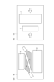
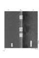
- FIG. 1 is a schematic perspective view showing a small integrated laser device including the laser element according to the embodiment.
- FIG. 2A is a diagram illustrating a method for manufacturing a laser element according to an embodiment.
- FIG. 2B is a diagram illustrating a continuation of FIG. 2A.
- FIG. 3A is a diagram illustrating a continuation of FIG. 2B.
- FIG. 3B is a diagram illustrating a continuation of FIG. 3A.
- FIG. 4 is a diagram illustrating a continuation of FIG. 3 (b).
- FIG. 5A is a diagram showing the periphery of the junction portion of the junction element according to the embodiment.
- FIG. 5B is an enlarged view showing the inside of the broken line frame of FIG. 5A.
- FIG. 6A is a diagram showing the periphery of the joint portion of the laser element according to the embodiment.
- FIG. 6B is an enlarged view showing the inside of the broken line frame of FIG. 6A.
- FIG. 7A is a diagram showing the periphery of the junction portion of the junction element according to the embodiment.
- FIG. 7B is a graph showing the elements detected within the frame of FIG. 7A.
- FIG. 8A is a diagram showing the periphery of the joint portion of the laser element according to the embodiment.
- FIG. 8B is a graph showing the elements detected in the frame of FIG. 8A.
- FIG. 9A is a diagram showing the periphery of the joint portion of the laser element according to the embodiment.
- FIG. 9B is a graph showing the elements detected in the frame of FIG. 9A.
- FIG. 10A is a diagram showing the periphery of the joint portion of the laser element according to the embodiment.
- FIG. 10B is a graph showing the elements detected within the frame of FIG. 10A.
- FIG. 11A is a diagram showing the periphery of the joint portion of the laser element according to the embodiment.
- FIG. 11B is a graph showing the elements detected in the frame of FIG. 11A.
- FIG. 12 is a diagram showing the periphery of the junction portion of the junction element according to the embodiment.
- FIG. 13 is a diagram showing the periphery of the joint portion of the laser element according to the embodiment.
- FIG. 14 is a diagram showing the periphery of the joint portion of the laser element according to the embodiment.
- FIG. 15 is a cross-sectional view showing a laser element according to a modified example.
- FIG. 16 is a diagram showing the periphery of the junction portion of the junction element, which is an element before the temperature rise step.
- FIG. 17 is a diagram showing the periphery of the joint portion of the laser element, which is the element after the temperature raising step.
- FIG. 18 is a diagram showing the periphery of the joint portion of the laser element, which is the element after the temperature raising step.
- FIG. 19 is a graph showing the elements detected at the positions shown in FIG. 18 in the scanning direction.
- FIG. 20 is a diagram showing the periphery of the junction portion of the junction element, which is an element before the temperature rise step.
- FIG. 21 is a graph showing the elements detected at the positions shown in FIG. 20 in the scanning direction.
- FIG. 22 is a diagram showing the periphery of the junction portion of the junction element after the EB irradiation, which is the element before the temperature rise step.
- FIG. 1 is a schematic perspective view showing a small integrated laser device 100.
- the compact integrated laser device 100 shown in FIG. 1 is a laser light source that emits laser light L, and constitutes a power laser that is smaller, simpler, and has higher output than a fiber laser or a disk laser.
- the small integrated laser device 100 includes the laser element 1 according to the embodiment.
- the emission direction (traveling direction) of the laser beam L will be described as the “Z direction”.
- the cross section shown in FIGS. 2 and 2 is an XY cross section, and the in-plane horizontal axis is the “X direction” and the in-plane vertical axis is the “Y direction”.
- the dimensional ratios in the drawings are not limited to the ratios shown.
- the laser element 1 is an optical element having a DFC structure.
- the laser element 1 includes a plurality of heat sinks 2, a plurality of laser media 3, a first coating layer 4a, a second coating layer 5, and a third coating layer 4b.
- the laser element 1 can form a high-power microlaser.
- the laser element 1 when the diode light of continuous oscillation having a wavelength of 808 nm is input as the excitation light I from one end side (left side in the drawing) in the Z direction along the Z direction, the laser light L having a wavelength of 1064 nm is generated. It is emitted from the other end side (right side in the drawing) in the Z direction via the Q-switch element 8 made of a saturable absorber.
- the laser element 1 is not provided with the Q-switch element 8, it is possible to configure a CW (Continuous Wave) laser.
- the heat sink 2 and the laser medium 3 have a rectangular plate shape with the Z direction as the thickness direction.
- the heat sink 2 has a flat plate shape having a thickness of 1 mm, a vertical dimension of 10 mm, and a horizontal dimension of 10 mm.
- the laser medium 3 has a flat plate shape having a thickness of 1 mm, a vertical dimension of 8 mm, and a horizontal dimension of 8 mm.
- the heat sink 2 and the laser medium 3 may have a circular plate shape.
- the heat sink 2 and the laser medium 3 are arranged so as to be alternately arranged along the Z direction. That is, the laser medium 3 is located between the pair of adjacent heat sinks 2.
- the heat sink 2 and the laser medium 3 are joined (directly joined) without using an adhesive.
- the portion from the laser medium 3 arranged on the one end side to the laser medium 3 arranged on the other end side in the Z direction functions as a resonator.
- the heat sink 2 is a substance having a thermal conductivity similar to or higher than that of the laser medium 3.
- the heat sink 2 has a function of dissipating heat from the laser medium 3.
- the heat sink 2 constitutes the first element portion.
- the heat insulating material 2 is a garnet containing diamond, silicon carbide, sapphire, YAG, vanadate, sex oxide, floride, apatite, tongue state, silicate, phosphoric acid-based material, laser material to which rare earth ion or transition metal is added, and optical switch material. , Non-linear optical material, or functional optical material.
- the vanadate is, for example, YVO 4 or LuVO 4 .
- the heat sink 2 is an example of the first element portion, and the first element portion is not limited to the heat sink 2.
- the state of the first element unit may be single crystal, amorphous (including glass), or ceramics.
- the laser medium 3 is a substance that amplifies light in an excited state by forming a population inversion that exceeds the loss and amplifies light by utilizing stimulated emission.
- the laser medium 3 is also referred to as a gain medium.
- the laser medium 3 constitutes a second element unit.
- the laser medium 3 includes diamond, silicon carbide, sapphire, garnet containing YAG, vanadate, sex oxide, flolide, apatite, tongue state, silicate, phosphoric acid-based material, laser material to which rare earth ions or transition metals are added, and an optical switch.
- the semiconductor is, for example, ZnS or ZnSe.
- the laser medium 3 is an example of the second element portion, and the second element portion is not limited to the laser medium 3.
- the state of the second element portion may be single crystal, amorphous (including glass), or ceramics.
- the heat sink 2 and the laser medium 3 are transparent to the emitted laser beam L.
- Transparent to the laser light L means that the laser light L is transmitted, and specifically, it means that the laser light L passes through while maintaining the intensity.
- transmission here means that the transmittance (net transmittance after deducting the Fresnel loss) with respect to the laser beam L is 95% or more, specifically, 97% or more. This is the same for the following transparency.
- the first coating layer 4 is a dielectric multilayer film formed on the surface (surface in contact with the atmosphere) on one end side of the heat sink 2 on one end side in the Z direction.
- the first coating layer 4 has a reflection characteristic that is non-reflective with respect to the excitation light I and highly reflected with respect to the laser light L. According to the first coating layer 4, the fluctuation of the refractive index between the heat sink 2 on one end side and the atmosphere can be suppressed.
- the second coating layer 5 is a dielectric multilayer film formed on the surface of the other end side (the surface in contact with the atmosphere) of the heat sink 2 on the other end side in the Z direction.
- the second coating layer 5 has a high reflection property for the excitation light I and a partial reflection property for the laser light L. According to the second coating layer 5, the fluctuation of the refractive index between the heat sink 2 on the other end side and the atmosphere can be suppressed.
- various other coating layers may be appropriately provided on the heat sink 2 and the laser medium 3. Thereby, the reflection characteristics at each interface of the heat sink 2 and the laser medium 3 can be appropriately adjusted.
- the laser element 1 includes a crystallization layer 6, and the crystallization layer 6 is a buffer layer interposed between the heat sink 2 and the laser medium 3.
- the laser element 1 is a crystallized layer, that is, a layer in a crystalline state.
- a crystal is a solid substance having a spatially periodic atomic arrangement.
- a crystal is a substance in which atoms and molecules are spatially arranged in a repeating pattern.
- a crystal is a substance having discrete spatial translational symmetry.
- the crystals here include quasicrystals.
- the crystallization layer 6 is a layer in which the elements constituting the heat sink 2 gradually decrease (gradually decrease) and the elements constituting the laser medium 3 gradually increase (gradually increase) from the heat sink 2 side to the laser medium 3 side. (See FIGS. 8 to 11).
- the crystallization layer 6 is integrated with the heat sink 2 and the laser medium 3.
- the crystallization layer 6 is transparent to the laser light L and transmits the laser light L.
- heat sink material and the laser medium material examples include the combinations shown in Table 1 below.
- RE is an added rare earth element such as Ce, Pr, Nd, Sm, Eu, Tb, Dy, Ho, Er, Tm, Yb.
- TM is an added transition metal element such as Mg, Ca, Mn, Fe, Co, Ni, Cu, Zn, Cr, Ti, Te, Nb and V.
- the heat sink and the laser medium may be optically coated before joining.
- a plurality of heat sinks 2 and a plurality of laser media 3 are prepared.
- the first coating layer 4 and the second coating layer 5 are appropriately formed on the heat sink 2.
- Various known film forming methods can be adopted for the film forming.
- the heat sink 2 and the laser medium 3 are arranged so as to be alternately arranged, and the heat sink 2 and the laser medium 3 are directly bonded via the amorphous layer 16 to form a bonding element. obtain.
- a temperature raising step at least a part of the amorphous layer 16 is crystallized by raising the temperature of the bonding element.
- 2 (a), 2 (b) and 3 (a) are diagrams for explaining the joining step.
- 3 (b) and 4 are diagrams for explaining the heating step.
- joining of one heat sink 2 and one laser medium 3 will be illustrated. Further, the heat sink 2 and the laser medium 3 are shown in a cross section along the line AA of FIG. 1, but the cross section is not hatched (the same applies to other cross-sectional views).
- the heat sink 2 and the laser medium 3 are arranged in the chamber 11, and the inside of the chamber 11 is a substantially vacuum environment.
- the heat sink 2 and the laser medium 3 are joined by surface active bonding.
- surface active bonding the oxide film or surface deposits on the bonding surface of the material to be bonded in vacuum are removed by ion beam irradiation or FAB (high-speed atomic beam) irradiation, and the bonding surfaces that are flat and exposed of constituent atoms are bonded to each other. It is a method of doing.
- Surface active bonding is a direct bonding using an intermolecular bond. Surface active bonding can significantly reduce the bonding temperature compared to other bonding methods.
- the surface of the heat sink 2 on the junction side and the surface of the laser medium 3 on the junction side are irradiated with an ion beam such as argon (Ar) or FAB (high-speed atomic beam).
- an ion beam such as argon (Ar) or FAB (high-speed atomic beam).
- Ar argon
- FAB high-speed atomic beam
- oxygen and the like adsorbed on the surface are removed, and a new surface containing a dangling bond is formed.
- the substantially vacuum environment is, for example, a vacuum or decompression atmosphere having a background pressure of 1 ⁇ 10-6 Pa or more and less than atmospheric pressure.
- a rare gas or an inert gas such as neon (Ne), krypton (Kr), xenon (Xe), or helium (He) can be adopted. Since the rare gas does not easily cause a chemical reaction, it does not significantly change the chemical properties of the irradiated surface.
- a predetermined kinetic energy can be given to the ion beam or the FAB.
- the bonding side of the heat sink 2 and the bonding side of the laser medium 3 are opposed to each other.
- the newly exposed surfaces of the heat sink 2 and the laser medium 3 are brought into contact with each other in a substantially vacuum environment.
- a bonding force is generated due to the interaction between atoms, and the heat sink 2 and the laser medium 3 are firmly bonded to each other via the amorphous layer 16.
- the substantially vacuum environment is, for example, a vacuum or a reduced pressure atmosphere having a background pressure of 1.5 ⁇ 10-6 Pa or less.
- a predetermined pressure (1.5 to 2.0 MPa) may be applied to the heat sink 2 and the laser medium 3 in contact with each other.
- the amorphous layer 16 is a layer in an amorphous state.
- the amorphous layer 16 is a buffer layer interposed between the heat sink 2 and the laser medium 3 in the bonding element 10.
- Amorphous is a substance that does not have long-range order like crystals, but has short-range order.
- Amorphous is a substance in which the crystal structure is broken.
- the amorphous layer 16 is a layer having a crystallinity lower than a certain level.
- the amorphous layer 16 is transparent to the laser beam L and transmits the laser beam L.
- the amorphous layer 16 contains, as impurities other than the substances constituting the heat sink 2 and the laser medium 3, the beam source element constituting the ion beam or FAB, and the beam housing material constituting the beam housing of the ion beam or FAB. including.
- the beam source element is, for example, Ar (argon) or Ne (neon).
- the beam housing material is, for example, Fe (iron), Ni (nickel) or Cr (chromium).
- the amount of the beam source element contained in the amorphous layer 16 is so small that it does not affect the oscillation of the laser beam L.
- the joining element 10 is arranged in the heating furnace 14, the joining element 10 is heat-treated, and the joining element 10 is heated to a predetermined temperature. As a result, the bonding element 10 is annealed, and the amorphous layer 16 of the bonding element 10 is epitaxially grown and crystallized. As a result, the laser element 1 shown in FIG. 4 is obtained.
- the predetermined temperature for raising the temperature (also referred to as crystallization temperature or epi-growth temperature) is a temperature lower than the melting points of the heat sink 2 and the laser medium 3.
- the predetermined temperature for raising the temperature is 100 ° C. or higher and lower than the melting point of the substance constituting the amorphous layer 16.
- the predetermined temperature for raising the temperature is about 865 ° C, which is about half of the melting points of the heat sink 2 and the laser medium 3 of about 2000 ° C.
- the predetermined temperature for raising the temperature is 1900 ° C. or lower, which is the melting point of the uncoated garnet.
- a coating for example, an optical coating layer 12 (see FIG.
- the predetermined temperature for raising the temperature is a low temperature that does not affect the coating, and is 200 ° C. or 300 ° C. And so on.
- the heating time of the bonding element 10 is, for example, several hours to several tens of hours.
- the predetermined temperature for raising the temperature may be 100 ° C. or lower.
- the melting point for each material for example, the temperature shown in Table 2 can be mentioned.
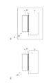
- FIG. 5A is a diagram showing the periphery of the junction portion of the junction element 10 which is an element before the temperature rise step.
- FIG. 5B is an enlarged view showing the inside of the broken line frame of FIG. 5A.
- sapphire is used for the heat sink 2 and Nd: YAG is used for the laser medium 3 (hereinafter, Nd: YAG in the figure is also simply referred to as “YAG”).
- Nd YAG in the figure is also simply referred to as “YAG”).
- the figures of FIGS. 5 (a) and 5 (b) are EDX (Energy dispersive X-ray spectroscopy) data (the same applies to FIGS. 6 to 14 below).
- FIGS. 5A and 5B it can be confirmed that the amorphous layer 16 is interposed between the heat sink 2 and the laser medium 3 in the bonding element 10.
- FIG. 6A is a diagram showing the periphery of the junction portion of the laser element 1 which is the element after the temperature raising step.
- FIG. 6B is an enlarged view showing the inside of the broken line frame of FIG. 6A.
- the laser element 1 of FIGS. 6A and 6B is obtained by heating the bonding element 10 at 1000 ° C. for 3 hours.
- the amorphous layer 16 crystallizes in the temperature raising step, and the crystallized layer 6 is between the heat sink 2 and the laser medium 3. Can be confirmed to be intervening.
- the boundary between the heat sink 2 and the laser medium 3 exists clearly (clearly).
- the amorphous layer 16 has an interface E1 with the heat sink 2.
- the crystallized layer 6 formed by crystallizing the amorphous layer 16 has an interface E2 between the amorphous layer 16 and the heat sink 2.
- the flatness of the interface E2 is higher than the flatness of the interface E1.
- Flatness can be defined, for example, as the magnitude of deviation from a plane. Flatness can be expressed, for example, by the distance between the most protruding and most recessed parts.
- FIG. 7A is a diagram showing the periphery of the junction portion of the junction element 10 which is an element before the temperature rise step.
- FIG. 7B is a graph showing the elements detected within the frame of FIG. 7A.
- the vertical axis is the amount of measurement signal corresponding to the quantity of elements, and the horizontal axis is the scan distance.
- the scanning direction of the graph of FIG. 7 (b) corresponds to the direction from top to bottom in FIG. 7 (a).
- the description of the graph in FIG. 7 (b) is the same for FIGS. 8 (b), 9 (b) and 10 (b).
- the elements constituting the heat sink 2 gradually decrease from the heat sink 2 side to the laser medium 3 side, and the elements constituting the heat sink 2 gradually decrease. It can be confirmed that the elements constituting the laser medium 3 are gradually increasing. Further, it can be confirmed that Fe and Ar are slightly contained as impurities other than the substances constituting the heat sink 2 and the laser medium 3 in the range (25 nm to 40 nm) where the amorphous layer 16 exists.
- FIG. 8A is a diagram showing the periphery of the junction portion of the laser element 1 which is the element after the temperature raising step.
- FIG. 8B is a graph showing the elements detected in the frame of FIG. 8A.
- the laser element 1 of FIGS. 8A and 8B is obtained by heating the bonding element 10 at 1000 ° C. for 3 hours.
- the elements constituting the heat sink 2 gradually decrease from the heat sink 2 side to the laser medium 3 side, and the laser It can be confirmed that the elements constituting the medium 3 are gradually increasing.
- FIG. 9A is a diagram showing the periphery of the junction portion of the laser element 1 which is the element after the temperature raising step.
- FIG. 9B is a graph showing the elements detected in the frame of FIG. 9A.
- the laser element 1 of FIGS. 9A and 9B is obtained by heating the bonding element 10 at 1000 ° C. for 3 hours.
- the result of FIG. 9B is a higher resolution analysis result than the result of FIG. 8B.
- the elements constituting the heat sink 2 gradually decrease from the heat sink 2 side to the laser medium 3 side, and the laser It can be confirmed that the elements constituting the medium 3 are gradually increasing.
- FIG. 10A is a diagram showing the periphery of the joint portion of the laser element 1 which is the element after the temperature raising step.
- FIG. 10B is a graph showing the elements detected within the frame of FIG. 10A.
- the laser element 1 of FIGS. 10A and 10B is obtained by heating the bonding element 10 at 1000 ° C. for 3 hours.
- the results of FIG. 10 (b) show C (carbon), Ar and Fe among the results of FIG. 9 (b).
- the graph of FIG. 10 (b) is superimposed on the position corresponding to the distance of FIG. 10 (b) on FIG. 10 (a).
- FIG. 11A is a diagram showing the periphery of the junction portion of the laser element 1 which is the element after the temperature raising step.
- FIG. 11B is a graph showing the elements detected in the frame of FIG. 11A.
- the laser element 1 of FIGS. 11A and 11B is obtained by heating the bonding element 10 at 1000 ° C. for 3 hours.
- the result of FIG. 11B is a higher resolution analysis result than the result of FIG. 8B.
- the vertical axis is the amount of measurement signal corresponding to the quantity of elements
- the horizontal axis is the scan distance.
- the scanning direction of the graph in FIG. 11B corresponds to the direction from top to bottom in FIG. 11A. As shown in FIG.
- the elements constituting the heat sink 2 in the range where the crystallized layer 6 exists (85 nm to 95 nm), gradually decrease from the heat sink 2 side to the laser medium 3 side, and the laser It can be confirmed that the elements constituting the medium 3 are gradually increasing.
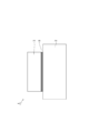
- FIG. 12 is a diagram showing the periphery of the junction portion of the junction element 10 which is an element before the temperature rise step.
- sapphire was used for the heat sink 2 and ceramic YAG was used for the laser medium 3 (the same applies to FIGS. 13 and 14 below).
- the amorphous layer 16 having a thickness of 7 nm or less is interposed between the heat sink 2 and the laser medium 3. Further, here, the unknown layer Q exists near the interface between the heat sink 2 and the laser medium 3.
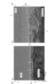
- FIG. 13 is a diagram showing the periphery of the joint portion of the laser element 1 which is an element after the temperature raising step.
- the laser element 1 of FIG. 13 is obtained by heating the bonding element 10 at 100 ° C. for 10 hours.
- crystallization of the amorphous layer 16 is in progress. As shown in FIG. 13, it can be confirmed that the crystallization layer 6 is interposed between the heat sink 2 and the laser medium 3.
- the crystallization layer 6 is formed in a layered state including a plurality of layers.
- the crystallization layer 6 includes a 2.6 nm layer, a 1.7 nm layer, and a 2.2 nm layer from the heat sink 2 side toward the laser medium 3 side at a certain position.
- the crystallization layer 6 includes a 2.6 nm layer, a 2.0 nm layer, and a 1.7 nm layer from the heat sink 2 side toward the laser medium 3 side at other points.
- the crystallization layer 6 includes a 2.6 nm layer, a 1.7 nm layer, and a 2.0 nm layer from the heat sink 2 side toward the laser medium 3 side at still other points.
- the coefficient of progress of crystallization is 0.5 nm / h.
- FIG. 14 is a diagram showing the periphery of the joint portion of the laser element 1 which is an element after the temperature raising step.
- the laser element 1 of FIG. 14 is obtained by heating the bonding element 10 at 100 ° C. for 24 hours.
- the crystallization of the amorphous layer 16 is more advanced. As shown in FIG. 14, it can be confirmed that the crystallization layer 6 is interposed between the heat sink 2 and the laser medium 3.
- the crystallization layer 6 includes a 1.8 nm layer and a 3.4 nm layer from the heat sink 2 side toward the laser medium 3 side at a certain location.
- the crystallization layer 6 includes a 3.1 nm layer and a 1.7 nm layer from the heat sink 2 side toward the laser medium 3 side at other points.
- the crystallization layer 6 includes a 3.3 nm layer and a 1.7 nm layer from the heat sink 2 side toward the laser medium 3 side at still other points.
- the coefficient of progress of crystallization is 0.5 nm / h.
- the amorphous layer 16 is epitaxially grown by raising the temperature of the bonding element 10, the amorphous layer 16 is crystallized, and the material state (bonding state) of the laser element 1 is stabilized.
- the bonding characteristics can be improved without deteriorating the characteristics of the bonding portion.
- the bonding step at least one of the surface on the bonding side of the heat sink 2 and the surface on the bonding side of the laser medium 3 is irradiated with an ion beam or a high-speed atomic beam in a substantially vacuum environment.
- the bonding element 10 can be obtained by bringing the surface of the heat sink 2 on the bonding side into contact with the surface of the laser medium 3 on the bonding side.
- the temperature raising step there is a concern that stress is generated at the joint portion due to the difference in the coefficient of linear expansion, causing damage such as peeling to the laser element 1.
- the amorphous layer 16 contains the beam source element constituting the ion beam or the high-speed atomic beam and / or impurities of the beam housing material
- the temperature required for epitaxial growth at the time of temperature rise is set to the heat sink 2. And it is found that the temperature can be lowered to a predetermined temperature much lower than the melting point of the laser medium 3.
- the amorphous layer 16 contains the beam source element and / or the beam housing material, and the temperature of the temperature rise is lowered to a predetermined temperature lower than the melting points of the heat sink 2 and the laser medium 3. ing. Therefore, it is possible to suppress the damage of the laser element 1. Since the crystallized layer 6 does not require a high temperature for the solid-phase reaction, ideal crystal growth with less distortion is possible.
- the heat sink 2 is formed of diamond, silicon carbide, sapphire, garnet containing YAG, vanadate, laser material to which rare earth ion or transition metal is added, optical switch material, nonlinear optical material, functional optical material, Or it is ceramics.
- the laser medium 3 is a laser material to which diamond, silicon carbide, sapphire, garnet containing YAG, vanadate, rare earth ion or transition metal is added, an optical switch material, a nonlinear optical material, a functional optical material, or a ceramic.
- the predetermined temperature which is the temperature at which the temperature is raised (epi growth temperature), is 100 ° C. or higher and 1100 ° C. or lower. With respect to the laser element 1 provided with such a heat sink 2 and a laser medium 3, it is possible to stabilize the material state of the laser element 1 by raising the temperature and suppress damage to the laser element 1 at the time of raising the temperature. ..
- the ceramics include those having a Faraday effect such as TGG (terbium gallium garnet), TAG (terbium aluminum garnet), and TSAG (terbium scandium aluminum garnet) ceramics. Ceramics are vulnerable to damage due to grain boundaries at the end faces, and must be joined and used for protection. Since ceramics cannot be made to a thickness of about 10 mm, joining is indispensable when using a thick material. When ceramics are bonded, it is desirable to stabilize them by a temperature raising step (annealing treatment) because the bonding boundary material is unstable.
- annealing treatment a temperature raising step
- a crystallized layer 6 is interposed between the heat sink 2 and the laser medium 3 instead of the amorphous layer 16, and the crystallized layer 6 moves from the heat sink 2 side to the laser medium 3 side.
- the elements constituting the heat sink 2 gradually decrease, and the elements constituting the laser medium 3 gradually increase. According to such a configuration, it is possible to stabilize the material state of the laser element 1.
- the amorphous layer 16 the element changes relatively slowly, but in the crystallized layer 6, the change of the element becomes steep.
- FIG. 15 is a cross-sectional view showing the laser element 101 according to the modified example.
- the optical coating layer 12 is formed on the surface of the heat sink 2 by applying an optical coating to the surface of the heat sink 2.
- the optical coating is not particularly limited, and various known optical coatings can be adopted.
- the optical coating layer 12 is a part of the heat sink 2 and constitutes the surface side of the heat sink 2. That is, the heat sink 2 has an optical coating layer 12 on the joint side portion thereof.
- the heat sink 2 is not limited to the heat sink 2, and other laser materials may be used, an optical switch such as Cr: YAG may be used, or a crystal, LN, LBO, KTP, GaAs, It may be a nonlinear optical crystal such as GaP, ZnSe, ZnS.
- a layer that becomes transparent by temperature rise treatment that is, a semiconductor material such as Si, Ga, Zn, or Si, Al, Ti, Hf, Mg, Zr, Ta, Nb is deposited. Sometimes it makes me.
- the final layer of the optical coating layer 12 has a layer that becomes transparent by the temperature raising treatment. After joining the heat sink 2 and the laser medium 3, the layer that becomes transparent due to the temperature rise treatment becomes an oxide or compound by heat treatment in an oxygen atmosphere or the like as an appropriate environment, and is sufficiently transparent in the desired laser wavelength range. To serve its function.
- an optical coating is applied to the surface of the heat sink 2, and the heat sink 2 and the laser medium 3 are bonded by surface active bonding to form a bonding element.
- the bonded element is heat-treated to raise the temperature of the bonded element to a predetermined temperature.
- the bonding element is annealed, and the amorphous layer of the bonding element is epitaxially grown and crystallized, resulting in the laser element 101 shown in FIG.
- the predetermined temperature for raising the temperature is lower than the melting points of the heat sink 2 and the laser medium 3.
- the predetermined temperature for raising the temperature is 100 ° C. or higher and 600 ° C. or lower.
- the heat sink 2 has an optical coating layer 12 on the joint side portion thereof, and the predetermined temperature for raising the temperature is 100 ° C. or higher and 600 ° C. or lower. .. Deterioration of the optical coating layer 12 is observed when the temperature is raised to about 800 ° C. or higher. Therefore, in the method for manufacturing the laser element 101 according to the modified example, damage to the optical coating layer 12 can be suppressed. Recrystallization, that is, epi-growth, is possible by raising the temperature at a sufficiently low temperature so that the optical coating layer 12 is not damaged.
- the laser medium 3 may have an optical coating layer on the junction side portion thereof, or both the heat sink 2 and the laser medium 3 may have an optical coating layer on the junction side portion thereof.
- the predetermined temperature for raising the temperature may be 800 ° C. or lower, 200 ° C. to 300 ° C., 100 ° C., or higher than the joining temperature.
- the heat sink 2 is made of SiC or diamond, the optical coating layer 12 is particularly effective because the refractive indexes are significantly different.
- the junction temperature is preferably the temperature at which the substance is used.
- the final layer a layer that becomes transparent by temperature rise treatment, that is, a semiconductor material such as Si, Ga, Zn, or Si, Al, Ti, Hf, Mg, Zr, Ta, Nb is deposited. Sometimes it makes me.
- the final layer of the optical coating layer has a layer that becomes transparent by the temperature raising treatment.
- the layer that becomes transparent due to the temperature rise treatment becomes an oxide or compound by heat treatment in an oxygen atmosphere or the like as an appropriate environment, and is sufficiently transparent in the desired laser wavelength range. To serve its function.
- the following effects are also achieved. That is, it is possible to join not only the same kind of materials but also different kinds of materials that are generally difficult to join. Any material such as metal, glass and film can be bonded. It does not take heat and can suppress deformation due to heat. No adhesive is required. The joint strength can be controlled. Not only strong bonding but also temporary bonding assuming peeling can be supported. Since the joining time is short, the joining can be completed in seconds in principle. There is no deviation after joining, and high alignment accuracy can be achieved.
- Nd YAG
- Cr YAG as the passive Q-switch medium
- Nd: YAG is usually shortened in order to shorten the resonator.
- a highly reflective coating regarding the excitation wavelength is applied to the surface opposite to the excitation side (the boundary surface of Cr: YAG) to halve L 0 .
- the coating layer interferes and cannot be joined.
- the bonded insert made of ceramic YAG is generally long, and the obtained pulse width is also long. That is, only laser light sources with low performance and weak competitiveness can be made.
- a microchip capable of generating a short pulse width can be expected from the ceramic YAG. Since it is possible to join a large area, the ceramic YAG composite can be mass-produced and the cost can be reduced by molding a large area at once and cutting it into small chips. In particular, in the present embodiment, it is possible to further increase the area and join with a higher joining strength, and the mass production effect and cost reduction due to the larger size are remarkable. It is possible to manufacture optical elements with high performance and high reliability.
- each of the above numerical values may include errors in design, measurement, manufacturing, and the like.
- the laser element 1 according to one embodiment of the present invention can be applied to various laser components and thus to a laser device, and the laser device can be used in various devices such as a measuring device, a processing device, a diagnostic device, and a medical device. ..
- the entire amorphous layer 16 is crystallized by raising the temperature of the bonding element 10 in the temperature raising step, but the entire amorphous layer 16 is not limited to crystallizing. At least a part of the amorphous layer 16 may be crystallized.
- the amorphous layer 16 may be a mixed crystal system of Si and YAG, or a mixed crystal system of Si and sapphire. These melting points are very high, about 2000 ° C., but the predetermined temperature, which is the epi growth temperature, is much lower than that.
- One embodiment of the present invention may include a spatial modulation element that controls the spatial mode of the laser beam.
- the spatial modulation element may or may not be bonded to the heat sink 2 and the laser medium 3. This makes it possible to configure a high-luminance and high-output microamplifier.
- the first element portion and the second element portion are surface-actively bonded, but in the surface-active bonding, it is not necessary to create a substantially vacuum environment when the heat sink 2 and the laser medium 3 are brought into contact with each other.
- the second element portion is gold (Au), copper (Cu), copper tungsten (CuW), aluminum (Al), iron (Fe), titanium (Ti), or any of these. It may be a metal containing at least any alloy.
- the optical element according to one embodiment of the present invention can be applied to any optical element as long as it is an optical element that transmits, reciprocates, or reflects laser light.
- the optical element according to one embodiment of the present invention is not limited to an oscillator, but also includes an amplifier, a functional optical material (Q-switch element such as Cr: YAG), a nonlinear optical material, and a wavelength conversion element such as QPM-crystal.
- the material to be bonded may be not only a combination of a laser medium and a heat sink, but also an optical switch such as a saturable absorber, a nonlinear optical material for wavelength conversion, and the like.
- the transmittance of transparency does not necessarily have to be 95% or more.
- the configuration bonded via the crystallization layer is not particularly limited to those described above, and may be, for example, the optical elements of the following configuration examples 1 to 4.
- the laser medium is, for example, RE: single crystal / ceramics (YAG, YSGG, YLF, YVO 4 , SFAP, etc.), RE: glass.
- the Q-switch element is, for example, Cr: YAG.
- the transparent heat sink is, for example, YAG, sapphire, SiC, or diamond.
- (Configuration Example 2) An optical element including a transparent heat sink, a laser medium laminated on the heat sink, and a crystallization layer between them. (Configuration Example 3) Between the transparent heat sink, the laser medium laminated on the transparent heat sink, the Q-switch element laminated on the laser medium, the crystallization layer between the transparent heat sink and the laser medium, and between the laser medium and the Q-switch. An optical element including a crystallized layer. (Configuration Example 4) Between the transparent heat sink, the laser medium laminated on the transparent heat sink, the Q-switch element laminated on the laser medium, the transparent heat sink laminated on the Q-switch, the transparent heat sink, and the laser medium adjacent thereto. An optical element including a crystallization layer, a crystallization layer between a laser medium and a Q-switch, and a crystallization layer between a Q-switch element and a transparent heat sink adjacent thereto.
- a known coating layer may be appropriately provided on each member (first element portion and second element portion) constituting the optical element. Since the refractive indexes of Nd: YAG and Cr: YAG are substantially the same, direct bonding via a crystallization layer is possible without requiring an AR (Anti Reflection) coating as a coating layer. However, in order to improve the excitation efficiency, an HR (High Reflection) coating having a target wavelength of 808 nm or 885 nm and an AR coating having a target wavelength of 1064 nm may be provided as the coating layer.
- an HR High Reflection
- one embodiment of the present invention includes variations such as a configuration in which a coating (optical coating) is applied and bonded to the coating (optical coating) via a crystallization layer.
- the transparent first element portion and the second element portion include an optical switch element such as a transparent Q-switch element when the switch is ON.
- the combination of element parts to be joined is an optical gain medium, Q switch element, heat sink (YAG, sapphire, SiC, diamond, opaque material such as Al, Cu, CuW), nonlinear optical element (nonlinear wavelength conversion (SHG)). , Raman element, etc.), nonlinear optical switch, etc.), wave plate, polarizer, beam splitter, beam coupling element, etc., which may be an appropriate combination.
- the Q-switch element includes not only conventional AO (Acousto Optic) and EO (Electro Optic) but also MO (Magneto Optic).
- a wave plate or a polarizer may be arranged inside the resonator for bonding.
- a nonlinear optical wavelength conversion element may be included, or a beam splitter or a beam coupling element may be included.
- the excitation light may be introduced from the heat sink. Joining a transparent heat sink is also effective in preventing parasitic oscillation.
- metal is used as the heat sink.
- the metal is Al or an alloy thereof, and further, when only the outermost surface portion of the heat sink is Al or the like, the laser medium is coated with HR for the emitted laser light, and then the heat sink is joined by some method.
- an alumina layer is sputtered or vapor-deposited on the outside of the HR coat, and then both are sandwiched between anvils or the like, and a giant pulse laser beam having a different wavelength transmitted through the HR coat is irradiated therein to form an element forming a heat sink. It is also effective to mix the elements constituting the laser medium and the elements constituting the laser medium non-thermally at the crystal level to bond them.
- FIG. 16 is a diagram showing the periphery of the junction portion of the junction element 10 which is an element before the temperature rise step.
- Nd YAG ceramics were used for the heat sink 2
- Nd YAG single crystal was used for the laser medium 3 (the same applies to FIGS. 17 to 22 below).
- the figure of FIG. 16 is EDX data (the same applies to FIGS. 17 and 22 below).
- the amorphous layer 16 is interposed in the bonding element 10 before the temperature raising step (before the annealing treatment).
- the amorphous layer 16 has a thickness of 10 to 15 nm.
- FIG. 17 is a diagram showing the periphery of the joint portion of the laser element 1 which is an element after the temperature raising step. As shown in FIG. 17, it can be confirmed that the amorphous layer 16 (see FIG. 16) has disappeared in the laser element 1 after the temperature raising step (after the annealing treatment). Nd: The expansion of the region of the YAG single crystal (epitaxial growth) can be verified.
- FIG. 18 is a diagram showing the periphery of the joint portion of the laser element 1 which is an element after the temperature raising step.
- FIG. 19 is a graph showing the elements detected at the positions shown in FIG. 18 in the scanning direction.
- FIG. 20 is a diagram showing the periphery of the junction portion of the junction element 10 which is an element before the temperature rise step.
- FIG. 21 is a graph showing the elements detected at the positions shown in FIG. 20 in the scanning direction.
- FIGS. 18 and 20 are bright-field images which are STEM images created by detecting electrons that are transmitted without being scattered and electrons that are scattered at a small angle among the transmitted electrons. ..
- the vertical axis represents the amount of measurement signal corresponding to the quantity of elements
- the horizontal axis represents the scan distance.
- the scanning direction of the graph in FIG. 19 corresponds to the direction from top to bottom in FIG.
- the scanning direction of the graph in FIG. 21 corresponds to the direction from top to bottom in FIG.
- FIGS. 18 to 21 it is confirmed that the elements constituting the heat sink 2 gradually decrease and the elements constituting the laser medium 3 gradually increase, for example, from the heat sink 2 side to the laser medium 3 side. it can.
- FIG. 22 is a diagram showing the periphery of the bonding portion of the bonding element 10 after the EB irradiation, which is the element before the temperature rising step.
- the instability of the amorphous layer 16 at the junction interface between Nd: YAG ceramics and Nd: YAG single crystal is remarkable, and as shown in the circle frame in FIG. 22, after EB (Electron Beam) irradiation during analysis, It can be confirmed that voids are generated in the amorphous layer 16. Before EB irradiation, the amorphous layer 16 was not damaged (see FIG. 16). When the amorphous layer is crystallized by the temperature raising step (annealing treatment), such damage is not observed.
- the ceramic region which is a polycrystalline material including the bonding interface, is single-crystallized, and the ceramic-derived characteristic deterioration, such as orientation and electrons at the grain interface, is achieved. And phonon scattering are suppressed.
- a method of surface-actively bonding an arbitrary ceramic material and a single crystal and then single-crystallizing by raising the temperature is effective for improving the characteristics of the material.
- one aspect of the present invention is a ceramic region which is a polycrystal including a bonding interface by heating a single crystal to ceramics after surface active bonding. Is characterized by being single crystallized by a solid phase method below the melting point.
- one aspect of the present invention is an optical element that transmits, reciprocates, or reflects laser light, the first element portion that is transparent to the laser light, and the first element portion.
- a crystallization layer interposed between the second element portion and the first element portion and the second element portion and formed by crystallization is provided, and the crystallization layer is from the first element portion side to the second element portion side.
- the elements constituting the first element portion are continuously exchanged with the elements constituting the second element portion.
- one aspect of the present invention is an optical element that transmits, reciprocates, or reflects laser light, and is a first element portion that is transparent to the laser light.
- a crystallized layer interposed between the second element portion and the first element portion and the second element portion is provided, and at least one of the first element portion and the second element portion is joined.
- the elements constituting the first element portion or the second element portion continuously in the 10 nm region. It is replaced with the elements that make up the optical coating layer.
- At least one of the first element portion and the second element portion has an optical coating layer on the junction side portion thereof and crystallizes.
- the chemical layer contains at least one of Ar, Ne, Xe, He, Fe, Ni and Cr.
Landscapes
- Physics & Mathematics (AREA)
- Electromagnetism (AREA)
- Engineering & Computer Science (AREA)
- Chemical & Material Sciences (AREA)
- Optics & Photonics (AREA)
- Plasma & Fusion (AREA)
- Ceramic Engineering (AREA)
- Materials Engineering (AREA)
- Organic Chemistry (AREA)
- Crystallography & Structural Chemistry (AREA)
- Life Sciences & Earth Sciences (AREA)
- Chemical Kinetics & Catalysis (AREA)
- General Chemical & Material Sciences (AREA)
- Geochemistry & Mineralogy (AREA)
- Structural Engineering (AREA)
- General Physics & Mathematics (AREA)
- Lasers (AREA)
- Optical Modulation, Optical Deflection, Nonlinear Optics, Optical Demodulation, Optical Logic Elements (AREA)
- Manufacturing & Machinery (AREA)
Abstract
L'invention concerne un procédé de fabrication d'un élément optique dans lequel un faisceau laser est transmis, animé d'un mouvement de va-et-vient ou réfléchi. Le procédé comprend : une première étape consistant à obtenir un élément lié formé par soumission des première et seconde parties d'élément, qui sont transparentes au faisceau laser, à une liaison activée en surface avec une couche amorphe interposée entre celles-ci ; et, après la première étape, une seconde étape consistant à élever la température de l'élément lié de façon à cristalliser au moins une partie de la couche amorphe. Dans la seconde étape, la température de l'élément lié est élevée à une température prescrite inférieure au point de fusion des première et seconde parties d'élément.
Priority Applications (4)
| Application Number | Priority Date | Filing Date | Title |
|---|---|---|---|
| EP20826804.5A EP3989374A4 (fr) | 2019-06-18 | 2020-06-12 | Procédé de fabrication d'un élément optique et élément optique |
| US17/619,323 US11515683B2 (en) | 2019-06-18 | 2020-06-12 | Method for manufacturing optical element and optical element |
| JP2021520629A JP6955302B2 (ja) | 2019-06-18 | 2020-06-12 | 光学素子の製造方法及び光学素子 |
| CN202080044213.8A CN114008871A (zh) | 2019-06-18 | 2020-06-12 | 光学元件的制造方法及光学元件 |
Applications Claiming Priority (2)
| Application Number | Priority Date | Filing Date | Title |
|---|---|---|---|
| JP2019-113115 | 2019-06-18 | ||
| JP2019113115 | 2019-06-18 |
Publications (1)
| Publication Number | Publication Date |
|---|---|
| WO2020255880A1 true WO2020255880A1 (fr) | 2020-12-24 |
Family
ID=74040048
Family Applications (1)
| Application Number | Title | Priority Date | Filing Date |
|---|---|---|---|
| PCT/JP2020/023233 Ceased WO2020255880A1 (fr) | 2019-06-18 | 2020-06-12 | Procédé de fabrication d'un élément optique et élément optique |
Country Status (5)
| Country | Link |
|---|---|
| US (1) | US11515683B2 (fr) |
| EP (1) | EP3989374A4 (fr) |
| JP (1) | JP6955302B2 (fr) |
| CN (1) | CN114008871A (fr) |
| WO (1) | WO2020255880A1 (fr) |
Citations (6)
| Publication number | Priority date | Publication date | Assignee | Title |
|---|---|---|---|---|
| JPS6245587B2 (fr) | 1984-10-03 | 1987-09-28 | Mitsubishi Jukogyo Kk | |
| JP2003270602A (ja) * | 2002-03-18 | 2003-09-25 | Fujitsu Ltd | 亜鉛ニオブ酸鉛−チタン酸鉛混晶系強誘電体単結晶を用いた電気光学効果素子及びそれを用いた光スイッチ |
| US7515333B1 (en) * | 2002-06-13 | 2009-04-07 | Nanosy's, Inc. | Nanotechnology-enabled optoelectronics |
| JP2015210462A (ja) * | 2014-04-30 | 2015-11-24 | ブラザー工業株式会社 | 画像形成装置、画像形成装置の制御方法及び画像形成装置の制御プログラム |
| JP2017220652A (ja) * | 2016-06-10 | 2017-12-14 | 大学共同利用機関法人自然科学研究機構 | レーザ装置とその製造方法 |
| JP2019073402A (ja) * | 2017-10-12 | 2019-05-16 | 国立大学法人三重大学 | 窒化物半導体基板、窒化物半導体基板の製造方法、窒化物半導体基板の製造装置及び窒化物半導体デバイス |
Family Cites Families (15)
| Publication number | Priority date | Publication date | Assignee | Title |
|---|---|---|---|---|
| WO2003001634A1 (fr) * | 2001-06-21 | 2003-01-03 | Mitsubishi Denki Kabushiki Kaisha | Module d'excitation, oscillateur laser, et amplificateur laser |
| US6667999B2 (en) * | 2001-08-17 | 2003-12-23 | Textron Corporation | Cooling of high power laser systems |
| US20040003627A1 (en) * | 2002-07-03 | 2004-01-08 | Nihon Yamamura Glass Co., Ltd. | Locally crystallized glass |
| US7332431B2 (en) * | 2002-10-17 | 2008-02-19 | Semiconductor Energy Laboratory Co., Ltd. | Method of manufacturing semiconductor device |
| JP2005327997A (ja) * | 2004-05-17 | 2005-11-24 | Akio Ikesue | 複合レーザー素子及びその素子を用いたレーザー発振器 |
| US20060083276A1 (en) * | 2004-09-28 | 2006-04-20 | Snake Creek Lasers, Llc. | Cryogenically cooled solid state lasers |
| US7310359B2 (en) * | 2004-12-01 | 2007-12-18 | Textron Systems Corporation | Thermally self-correcting gain modules and associated systems and methods |
| US8660155B2 (en) * | 2006-02-03 | 2014-02-25 | Bae Systems Information And Electronics Systems Integration Inc. | Method and apparatus for cooling semiconductor pumped lasers |
| DE102007047014B4 (de) * | 2007-10-01 | 2019-05-02 | Robert Bosch Gmbh | Verfahren zur Herstellung einer gasdichten und hochtemperaturbeständigen Verbindung von Formteilen mittels Laser |
| JP6061251B2 (ja) * | 2013-07-05 | 2017-01-18 | 株式会社豊田自動織機 | 半導体基板の製造方法 |
| JP6228507B2 (ja) * | 2014-04-30 | 2017-11-08 | 日本電信電話株式会社 | 波長変換素子 |
| JP6152827B2 (ja) | 2014-05-16 | 2017-06-28 | 株式会社豊田自動織機 | 半導体基板の製造方法 |
| JP6393196B2 (ja) * | 2015-01-19 | 2018-09-19 | 浜松ホトニクス株式会社 | レーザ光増幅装置 |
| JP6245587B1 (ja) | 2016-10-28 | 2017-12-13 | 大学共同利用機関法人自然科学研究機構 | レーザー部品 |
| JP6632644B2 (ja) * | 2018-01-25 | 2020-01-22 | 大学共同利用機関法人自然科学研究機構 | 光学素子の製造方法及び光学素子 |
-
2020
- 2020-06-12 CN CN202080044213.8A patent/CN114008871A/zh active Pending
- 2020-06-12 WO PCT/JP2020/023233 patent/WO2020255880A1/fr not_active Ceased
- 2020-06-12 US US17/619,323 patent/US11515683B2/en active Active
- 2020-06-12 EP EP20826804.5A patent/EP3989374A4/fr active Pending
- 2020-06-12 JP JP2021520629A patent/JP6955302B2/ja active Active
Patent Citations (6)
| Publication number | Priority date | Publication date | Assignee | Title |
|---|---|---|---|---|
| JPS6245587B2 (fr) | 1984-10-03 | 1987-09-28 | Mitsubishi Jukogyo Kk | |
| JP2003270602A (ja) * | 2002-03-18 | 2003-09-25 | Fujitsu Ltd | 亜鉛ニオブ酸鉛−チタン酸鉛混晶系強誘電体単結晶を用いた電気光学効果素子及びそれを用いた光スイッチ |
| US7515333B1 (en) * | 2002-06-13 | 2009-04-07 | Nanosy's, Inc. | Nanotechnology-enabled optoelectronics |
| JP2015210462A (ja) * | 2014-04-30 | 2015-11-24 | ブラザー工業株式会社 | 画像形成装置、画像形成装置の制御方法及び画像形成装置の制御プログラム |
| JP2017220652A (ja) * | 2016-06-10 | 2017-12-14 | 大学共同利用機関法人自然科学研究機構 | レーザ装置とその製造方法 |
| JP2019073402A (ja) * | 2017-10-12 | 2019-05-16 | 国立大学法人三重大学 | 窒化物半導体基板、窒化物半導体基板の製造方法、窒化物半導体基板の製造装置及び窒化物半導体デバイス |
Non-Patent Citations (1)
| Title |
|---|
| See also references of EP3989374A4 |
Also Published As
| Publication number | Publication date |
|---|---|
| US20220271488A1 (en) | 2022-08-25 |
| EP3989374A4 (fr) | 2023-07-05 |
| CN114008871A (zh) | 2022-02-01 |
| JPWO2020255880A1 (ja) | 2021-09-30 |
| EP3989374A1 (fr) | 2022-04-27 |
| JP6955302B2 (ja) | 2021-10-27 |
| US11515683B2 (en) | 2022-11-29 |
Similar Documents
| Publication | Publication Date | Title |
|---|---|---|
| Lu et al. | Optical properties and highly efficient laser oscillation of Nd: YAG ceramics | |
| JP6245587B1 (ja) | レーザー部品 | |
| Penilla et al. | Gain in polycrystalline Nd-doped alumina: leveraging length scales to create a new class of high-energy, short pulse, tunable laser materials | |
| JP6632644B2 (ja) | 光学素子の製造方法及び光学素子 | |
| Mirov et al. | Progress in Cr2+ and Fe2+ doped mid‐IR laser materials | |
| US5563899A (en) | Composite solid state lasers of improved efficiency and beam quality | |
| JP4041782B2 (ja) | 半導体レーザ励起固体レーザ | |
| US7496125B2 (en) | Composite laser rod, fabricating method thereof, and laser device therewith | |
| WO2005112208A1 (fr) | Élément laser composite et oscillateur laser utilisant celui-ci | |
| Vatnik et al. | Thin disk Tm-laser based on highly doped Tm: KLu (WO4) 2/KLu (WO4) 2 epitaxy | |
| JP6955302B2 (ja) | 光学素子の製造方法及び光学素子 | |
| Louchet-Chauvet et al. | Piezo-orbital backaction force in a rare-earth-doped crystal | |
| US20220200231A1 (en) | Rare-earth-doped alumina-oxide laser gain media | |
| Sato et al. | Tailored Spectral Designing of Layer-by-Layer Type Composite Nd: Y $ _ {3} $ ScAl $ _ {4} $ O $ _ {12} $/Nd: Y $ _ {3} $ Al $ _ {5} $ O $ _ {12} $ Ceramics | |
| EP4418472A1 (fr) | Élément optique, dispositif laser et procédé de fabrication d'élément optique | |
| Ikesue et al. | Ceramic laser/solid‐state laser | |
| EP3787133B1 (fr) | Corps lié, oscillateur laser, amplificateur laser et procédé permettant de produire un corps lié | |
| US20240094596A1 (en) | Optical element, optical device, and method for producing optical element | |
| JP2007507084A (ja) | 固体レーザー媒質 | |
| CN118763489B (zh) | 一种基频增益与非线性频率变换一体化单晶光纤及其制备方法和应用 | |
| Huang et al. | Passively Q-switched integrated Tm: YAG/Ho: YAP laser | |
| Revankar | Metal Oxides: Solid-State Lasers | |
| JP2023175081A (ja) | 結晶型固体レーザー媒質複合体及びその製造方法 | |
| Kausas et al. | Surface Activated Bond properties of Distributed Face Cooling structure for high average power applications | |
| HIDEUR et al. | Watt-level Tm: LiYF4 channel waveguide laser produced by diamond saw dicing |
Legal Events
| Date | Code | Title | Description |
|---|---|---|---|
| 121 | Ep: the epo has been informed by wipo that ep was designated in this application |
Ref document number: 20826804 Country of ref document: EP Kind code of ref document: A1 |
|
| ENP | Entry into the national phase |
Ref document number: 2021520629 Country of ref document: JP Kind code of ref document: A |
|
| NENP | Non-entry into the national phase |
Ref country code: DE |
|
| ENP | Entry into the national phase |
Ref document number: 2020826804 Country of ref document: EP Effective date: 20220118 |