WO2020261993A1 - 電子装置及び電子装置の製造方法 - Google Patents
電子装置及び電子装置の製造方法 Download PDFInfo
- Publication number
- WO2020261993A1 WO2020261993A1 PCT/JP2020/022837 JP2020022837W WO2020261993A1 WO 2020261993 A1 WO2020261993 A1 WO 2020261993A1 JP 2020022837 W JP2020022837 W JP 2020022837W WO 2020261993 A1 WO2020261993 A1 WO 2020261993A1
- Authority
- WO
- WIPO (PCT)
- Prior art keywords
- copper
- electronic device
- bonding layer
- mass
- coating film
- Prior art date
- Legal status (The legal status is an assumption and is not a legal conclusion. Google has not performed a legal analysis and makes no representation as to the accuracy of the status listed.)
- Ceased
Links
Images

Classifications
-
- F—MECHANICAL ENGINEERING; LIGHTING; HEATING; WEAPONS; BLASTING
- F21—LIGHTING
- F21K—NON-ELECTRIC LIGHT SOURCES USING LUMINESCENCE; LIGHT SOURCES USING ELECTROCHEMILUMINESCENCE; LIGHT SOURCES USING CHARGES OF COMBUSTIBLE MATERIAL; LIGHT SOURCES USING SEMICONDUCTOR DEVICES AS LIGHT-GENERATING ELEMENTS; LIGHT SOURCES NOT OTHERWISE PROVIDED FOR
- F21K9/00—Light sources using semiconductor devices as light-generating elements, e.g. using light-emitting diodes [LED] or lasers
- F21K9/90—Methods of manufacture
-
- B—PERFORMING OPERATIONS; TRANSPORTING
- B22—CASTING; POWDER METALLURGY
- B22F—WORKING METALLIC POWDER; MANUFACTURE OF ARTICLES FROM METALLIC POWDER; MAKING METALLIC POWDER; APPARATUS OR DEVICES SPECIALLY ADAPTED FOR METALLIC POWDER
- B22F7/00—Manufacture of composite layers, workpieces, or articles, comprising metallic powder, by sintering the powder, with or without compacting wherein at least one part is obtained by sintering or compression
- B22F7/06—Manufacture of composite layers, workpieces, or articles, comprising metallic powder, by sintering the powder, with or without compacting wherein at least one part is obtained by sintering or compression of composite workpieces or articles from parts, e.g. to form tipped tools
- B22F7/08—Manufacture of composite layers, workpieces, or articles, comprising metallic powder, by sintering the powder, with or without compacting wherein at least one part is obtained by sintering or compression of composite workpieces or articles from parts, e.g. to form tipped tools with one or more parts not made from powder
-
- F—MECHANICAL ENGINEERING; LIGHTING; HEATING; WEAPONS; BLASTING
- F21—LIGHTING
- F21S—NON-PORTABLE LIGHTING DEVICES; SYSTEMS THEREOF; VEHICLE LIGHTING DEVICES SPECIALLY ADAPTED FOR VEHICLE EXTERIORS
- F21S8/00—Lighting devices intended for fixed installation
- F21S8/08—Lighting devices intended for fixed installation with a standard
- F21S8/085—Lighting devices intended for fixed installation with a standard of high-built type, e.g. street light
-
- B—PERFORMING OPERATIONS; TRANSPORTING
- B22—CASTING; POWDER METALLURGY
- B22F—WORKING METALLIC POWDER; MANUFACTURE OF ARTICLES FROM METALLIC POWDER; MAKING METALLIC POWDER; APPARATUS OR DEVICES SPECIALLY ADAPTED FOR METALLIC POWDER
- B22F3/00—Manufacture of workpieces or articles from metallic powder characterised by the manner of compacting or sintering; Apparatus specially adapted therefor ; Presses and furnaces
- B22F3/24—After-treatment of workpieces or articles
-
- B—PERFORMING OPERATIONS; TRANSPORTING
- B23—MACHINE TOOLS; METAL-WORKING NOT OTHERWISE PROVIDED FOR
- B23K—SOLDERING OR UNSOLDERING; WELDING; CLADDING OR PLATING BY SOLDERING OR WELDING; CUTTING BY APPLYING HEAT LOCALLY, e.g. FLAME CUTTING; WORKING BY LASER BEAM
- B23K35/00—Rods, electrodes, materials, or media, for use in soldering, welding, or cutting
- B23K35/02—Rods, electrodes, materials, or media, for use in soldering, welding, or cutting characterised by mechanical features, e.g. shape
- B23K35/0222—Rods, electrodes, materials, or media, for use in soldering, welding, or cutting characterised by mechanical features, e.g. shape for use in soldering or brazing
- B23K35/0244—Powders, particles or spheres; Preforms made therefrom
- B23K35/025—Pastes, creams or slurries
-
- B—PERFORMING OPERATIONS; TRANSPORTING
- B23—MACHINE TOOLS; METAL-WORKING NOT OTHERWISE PROVIDED FOR
- B23K—SOLDERING OR UNSOLDERING; WELDING; CLADDING OR PLATING BY SOLDERING OR WELDING; CUTTING BY APPLYING HEAT LOCALLY, e.g. FLAME CUTTING; WORKING BY LASER BEAM
- B23K35/00—Rods, electrodes, materials, or media, for use in soldering, welding, or cutting
- B23K35/22—Rods, electrodes, materials, or media, for use in soldering, welding, or cutting characterised by the composition or nature of the material
- B23K35/24—Selection of soldering or welding materials proper
- B23K35/30—Selection of soldering or welding materials proper with the principal constituent melting at less than 1550°C
- B23K35/302—Cu as the principal constituent
-
- F—MECHANICAL ENGINEERING; LIGHTING; HEATING; WEAPONS; BLASTING
- F21—LIGHTING
- F21S—NON-PORTABLE LIGHTING DEVICES; SYSTEMS THEREOF; VEHICLE LIGHTING DEVICES SPECIALLY ADAPTED FOR VEHICLE EXTERIORS
- F21S41/00—Illuminating devices specially adapted for vehicle exteriors, e.g. headlamps
- F21S41/10—Illuminating devices specially adapted for vehicle exteriors, e.g. headlamps characterised by the light source
- F21S41/14—Illuminating devices specially adapted for vehicle exteriors, e.g. headlamps characterised by the light source characterised by the type of light source
- F21S41/141—Light emitting diodes [LED]
-
- F—MECHANICAL ENGINEERING; LIGHTING; HEATING; WEAPONS; BLASTING
- F21—LIGHTING
- F21S—NON-PORTABLE LIGHTING DEVICES; SYSTEMS THEREOF; VEHICLE LIGHTING DEVICES SPECIALLY ADAPTED FOR VEHICLE EXTERIORS
- F21S43/00—Signalling devices specially adapted for vehicle exteriors, e.g. brake lamps, direction indicator lights or reversing lights
- F21S43/10—Signalling devices specially adapted for vehicle exteriors, e.g. brake lamps, direction indicator lights or reversing lights characterised by the light source
- F21S43/13—Signalling devices specially adapted for vehicle exteriors, e.g. brake lamps, direction indicator lights or reversing lights characterised by the light source characterised by the type of light source
- F21S43/14—Light emitting diodes [LED]
-
- H—ELECTRICITY
- H10—SEMICONDUCTOR DEVICES; ELECTRIC SOLID-STATE DEVICES NOT OTHERWISE PROVIDED FOR
- H10H—INORGANIC LIGHT-EMITTING SEMICONDUCTOR DEVICES HAVING POTENTIAL BARRIERS
- H10H20/00—Individual inorganic light-emitting semiconductor devices having potential barriers, e.g. light-emitting diodes [LED]
- H10H20/80—Constructional details
- H10H20/85—Packages
-
- H—ELECTRICITY
- H10—SEMICONDUCTOR DEVICES; ELECTRIC SOLID-STATE DEVICES NOT OTHERWISE PROVIDED FOR
- H10H—INORGANIC LIGHT-EMITTING SEMICONDUCTOR DEVICES HAVING POTENTIAL BARRIERS
- H10H20/00—Individual inorganic light-emitting semiconductor devices having potential barriers, e.g. light-emitting diodes [LED]
- H10H20/80—Constructional details
- H10H20/85—Packages
- H10H20/857—Interconnections, e.g. lead-frames, bond wires or solder balls
-
- H—ELECTRICITY
- H10—SEMICONDUCTOR DEVICES; ELECTRIC SOLID-STATE DEVICES NOT OTHERWISE PROVIDED FOR
- H10W—GENERIC PACKAGES, INTERCONNECTIONS, CONNECTORS OR OTHER CONSTRUCTIONAL DETAILS OF DEVICES COVERED BY CLASS H10
- H10W72/00—Interconnections or connectors in packages
- H10W72/01—Manufacture or treatment
- H10W72/013—Manufacture or treatment of die-attach connectors
-
- H—ELECTRICITY
- H10—SEMICONDUCTOR DEVICES; ELECTRIC SOLID-STATE DEVICES NOT OTHERWISE PROVIDED FOR
- H10W—GENERIC PACKAGES, INTERCONNECTIONS, CONNECTORS OR OTHER CONSTRUCTIONAL DETAILS OF DEVICES COVERED BY CLASS H10
- H10W72/00—Interconnections or connectors in packages
- H10W72/071—Connecting or disconnecting
- H10W72/073—Connecting or disconnecting of die-attach connectors
-
- H—ELECTRICITY
- H10—SEMICONDUCTOR DEVICES; ELECTRIC SOLID-STATE DEVICES NOT OTHERWISE PROVIDED FOR
- H10W—GENERIC PACKAGES, INTERCONNECTIONS, CONNECTORS OR OTHER CONSTRUCTIONAL DETAILS OF DEVICES COVERED BY CLASS H10
- H10W72/00—Interconnections or connectors in packages
- H10W72/20—Bump connectors, e.g. solder bumps or copper pillars; Dummy bumps; Thermal bumps
-
- H—ELECTRICITY
- H10—SEMICONDUCTOR DEVICES; ELECTRIC SOLID-STATE DEVICES NOT OTHERWISE PROVIDED FOR
- H10W—GENERIC PACKAGES, INTERCONNECTIONS, CONNECTORS OR OTHER CONSTRUCTIONAL DETAILS OF DEVICES COVERED BY CLASS H10
- H10W72/00—Interconnections or connectors in packages
- H10W72/30—Die-attach connectors
-
- H—ELECTRICITY
- H10—SEMICONDUCTOR DEVICES; ELECTRIC SOLID-STATE DEVICES NOT OTHERWISE PROVIDED FOR
- H10W—GENERIC PACKAGES, INTERCONNECTIONS, CONNECTORS OR OTHER CONSTRUCTIONAL DETAILS OF DEVICES COVERED BY CLASS H10
- H10W72/00—Interconnections or connectors in packages
- H10W72/30—Die-attach connectors
- H10W72/341—Dispositions of die-attach connectors, e.g. layouts
- H10W72/345—Dispositions of die-attach connectors, e.g. layouts of outermost layers of multilayered die-attach connectors, e.g. coating being only on a part of a core
-
- H—ELECTRICITY
- H10—SEMICONDUCTOR DEVICES; ELECTRIC SOLID-STATE DEVICES NOT OTHERWISE PROVIDED FOR
- H10W—GENERIC PACKAGES, INTERCONNECTIONS, CONNECTORS OR OTHER CONSTRUCTIONAL DETAILS OF DEVICES COVERED BY CLASS H10
- H10W95/00—Packaging processes not covered by the other groups of this subclass
-
- B—PERFORMING OPERATIONS; TRANSPORTING
- B22—CASTING; POWDER METALLURGY
- B22F—WORKING METALLIC POWDER; MANUFACTURE OF ARTICLES FROM METALLIC POWDER; MAKING METALLIC POWDER; APPARATUS OR DEVICES SPECIALLY ADAPTED FOR METALLIC POWDER
- B22F2998/00—Supplementary information concerning processes or compositions relating to powder metallurgy
- B22F2998/10—Processes characterised by the sequence of their steps
-
- B—PERFORMING OPERATIONS; TRANSPORTING
- B22—CASTING; POWDER METALLURGY
- B22F—WORKING METALLIC POWDER; MANUFACTURE OF ARTICLES FROM METALLIC POWDER; MAKING METALLIC POWDER; APPARATUS OR DEVICES SPECIALLY ADAPTED FOR METALLIC POWDER
- B22F7/00—Manufacture of composite layers, workpieces, or articles, comprising metallic powder, by sintering the powder, with or without compacting wherein at least one part is obtained by sintering or compression
- B22F7/06—Manufacture of composite layers, workpieces, or articles, comprising metallic powder, by sintering the powder, with or without compacting wherein at least one part is obtained by sintering or compression of composite workpieces or articles from parts, e.g. to form tipped tools
- B22F7/062—Manufacture of composite layers, workpieces, or articles, comprising metallic powder, by sintering the powder, with or without compacting wherein at least one part is obtained by sintering or compression of composite workpieces or articles from parts, e.g. to form tipped tools involving the connection or repairing of preformed parts
- B22F7/064—Manufacture of composite layers, workpieces, or articles, comprising metallic powder, by sintering the powder, with or without compacting wherein at least one part is obtained by sintering or compression of composite workpieces or articles from parts, e.g. to form tipped tools involving the connection or repairing of preformed parts using an intermediate powder layer
-
- F—MECHANICAL ENGINEERING; LIGHTING; HEATING; WEAPONS; BLASTING
- F21—LIGHTING
- F21W—INDEXING SCHEME ASSOCIATED WITH SUBCLASSES F21K, F21L, F21S and F21V, RELATING TO USES OR APPLICATIONS OF LIGHTING DEVICES OR SYSTEMS
- F21W2131/00—Use or application of lighting devices or systems not provided for in codes F21W2102/00-F21W2121/00
- F21W2131/10—Outdoor lighting
- F21W2131/103—Outdoor lighting of streets or roads
-
- F—MECHANICAL ENGINEERING; LIGHTING; HEATING; WEAPONS; BLASTING
- F21—LIGHTING
- F21Y—INDEXING SCHEME ASSOCIATED WITH SUBCLASSES F21K, F21L, F21S and F21V, RELATING TO THE FORM OR THE KIND OF THE LIGHT SOURCES OR OF THE COLOUR OF THE LIGHT EMITTED
- F21Y2115/00—Light-generating elements of semiconductor light sources
- F21Y2115/10—Light-emitting diodes [LED]
-
- H—ELECTRICITY
- H10—SEMICONDUCTOR DEVICES; ELECTRIC SOLID-STATE DEVICES NOT OTHERWISE PROVIDED FOR
- H10H—INORGANIC LIGHT-EMITTING SEMICONDUCTOR DEVICES HAVING POTENTIAL BARRIERS
- H10H20/00—Individual inorganic light-emitting semiconductor devices having potential barriers, e.g. light-emitting diodes [LED]
- H10H20/80—Constructional details
- H10H20/84—Coatings, e.g. passivation layers or antireflective coatings
-
- H—ELECTRICITY
- H10—SEMICONDUCTOR DEVICES; ELECTRIC SOLID-STATE DEVICES NOT OTHERWISE PROVIDED FOR
- H10W—GENERIC PACKAGES, INTERCONNECTIONS, CONNECTORS OR OTHER CONSTRUCTIONAL DETAILS OF DEVICES COVERED BY CLASS H10
- H10W72/00—Interconnections or connectors in packages
- H10W72/01—Manufacture or treatment
- H10W72/019—Manufacture or treatment of bond pads
-
- H—ELECTRICITY
- H10—SEMICONDUCTOR DEVICES; ELECTRIC SOLID-STATE DEVICES NOT OTHERWISE PROVIDED FOR
- H10W—GENERIC PACKAGES, INTERCONNECTIONS, CONNECTORS OR OTHER CONSTRUCTIONAL DETAILS OF DEVICES COVERED BY CLASS H10
- H10W72/00—Interconnections or connectors in packages
- H10W72/071—Connecting or disconnecting
- H10W72/073—Connecting or disconnecting of die-attach connectors
- H10W72/07331—Connecting techniques
-
- H—ELECTRICITY
- H10—SEMICONDUCTOR DEVICES; ELECTRIC SOLID-STATE DEVICES NOT OTHERWISE PROVIDED FOR
- H10W—GENERIC PACKAGES, INTERCONNECTIONS, CONNECTORS OR OTHER CONSTRUCTIONAL DETAILS OF DEVICES COVERED BY CLASS H10
- H10W72/00—Interconnections or connectors in packages
- H10W72/30—Die-attach connectors
- H10W72/321—Structures or relative sizes of die-attach connectors
- H10W72/322—Multilayered die-attach connectors, e.g. a coating on a top surface of a core
-
- H—ELECTRICITY
- H10—SEMICONDUCTOR DEVICES; ELECTRIC SOLID-STATE DEVICES NOT OTHERWISE PROVIDED FOR
- H10W—GENERIC PACKAGES, INTERCONNECTIONS, CONNECTORS OR OTHER CONSTRUCTIONAL DETAILS OF DEVICES COVERED BY CLASS H10
- H10W72/00—Interconnections or connectors in packages
- H10W72/30—Die-attach connectors
- H10W72/341—Dispositions of die-attach connectors, e.g. layouts
-
- H—ELECTRICITY
- H10—SEMICONDUCTOR DEVICES; ELECTRIC SOLID-STATE DEVICES NOT OTHERWISE PROVIDED FOR
- H10W—GENERIC PACKAGES, INTERCONNECTIONS, CONNECTORS OR OTHER CONSTRUCTIONAL DETAILS OF DEVICES COVERED BY CLASS H10
- H10W72/00—Interconnections or connectors in packages
- H10W72/30—Die-attach connectors
- H10W72/351—Materials of die-attach connectors
- H10W72/352—Materials of die-attach connectors comprising metals or metalloids, e.g. solders
-
- H—ELECTRICITY
- H10—SEMICONDUCTOR DEVICES; ELECTRIC SOLID-STATE DEVICES NOT OTHERWISE PROVIDED FOR
- H10W—GENERIC PACKAGES, INTERCONNECTIONS, CONNECTORS OR OTHER CONSTRUCTIONAL DETAILS OF DEVICES COVERED BY CLASS H10
- H10W72/00—Interconnections or connectors in packages
- H10W72/30—Die-attach connectors
- H10W72/351—Materials of die-attach connectors
- H10W72/355—Materials of die-attach connectors of outermost layers of multilayered die-attach connectors, e.g. material of a coating
-
- H—ELECTRICITY
- H10—SEMICONDUCTOR DEVICES; ELECTRIC SOLID-STATE DEVICES NOT OTHERWISE PROVIDED FOR
- H10W—GENERIC PACKAGES, INTERCONNECTIONS, CONNECTORS OR OTHER CONSTRUCTIONAL DETAILS OF DEVICES COVERED BY CLASS H10
- H10W74/00—Encapsulations, e.g. protective coatings
- H10W74/01—Manufacture or treatment
- H10W74/012—Manufacture or treatment of encapsulations on active surfaces of flip-chip devices, e.g. forming underfills
-
- H—ELECTRICITY
- H10—SEMICONDUCTOR DEVICES; ELECTRIC SOLID-STATE DEVICES NOT OTHERWISE PROVIDED FOR
- H10W—GENERIC PACKAGES, INTERCONNECTIONS, CONNECTORS OR OTHER CONSTRUCTIONAL DETAILS OF DEVICES COVERED BY CLASS H10
- H10W74/00—Encapsulations, e.g. protective coatings
- H10W74/10—Encapsulations, e.g. protective coatings characterised by their shape or disposition
- H10W74/15—Encapsulations, e.g. protective coatings characterised by their shape or disposition on active surfaces of flip-chip devices, e.g. underfills
Definitions
- This disclosure relates to an electronic device and a method for manufacturing the electronic device.
- a gold-tin paste having excellent thermal conductivity and bonding strength may be used (see, for example, Patent Document 2).
- JP-A-2007-67452 Japanese Unexamined Patent Publication No. 2014-54653 JP-A-2017-75334
- the present disclosure has been made in view of such circumstances, and an object of the present disclosure is to provide an electronic device having excellent sulfur resistance and a method for manufacturing the electronic device.
- the present inventor forms a coating film containing copper oxide so that the bonding layer contains a specific amount of copper having a crystal grain size of 50 nm or less and covers the sides of the bonding layer. It was found that this would solve the above problems.
- the present disclosure has been completed based on such findings.
- a substrate a bonding layer provided on the substrate and containing copper having a crystal particle size of 50 nm or less in an amount of more than 0% by mass and 60% by mass or less, an electronic component provided on the bonding layer, and the above.
- An electronic device that covers the sides of a bonding layer and has a coating film containing at least one compound selected from copper (I) (Cu 2 O) and copper (II) oxide (Cu O).
- the bonding layer has a fillet projecting laterally from a side end of the electronic component, and the coating film covers the fillet.
- An in-vehicle lamp comprising the electronic device according to any one of the above [1] to [5].
- a street light comprising the electronic device according to any one of the above [1] to [5].
- a substrate on which electronic components are arranged on a copper paste is fired at 125 to 250 ° C. for 30 minutes to 10 hours in a reducing atmosphere, and the substrate and the electronic components are bonded to each other via a bonding layer containing copper.
- Copper (I) oxide (Cu 2 O) by heating the substrate at 150 to 250 ° C. for 3 minutes to 10 hours in an oxygen-containing atmosphere to oxidize the sides of the bonding layer.
- a method for producing an electronic device comprising an oxidation step of forming a film containing at least one compound selected from copper (II) oxide (CuO) and copper (II) oxide (CuO).
- the electronic device of this embodiment includes a substrate and A bonding layer provided on the substrate and containing copper having a crystal grain size of 50 nm or less in an amount of more than 0% by mass and 60% by mass or less.
- Electronic components provided on the bonding layer and It covers the sides of the bonding layer and has a coating film containing at least one compound selected from copper (I) (Cu 2 O) and copper (II) oxide (Cu O).
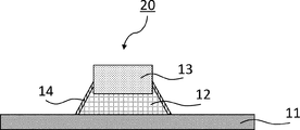
- FIG. 1 and 2 are cross-sectional views showing a schematic configuration of an embodiment of the electronic device of the present disclosure.
- a bonding layer 2 is provided on a substrate 1, and an electronic component 3 is provided on the bonding layer 2.
- a coating film 4 is formed so as to cover the side surface of the bonding layer 2.
- the bonding layer 12 may have a fillet protruding laterally from the side end of the electronic component 13, and when the bonding layer 12 has a fillet, the coating film 14 has the bonding. It is formed so as to cover the fillet of the layer 12.
- the bonding layer is a layer for bonding a substrate and an electronic component, and contains copper having a crystal grain size of 50 nm or less, which is more than 0% by mass and 60% by mass or less. If copper having a crystal grain size of 50 nm or less contained in the bonding layer is 0% by mass, the sinterability may be inferior. On the other hand, if the amount of copper having a crystal grain size of 50 nm or less contained in the bonding layer exceeds 60% by mass, the sulfur resistance of the obtained electronic device may decrease. From this point of view, the bonding layer may contain 5 to 55% by mass of copper having a crystal grain size of 50 nm or less.
- the content of copper having a crystal grain size of 50 nm or less contained in the bonding layer can be adjusted by appropriately adjusting the firing temperature and firing time of the bonding layer.
- the content of copper having a crystal grain size of 50 nm or less contained in the bonding layer can be measured by an electron backscatter diffraction pattern (EBSD) and calculated from the obtained crystal grain size distribution. It can be measured, specifically, by the method described in Examples.
- EBSD electron backscatter diffraction pattern
- the bonding layer may contain copper having a crystal grain size of more than 50 nm in an amount of 40% by mass or more and less than 100% by mass, or 45 to 95% by mass.
- the bonding layer contains copper having a crystal grain size of more than 50 nm within the above range, an electronic device having excellent sulfur resistance can be obtained.
- the upper limit of the crystal grain size of copper may be 1000 nm or 500 nm.
- the thickness of the bonding layer may be 5 to 100 ⁇ m, 10 to 80 ⁇ m, or 30 to 50 ⁇ m from the viewpoint of bonding reliability and thermal resistance.
- the coating contains at least one compound selected from copper (I) (Cu 2 O) and copper (II) oxide (Cu O).
- the coating film contains at least one compound selected from Cu 2 O and Cu O, the invasion of sulfur into the bonding layer can be suppressed and the generation of copper sulfide can be suppressed.
- the thickness of the film is Anm and the proportion of copper (I) (Cu 2 O) oxide in the copper oxide contained in the film is B mass%
- the following formula (1) is used from the viewpoint of enhancing sulfur resistance.
- the following formula (2) it is possible to obtain an electronic device having excellent resistance by the sulfur gas (S 8 ) test, which has stricter conditions than the conventional sulfur gas test. it can.
- the thickness of the coating film When the thickness (average value) of the coating film is 10 nm or more, the invasion of sulfur into the bonding layer is suppressed, and the generation of copper sulfide can be suppressed. From this point of view, the thickness of the coating film may be 30 nm or more, or 50 nm or more. On the other hand, the upper limit of the thickness of the coating film may be 2000 nm, 1000 nm, or 500 nm from the viewpoint of thermal resistance.
- the thickness of the coating film can be adjusted by appropriately adjusting the oxidation temperature and oxidation time of the coating film.
- the thickness of the coating film can be measured by using a field emission scanning electron microscope (FE-SEM) and an energy dispersive X-ray analysis (EDX), and specifically, by the method described in Examples. Can be measured.
- FE-SEM field emission scanning electron microscope
- EDX energy dispersive X-ray analysis
- the proportion of Cu 2 O present in the copper oxide contained in the coating film is 20% by mass or more, the sulfur resistance of the obtained electronic device can be enhanced. From this point of view, the proportion of Cu 2 O present in the copper oxide contained in the coating film may be 25% by mass or more, 60% by mass or more, or 75% by mass or more. It may be 100% by mass.
- the proportion of Cu 2 O present in the copper oxide contained in the coating film can be adjusted by appropriately adjusting the oxidation temperature and oxidation time of the coating film.
- the ratio of copper (I) oxide (Cu 2 O) can be measured by an X-ray diffraction (XRD) apparatus, and specifically, it can be measured by the method described in Examples.
- the proportion of copper (II) oxide (CuO) present in the coating film may be 0 to 80% by mass, 0 to 75% by mass, or 0 to 40% by mass. It may be 0 to 25% by mass.
- the proportion of copper (II) oxide (CuO) can be measured by an X-ray diffraction (XRD) apparatus.
- the total amount of copper oxide contained in the coating film may be 40 to 100% by mass, 60 to 100% by mass, or 80 to 100% by mass.
- substrate examples of the substrate include substrates made of materials such as copper, copper-plated copper, PPF (preplating lead frame), glass epoxy, and ceramics.
- Examples of electronic components include semiconductor elements, heat generating members, heat radiating members, and the like.
- Examples of the semiconductor element include an optical semiconductor element (light emitting element) such as an LED, a transistor, a diode, and the like, and may be an optical semiconductor element.
- the type of the optical semiconductor element is not particularly limited, and examples thereof include those in which a nitride semiconductor such as InN, AlN, GaN, InGaN, AlGaN, and InGaAlN is formed as a light emitting layer on a substrate by the MOBVC method or the like. ..
- the heat generating member may be the semiconductor element or a member having the semiconductor element, or may be another heat generating member. Examples of the heat generating member other than the semiconductor element include an optical pickup and a power transistor. Further, examples of the heat radiating member include a heat sink and a heat spreader.
- the electronic device of the present disclosure has excellent sulfur resistance, it is suitably used for in-vehicle lamps, street lights, and the like.
- a substrate on which electronic components are arranged on a copper paste is fired at 125 to 250 ° C. for 30 minutes to 10 hours in a reducing atmosphere to obtain the substrate and the electronic components.
- the firing process of joining via a bonding layer containing copper The substrate is heated at 150 to 250 ° C. for 3 minutes to 10 hours in an oxygen-containing atmosphere to oxidize the sides of the bonding layer to obtain copper (I) (Cu 2 O) and copper (II) oxide (II) oxide. It has an oxidation step of forming a film containing at least one compound selected from CuO).
- a copper paste is applied on a substrate, and electronic components are arranged on the copper paste.
- the substrate and electronic components those described in the above section ⁇ Electronic device> can be used.
- the copper paste is not particularly limited as long as it contains copper particles, but may include copper particles, large particle size copper particles having a particle size larger than the copper particles, and an organic solvent.
- the average particle size of the copper particles may be 1 to 1000 nm, 20 to 800 nm, or 30 to 500 nm from the viewpoint of the denseness of the bonding layer.
- the average value is an arithmetic mean value, and 10 or more copper particles may be used in the calculation.
- Copper particles can be obtained, for example, by reducing a copper compound with a reducing compound in the presence of a carboxylic acid amine salt. Further, the copper compound, the carboxylic acid amine salt, and the reducing compound may be mixed in an organic solvent.
- the heating temperature in the above mixing is a temperature at which the copper compound can be thermally decomposed and reduced to form copper particles, and may be, for example, 70 to 150 ° C. or 80 to 120 ° C.
- the copper compound is not particularly limited as long as it contains a copper atom, and examples thereof include copper carboxylate, copper oxide, copper hydroxide, and copper nitride.
- the copper compound may be copper carboxylate from the viewpoint of uniformity during the reaction. These may be used alone or in combination of two or more.
- copper carboxylate examples include copper formate (I), cupric acetate (I), copper propionate (I), copper butyrate (I), copper valerate (I), copper caproate (I), and copper caproate (I). ), Copper caproate (I), copper formate (II), cupric acetate (II), copper propionate (II), copper butyrate (II), copper valerate (II), copper caproate (II), capric acid Examples thereof include carboxylic acid copper anhydrides or hydrates such as copper (II), copper (II) caproate and copper (II) citrate.
- the copper carboxylate may be copper (II) acetate monohydrate from the viewpoint of productivity and availability. Further, these may be used alone or in combination of two or more.
- the carboxylic acid amine salt can be obtained from a carboxylic acid compound and an amine compound, and a commercially available product may be used, or a product obtained by synthesis in advance may be used. Further, the carboxylic acid compound and the amine compound may be separately charged into the reaction vessel in the process of producing the copper particles and produced in-situ.
- the carboxylic acid amine salt is produced by blending a carboxylic acid compound and an amine compound in an organic solvent in equal amounts of functional groups and mixing them under relatively mild temperature conditions of room temperature (25 ° C.) to about 100 ° C. ..
- the carboxylic acid amine salt may be taken out from the reaction solution containing the carboxylic acid amine salt by a distillation method, a recrystallization method or the like.
- the carboxylic acid compound constituting the carboxylic acid amine salt is not particularly limited as long as it is a compound having a carboxy group, and examples thereof include monocarboxylic acid, dicarboxylic acid, aromatic carboxylic acid, and hydroxy acid. These may be used alone or in combination of two or more.
- the amine compound constituting the carboxylic acid amine salt is not particularly limited as long as it is a compound having an amino group, and examples thereof include alkylmonoamine, alkyldiamine, and alkanolamine. These may be used alone or in combination of two or more.
- the reducing compound is not particularly limited as long as it has a reducing power for reducing the copper compound and liberating metallic copper.
- the reducing compound typically includes a hydrazine derivative.
- the hydrazine derivative include hydrazine monohydrate, methylhydrazine, ethylhydrazine, n-propylhydrazine, i-propylhydrazine, n-butylhydrazine, i-butylhydrazine, sec-butylhydrazine, t-butylhydrazine, n.
- -Pentylhydrazine i-pentylhydrazine, neo-pentylhydrazine, t-pentylhydrazine, n-hexylhydrazine, i-hexylhydrazine, n-heptylhydrazine, n-octylhydrazine, n-nonylhydrazine, n-decylhydrazine, n -Undecyl hydrazine, n-dodecyl hydrazine, cyclohexyl hydrazine, phenyl hydrazine, 4-methylphenyl hydrazine, benzyl hydrazine, 2-phenylethyl hydrazine, 2-hydrazine ethanol, acetohydrazine and the like can be mentioned. These may be used alone or in combination of two or more.
- the organic solvent used for producing the copper particles is not particularly limited as long as it can be used as a reaction solvent that does not impair the properties of the complex or the like formed from the mixture obtained by mixing the above-mentioned raw materials. it can.
- As the organic solvent an alcohol showing compatibility with the reducing compound may be used.
- Examples of the alcohol include 1-propanol, 2-propanol, butanol, pentanol, hexanol, heptanol, octanol, ethylene glycol, 1,3-propanediol, 1,2-propanediol, butyl carbitol, butyl carbitol acetate, and the like.
- Examples thereof include ethyl carbitol, ethyl carbitol acetate, diethylene glycol diethyl ether, and butyl cellosolve. These may be used alone or in combination of two or more.
- the amount of the copper compound, the carboxylic acid amine salt, and the reducing compound used may be 0.1 to 10 mol of the carboxylic acid amine salt and 0.5 to 5 mol of the reducing compound with respect to 1 mol of the copper compound, and the carboxylic acid amine salt may be used. It may be 1 to 5 mol and 0.5 to 3 mol of the reducing compound.
- the amount of the organic solvent may be such that each of the above components can sufficiently react, and for example, about 50 to 2000 mL may be used.
- the large particle size copper particles may have an average particle diameter of more than 1 ⁇ m and 30 ⁇ m or less, or 1 to 20 ⁇ m.
- the shape is not particularly limited, and spherical, plate-shaped, flake-shaped, scaly-shaped, dendritic-shaped, rod-shaped, wire-shaped, and the like can be used.
- the average particle size of the large particle size copper particles can be measured by using a laser diffraction / scattering type particle size distribution measuring device or the like.
- the large particle size copper particles may be those treated with a lubricant or a rust preventive.
- a typical such treatment is a treatment with a carboxylic acid compound.
- the carboxylic acid compound include formic acid, acetic acid, propionic acid, butyric acid, valeric acid, caproic acid, capric acid, octyl acid, nonanoic acid, capric acid, palmitic acid, oleic acid, stearic acid, isostearic acid and oxalic acid.
- Maronic acid succinic acid, glutaric acid, adipic acid, pimelli acid, suberic acid, azelaic acid, sebacic acid, diglycolic acid, benzoic acid, phthalic acid, isophthalic acid, terephthalic acid, salicylic acid, gallic acid, glycolic acid, lactic acid, Examples thereof include tartronic acid, malic acid, glyceric acid, hydroxybutyric acid, tartrate acid, citric acid and isocitrate.
- Organic solvent a known solvent can be used as long as it is a solvent that functions as a reducing agent.
- the organic solvent may be an alcohol, and examples thereof include an aliphatic polyhydric alcohol.
- examples of the aliphatic polyhydric alcohol include glycols such as ethylene glycol, diethylene glycol, propylene glycol, dipropylene glycol, 1,4-butanediol, glycerin, and polyethylene glycol. These organic solvents may be used alone or in combination of two or more.
- the blending amount may be 7 to 20 parts by mass when the copper particles are 100 parts by mass.
- the blending amount of the organic solvent is 7 parts by mass or more, the viscosity does not become too high and workability can be improved, and when it is 20 parts by mass or less, the decrease in viscosity is suppressed and the settlement of copper in the paste is prevented. It can be suppressed and reliability can be increased.
- the copper paste has low stress such as thermosetting resin, curing accelerator, rubber, silicone, etc., which are generally blended in this kind of composition, as long as the effects of the present disclosure are not impaired.
- Agents, coupling agents, antifoaming agents, surfactants, pigments, colorants such as dyes, various polymerization inhibitors, antioxidants and the like can be blended as needed.
- One of these components may be used alone, or two or more thereof may be mixed and used.
- the copper paste is sufficiently mixed with the above-mentioned copper particles, large particle size copper particles to be blended if necessary, an organic solvent, and the like, and then further kneaded with a disperser, a kneader, a three-roll mill, or the like. It can then be prepared by defoaming.
- the substrate on which the electronic components are arranged on the copper paste is fired at 125 to 250 ° C. for 30 minutes to 10 hours in a reducing atmosphere, and the substrate and the electronic components are bonded to each other via a bonding layer containing copper.
- the firing temperature is less than 125 ° C., a bonding failure may occur, and if it exceeds 250 ° C., the LED element may be damaged. From this point of view, the firing temperature may be 150 to 230 ° C. or 180 to 210 ° C.
- the firing time may be 1 to 4 hours or 1 to 3 hours.
- Examples of the reducing atmosphere include a hydrogen gas atmosphere, an inert gas such as argon and nitrogen, and / or a mixed gas atmosphere of nitrogen gas such as forming gas and hydrogen gas, and a formic acid atmosphere.
- the substrate is heated at 150 to 250 ° C. for 3 minutes to 10 hours in an oxygen-containing atmosphere to oxidize the sides of the bonding layer to obtain copper (I) oxide (Cu 2 O) and copper oxide.
- (II) A film containing at least one compound selected from (CuO) is formed. If the heating temperature (oxidation temperature) is less than 150 ° C., the film formation may be insufficient, and if it exceeds 250 ° C., the proportion of copper (II) oxide in the film may increase. From this point of view, the heating temperature may be 180 to 230 ° C. or 190 to 210 ° C.
- the heating time (oxidation time) is less than 3 minutes, the film formation may be insufficient, and if it exceeds 10 hours, the proportion of copper (II) oxide in the film may increase. From this point of view, the heating time may be 0.25 to 4 hours or 0.5 to 3 hours.
- Examples of the oxygen-containing atmosphere include an atmospheric atmosphere.
- hydrazine monohydrate as a reducing compound (manufactured by Fujifilm Wako Pure Chemical Industries, Ltd., trade name: hydrazine monohydrate) was added to 3 mL of 1-propanol. ) A solution in which 20 mmol was dissolved was added to the copper precursor solution in the sample bottle, and the mixture was stirred for 5 minutes.
- Example 1 Each component of the type and the blending amount shown in Table 1 was mixed and kneaded with a roll to obtain a bonding paste (copper paste).
- the copper paste was applied onto a substrate (manufactured by Creative Science Co., Ltd., trade name: aluminum substrate for REGAL) so that the thickness after firing was 30 ⁇ m, and electronic components (Nichia) were applied onto the copper paste. Nichia Corporation, trade name: NVSW119CT) was placed.
- the substrate on which the electronic components were arranged on the copper paste was fired at 200 ° C. for 1 hour in a forming gas atmosphere, and the substrate and the electronic components were bonded via a bonding layer containing copper.
- the substrate was heated at 250 ° C.
- the bonding layer has a fillet protruding laterally from the side end of the electronic component. It was confirmed that the coating film was formed so as to cover the fillet.
- Examples 2 to 7, Comparative Examples 1 and 2 Each component of the type and the blending amount shown in Table 1 was mixed and kneaded with a roll to obtain a bonding paste of each Example and Comparative Example. Using the obtained bonding paste, the electronic devices of the respective Examples and Comparative Examples were subjected to the methods described in Example 1 except that the firing temperature, firing time, heating temperature, and heating time were changed to those shown in Table 1. Obtained.
- -Copper particles Copper particles obtained in Synthesis Example 1 (average particle diameter 50 nm)
- -Silver particles Spherical silver particles (manufactured by Mitsuboshi Belting Co., Ltd., trade name: MDot, average particle diameter 50 nm)
- -Copper powder Cu-HWQ (manufactured by Fukuda Metal Foil Powder Industry Co., Ltd., trade name, average particle size 1.5 ⁇ m)
- -Silver powder AgC-212D (manufactured by Fukuda Metal Foil Powder Industry Co., Ltd., trade name, average particle diameter 5 ⁇ m)
- Organic solvent Diethylene glycol, manufactured by Tokyo Chemical Industry Co., Ltd.
- Vf forward voltage
- the electronic devices of Examples 1 to 7 in which the proportion of copper having a crystal particle size of 50 nm or less contained in the bonding layer is 60% by mass or less and having a coating film containing copper oxide covering the sides of the bonding layer are all sulfur resistant.
- the increase rate of Vf in the test A is less than 10%
- the increase rate of Vf in the sulfurization resistance test B is less than 20%, indicating that the sulfur resistance is excellent.
- the increase rate of Vf in the sulfurization resistance test A is less than 20%, but the sulfurization resistance test.
- the rate of increase in Vf in B was as high as 20% or more, and the sulfur resistance was inferior as compared with Examples. Further, in the electronic device of Comparative Example 2 in which the silver paste was used as the bonding paste, the rate of increase in Vf was as high as 20% or more in both the sulfurization resistance test A and the sulfurization resistance test B, and the sulfur resistance was higher than that of the examples. Was inferior.
Landscapes
- Engineering & Computer Science (AREA)
- General Engineering & Computer Science (AREA)
- Mechanical Engineering (AREA)
- Manufacturing & Machinery (AREA)
- Microelectronics & Electronic Packaging (AREA)
- Optics & Photonics (AREA)
- Physics & Mathematics (AREA)
- Chemical & Material Sciences (AREA)
- Composite Materials (AREA)
- Materials Engineering (AREA)
- Powder Metallurgy (AREA)
- Conductive Materials (AREA)
- Die Bonding (AREA)
- Chemical Kinetics & Catalysis (AREA)
- General Chemical & Material Sciences (AREA)
Abstract
Description
本開示は、かかる知見に基づいて完成したものである。
[1]基板と、前記基板上に設けられ、結晶粒径が50nm以下の銅を、0質量%を超え60質量%以下含む接合層と、前記接合層上に設けられた電子部品と、前記接合層の側方を覆い、酸化銅(I)(Cu2O)及び酸化銅(II)(CuO)から選ばれる少なくとも1種の化合物を含む被膜と、を有することを特徴とする電子装置。
[2]前記接合層は、前記電子部品の側端よりも側方に張り出したフィレットを有し、前記被膜は、前記フィレットを覆うことを特徴とする、上記[1]に記載の電子装置。
[3]前記被膜の厚さをAnm、前記被膜に含まれる酸化銅のうち酸化銅(I)(Cu2O)が存在する割合をB質量%とした時、下記式(1)の関係にあることを特徴とする上記[1]又は[2]に記載の電子装置。
A≧10 B≧20 (1)
[4]前記被膜の厚さをAnm、前記被膜に含まれる酸化銅のうち酸化銅(I)(Cu2O)が存在する割合をB質量%とした時、下記式(2)を満たすことを特徴とする上記[3]に記載の電子装置。
B≧1.15×A-0.2×100 (2)
[5]前記電子部品が、光半導体素子であることを特徴とする、上記[1]~[4]のいずれかに記載の電子装置。
[6]上記[1]~[5]のいずれかに記載の電子装置からなる車載用ランプ。
[7]上記[1]~[5]のいずれかに記載の電子装置からなる街路灯。
[8]電子部品が銅ペースト上に配置された基板を、125~250℃で30分~10時間、還元性雰囲気下で焼成し、前記基板と前記電子部品とを銅を含む接合層を介して接合する焼成工程と、前記基板を150~250℃で3分~10時間、酸素含有雰囲気下で加熱し、前記接合層の側方を酸化して、酸化銅(I)(Cu2O)及び酸化銅(II)(CuO)から選ばれる少なくとも1種の化合物を含む被膜を形成する酸化工程と、を有する電子装置の製造方法。
本実施形態の電子装置は、基板と、
前記基板上に設けられ、結晶粒径が50nm以下の銅を、0質量%を超え60質量%以下含む接合層と、
前記接合層上に設けられた電子部品と、
前記接合層の側方を覆い、酸化銅(I)(Cu2O)及び酸化銅(II)(CuO)から選ばれる少なくとも1種の化合物を含む被膜と、を有する。
接合層は、基板と電子部品とを接合する層であり、結晶粒径が50nm以下の銅を、0質量%を超え60質量%以下含む。接合層に含まれる結晶粒径50nm以下の銅が0質量%であると焼結性に劣るおそれがある。一方、接合層に含まれる結晶粒径50nm以下の銅が60質量%を超えると得られる電子装置の硫黄耐性が低下するおそれがある。このような観点から、接合層は、結晶粒径50nm以下の銅を5~55質量%含んでもよい。
上記接合層中に含まれる結晶粒径50nm以下の銅の含有量は、該接合層の焼成温度及び焼成時間を適宜調整することにより、調整することができる。
なお、上記接合層に含まれる結晶粒径が50nm以下の銅の含有量は、電子後方散乱回折法(EBSD: Electron Backscatter Diffraction Pattern)により測定し、得られた結晶粒径分布から算出することができ、具体的には実施例に記載の方法により測定することができる。
被膜は、酸化銅(I)(Cu2O)及び酸化銅(II)(CuO)から選ばれる少なくとも1種の化合物を含む。被膜がCu2O及びCuOから選ばれる少なくとも1種の化合物を含むことにより、接合層内部への硫黄の侵入が抑えられ、硫化銅の発生を抑制することができる。
A≧10 B≧20 (1)
B≧1.15×A-0.2×100 (2)
上記被膜の厚さは、該被膜の酸化温度及び酸化時間を適宜調整することにより、調整することができる。
なお、上記被膜の厚さは、電界放出型走査電子顕微鏡(FE-SEM)及びエネルギー分散型X線分析(EDX)を用いて測定することができ、具体的には実施例に記載の方法により測定することができる。
上記被膜に含まれる酸化銅のうちCu2Oが存在する割合は、該被膜の酸化温度及び酸化時間を適宜調整することにより、調整することができる。
なお、上記酸化銅(I)(Cu2O)の割合は、X線回折(XRD)装置により測定することができ、具体的には実施例に記載の方法により測定することができる。
上記酸化銅(II)(CuO)の割合は、X線回折(XRD)装置により測定することができる。
基板としては、例えば、銅、銅メッキ銅、PPF(プリプレーティングリードフレーム)、ガラスエポキシ、セラミックス等の材料で形成された基板が挙げられる。
電子部品としては、例えば、半導体素子、発熱部材、放熱部材等が挙げられる。
半導体素子としては、例えば、LED等の光半導体素子(発光素子)、トランジスタ、ダイオード等が挙げられ、光半導体素子であってもよい。
光半導体素子の種類は特に制限されるものではなく、例えば、MOBVC法等によって基板上にInN、AlN、GaN、InGaN、AlGaN、InGaAlN等の窒化物半導体を発光層として形成させたものも挙げられる。
発熱部材としては、上記半導体素子又は該半導体素子を有する部材でもよいし、それ以外の発熱部材でもよい。半導体素子以外の発熱部材としては、光ピックアップ、パワートランジスタ等が挙げられる。また、放熱部材としては、ヒートシンク、ヒートスプレッダー等が挙げられる。
本開示の電子装置の製造方法は、電子部品が銅ペースト上に配置された基板を、125~250℃で30分~10時間、還元性雰囲気下で焼成し、前記基板と前記電子部品とを銅を含む接合層を介して接合する焼成工程と、
前記基板を150~250℃で3分~10時間、酸素含有雰囲気下で加熱し、前記接合層の側方を酸化して、酸化銅(I)(Cu2O)及び酸化銅(II)(CuO)から選ばれる少なくとも1種の化合物を含む被膜を形成する酸化工程と、を有する。
本工程では、まず、基板上に銅ペーストを塗布し、該銅ペースト上に電子部品を配置する。
基板及び電子部品は、上記<電子装置>の項で説明したものを用いることができる。
銅ペーストとしては、銅粒子を含めば特に限定されないが、銅粒子、該銅粒子よりも粒径の大きい大粒径銅粒子、及び有機溶剤を含んでもよい。
銅粒子の平均粒子径は、接合層の緻密性の観点から、1~1000nmであってもよく、20~800nmであってもよく、は30~500nmであってもよい。
なお、上記銅粒子の平均粒子径は、走査電子顕微鏡(例えば、日本電子(株)製、商品名:JSM-7600F;SEM)の観察画像に基づく任意に選択した10個の銅粒子(n=10)の平均値として算出する。なお、平均値は算術平均値であり、その算出にあたっては10個以上の銅粒子を用いてもよい。
銅粒子は、例えば、銅化合物を、カルボン酸アミン塩存在下、還元性化合物によって還元することにより得ることができる。また、銅化合物、カルボン酸アミン塩、及び還元性化合物の混合は、有機溶剤中で行ってもよい。
上記混合における加熱温度は、銅化合物が熱分解及び還元され、銅粒子が生成できる温度であり、例えば、70~150℃であってもよく、80~120℃であってもよい。
還元性化合物としては、典型的には、ヒドラジン誘導体が挙げられる。ヒドラジン誘導体としては、例えば、ヒドラジン一水和物、メチルヒドラジン、エチルヒドラジン、n-プロピルヒドラジン、i-プロピルヒドラジン、n-ブチルヒドラジン、i-ブチルヒドラジン、sec-ブチルヒドラジン、t-ブチルヒドラジン、n-ペンチルヒドラジン、i-ペンチルヒドラジン、neo-ペンチルヒドラジン、t-ペンチルヒドラジン、n-ヘキシルヒドラジン、i-ヘキシルヒドラジン、n-ヘプチルヒドラジン、n-オクチルヒドラジン、n-ノニルヒドラジン、n-デシルヒドラジン、n-ウンデシルヒドラジン、n-ドデシルヒドラジン、シクロヘキシルヒドラジン、フェニルヒドラジン、4-メチルフェニルヒドラジン、ベンジルヒドラジン、2-フェニルエチルヒドラジン、2-ヒドラジノエタノール、アセトヒドラジン等が挙げられる。これらは単独で用いてもよく、2種以上を併用してもよい。
有機溶剤は上記各成分が十分に反応を行うことができる量であればよく、例えば、50~2000mL程度用いるようにすればよい。
大粒径銅粒子は、平均粒子径が1μmよりも大きく30μm以下であってもよく、1~20μmであってもよい。また、形状は特に限定されず、球状、プレート型、フレーク状、鱗片状、樹枝状、ロッド状、ワイヤー状等が使用できる。
なお、上記大粒径銅粒子の平均粒子径は、レーザー回折散乱式粒度分布測定装置等を用いて測定することができる。
有機溶剤は、還元剤として機能する溶剤であれば公知の溶剤を用いることができる。
上記有機溶剤としては、アルコールであってもよく、例えば、脂肪族多価アルコールを挙げることができる。脂肪族多価アルコールとしては、例えば、エチレングリコール、ジエチレングリコール、プロピレングリコール、ジプロビレングリコール、1,4-ブタンジオール、グリセリン、ポリエチレングリコールなどのグリコール類などを挙げることができる。これらの有機溶剤は、単独で用いてもよく、2種以上を併用してもよい。
上記焼成温度が125℃未満であると接合不良を起こすおそれがあり、250℃を超えるとLED素子を損傷するおそれがある。このような観点から、焼成温度は150~230℃であってもよく、180~210℃であってもよい。
本工程では、前記基板を150~250℃で3分~10時間、酸素含有雰囲気下で加熱し、前記接合層の側方を酸化して、酸化銅(I)(Cu2O)及び酸化銅(II)(CuO)から選ばれる少なくとも1種の化合物を含む被膜を形成する。
上記加熱温度(酸化温度)が150℃未満であると被膜形成が不足するおそれがあり、250℃を超えると被膜中の酸化銅(II)の割合が増加するおそれがある。このような観点から、加熱温度は180~230℃であってもよく、190~210℃であってもよい。
カルボン酸化合物としてノナン酸(東京化成工業(株)製、商品名:ノナン酸)40mmolと、アミン化合物としてヘキシルアミン(東京化成工業(株)製、商品名:ヘキシルアミン)40mmolを、50mLのサンプルビンに入れ、アルミブロック式加熱撹拌機中、撹拌・混合すると、60℃まで発熱した。続けて60℃で15分間撹拌・混合し、室温(25℃)まで冷却することで、ノナン酸ヘキシルアミン塩(収量10.3g、収率99.2%)を得た。
銅化合物として酢酸銅(II)一水和物(東京化成工業(株)製、商品名:酢酸銅(II)一水和物)20mmolと、カルボン酸アミン塩として調製例1で得たノナン酸ヘキシルアミン塩40mmolと、有機溶剤としてブチルセロソルブ(東京化成工業(株)製)3mLとを50mLのサンプルビンに入れ、アルミブロック式加熱撹拌機中、90℃で5分間混合し、銅前駆体溶液とした。該銅前駆体溶液を室温(25℃)まで冷却した後、1-プロパノール3mLに、還元性化合物としてヒドラジン一水和物(富士フイルム和光純薬(株)製、商品名:ヒドラジン一水和物)20mmolを溶解させた溶液を、サンプルビンの銅前駆体溶液に加え、5分間撹拌した。
なお、上記銅粒子の平均粒子径は、走査電子顕微鏡(日本電子(株)製、商品名:JSM-7600F;SEM)の観察画像に基づく任意に選択した10個の銅粒子(n=10)の平均値として算出した。
表1に記載の種類及び配合量の各成分を混合し、ロールで混練し、接合用ペースト(銅ペースト)を得た。
次に、基板(創造科学(有)製、商品名:REGAL用アルミ基板)上に上記銅ペーストを焼成後の厚さが30μmとなるように塗布し、該銅ペースト上に電子部品(日亜化学工業(株)製、商品名:NVSW119CT)を配置した。次いで、電子部品が銅ペースト上に配置された基板を、200℃で1時間、フォーミングガス雰囲気下で焼成し、上記基板と上記電子部品とを銅を含む接合層を介して接合した。次に、上記基板を大気雰囲気下で、250℃で5分間加熱し、上記接合層の側方を酸化して、酸化銅を含む被膜を形成することにより実施例1の電子装置を得た。
なお、得られた電子装置について走査電子顕微鏡(日本電子(株)製、商品名:JSM-7600F;SEM)観察により、上記接合層は上記電子部品の側端よりも側方に張り出したフィレットを有し、上記被膜は該フィレットを覆うように形成されていることを確認した。
表1に記載の種類及び配合量の各成分を混合し、ロールで混練し、各実施例及び比較例の接合用ペーストを得た。得られた接合用ペーストを用い、表1に記載の焼成温度、焼成時間、加熱温度、加熱時間に変更したこと以外は実施例1に記載の方法により、各実施例及び比較例の電子装置を得た。
・銅粒子:合成例1で得られた銅粒子(平均粒子径50nm)
・銀粒子:球状銀粒子(三ツ星ベルト(株)製、商品名:MDot、平均粒子径50nm)
・銅粉:Cu-HWQ(福田金属箔粉工業(株)製、商品名、平均粒子径1.5μm)
・銀粉:AgC-212D(福田金属箔粉工業(株)製、商品名、平均粒子径5μm)
・有機溶剤:ジエチレングリコール、東京化成工業(株)製
<電子装置の評価方法>
(1)接合層に含まれる結晶粒径50nm以下の銅の割合
電子装置をエポキシ樹脂で包埋した後、接合層断面を研削・研磨・CP加工によって露出させ、接合層の断面を電界放出型走査顕微鏡((株)日立ハイテクノロジーズ製、商品名:SU5000)による電子後方散乱回折法で粒径解析し、結晶粒径のヒストグラムを出力した。得られたヒストグラムより結晶粒径50nm以下の割合を算出した。
電子装置をエポキシ樹脂で包埋した後、接合層断面を研削・研磨・CP加工によって露出させ、電界放出型走査顕微鏡((株)日立ハイテクノロジーズ製、商品名:SU5000)によるエネルギー分散型X線分析で被膜近傍を線分析し、酸素原子が検出された距離を被膜厚とした。
電子装置のフィレット部をX線回折装置((株)リガク製、商品名:SmartLab SE)の超微小分析を行い、リートベルト法によって酸化銅(I)、酸化銅(II)の定量値を算出した。
JIS C 60068-2-60:2018の4種混合ガス試験に準拠し、電子装置を混合ガス(H2S:10ppb、NO2:200ppb、Cl2:10ppb、SO2:100ppb)下で、40℃、90%RH、336時間処理した後、順方向電圧(Vf)を測定し初期値からの変化率(上昇率)を求め、下記基準により評価した。
A:Vfの上昇率が10%未満
B:Vfの上昇率が10%以上20%未満
C:Vfの上昇率が20%以上
硫黄粉末1gを入れたガラス容器内に電子装置を入れ、ガラス容器を100℃のオイルバスに浸漬し、900時間保持した後、順方向電圧(Vf)を測定し初期値からの変化率(上昇率)を求め、下記基準により評価した。
A:Vfの上昇率が10%未満
B:Vfの上昇率が10%以上20%未満
C:Vfの上昇率が20%以上

1,11 基板
2,12 接合層
3,13 電子部品
4,14 被膜
Claims (8)
- 基板と、
前記基板上に設けられ、結晶粒径が50nm以下の銅を、0質量%を超え60質量%以下含む接合層と、
前記接合層上に設けられた電子部品と、
前記接合層の側方を覆い、酸化銅(I)(Cu2O)及び酸化銅(II)(CuO)から選ばれる少なくとも1種の化合物を含む被膜と、
を有することを特徴とする電子装置。 - 前記接合層は、前記電子部品の側端よりも側方に張り出したフィレットを有し、前記被膜は、前記フィレットを覆うことを特徴とする、請求項1に記載の電子装置。
- 前記被膜の厚さをAnm、前記被膜に含まれる酸化銅のうち酸化銅(I)(Cu2O)が存在する割合をB質量%とした時、下記式(1)の関係にあることを特徴とする請求項1又は2に記載の電子装置。
A≧10 B≧20 (1) - 前記被膜の厚さをAnm、前記被膜に含まれる酸化銅のうち酸化銅(I)(Cu2O)が存在する割合をB質量%とした時、下記式(2)を満たすことを特徴とする請求項3に記載の電子装置。
B≧1.15×A-0.2×100 (2) - 前記電子部品が、光半導体素子であることを特徴とする、請求項1~4のいずれか1項に記載の電子装置。
- 請求項1~5のいずれか1項に記載の電子装置からなる車載用ランプ。
- 請求項1~5のいずれか1項に記載の電子装置からなる街路灯。
- 電子部品が銅ペースト上に配置された基板を、125~250℃で30分~10時間、還元性雰囲気下で焼成し、前記基板と前記電子部品とを銅を含む接合層を介して接合する焼成工程と、
前記基板を150~250℃で3分~10時間、酸素含有雰囲気下で加熱し、前記接合層の側方を酸化して、酸化銅(I)(Cu2O)及び酸化銅(II)(CuO)から選ばれる少なくとも1種の化合物を含む被膜を形成する酸化工程と、
を有する電子装置の製造方法。
Priority Applications (5)
| Application Number | Priority Date | Filing Date | Title |
|---|---|---|---|
| EP20832264.4A EP3991880A4 (en) | 2019-06-27 | 2020-06-10 | Electronic device and method for manufacturing electronic device |
| US17/622,256 US12087721B2 (en) | 2019-06-27 | 2020-06-10 | Electronic device and method for manufacturing electronic device |
| KR1020217042160A KR102610553B1 (ko) | 2019-06-27 | 2020-06-10 | 전자 장치 및 전자 장치의 제조 방법 |
| JP2021528136A JP7231734B2 (ja) | 2019-06-27 | 2020-06-10 | 電子装置及び電子装置の製造方法 |
| CN202080046134.0A CN114072905A (zh) | 2019-06-27 | 2020-06-10 | 电子装置以及电子装置的制造方法 |
Applications Claiming Priority (2)
| Application Number | Priority Date | Filing Date | Title |
|---|---|---|---|
| JP2019120133 | 2019-06-27 | ||
| JP2019-120133 | 2019-06-27 |
Publications (1)
| Publication Number | Publication Date |
|---|---|
| WO2020261993A1 true WO2020261993A1 (ja) | 2020-12-30 |
Family
ID=74061921
Family Applications (1)
| Application Number | Title | Priority Date | Filing Date |
|---|---|---|---|
| PCT/JP2020/022837 Ceased WO2020261993A1 (ja) | 2019-06-27 | 2020-06-10 | 電子装置及び電子装置の製造方法 |
Country Status (6)
| Country | Link |
|---|---|
| US (1) | US12087721B2 (ja) |
| EP (1) | EP3991880A4 (ja) |
| JP (1) | JP7231734B2 (ja) |
| KR (1) | KR102610553B1 (ja) |
| CN (1) | CN114072905A (ja) |
| WO (1) | WO2020261993A1 (ja) |
Cited By (1)
| Publication number | Priority date | Publication date | Assignee | Title |
|---|---|---|---|---|
| WO2025057964A1 (ja) | 2023-09-11 | 2025-03-20 | アピックヤマダ株式会社 | 実装装置及び実装方法 |
Families Citing this family (1)
| Publication number | Priority date | Publication date | Assignee | Title |
|---|---|---|---|---|
| CN116601750A (zh) * | 2020-12-16 | 2023-08-15 | 香港大学 | 半导体工业中用于封装应用的cu-cu直接焊接 |
Citations (6)
| Publication number | Priority date | Publication date | Assignee | Title |
|---|---|---|---|---|
| JP2007067452A (ja) | 2006-12-11 | 2007-03-15 | Sharp Corp | 半導体発光装置 |
| JP2014054653A (ja) | 2012-09-12 | 2014-03-27 | Mitsubishi Materials Corp | Au−Sn合金含有ペースト、Au−Sn合金薄膜及びその成膜方法 |
| WO2014156638A1 (ja) * | 2013-03-26 | 2014-10-02 | 古河電気工業株式会社 | 全固体二次電池 |
| JP2016219256A (ja) * | 2015-05-20 | 2016-12-22 | 住友金属鉱山株式会社 | Cuペースト組成物および厚膜導体 |
| JP2017075334A (ja) | 2012-03-05 | 2017-04-20 | ナミックス株式会社 | 熱伝導性ペースト及びその使用 |
| JP2018029143A (ja) * | 2016-08-18 | 2018-02-22 | 古河電気工業株式会社 | 半導体デバイス及びその製造方法 |
Family Cites Families (7)
| Publication number | Priority date | Publication date | Assignee | Title |
|---|---|---|---|---|
| JP2005057134A (ja) * | 2003-08-06 | 2005-03-03 | Fujikura Ltd | 電子部品およびその製造方法 |
| JP5123633B2 (ja) * | 2007-10-10 | 2013-01-23 | ルネサスエレクトロニクス株式会社 | 半導体装置および接続材料 |
| CN102143654A (zh) * | 2010-01-29 | 2011-08-03 | 旭硝子株式会社 | 元件搭载用基板及其制造方法 |
| JP6622971B2 (ja) * | 2015-02-24 | 2019-12-18 | 古河電気工業株式会社 | 加熱接合材料、接合構造体、並びに加熱接合材料の製造方法及び該加熱接合材料を用いた接合方法 |
| EP3758048B1 (en) * | 2015-10-02 | 2022-11-09 | Mitsui Mining & Smelting Co., Ltd. | A bonding junction structure |
| JP6693642B2 (ja) * | 2016-09-29 | 2020-05-13 | 大口マテリアル株式会社 | リードフレーム |
| JP6526889B1 (ja) * | 2018-08-01 | 2019-06-05 | Jx金属株式会社 | セラミックス層と銅粉ペースト焼結体の積層体 |
-
2020
- 2020-06-10 JP JP2021528136A patent/JP7231734B2/ja active Active
- 2020-06-10 WO PCT/JP2020/022837 patent/WO2020261993A1/ja not_active Ceased
- 2020-06-10 KR KR1020217042160A patent/KR102610553B1/ko active Active
- 2020-06-10 EP EP20832264.4A patent/EP3991880A4/en active Pending
- 2020-06-10 US US17/622,256 patent/US12087721B2/en active Active
- 2020-06-10 CN CN202080046134.0A patent/CN114072905A/zh active Pending
Patent Citations (6)
| Publication number | Priority date | Publication date | Assignee | Title |
|---|---|---|---|---|
| JP2007067452A (ja) | 2006-12-11 | 2007-03-15 | Sharp Corp | 半導体発光装置 |
| JP2017075334A (ja) | 2012-03-05 | 2017-04-20 | ナミックス株式会社 | 熱伝導性ペースト及びその使用 |
| JP2014054653A (ja) | 2012-09-12 | 2014-03-27 | Mitsubishi Materials Corp | Au−Sn合金含有ペースト、Au−Sn合金薄膜及びその成膜方法 |
| WO2014156638A1 (ja) * | 2013-03-26 | 2014-10-02 | 古河電気工業株式会社 | 全固体二次電池 |
| JP2016219256A (ja) * | 2015-05-20 | 2016-12-22 | 住友金属鉱山株式会社 | Cuペースト組成物および厚膜導体 |
| JP2018029143A (ja) * | 2016-08-18 | 2018-02-22 | 古河電気工業株式会社 | 半導体デバイス及びその製造方法 |
Non-Patent Citations (1)
| Title |
|---|
| See also references of EP3991880A4 |
Cited By (1)
| Publication number | Priority date | Publication date | Assignee | Title |
|---|---|---|---|---|
| WO2025057964A1 (ja) | 2023-09-11 | 2025-03-20 | アピックヤマダ株式会社 | 実装装置及び実装方法 |
Also Published As
| Publication number | Publication date |
|---|---|
| KR20220013397A (ko) | 2022-02-04 |
| US20220254748A1 (en) | 2022-08-11 |
| US12087721B2 (en) | 2024-09-10 |
| CN114072905A (zh) | 2022-02-18 |
| EP3991880A4 (en) | 2023-07-26 |
| EP3991880A1 (en) | 2022-05-04 |
| JPWO2020261993A1 (ja) | 2020-12-30 |
| JP7231734B2 (ja) | 2023-03-01 |
| KR102610553B1 (ko) | 2023-12-08 |
Similar Documents
| Publication | Publication Date | Title |
|---|---|---|
| TWI693266B (zh) | 糊料組合物、半導體裝置及電氣‧電子零件 | |
| EP4501495A1 (en) | Oxide-containing plate-like copper particles, paste composition, semiconductor device, electrical component and electronic component | |
| CN113165069B (zh) | 铜粒子、铜粒子的制造方法、铜膏和半导体装置以及电气/电子部件 | |
| JP7231734B2 (ja) | 電子装置及び電子装置の製造方法 | |
| JP7731972B2 (ja) | ペースト組成物、半導体装置、電気部品及び電子部品 | |
| JP2022026615A (ja) | 被覆銅粒子、被覆銅粒子の製造方法、銅ペースト、銅ペーストの製造方法、及び半導体装置 | |
| JP2021102808A (ja) | 接合材、及び物品 | |
| WO2016080544A1 (ja) | 金属表面の処理方法並びに当該方法により処理された銀被着銅及び複合金属体 | |
| TWI699412B (zh) | 糊料組合物、半導體裝置及電氣‧電子零件 | |
| CN118891118A (zh) | 含氧化物的板状铜粒子、膏组合物、半导体装置、电气部件和电子部件 | |
| CN118871229A (zh) | 铜粒子及其制造方法、膏组合物、半导体装置、电气部件和电子部件 | |
| JP6938125B2 (ja) | 接合体およびその製造方法、並びに半導体モジュール | |
| JP2021134362A (ja) | 被覆銅粒子、銅ペースト及び半導体装置 |
Legal Events
| Date | Code | Title | Description |
|---|---|---|---|
| 121 | Ep: the epo has been informed by wipo that ep was designated in this application |
Ref document number: 20832264 Country of ref document: EP Kind code of ref document: A1 |
|
| ENP | Entry into the national phase |
Ref document number: 20217042160 Country of ref document: KR Kind code of ref document: A Ref document number: 2021528136 Country of ref document: JP Kind code of ref document: A |
|
| NENP | Non-entry into the national phase |
Ref country code: DE |
|
| WWE | Wipo information: entry into national phase |
Ref document number: 2020832264 Country of ref document: EP |
|
| ENP | Entry into the national phase |
Ref document number: 2020832264 Country of ref document: EP Effective date: 20220127 |