WO2021020064A1 - 積層体およびその製造方法 - Google Patents
積層体およびその製造方法 Download PDFInfo
- Publication number
- WO2021020064A1 WO2021020064A1 PCT/JP2020/026840 JP2020026840W WO2021020064A1 WO 2021020064 A1 WO2021020064 A1 WO 2021020064A1 JP 2020026840 W JP2020026840 W JP 2020026840W WO 2021020064 A1 WO2021020064 A1 WO 2021020064A1
- Authority
- WO
- WIPO (PCT)
- Prior art keywords
- nickel
- film layer
- plating film
- mass
- laminate according
- Prior art date
- Legal status (The legal status is an assumption and is not a legal conclusion. Google has not performed a legal analysis and makes no representation as to the accuracy of the status listed.)
- Ceased
Links
Images

Classifications
-
- C—CHEMISTRY; METALLURGY
- C23—COATING METALLIC MATERIAL; COATING MATERIAL WITH METALLIC MATERIAL; CHEMICAL SURFACE TREATMENT; DIFFUSION TREATMENT OF METALLIC MATERIAL; COATING BY VACUUM EVAPORATION, BY SPUTTERING, BY ION IMPLANTATION OR BY CHEMICAL VAPOUR DEPOSITION, IN GENERAL; INHIBITING CORROSION OF METALLIC MATERIAL OR INCRUSTATION IN GENERAL
- C23C—COATING METALLIC MATERIAL; COATING MATERIAL WITH METALLIC MATERIAL; SURFACE TREATMENT OF METALLIC MATERIAL BY DIFFUSION INTO THE SURFACE, BY CHEMICAL CONVERSION OR SUBSTITUTION; COATING BY VACUUM EVAPORATION, BY SPUTTERING, BY ION IMPLANTATION OR BY CHEMICAL VAPOUR DEPOSITION, IN GENERAL
- C23C28/00—Coating for obtaining at least two superposed coatings either by methods not provided for in a single one of groups C23C2/00 - C23C26/00 or by combinations of methods provided for in subclasses C23C and C25C or C25D
- C23C28/30—Coatings combining at least one metallic layer and at least one inorganic non-metallic layer
- C23C28/32—Coatings combining at least one metallic layer and at least one inorganic non-metallic layer including at least one pure metallic layer
- C23C28/322—Coatings combining at least one metallic layer and at least one inorganic non-metallic layer including at least one pure metallic layer only coatings of metal elements only
-
- C—CHEMISTRY; METALLURGY
- C23—COATING METALLIC MATERIAL; COATING MATERIAL WITH METALLIC MATERIAL; CHEMICAL SURFACE TREATMENT; DIFFUSION TREATMENT OF METALLIC MATERIAL; COATING BY VACUUM EVAPORATION, BY SPUTTERING, BY ION IMPLANTATION OR BY CHEMICAL VAPOUR DEPOSITION, IN GENERAL; INHIBITING CORROSION OF METALLIC MATERIAL OR INCRUSTATION IN GENERAL
- C23C—COATING METALLIC MATERIAL; COATING MATERIAL WITH METALLIC MATERIAL; SURFACE TREATMENT OF METALLIC MATERIAL BY DIFFUSION INTO THE SURFACE, BY CHEMICAL CONVERSION OR SUBSTITUTION; COATING BY VACUUM EVAPORATION, BY SPUTTERING, BY ION IMPLANTATION OR BY CHEMICAL VAPOUR DEPOSITION, IN GENERAL
- C23C18/00—Chemical coating by decomposition of either liquid compounds or solutions of the coating forming compounds, without leaving reaction products of surface material in the coating; Contact plating
- C23C18/16—Chemical coating by decomposition of either liquid compounds or solutions of the coating forming compounds, without leaving reaction products of surface material in the coating; Contact plating by reduction or substitution, e.g. electroless plating
- C23C18/1601—Process or apparatus
- C23C18/1633—Process of electroless plating
- C23C18/1689—After-treatment
- C23C18/1692—Heat-treatment
- C23C18/1696—Control of atmosphere
-
- B—PERFORMING OPERATIONS; TRANSPORTING
- B32—LAYERED PRODUCTS
- B32B—LAYERED PRODUCTS, i.e. PRODUCTS BUILT-UP OF STRATA OF FLAT OR NON-FLAT, e.g. CELLULAR OR HONEYCOMB, FORM
- B32B15/00—Layered products comprising a layer of metal
- B32B15/01—Layered products comprising a layer of metal all layers being exclusively metallic
- B32B15/013—Layered products comprising a layer of metal all layers being exclusively metallic one layer being formed of an iron alloy or steel, another layer being formed of a metal other than iron or aluminium
- B32B15/015—Layered products comprising a layer of metal all layers being exclusively metallic one layer being formed of an iron alloy or steel, another layer being formed of a metal other than iron or aluminium the said other metal being copper or nickel or an alloy thereof
-
- B—PERFORMING OPERATIONS; TRANSPORTING
- B32—LAYERED PRODUCTS
- B32B—LAYERED PRODUCTS, i.e. PRODUCTS BUILT-UP OF STRATA OF FLAT OR NON-FLAT, e.g. CELLULAR OR HONEYCOMB, FORM
- B32B15/00—Layered products comprising a layer of metal
- B32B15/01—Layered products comprising a layer of metal all layers being exclusively metallic
- B32B15/017—Layered products comprising a layer of metal all layers being exclusively metallic one layer being formed of aluminium or an aluminium alloy, another layer being formed of an alloy based on a non ferrous metal other than aluminium
-
- B—PERFORMING OPERATIONS; TRANSPORTING
- B32—LAYERED PRODUCTS
- B32B—LAYERED PRODUCTS, i.e. PRODUCTS BUILT-UP OF STRATA OF FLAT OR NON-FLAT, e.g. CELLULAR OR HONEYCOMB, FORM
- B32B15/00—Layered products comprising a layer of metal
- B32B15/01—Layered products comprising a layer of metal all layers being exclusively metallic
- B32B15/018—Layered products comprising a layer of metal all layers being exclusively metallic one layer being formed of a noble metal or a noble metal alloy
-
- B—PERFORMING OPERATIONS; TRANSPORTING
- B32—LAYERED PRODUCTS
- B32B—LAYERED PRODUCTS, i.e. PRODUCTS BUILT-UP OF STRATA OF FLAT OR NON-FLAT, e.g. CELLULAR OR HONEYCOMB, FORM
- B32B15/00—Layered products comprising a layer of metal
- B32B15/04—Layered products comprising a layer of metal comprising metal as the main or only constituent of a layer, which is next to another layer of the same or of a different material
- B32B15/043—Layered products comprising a layer of metal comprising metal as the main or only constituent of a layer, which is next to another layer of the same or of a different material of metal
-
- B—PERFORMING OPERATIONS; TRANSPORTING
- B32—LAYERED PRODUCTS
- B32B—LAYERED PRODUCTS, i.e. PRODUCTS BUILT-UP OF STRATA OF FLAT OR NON-FLAT, e.g. CELLULAR OR HONEYCOMB, FORM
- B32B15/00—Layered products comprising a layer of metal
- B32B15/18—Layered products comprising a layer of metal comprising iron or steel
-
- B—PERFORMING OPERATIONS; TRANSPORTING
- B32—LAYERED PRODUCTS
- B32B—LAYERED PRODUCTS, i.e. PRODUCTS BUILT-UP OF STRATA OF FLAT OR NON-FLAT, e.g. CELLULAR OR HONEYCOMB, FORM
- B32B15/00—Layered products comprising a layer of metal
- B32B15/20—Layered products comprising a layer of metal comprising aluminium or copper
-
- B—PERFORMING OPERATIONS; TRANSPORTING
- B32—LAYERED PRODUCTS
- B32B—LAYERED PRODUCTS, i.e. PRODUCTS BUILT-UP OF STRATA OF FLAT OR NON-FLAT, e.g. CELLULAR OR HONEYCOMB, FORM
- B32B3/00—Layered products comprising a layer with external or internal discontinuities or unevennesses, or a layer of non-planar shape; Layered products comprising a layer having particular features of form
- B32B3/10—Layered products comprising a layer with external or internal discontinuities or unevennesses, or a layer of non-planar shape; Layered products comprising a layer having particular features of form characterised by a discontinuous layer, i.e. formed of separate pieces of material
-
- B—PERFORMING OPERATIONS; TRANSPORTING
- B32—LAYERED PRODUCTS
- B32B—LAYERED PRODUCTS, i.e. PRODUCTS BUILT-UP OF STRATA OF FLAT OR NON-FLAT, e.g. CELLULAR OR HONEYCOMB, FORM
- B32B3/00—Layered products comprising a layer with external or internal discontinuities or unevennesses, or a layer of non-planar shape; Layered products comprising a layer having particular features of form
- B32B3/26—Layered products comprising a layer with external or internal discontinuities or unevennesses, or a layer of non-planar shape; Layered products comprising a layer having particular features of form characterised by a particular shape of the outline of the cross-section of a continuous layer; characterised by a layer with cavities or internal voids ; characterised by an apertured layer
- B32B3/266—Layered products comprising a layer with external or internal discontinuities or unevennesses, or a layer of non-planar shape; Layered products comprising a layer having particular features of form characterised by a particular shape of the outline of the cross-section of a continuous layer; characterised by a layer with cavities or internal voids ; characterised by an apertured layer characterised by an apertured layer, the apertures going through the whole thickness of the layer, e.g. expanded metal, perforated layer, slit layer regular cells B32B3/12
-
- B—PERFORMING OPERATIONS; TRANSPORTING
- B32—LAYERED PRODUCTS
- B32B—LAYERED PRODUCTS, i.e. PRODUCTS BUILT-UP OF STRATA OF FLAT OR NON-FLAT, e.g. CELLULAR OR HONEYCOMB, FORM
- B32B3/00—Layered products comprising a layer with external or internal discontinuities or unevennesses, or a layer of non-planar shape; Layered products comprising a layer having particular features of form
- B32B3/26—Layered products comprising a layer with external or internal discontinuities or unevennesses, or a layer of non-planar shape; Layered products comprising a layer having particular features of form characterised by a particular shape of the outline of the cross-section of a continuous layer; characterised by a layer with cavities or internal voids ; characterised by an apertured layer
- B32B3/30—Layered products comprising a layer with external or internal discontinuities or unevennesses, or a layer of non-planar shape; Layered products comprising a layer having particular features of form characterised by a particular shape of the outline of the cross-section of a continuous layer; characterised by a layer with cavities or internal voids ; characterised by an apertured layer characterised by a layer formed with recesses or projections, e.g. hollows, grooves, protuberances, ribs
-
- C—CHEMISTRY; METALLURGY
- C23—COATING METALLIC MATERIAL; COATING MATERIAL WITH METALLIC MATERIAL; CHEMICAL SURFACE TREATMENT; DIFFUSION TREATMENT OF METALLIC MATERIAL; COATING BY VACUUM EVAPORATION, BY SPUTTERING, BY ION IMPLANTATION OR BY CHEMICAL VAPOUR DEPOSITION, IN GENERAL; INHIBITING CORROSION OF METALLIC MATERIAL OR INCRUSTATION IN GENERAL
- C23C—COATING METALLIC MATERIAL; COATING MATERIAL WITH METALLIC MATERIAL; SURFACE TREATMENT OF METALLIC MATERIAL BY DIFFUSION INTO THE SURFACE, BY CHEMICAL CONVERSION OR SUBSTITUTION; COATING BY VACUUM EVAPORATION, BY SPUTTERING, BY ION IMPLANTATION OR BY CHEMICAL VAPOUR DEPOSITION, IN GENERAL
- C23C18/00—Chemical coating by decomposition of either liquid compounds or solutions of the coating forming compounds, without leaving reaction products of surface material in the coating; Contact plating
- C23C18/16—Chemical coating by decomposition of either liquid compounds or solutions of the coating forming compounds, without leaving reaction products of surface material in the coating; Contact plating by reduction or substitution, e.g. electroless plating
- C23C18/1601—Process or apparatus
- C23C18/1633—Process of electroless plating
- C23C18/1635—Composition of the substrate
- C23C18/1637—Composition of the substrate metallic substrate
-
- C—CHEMISTRY; METALLURGY
- C23—COATING METALLIC MATERIAL; COATING MATERIAL WITH METALLIC MATERIAL; CHEMICAL SURFACE TREATMENT; DIFFUSION TREATMENT OF METALLIC MATERIAL; COATING BY VACUUM EVAPORATION, BY SPUTTERING, BY ION IMPLANTATION OR BY CHEMICAL VAPOUR DEPOSITION, IN GENERAL; INHIBITING CORROSION OF METALLIC MATERIAL OR INCRUSTATION IN GENERAL
- C23C—COATING METALLIC MATERIAL; COATING MATERIAL WITH METALLIC MATERIAL; SURFACE TREATMENT OF METALLIC MATERIAL BY DIFFUSION INTO THE SURFACE, BY CHEMICAL CONVERSION OR SUBSTITUTION; COATING BY VACUUM EVAPORATION, BY SPUTTERING, BY ION IMPLANTATION OR BY CHEMICAL VAPOUR DEPOSITION, IN GENERAL
- C23C18/00—Chemical coating by decomposition of either liquid compounds or solutions of the coating forming compounds, without leaving reaction products of surface material in the coating; Contact plating
- C23C18/16—Chemical coating by decomposition of either liquid compounds or solutions of the coating forming compounds, without leaving reaction products of surface material in the coating; Contact plating by reduction or substitution, e.g. electroless plating
- C23C18/1601—Process or apparatus
- C23C18/1633—Process of electroless plating
- C23C18/1646—Characteristics of the product obtained
- C23C18/165—Multilayered product
- C23C18/1651—Two or more layers only obtained by electroless plating
-
- C—CHEMISTRY; METALLURGY
- C23—COATING METALLIC MATERIAL; COATING MATERIAL WITH METALLIC MATERIAL; CHEMICAL SURFACE TREATMENT; DIFFUSION TREATMENT OF METALLIC MATERIAL; COATING BY VACUUM EVAPORATION, BY SPUTTERING, BY ION IMPLANTATION OR BY CHEMICAL VAPOUR DEPOSITION, IN GENERAL; INHIBITING CORROSION OF METALLIC MATERIAL OR INCRUSTATION IN GENERAL
- C23C—COATING METALLIC MATERIAL; COATING MATERIAL WITH METALLIC MATERIAL; SURFACE TREATMENT OF METALLIC MATERIAL BY DIFFUSION INTO THE SURFACE, BY CHEMICAL CONVERSION OR SUBSTITUTION; COATING BY VACUUM EVAPORATION, BY SPUTTERING, BY ION IMPLANTATION OR BY CHEMICAL VAPOUR DEPOSITION, IN GENERAL
- C23C18/00—Chemical coating by decomposition of either liquid compounds or solutions of the coating forming compounds, without leaving reaction products of surface material in the coating; Contact plating
- C23C18/16—Chemical coating by decomposition of either liquid compounds or solutions of the coating forming compounds, without leaving reaction products of surface material in the coating; Contact plating by reduction or substitution, e.g. electroless plating
- C23C18/1601—Process or apparatus
- C23C18/1633—Process of electroless plating
- C23C18/1646—Characteristics of the product obtained
- C23C18/165—Multilayered product
- C23C18/1653—Two or more layers with at least one layer obtained by electroless plating and one layer obtained by electroplating
-
- C—CHEMISTRY; METALLURGY
- C23—COATING METALLIC MATERIAL; COATING MATERIAL WITH METALLIC MATERIAL; CHEMICAL SURFACE TREATMENT; DIFFUSION TREATMENT OF METALLIC MATERIAL; COATING BY VACUUM EVAPORATION, BY SPUTTERING, BY ION IMPLANTATION OR BY CHEMICAL VAPOUR DEPOSITION, IN GENERAL; INHIBITING CORROSION OF METALLIC MATERIAL OR INCRUSTATION IN GENERAL
- C23C—COATING METALLIC MATERIAL; COATING MATERIAL WITH METALLIC MATERIAL; SURFACE TREATMENT OF METALLIC MATERIAL BY DIFFUSION INTO THE SURFACE, BY CHEMICAL CONVERSION OR SUBSTITUTION; COATING BY VACUUM EVAPORATION, BY SPUTTERING, BY ION IMPLANTATION OR BY CHEMICAL VAPOUR DEPOSITION, IN GENERAL
- C23C18/00—Chemical coating by decomposition of either liquid compounds or solutions of the coating forming compounds, without leaving reaction products of surface material in the coating; Contact plating
- C23C18/16—Chemical coating by decomposition of either liquid compounds or solutions of the coating forming compounds, without leaving reaction products of surface material in the coating; Contact plating by reduction or substitution, e.g. electroless plating
- C23C18/1601—Process or apparatus
- C23C18/1633—Process of electroless plating
- C23C18/1689—After-treatment
-
- C—CHEMISTRY; METALLURGY
- C23—COATING METALLIC MATERIAL; COATING MATERIAL WITH METALLIC MATERIAL; CHEMICAL SURFACE TREATMENT; DIFFUSION TREATMENT OF METALLIC MATERIAL; COATING BY VACUUM EVAPORATION, BY SPUTTERING, BY ION IMPLANTATION OR BY CHEMICAL VAPOUR DEPOSITION, IN GENERAL; INHIBITING CORROSION OF METALLIC MATERIAL OR INCRUSTATION IN GENERAL
- C23C—COATING METALLIC MATERIAL; COATING MATERIAL WITH METALLIC MATERIAL; SURFACE TREATMENT OF METALLIC MATERIAL BY DIFFUSION INTO THE SURFACE, BY CHEMICAL CONVERSION OR SUBSTITUTION; COATING BY VACUUM EVAPORATION, BY SPUTTERING, BY ION IMPLANTATION OR BY CHEMICAL VAPOUR DEPOSITION, IN GENERAL
- C23C18/00—Chemical coating by decomposition of either liquid compounds or solutions of the coating forming compounds, without leaving reaction products of surface material in the coating; Contact plating
- C23C18/16—Chemical coating by decomposition of either liquid compounds or solutions of the coating forming compounds, without leaving reaction products of surface material in the coating; Contact plating by reduction or substitution, e.g. electroless plating
- C23C18/18—Pretreatment of the material to be coated
- C23C18/1803—Pretreatment of the material to be coated of metallic material surfaces or of a non-specific material surfaces
- C23C18/1848—Pretreatment of the material to be coated of metallic material surfaces or of a non-specific material surfaces by electrochemical pretreatment
-
- C—CHEMISTRY; METALLURGY
- C23—COATING METALLIC MATERIAL; COATING MATERIAL WITH METALLIC MATERIAL; CHEMICAL SURFACE TREATMENT; DIFFUSION TREATMENT OF METALLIC MATERIAL; COATING BY VACUUM EVAPORATION, BY SPUTTERING, BY ION IMPLANTATION OR BY CHEMICAL VAPOUR DEPOSITION, IN GENERAL; INHIBITING CORROSION OF METALLIC MATERIAL OR INCRUSTATION IN GENERAL
- C23C—COATING METALLIC MATERIAL; COATING MATERIAL WITH METALLIC MATERIAL; SURFACE TREATMENT OF METALLIC MATERIAL BY DIFFUSION INTO THE SURFACE, BY CHEMICAL CONVERSION OR SUBSTITUTION; COATING BY VACUUM EVAPORATION, BY SPUTTERING, BY ION IMPLANTATION OR BY CHEMICAL VAPOUR DEPOSITION, IN GENERAL
- C23C18/00—Chemical coating by decomposition of either liquid compounds or solutions of the coating forming compounds, without leaving reaction products of surface material in the coating; Contact plating
- C23C18/16—Chemical coating by decomposition of either liquid compounds or solutions of the coating forming compounds, without leaving reaction products of surface material in the coating; Contact plating by reduction or substitution, e.g. electroless plating
- C23C18/31—Coating with metals
- C23C18/32—Coating with nickel, cobalt or mixtures thereof with phosphorus or boron
- C23C18/34—Coating with nickel, cobalt or mixtures thereof with phosphorus or boron using reducing agents
- C23C18/36—Coating with nickel, cobalt or mixtures thereof with phosphorus or boron using reducing agents using hypophosphites
-
- C—CHEMISTRY; METALLURGY
- C23—COATING METALLIC MATERIAL; COATING MATERIAL WITH METALLIC MATERIAL; CHEMICAL SURFACE TREATMENT; DIFFUSION TREATMENT OF METALLIC MATERIAL; COATING BY VACUUM EVAPORATION, BY SPUTTERING, BY ION IMPLANTATION OR BY CHEMICAL VAPOUR DEPOSITION, IN GENERAL; INHIBITING CORROSION OF METALLIC MATERIAL OR INCRUSTATION IN GENERAL
- C23C—COATING METALLIC MATERIAL; COATING MATERIAL WITH METALLIC MATERIAL; SURFACE TREATMENT OF METALLIC MATERIAL BY DIFFUSION INTO THE SURFACE, BY CHEMICAL CONVERSION OR SUBSTITUTION; COATING BY VACUUM EVAPORATION, BY SPUTTERING, BY ION IMPLANTATION OR BY CHEMICAL VAPOUR DEPOSITION, IN GENERAL
- C23C18/00—Chemical coating by decomposition of either liquid compounds or solutions of the coating forming compounds, without leaving reaction products of surface material in the coating; Contact plating
- C23C18/16—Chemical coating by decomposition of either liquid compounds or solutions of the coating forming compounds, without leaving reaction products of surface material in the coating; Contact plating by reduction or substitution, e.g. electroless plating
- C23C18/31—Coating with metals
- C23C18/42—Coating with noble metals
- C23C18/44—Coating with noble metals using reducing agents
-
- C—CHEMISTRY; METALLURGY
- C23—COATING METALLIC MATERIAL; COATING MATERIAL WITH METALLIC MATERIAL; CHEMICAL SURFACE TREATMENT; DIFFUSION TREATMENT OF METALLIC MATERIAL; COATING BY VACUUM EVAPORATION, BY SPUTTERING, BY ION IMPLANTATION OR BY CHEMICAL VAPOUR DEPOSITION, IN GENERAL; INHIBITING CORROSION OF METALLIC MATERIAL OR INCRUSTATION IN GENERAL
- C23C—COATING METALLIC MATERIAL; COATING MATERIAL WITH METALLIC MATERIAL; SURFACE TREATMENT OF METALLIC MATERIAL BY DIFFUSION INTO THE SURFACE, BY CHEMICAL CONVERSION OR SUBSTITUTION; COATING BY VACUUM EVAPORATION, BY SPUTTERING, BY ION IMPLANTATION OR BY CHEMICAL VAPOUR DEPOSITION, IN GENERAL
- C23C18/00—Chemical coating by decomposition of either liquid compounds or solutions of the coating forming compounds, without leaving reaction products of surface material in the coating; Contact plating
- C23C18/16—Chemical coating by decomposition of either liquid compounds or solutions of the coating forming compounds, without leaving reaction products of surface material in the coating; Contact plating by reduction or substitution, e.g. electroless plating
- C23C18/52—Chemical coating by decomposition of either liquid compounds or solutions of the coating forming compounds, without leaving reaction products of surface material in the coating; Contact plating by reduction or substitution, e.g. electroless plating using reducing agents for coating with metallic material not provided for in a single one of groups C23C18/32 - C23C18/50
-
- C—CHEMISTRY; METALLURGY
- C23—COATING METALLIC MATERIAL; COATING MATERIAL WITH METALLIC MATERIAL; CHEMICAL SURFACE TREATMENT; DIFFUSION TREATMENT OF METALLIC MATERIAL; COATING BY VACUUM EVAPORATION, BY SPUTTERING, BY ION IMPLANTATION OR BY CHEMICAL VAPOUR DEPOSITION, IN GENERAL; INHIBITING CORROSION OF METALLIC MATERIAL OR INCRUSTATION IN GENERAL
- C23C—COATING METALLIC MATERIAL; COATING MATERIAL WITH METALLIC MATERIAL; SURFACE TREATMENT OF METALLIC MATERIAL BY DIFFUSION INTO THE SURFACE, BY CHEMICAL CONVERSION OR SUBSTITUTION; COATING BY VACUUM EVAPORATION, BY SPUTTERING, BY ION IMPLANTATION OR BY CHEMICAL VAPOUR DEPOSITION, IN GENERAL
- C23C18/00—Chemical coating by decomposition of either liquid compounds or solutions of the coating forming compounds, without leaving reaction products of surface material in the coating; Contact plating
- C23C18/54—Contact plating, i.e. electroless electrochemical plating
-
- C—CHEMISTRY; METALLURGY
- C23—COATING METALLIC MATERIAL; COATING MATERIAL WITH METALLIC MATERIAL; CHEMICAL SURFACE TREATMENT; DIFFUSION TREATMENT OF METALLIC MATERIAL; COATING BY VACUUM EVAPORATION, BY SPUTTERING, BY ION IMPLANTATION OR BY CHEMICAL VAPOUR DEPOSITION, IN GENERAL; INHIBITING CORROSION OF METALLIC MATERIAL OR INCRUSTATION IN GENERAL
- C23C—COATING METALLIC MATERIAL; COATING MATERIAL WITH METALLIC MATERIAL; SURFACE TREATMENT OF METALLIC MATERIAL BY DIFFUSION INTO THE SURFACE, BY CHEMICAL CONVERSION OR SUBSTITUTION; COATING BY VACUUM EVAPORATION, BY SPUTTERING, BY ION IMPLANTATION OR BY CHEMICAL VAPOUR DEPOSITION, IN GENERAL
- C23C28/00—Coating for obtaining at least two superposed coatings either by methods not provided for in a single one of groups C23C2/00 - C23C26/00 or by combinations of methods provided for in subclasses C23C and C25C or C25D
- C23C28/02—Coating for obtaining at least two superposed coatings either by methods not provided for in a single one of groups C23C2/00 - C23C26/00 or by combinations of methods provided for in subclasses C23C and C25C or C25D only coatings only including layers of metallic material
- C23C28/021—Coating for obtaining at least two superposed coatings either by methods not provided for in a single one of groups C23C2/00 - C23C26/00 or by combinations of methods provided for in subclasses C23C and C25C or C25D only coatings only including layers of metallic material including at least one metal alloy layer
-
- C—CHEMISTRY; METALLURGY
- C23—COATING METALLIC MATERIAL; COATING MATERIAL WITH METALLIC MATERIAL; CHEMICAL SURFACE TREATMENT; DIFFUSION TREATMENT OF METALLIC MATERIAL; COATING BY VACUUM EVAPORATION, BY SPUTTERING, BY ION IMPLANTATION OR BY CHEMICAL VAPOUR DEPOSITION, IN GENERAL; INHIBITING CORROSION OF METALLIC MATERIAL OR INCRUSTATION IN GENERAL
- C23C—COATING METALLIC MATERIAL; COATING MATERIAL WITH METALLIC MATERIAL; SURFACE TREATMENT OF METALLIC MATERIAL BY DIFFUSION INTO THE SURFACE, BY CHEMICAL CONVERSION OR SUBSTITUTION; COATING BY VACUUM EVAPORATION, BY SPUTTERING, BY ION IMPLANTATION OR BY CHEMICAL VAPOUR DEPOSITION, IN GENERAL
- C23C28/00—Coating for obtaining at least two superposed coatings either by methods not provided for in a single one of groups C23C2/00 - C23C26/00 or by combinations of methods provided for in subclasses C23C and C25C or C25D
- C23C28/02—Coating for obtaining at least two superposed coatings either by methods not provided for in a single one of groups C23C2/00 - C23C26/00 or by combinations of methods provided for in subclasses C23C and C25C or C25D only coatings only including layers of metallic material
- C23C28/023—Coating for obtaining at least two superposed coatings either by methods not provided for in a single one of groups C23C2/00 - C23C26/00 or by combinations of methods provided for in subclasses C23C and C25C or C25D only coatings only including layers of metallic material only coatings of metal elements only
-
- C—CHEMISTRY; METALLURGY
- C23—COATING METALLIC MATERIAL; COATING MATERIAL WITH METALLIC MATERIAL; CHEMICAL SURFACE TREATMENT; DIFFUSION TREATMENT OF METALLIC MATERIAL; COATING BY VACUUM EVAPORATION, BY SPUTTERING, BY ION IMPLANTATION OR BY CHEMICAL VAPOUR DEPOSITION, IN GENERAL; INHIBITING CORROSION OF METALLIC MATERIAL OR INCRUSTATION IN GENERAL
- C23C—COATING METALLIC MATERIAL; COATING MATERIAL WITH METALLIC MATERIAL; SURFACE TREATMENT OF METALLIC MATERIAL BY DIFFUSION INTO THE SURFACE, BY CHEMICAL CONVERSION OR SUBSTITUTION; COATING BY VACUUM EVAPORATION, BY SPUTTERING, BY ION IMPLANTATION OR BY CHEMICAL VAPOUR DEPOSITION, IN GENERAL
- C23C28/00—Coating for obtaining at least two superposed coatings either by methods not provided for in a single one of groups C23C2/00 - C23C26/00 or by combinations of methods provided for in subclasses C23C and C25C or C25D
- C23C28/02—Coating for obtaining at least two superposed coatings either by methods not provided for in a single one of groups C23C2/00 - C23C26/00 or by combinations of methods provided for in subclasses C23C and C25C or C25D only coatings only including layers of metallic material
- C23C28/028—Including graded layers in composition or in physical properties, e.g. density, porosity, grain size
-
- C—CHEMISTRY; METALLURGY
- C23—COATING METALLIC MATERIAL; COATING MATERIAL WITH METALLIC MATERIAL; CHEMICAL SURFACE TREATMENT; DIFFUSION TREATMENT OF METALLIC MATERIAL; COATING BY VACUUM EVAPORATION, BY SPUTTERING, BY ION IMPLANTATION OR BY CHEMICAL VAPOUR DEPOSITION, IN GENERAL; INHIBITING CORROSION OF METALLIC MATERIAL OR INCRUSTATION IN GENERAL
- C23C—COATING METALLIC MATERIAL; COATING MATERIAL WITH METALLIC MATERIAL; SURFACE TREATMENT OF METALLIC MATERIAL BY DIFFUSION INTO THE SURFACE, BY CHEMICAL CONVERSION OR SUBSTITUTION; COATING BY VACUUM EVAPORATION, BY SPUTTERING, BY ION IMPLANTATION OR BY CHEMICAL VAPOUR DEPOSITION, IN GENERAL
- C23C28/00—Coating for obtaining at least two superposed coatings either by methods not provided for in a single one of groups C23C2/00 - C23C26/00 or by combinations of methods provided for in subclasses C23C and C25C or C25D
- C23C28/30—Coatings combining at least one metallic layer and at least one inorganic non-metallic layer
- C23C28/32—Coatings combining at least one metallic layer and at least one inorganic non-metallic layer including at least one pure metallic layer
- C23C28/321—Coatings combining at least one metallic layer and at least one inorganic non-metallic layer including at least one pure metallic layer with at least one metal alloy layer
-
- C—CHEMISTRY; METALLURGY
- C23—COATING METALLIC MATERIAL; COATING MATERIAL WITH METALLIC MATERIAL; CHEMICAL SURFACE TREATMENT; DIFFUSION TREATMENT OF METALLIC MATERIAL; COATING BY VACUUM EVAPORATION, BY SPUTTERING, BY ION IMPLANTATION OR BY CHEMICAL VAPOUR DEPOSITION, IN GENERAL; INHIBITING CORROSION OF METALLIC MATERIAL OR INCRUSTATION IN GENERAL
- C23C—COATING METALLIC MATERIAL; COATING MATERIAL WITH METALLIC MATERIAL; SURFACE TREATMENT OF METALLIC MATERIAL BY DIFFUSION INTO THE SURFACE, BY CHEMICAL CONVERSION OR SUBSTITUTION; COATING BY VACUUM EVAPORATION, BY SPUTTERING, BY ION IMPLANTATION OR BY CHEMICAL VAPOUR DEPOSITION, IN GENERAL
- C23C28/00—Coating for obtaining at least two superposed coatings either by methods not provided for in a single one of groups C23C2/00 - C23C26/00 or by combinations of methods provided for in subclasses C23C and C25C or C25D
- C23C28/30—Coatings combining at least one metallic layer and at least one inorganic non-metallic layer
- C23C28/34—Coatings combining at least one metallic layer and at least one inorganic non-metallic layer including at least one inorganic non-metallic material layer, e.g. metal carbide, nitride, boride, silicide layer and their mixtures, enamels, phosphates and sulphates
- C23C28/345—Coatings combining at least one metallic layer and at least one inorganic non-metallic layer including at least one inorganic non-metallic material layer, e.g. metal carbide, nitride, boride, silicide layer and their mixtures, enamels, phosphates and sulphates with at least one oxide layer
-
- C—CHEMISTRY; METALLURGY
- C23—COATING METALLIC MATERIAL; COATING MATERIAL WITH METALLIC MATERIAL; CHEMICAL SURFACE TREATMENT; DIFFUSION TREATMENT OF METALLIC MATERIAL; COATING BY VACUUM EVAPORATION, BY SPUTTERING, BY ION IMPLANTATION OR BY CHEMICAL VAPOUR DEPOSITION, IN GENERAL; INHIBITING CORROSION OF METALLIC MATERIAL OR INCRUSTATION IN GENERAL
- C23C—COATING METALLIC MATERIAL; COATING MATERIAL WITH METALLIC MATERIAL; SURFACE TREATMENT OF METALLIC MATERIAL BY DIFFUSION INTO THE SURFACE, BY CHEMICAL CONVERSION OR SUBSTITUTION; COATING BY VACUUM EVAPORATION, BY SPUTTERING, BY ION IMPLANTATION OR BY CHEMICAL VAPOUR DEPOSITION, IN GENERAL
- C23C30/00—Coating with metallic material characterised only by the composition of the metallic material, i.e. not characterised by the coating process
- C23C30/005—Coating with metallic material characterised only by the composition of the metallic material, i.e. not characterised by the coating process on hard metal substrates
-
- C—CHEMISTRY; METALLURGY
- C23—COATING METALLIC MATERIAL; COATING MATERIAL WITH METALLIC MATERIAL; CHEMICAL SURFACE TREATMENT; DIFFUSION TREATMENT OF METALLIC MATERIAL; COATING BY VACUUM EVAPORATION, BY SPUTTERING, BY ION IMPLANTATION OR BY CHEMICAL VAPOUR DEPOSITION, IN GENERAL; INHIBITING CORROSION OF METALLIC MATERIAL OR INCRUSTATION IN GENERAL
- C23C—COATING METALLIC MATERIAL; COATING MATERIAL WITH METALLIC MATERIAL; SURFACE TREATMENT OF METALLIC MATERIAL BY DIFFUSION INTO THE SURFACE, BY CHEMICAL CONVERSION OR SUBSTITUTION; COATING BY VACUUM EVAPORATION, BY SPUTTERING, BY ION IMPLANTATION OR BY CHEMICAL VAPOUR DEPOSITION, IN GENERAL
- C23C8/00—Solid state diffusion of only non-metal elements into metallic material surfaces; Chemical surface treatment of metallic material by reaction of the surface with a reactive gas, leaving reaction products of surface material in the coating, e.g. conversion coatings, passivation of metals
- C23C8/06—Solid state diffusion of only non-metal elements into metallic material surfaces; Chemical surface treatment of metallic material by reaction of the surface with a reactive gas, leaving reaction products of surface material in the coating, e.g. conversion coatings, passivation of metals using gases
- C23C8/08—Solid state diffusion of only non-metal elements into metallic material surfaces; Chemical surface treatment of metallic material by reaction of the surface with a reactive gas, leaving reaction products of surface material in the coating, e.g. conversion coatings, passivation of metals using gases only one element being applied
- C23C8/10—Oxidising
- C23C8/12—Oxidising using elemental oxygen or ozone
- C23C8/14—Oxidising of ferrous surfaces
-
- C—CHEMISTRY; METALLURGY
- C25—ELECTROLYTIC OR ELECTROPHORETIC PROCESSES; APPARATUS THEREFOR
- C25D—PROCESSES FOR THE ELECTROLYTIC OR ELECTROPHORETIC PRODUCTION OF COATINGS; ELECTROFORMING; APPARATUS THEREFOR
- C25D3/00—Electroplating: Baths therefor
- C25D3/02—Electroplating: Baths therefor from solutions
- C25D3/12—Electroplating: Baths therefor from solutions of nickel or cobalt
-
- H—ELECTRICITY
- H01—ELECTRIC ELEMENTS
- H01J—ELECTRIC DISCHARGE TUBES OR DISCHARGE LAMPS
- H01J37/00—Discharge tubes with provision for introducing objects or material to be exposed to the discharge, e.g. for the purpose of examination or processing thereof
- H01J37/32—Gas-filled discharge tubes
- H01J37/32431—Constructional details of the reactor
- H01J37/32458—Vessel
- H01J37/32477—Vessel characterised by the means for protecting vessels or internal parts, e.g. coatings
-
- C—CHEMISTRY; METALLURGY
- C22—METALLURGY; FERROUS OR NON-FERROUS ALLOYS; TREATMENT OF ALLOYS OR NON-FERROUS METALS
- C22C—ALLOYS
- C22C38/00—Ferrous alloys, e.g. steel alloys
- C22C38/18—Ferrous alloys, e.g. steel alloys containing chromium
- C22C38/40—Ferrous alloys, e.g. steel alloys containing chromium with nickel
- C22C38/44—Ferrous alloys, e.g. steel alloys containing chromium with nickel with molybdenum or tungsten
-
- C—CHEMISTRY; METALLURGY
- C23—COATING METALLIC MATERIAL; COATING MATERIAL WITH METALLIC MATERIAL; CHEMICAL SURFACE TREATMENT; DIFFUSION TREATMENT OF METALLIC MATERIAL; COATING BY VACUUM EVAPORATION, BY SPUTTERING, BY ION IMPLANTATION OR BY CHEMICAL VAPOUR DEPOSITION, IN GENERAL; INHIBITING CORROSION OF METALLIC MATERIAL OR INCRUSTATION IN GENERAL
- C23C—COATING METALLIC MATERIAL; COATING MATERIAL WITH METALLIC MATERIAL; SURFACE TREATMENT OF METALLIC MATERIAL BY DIFFUSION INTO THE SURFACE, BY CHEMICAL CONVERSION OR SUBSTITUTION; COATING BY VACUUM EVAPORATION, BY SPUTTERING, BY ION IMPLANTATION OR BY CHEMICAL VAPOUR DEPOSITION, IN GENERAL
- C23C16/00—Chemical coating by decomposition of gaseous compounds, without leaving reaction products of surface material in the coating, i.e. chemical vapour deposition [CVD] processes
- C23C16/44—Chemical coating by decomposition of gaseous compounds, without leaving reaction products of surface material in the coating, i.e. chemical vapour deposition [CVD] processes characterised by the method of coating
- C23C16/4401—Means for minimising impurities, e.g. dust, moisture or residual gas, in the reaction chamber
- C23C16/4404—Coatings or surface treatment on the inside of the reaction chamber or on parts thereof
-
- C—CHEMISTRY; METALLURGY
- C23—COATING METALLIC MATERIAL; COATING MATERIAL WITH METALLIC MATERIAL; CHEMICAL SURFACE TREATMENT; DIFFUSION TREATMENT OF METALLIC MATERIAL; COATING BY VACUUM EVAPORATION, BY SPUTTERING, BY ION IMPLANTATION OR BY CHEMICAL VAPOUR DEPOSITION, IN GENERAL; INHIBITING CORROSION OF METALLIC MATERIAL OR INCRUSTATION IN GENERAL
- C23C—COATING METALLIC MATERIAL; COATING MATERIAL WITH METALLIC MATERIAL; SURFACE TREATMENT OF METALLIC MATERIAL BY DIFFUSION INTO THE SURFACE, BY CHEMICAL CONVERSION OR SUBSTITUTION; COATING BY VACUUM EVAPORATION, BY SPUTTERING, BY ION IMPLANTATION OR BY CHEMICAL VAPOUR DEPOSITION, IN GENERAL
- C23C18/00—Chemical coating by decomposition of either liquid compounds or solutions of the coating forming compounds, without leaving reaction products of surface material in the coating; Contact plating
- C23C18/16—Chemical coating by decomposition of either liquid compounds or solutions of the coating forming compounds, without leaving reaction products of surface material in the coating; Contact plating by reduction or substitution, e.g. electroless plating
- C23C18/18—Pretreatment of the material to be coated
- C23C18/1803—Pretreatment of the material to be coated of metallic material surfaces or of a non-specific material surfaces
- C23C18/1824—Pretreatment of the material to be coated of metallic material surfaces or of a non-specific material surfaces by chemical pretreatment
-
- Y—GENERAL TAGGING OF NEW TECHNOLOGICAL DEVELOPMENTS; GENERAL TAGGING OF CROSS-SECTIONAL TECHNOLOGIES SPANNING OVER SEVERAL SECTIONS OF THE IPC; TECHNICAL SUBJECTS COVERED BY FORMER USPC CROSS-REFERENCE ART COLLECTIONS [XRACs] AND DIGESTS
- Y10—TECHNICAL SUBJECTS COVERED BY FORMER USPC
- Y10T—TECHNICAL SUBJECTS COVERED BY FORMER US CLASSIFICATION
- Y10T428/00—Stock material or miscellaneous articles
- Y10T428/12—All metal or with adjacent metals
- Y10T428/12493—Composite; i.e., plural, adjacent, spatially distinct metal components [e.g., layers, joint, etc.]
- Y10T428/12535—Composite; i.e., plural, adjacent, spatially distinct metal components [e.g., layers, joint, etc.] with additional, spatially distinct nonmetal component
- Y10T428/12583—Component contains compound of adjacent metal
- Y10T428/1259—Oxide
-
- Y—GENERAL TAGGING OF NEW TECHNOLOGICAL DEVELOPMENTS; GENERAL TAGGING OF CROSS-SECTIONAL TECHNOLOGIES SPANNING OVER SEVERAL SECTIONS OF THE IPC; TECHNICAL SUBJECTS COVERED BY FORMER USPC CROSS-REFERENCE ART COLLECTIONS [XRACs] AND DIGESTS
- Y10—TECHNICAL SUBJECTS COVERED BY FORMER USPC
- Y10T—TECHNICAL SUBJECTS COVERED BY FORMER US CLASSIFICATION
- Y10T428/00—Stock material or miscellaneous articles
- Y10T428/12—All metal or with adjacent metals
- Y10T428/12493—Composite; i.e., plural, adjacent, spatially distinct metal components [e.g., layers, joint, etc.]
- Y10T428/12535—Composite; i.e., plural, adjacent, spatially distinct metal components [e.g., layers, joint, etc.] with additional, spatially distinct nonmetal component
- Y10T428/12597—Noncrystalline silica or noncrystalline plural-oxide component [e.g., glass, etc.]
- Y10T428/12604—Film [e.g., glaze, etc.]
-
- Y—GENERAL TAGGING OF NEW TECHNOLOGICAL DEVELOPMENTS; GENERAL TAGGING OF CROSS-SECTIONAL TECHNOLOGIES SPANNING OVER SEVERAL SECTIONS OF THE IPC; TECHNICAL SUBJECTS COVERED BY FORMER USPC CROSS-REFERENCE ART COLLECTIONS [XRACs] AND DIGESTS
- Y10—TECHNICAL SUBJECTS COVERED BY FORMER USPC
- Y10T—TECHNICAL SUBJECTS COVERED BY FORMER US CLASSIFICATION
- Y10T428/00—Stock material or miscellaneous articles
- Y10T428/12—All metal or with adjacent metals
- Y10T428/12493—Composite; i.e., plural, adjacent, spatially distinct metal components [e.g., layers, joint, etc.]
- Y10T428/12535—Composite; i.e., plural, adjacent, spatially distinct metal components [e.g., layers, joint, etc.] with additional, spatially distinct nonmetal component
- Y10T428/12611—Oxide-containing component
- Y10T428/12618—Plural oxides
-
- Y—GENERAL TAGGING OF NEW TECHNOLOGICAL DEVELOPMENTS; GENERAL TAGGING OF CROSS-SECTIONAL TECHNOLOGIES SPANNING OVER SEVERAL SECTIONS OF THE IPC; TECHNICAL SUBJECTS COVERED BY FORMER USPC CROSS-REFERENCE ART COLLECTIONS [XRACs] AND DIGESTS
- Y10—TECHNICAL SUBJECTS COVERED BY FORMER USPC
- Y10T—TECHNICAL SUBJECTS COVERED BY FORMER US CLASSIFICATION
- Y10T428/00—Stock material or miscellaneous articles
- Y10T428/12—All metal or with adjacent metals
- Y10T428/12493—Composite; i.e., plural, adjacent, spatially distinct metal components [e.g., layers, joint, etc.]
- Y10T428/1266—O, S, or organic compound in metal component
- Y10T428/12667—Oxide of transition metal or Al
-
- Y—GENERAL TAGGING OF NEW TECHNOLOGICAL DEVELOPMENTS; GENERAL TAGGING OF CROSS-SECTIONAL TECHNOLOGIES SPANNING OVER SEVERAL SECTIONS OF THE IPC; TECHNICAL SUBJECTS COVERED BY FORMER USPC CROSS-REFERENCE ART COLLECTIONS [XRACs] AND DIGESTS
- Y10—TECHNICAL SUBJECTS COVERED BY FORMER USPC
- Y10T—TECHNICAL SUBJECTS COVERED BY FORMER US CLASSIFICATION
- Y10T428/00—Stock material or miscellaneous articles
- Y10T428/12—All metal or with adjacent metals
- Y10T428/12493—Composite; i.e., plural, adjacent, spatially distinct metal components [e.g., layers, joint, etc.]
- Y10T428/12736—Al-base component
- Y10T428/12743—Next to refractory [Group IVB, VB, or VIB] metal-base component
-
- Y—GENERAL TAGGING OF NEW TECHNOLOGICAL DEVELOPMENTS; GENERAL TAGGING OF CROSS-SECTIONAL TECHNOLOGIES SPANNING OVER SEVERAL SECTIONS OF THE IPC; TECHNICAL SUBJECTS COVERED BY FORMER USPC CROSS-REFERENCE ART COLLECTIONS [XRACs] AND DIGESTS
- Y10—TECHNICAL SUBJECTS COVERED BY FORMER USPC
- Y10T—TECHNICAL SUBJECTS COVERED BY FORMER US CLASSIFICATION
- Y10T428/00—Stock material or miscellaneous articles
- Y10T428/12—All metal or with adjacent metals
- Y10T428/12493—Composite; i.e., plural, adjacent, spatially distinct metal components [e.g., layers, joint, etc.]
- Y10T428/12736—Al-base component
- Y10T428/1275—Next to Group VIII or IB metal-base component
-
- Y—GENERAL TAGGING OF NEW TECHNOLOGICAL DEVELOPMENTS; GENERAL TAGGING OF CROSS-SECTIONAL TECHNOLOGIES SPANNING OVER SEVERAL SECTIONS OF THE IPC; TECHNICAL SUBJECTS COVERED BY FORMER USPC CROSS-REFERENCE ART COLLECTIONS [XRACs] AND DIGESTS
- Y10—TECHNICAL SUBJECTS COVERED BY FORMER USPC
- Y10T—TECHNICAL SUBJECTS COVERED BY FORMER US CLASSIFICATION
- Y10T428/00—Stock material or miscellaneous articles
- Y10T428/12—All metal or with adjacent metals
- Y10T428/12493—Composite; i.e., plural, adjacent, spatially distinct metal components [e.g., layers, joint, etc.]
- Y10T428/12771—Transition metal-base component
- Y10T428/12861—Group VIII or IB metal-base component
- Y10T428/12882—Cu-base component alternative to Ag-, Au-, or Ni-base component
-
- Y—GENERAL TAGGING OF NEW TECHNOLOGICAL DEVELOPMENTS; GENERAL TAGGING OF CROSS-SECTIONAL TECHNOLOGIES SPANNING OVER SEVERAL SECTIONS OF THE IPC; TECHNICAL SUBJECTS COVERED BY FORMER USPC CROSS-REFERENCE ART COLLECTIONS [XRACs] AND DIGESTS
- Y10—TECHNICAL SUBJECTS COVERED BY FORMER USPC
- Y10T—TECHNICAL SUBJECTS COVERED BY FORMER US CLASSIFICATION
- Y10T428/00—Stock material or miscellaneous articles
- Y10T428/12—All metal or with adjacent metals
- Y10T428/12493—Composite; i.e., plural, adjacent, spatially distinct metal components [e.g., layers, joint, etc.]
- Y10T428/12771—Transition metal-base component
- Y10T428/12861—Group VIII or IB metal-base component
- Y10T428/12889—Au-base component
-
- Y—GENERAL TAGGING OF NEW TECHNOLOGICAL DEVELOPMENTS; GENERAL TAGGING OF CROSS-SECTIONAL TECHNOLOGIES SPANNING OVER SEVERAL SECTIONS OF THE IPC; TECHNICAL SUBJECTS COVERED BY FORMER USPC CROSS-REFERENCE ART COLLECTIONS [XRACs] AND DIGESTS
- Y10—TECHNICAL SUBJECTS COVERED BY FORMER USPC
- Y10T—TECHNICAL SUBJECTS COVERED BY FORMER US CLASSIFICATION
- Y10T428/00—Stock material or miscellaneous articles
- Y10T428/12—All metal or with adjacent metals
- Y10T428/12493—Composite; i.e., plural, adjacent, spatially distinct metal components [e.g., layers, joint, etc.]
- Y10T428/12771—Transition metal-base component
- Y10T428/12861—Group VIII or IB metal-base component
- Y10T428/12931—Co-, Fe-, or Ni-base components, alternative to each other
-
- Y—GENERAL TAGGING OF NEW TECHNOLOGICAL DEVELOPMENTS; GENERAL TAGGING OF CROSS-SECTIONAL TECHNOLOGIES SPANNING OVER SEVERAL SECTIONS OF THE IPC; TECHNICAL SUBJECTS COVERED BY FORMER USPC CROSS-REFERENCE ART COLLECTIONS [XRACs] AND DIGESTS
- Y10—TECHNICAL SUBJECTS COVERED BY FORMER USPC
- Y10T—TECHNICAL SUBJECTS COVERED BY FORMER US CLASSIFICATION
- Y10T428/00—Stock material or miscellaneous articles
- Y10T428/12—All metal or with adjacent metals
- Y10T428/12493—Composite; i.e., plural, adjacent, spatially distinct metal components [e.g., layers, joint, etc.]
- Y10T428/12771—Transition metal-base component
- Y10T428/12861—Group VIII or IB metal-base component
- Y10T428/12937—Co- or Ni-base component next to Fe-base component
-
- Y—GENERAL TAGGING OF NEW TECHNOLOGICAL DEVELOPMENTS; GENERAL TAGGING OF CROSS-SECTIONAL TECHNOLOGIES SPANNING OVER SEVERAL SECTIONS OF THE IPC; TECHNICAL SUBJECTS COVERED BY FORMER USPC CROSS-REFERENCE ART COLLECTIONS [XRACs] AND DIGESTS
- Y10—TECHNICAL SUBJECTS COVERED BY FORMER USPC
- Y10T—TECHNICAL SUBJECTS COVERED BY FORMER US CLASSIFICATION
- Y10T428/00—Stock material or miscellaneous articles
- Y10T428/12—All metal or with adjacent metals
- Y10T428/12493—Composite; i.e., plural, adjacent, spatially distinct metal components [e.g., layers, joint, etc.]
- Y10T428/12771—Transition metal-base component
- Y10T428/12861—Group VIII or IB metal-base component
- Y10T428/12944—Ni-base component
-
- Y—GENERAL TAGGING OF NEW TECHNOLOGICAL DEVELOPMENTS; GENERAL TAGGING OF CROSS-SECTIONAL TECHNOLOGIES SPANNING OVER SEVERAL SECTIONS OF THE IPC; TECHNICAL SUBJECTS COVERED BY FORMER USPC CROSS-REFERENCE ART COLLECTIONS [XRACs] AND DIGESTS
- Y10—TECHNICAL SUBJECTS COVERED BY FORMER USPC
- Y10T—TECHNICAL SUBJECTS COVERED BY FORMER US CLASSIFICATION
- Y10T428/00—Stock material or miscellaneous articles
- Y10T428/12—All metal or with adjacent metals
- Y10T428/12493—Composite; i.e., plural, adjacent, spatially distinct metal components [e.g., layers, joint, etc.]
- Y10T428/12771—Transition metal-base component
- Y10T428/12861—Group VIII or IB metal-base component
- Y10T428/12951—Fe-base component
- Y10T428/12972—Containing 0.01-1.7% carbon [i.e., steel]
- Y10T428/12979—Containing more than 10% nonferrous elements [e.g., high alloy, stainless]
-
- Y—GENERAL TAGGING OF NEW TECHNOLOGICAL DEVELOPMENTS; GENERAL TAGGING OF CROSS-SECTIONAL TECHNOLOGIES SPANNING OVER SEVERAL SECTIONS OF THE IPC; TECHNICAL SUBJECTS COVERED BY FORMER USPC CROSS-REFERENCE ART COLLECTIONS [XRACs] AND DIGESTS
- Y10—TECHNICAL SUBJECTS COVERED BY FORMER USPC
- Y10T—TECHNICAL SUBJECTS COVERED BY FORMER US CLASSIFICATION
- Y10T428/00—Stock material or miscellaneous articles
- Y10T428/12—All metal or with adjacent metals
- Y10T428/12993—Surface feature [e.g., rough, mirror]
-
- Y—GENERAL TAGGING OF NEW TECHNOLOGICAL DEVELOPMENTS; GENERAL TAGGING OF CROSS-SECTIONAL TECHNOLOGIES SPANNING OVER SEVERAL SECTIONS OF THE IPC; TECHNICAL SUBJECTS COVERED BY FORMER USPC CROSS-REFERENCE ART COLLECTIONS [XRACs] AND DIGESTS
- Y10—TECHNICAL SUBJECTS COVERED BY FORMER USPC
- Y10T—TECHNICAL SUBJECTS COVERED BY FORMER US CLASSIFICATION
- Y10T428/00—Stock material or miscellaneous articles
- Y10T428/24—Structurally defined web or sheet [e.g., overall dimension, etc.]
- Y10T428/24942—Structurally defined web or sheet [e.g., overall dimension, etc.] including components having same physical characteristic in differing degree
- Y10T428/2495—Thickness [relative or absolute]
- Y10T428/24967—Absolute thicknesses specified
- Y10T428/24975—No layer or component greater than 5 mils thick
-
- Y—GENERAL TAGGING OF NEW TECHNOLOGICAL DEVELOPMENTS; GENERAL TAGGING OF CROSS-SECTIONAL TECHNOLOGIES SPANNING OVER SEVERAL SECTIONS OF THE IPC; TECHNICAL SUBJECTS COVERED BY FORMER USPC CROSS-REFERENCE ART COLLECTIONS [XRACs] AND DIGESTS
- Y10—TECHNICAL SUBJECTS COVERED BY FORMER USPC
- Y10T—TECHNICAL SUBJECTS COVERED BY FORMER US CLASSIFICATION
- Y10T428/00—Stock material or miscellaneous articles
- Y10T428/249921—Web or sheet containing structurally defined element or component
- Y10T428/249953—Composite having voids in a component [e.g., porous, cellular, etc.]
-
- Y—GENERAL TAGGING OF NEW TECHNOLOGICAL DEVELOPMENTS; GENERAL TAGGING OF CROSS-SECTIONAL TECHNOLOGIES SPANNING OVER SEVERAL SECTIONS OF THE IPC; TECHNICAL SUBJECTS COVERED BY FORMER USPC CROSS-REFERENCE ART COLLECTIONS [XRACs] AND DIGESTS
- Y10—TECHNICAL SUBJECTS COVERED BY FORMER USPC
- Y10T—TECHNICAL SUBJECTS COVERED BY FORMER US CLASSIFICATION
- Y10T428/00—Stock material or miscellaneous articles
- Y10T428/26—Web or sheet containing structurally defined element or component, the element or component having a specified physical dimension
- Y10T428/263—Coating layer not in excess of 5 mils thick or equivalent
- Y10T428/264—Up to 3 mils
- Y10T428/265—1 mil or less
Definitions
- the present invention relates to a laminate and a method for producing the same. More specifically, the present invention relates to a laminate suitable as a constituent member of a semiconductor manufacturing apparatus or the like, and a manufacturing method thereof.
- halogen-based reactivity and corrosiveness such as fluorine, hydrogen chloride, boron trichloride, nitrogen trifluoride, chlorine trifluoride, and hydrogen bromide in the dry etching process and cleaning of the manufacturing equipment.
- Strong special gas hereinafter also referred to as "corrosive gas" is used.
- ALD is a process in which the CVD method is developed, that is, a film thickness is controlled with high accuracy in a deep drawing portion having a high aspect ratio.
- the development of the Atomic Layer Deposition) method is underway.
- H 2 O is mainly used in the ALD method, and the temperature range at the time of film formation reaches about 150 to 400 ° C. Therefore, H 2 O inevitably becomes high temperature steam. Therefore, further improvement in corrosion resistance of the constituent members of the semiconductor device is required.
- Hastelloy C (registered trademark) or the like is used in the ALD process as a method for preventing corrosion resistance in a high-temperature steam atmosphere, but there is a problem that the price is high and workability may be difficult.
- pinholes on the plated surface can also cause corrosion to proceed.
- the cause of pinholes is, for example, that H 2 generated by the plating reaction becomes bubbles during the formation of the plating film and hinders the formation of the film, or impurities (oxide film, dirt, oil, etc.) left on the base material are present.
- impurities oxide film, dirt, oil, etc.
- Patent Document 4 discloses a method of covering a pinhole with an oxide film by applying gold plating on a metal base material and heating it in an oxidizing atmosphere.
- Japanese Patent No. 29541716 Japanese Patent No. 3094000 Japanese Unexamined Patent Publication No. 2004-3600066 Japanese Unexamined Patent Publication No. 2008-260646
- the method of forming a nickel passivation film on the nickel-phosphorus alloy plating surface as in Patent Documents 1 to 3 may be insufficient in terms of steam corrosion resistance. Do you get it. Further, in the method of Patent Document 4, since the oxide film formed is an extremely thin film, the oxide film may easily disappear depending on the environment. Therefore, there is a problem that it is difficult to adapt as a practical member.
- an object of the present invention is to provide a metal material that can be applied to a constituent member of a semiconductor manufacturing apparatus and has excellent corrosion resistance, particularly corrosion resistance to acid and high-temperature steam.
- the present invention relates to, for example, the following [1] to [12].
- [1] It has a metal base material, a nickel-containing plating film layer formed on the metal base material, and a gold plating film layer formed on the nickel-containing plating film layer, and has the gold plating film.
- the metal base material contains at least one metal selected from the group consisting of stainless steel, iron, aluminum, aluminum alloys, copper and copper alloys.
- [3] The laminate according to the above [1] or [2], which has a nickel strike layer between the metal base material and the nickel-containing plating film layer.
- the nickel-containing plating film layer is a nickel-phosphorus alloy plating layer (1) having a phosphorus concentration of 8% by mass or more and less than 10% by mass, and a nickel-phosphorus alloy having a phosphorus concentration of 10% by mass or more and 12% by mass or less.
- the laminate according to any one of [1] to [3], wherein the plating layer (2) is included in this order from the metal substrate side.
- the gold plating film layer comprises the replacement type gold plating film layer and the reduction type gold plating film layer in this order from the nickel-containing plating film layer side, according to any one of the above [1] to [4]. The laminate described.
- a component of a semiconductor manufacturing apparatus which comprises the laminate according to any one of [1] to [5] above.
- a method for producing a laminated body which comprises a sealing treatment step (C) for forming a passivation film having a thickness of 15 nm or more.
- the sealing treatment step (C) is performed in an atmosphere having an oxygen gas concentration of 50% by volume or more and a temperature of 140 to 200 ° C.
- Production method. [10] The method according to any one of [7] to [9] above, which comprises a step of subjecting the metal substrate to a nickel strike treatment under the condition of a current density of 5 to 20 A / dm 2 before the step (A). Method of manufacturing a laminate of. [11]
- the step (A) includes a step (a1) of forming a nickel-phosphorus alloy plating layer (1) having a phosphorus concentration of 8% by mass or more and less than 10% by mass, and a phosphorus concentration after the step (a1).
- the method for producing a laminate according to any one of [7] to [10] above which comprises a step (a2) of forming a nickel-phosphorus alloy plating layer (2) in which is 10% by mass or more and 12% by mass or less.
- the step (B) includes a step (b1) of forming a replacement type gold plating film layer and a step (b2) of forming a reduction type gold plating film layer after the step (b1).
- the laminate of one embodiment of the present invention includes a metal base material, a nickel-containing plating film layer formed on the metal base material, and a gold plating film layer formed on the nickel-containing plating film layer. Moreover, the pinholes of the gold-plated coating layer are sealed by a passive coating having a thickness of 15 nm or more.
- the method for producing a laminate according to an embodiment of the present invention includes a step (A) of forming a nickel-containing plating film layer on a metal substrate and a step (B) of forming a gold plating film layer on the nickel-containing plating film layer. ), And a sealing treatment step (C) for forming a passivation film having a thickness of 15 nm or more in the pinholes of the gold plating film layer.
- the metal base material used in one embodiment of the present invention is a base material whose surface is at least made of metal.
- the metal base material is not particularly limited, and examples thereof include metals generally used for constituent members of semiconductor manufacturing equipment, preferably stainless steel, iron, aluminum, aluminum alloys, copper and copper alloys.
- the metal base material is subjected to a treatment according to the base material such as degreasing, acid cleaning or nickel strike treatment as a pretreatment in the step (A). May be good.
- the nickel strike treatment is a preliminary plating treatment using a nickel-containing plating bath, and the current density in the nickel strike treatment is preferably 5 to 20 A / dm 2 , more preferably 6 to 10 A / dm 2 .
- the nickel strike treatment time is preferably 5 seconds or more and 5 minutes or less.
- Nickel-containing plating film layer The nickel-containing plating film layer is formed on the metal substrate by the step (A).
- a nickel strike layer is provided between the metal base material and the nickel plating film layer.
- the nickel-containing plating film layer preferably contains phosphorus from the viewpoint of improving corrosion resistance, and has a nickel-phosphorus alloy plating layer (1) having a phosphorus concentration of 8% by mass or more and less than 10% by mass and a phosphorus concentration of 10% by mass. It is more preferable that the nickel-phosphorus alloy plating layer (2) of 12% by mass or less is contained in this order from the metal base material side.
- the nickel content in the nickel-containing plating film layer is preferably 80% by mass or more, more preferably 85 to 95% by mass, and particularly preferably 88 to 92% by mass, when the entire nickel-containing plating film layer is 100% by mass. Is.
- the nickel content is in the above range, the ratio of phosphorus in the coating layer is increased, and excellent corrosion resistance can be exhibited.
- electroless nickel-phosphorus alloy plating films with different phosphorus concentrations are laminated, pinhole defects are formed at different positions while forming a film, which makes it difficult for disturbances to reach the substrate directly and has corrosion resistance. Improvement can be expected.
- the nickel-containing plating film layer can be formed on a metal substrate by using an electroless plating bath containing a nickel salt and a phosphorus compound as a reducing agent.
- a nickel salt include nickel sulfate, nickel chloride, nickel acetate, nickel carbonate and the like.
- phosphorus compound include sodium hypophosphite, potassium hypophosphite and the like.
- the step (A) includes a step (a1) of forming a nickel-phosphorus alloy plating layer (1) and a step (a2) of forming a nickel-phosphorus alloy plating layer (2) after the step (a1). , Is preferably included.
- the film forming rate of the nickel-phosphorus alloy plating layer (1) is preferably 20 to 30 ⁇ m / h (hours), more preferably 22 to 25 ⁇ m / h (hours), and the nickel-phosphorus alloy plating layer (2).
- the thickness of the nickel-phosphorus alloy plating layers (1) and (2) is preferably 5 ⁇ m or more, more preferably 7 to 25 ⁇ m, and further preferably 10 to 20 ⁇ m from the viewpoint of coating performance and cost in which pinholes are less likely to occur. ..
- the gold plating film layer is formed on the nickel-containing plating film layer by the step (B).
- the gold content in the gold plating film is preferably 90% by mass or more, more preferably 99% by mass or more, and particularly preferably 99.9% by mass or more, when the entire gold plating film is 100% by mass. ..
- the gold content is determined by the impurity quantification method, that is, the gold plating is dissolved in aqua regia and measured by atomic absorption spectrometry and high frequency inductively coupled plasma (ICP) emission spectroscopic analysis.
- the thickness of the gold-plated coating is preferably 0.1 ⁇ m to 1 ⁇ m, more preferably 0.2 to 0.9 ⁇ m, and particularly preferably 0.3, from the viewpoint of coating performance and cost in which pinholes are less likely to occur. It is ⁇ 0.8 ⁇ m. It is known from the prior art that pinholes decrease as the noble metal plating film is thickened, and high corrosion resistance is expected, but it is not practically preferable because the price is high.
- the method for forming the gold plating film layer is not particularly limited, but an electroless gold plating method is preferable.
- the electroless gold plating method it is preferable to perform reduction type gold plating after performing replacement type gold plating. That is, the step (B) may include a step (b1) of forming a replacement type gold plating film layer and a step (b2) of forming a reduction type gold plating film layer after the step (b1). preferable.
- nickel is dissolved from the nickel film, and the gold ions in the solution are reduced by the electrons emitted at that time and precipitated as a gold plating film.
- gold ions in the solution are reduced by electrons released by the oxidation reaction of the reducing agent, and a gold plating film is precipitated.
- Examples of the electroless gold plating solution include a plating bath containing potassium gold cyanide, gold chloride, gold sulfite, gold thiosulfate and the like, and examples of the reducing agent include sodium hydroxide, dimethylamine borane and hexa. Examples thereof include methylenetetramine, a chain polyamine having an alkyl group having 3 or more carbon atoms and a plurality of amino groups.
- Substitution gold plating preferably 50-90 ° C. for 3-7 minutes, more preferably 65-75 ° C. for 3-7 minutes, reduction gold plating, preferably 55-65 ° C. for 7-15 minutes.
- the gold plating film layer can be formed by preferably carrying out at 58 to 62 ° C. for 7 to 15 minutes.
- the passivation film By oxidizing the surface of the gold plating film layer in the step (C), the pinholes of the gold plating film layer are sealed by the passivation film.
- the thickness of the passivation film is usually 15 nm or more, preferably 18 to 50 nm, more preferably 20 to 40 nm, and particularly preferably 25 to 35 nm. When the thickness of the passivation film is within the above range, the durability of the passivation film and the like are practically suitable.
- a passivation film is formed by forcibly oxidizing the surface of the nickel-containing plating film layer exposed from the pinholes of the gold plating film layer that has undergone the steps (A) and (B) to seal the pinholes. Hole treatment.
- the step (C) is carried out in an atmosphere where the oxygen gas concentration is preferably 50% by volume or more, more preferably 70 to 100% by volume, and the oxidation temperature is preferably 140 to 200 ° C., more preferably 150 to 180%. °C.
- the gas accompanying the oxygen gas include an inert gas such as nitrogen gas and argon gas.
- the metal base material is stainless steel, it is preferably oxidized at 150 to 190 ° C., more preferably 155 ° C. to 175 ° C., and when it is an aluminum alloy, it is oxidized at preferably 140 to 160 ° C., more preferably 145 to 155 ° C.
- the oxidation treatment time varies depending on the thickness of the passive film to be formed, but is preferably 20 to 100 hours, more preferably 30 to 80 hours in order to exhibit excellent corrosion resistance.
- Example 1 ⁇ Process (A)> The surface of stainless steel (SUS316L) was subjected to degreasing, acid cleaning and nickel strike treatment as pretreatment. An electroless nickel-phosphorus plating agent "Nimden TM NSX” (manufactured by Uemura Kogyo Co., Ltd.) was used on the surface of the nickel-strike-treated stainless steel, and the plating temperature was 90 ° C., pH 4.5-4.
- an electroless nickel-phosphorus alloy plating film layer (1) having a phosphorus content of 8 to 10% by mass at the time of film formation was formed at a film formation rate of 10 ⁇ m / 25 minutes.
- an electroless nickel-phosphorus plating agent "Nimden (trademark) HDX" manufactured by Uemura Kogyo Co., Ltd.
- the phosphorus content at the time of film formation was 10 to 12 mass at a film formation rate of 10 ⁇ m / 50 minutes.
- Electroless nickel-phosphorus alloy plating film layer (2) was formed.
- a nickel-containing plating film layer having a total thickness of 20 ⁇ m was formed on the nickel strike-treated stainless steel.
- Example 2 A passivation film was formed in the same manner as in Example 1 except that the forced oxidation time using 100% by volume oxygen gas was changed to 72 hours in the step (C) of Example 1.
- the film thickness of the obtained passive film was determined in the same manner as in Example 1, it was confirmed that the film thickness was 30 nm.
- Example 3 In Example 1, an aluminum alloy (A5052) was used instead of stainless steel (SUS316L), and after performing degreasing, activation treatment, acid cleaning and zinc substitution treatment as pretreatment, the same method as in Example 1 was performed. Steps (A) and (B) were carried out.
- the activation treatment was carried out at room temperature for 30 seconds using a mixed acid of acidic ammonium fluoride and nitric acid as a treatment agent.
- the acid cleaning was carried out at room temperature for 25 seconds using nitric acid as a cleaning agent.
- the zinc substitution treatment was carried out at room temperature for 25 seconds using a zincate bath as a treatment agent.
- the acid cleaning and the zinc replacement treatment were performed twice under the above conditions.
- step (C) a passivation film was formed on the gold-plated film in the same manner as in Example 1 except that the forced oxidation temperature was set to 150 ° C.
- the film thickness of the obtained passive film was determined in the same manner as in Example 1, it was confirmed that the film thickness was 20 nm.
- Example 1 Only the step (A) of Example 1 was carried out to form a nickel-containing plating film layer of 20 ⁇ m on the surface of the stainless steel.
- ⁇ Hydrochloric acid corrosion resistance test> A test piece having a length of 15 mm, a width of 15 mm, and a thickness of 1 mm was immersed in a 35 mass% hydrochloric acid solution at 25 ° C. for 5 hours. Hydrochloric acid corrosion resistance was evaluated according to the following criteria based on the amount of mass loss [mg / dm 2 ] before and after immersion. (Evaluation criteria) A: Less than 0.1 mg / dm 2 B: 0.1 mg / dm 2 or more and less than 3 mg / dm 2 C: 3 mg / dm 2 or more
- SUS indicates stainless steel (SUS316L) and Al indicates an aluminum alloy (A5052).
Landscapes
- Chemical & Material Sciences (AREA)
- Engineering & Computer Science (AREA)
- Organic Chemistry (AREA)
- Chemical Kinetics & Catalysis (AREA)
- Materials Engineering (AREA)
- Metallurgy (AREA)
- Mechanical Engineering (AREA)
- General Chemical & Material Sciences (AREA)
- Inorganic Chemistry (AREA)
- Electrochemistry (AREA)
- Physics & Mathematics (AREA)
- Plasma & Fusion (AREA)
- Analytical Chemistry (AREA)
- Chemically Coating (AREA)
- Other Surface Treatments For Metallic Materials (AREA)
- Electroplating Methods And Accessories (AREA)
Abstract
Description
[1]金属基材と、前記金属基材上に形成されたニッケル含有めっき被膜層と、前記ニッケル含有めっき被膜層上に形成された金めっき被膜層とを有し、かつ、前記金めっき被膜層のピンホールが、厚さ15nm以上の不働態被膜によって封孔されている積層体。
[2]前記金属基材が、ステンレス鋼、鉄、アルミニウム、アルミニウム合金、銅および銅合金からなる群より選ばれる少なくとも1つの金属を含む、前記[1]に記載の積層体。
[3]前記金属基材と前記ニッケル含有めっき被膜層との間に、ニッケルストライク層を有する、前記[1]又は[2]に記載の積層体。
[4]前記ニッケル含有めっき被膜層が、リン濃度が8質量%以上10質量%未満のニッケル-リン合金めっき層(1)と、リン濃度が10質量%以上12質量%以下のニッケル-リン合金めっき層(2)とを、前記金属基材側からこの順で含む、前記[1]~[3]のいずれかに記載の積層体。
[5]前記金めっき被膜層が、置換型金めっき被膜層および還元型金めっき被膜層を、前記ニッケル含有めっき被膜層側からこの順で含む、前記[1]~[4]のいずれかに記載の積層体。
[6]前記[1]~[5]のいずれかに記載の積層体からなる、半導体製造装置の構成部材。
[7]金属基材上にニッケル含有めっき被膜層を形成する工程(A)、前記ニッケル含有めっき被膜層上に金めっき被膜層を形成する工程(B)、および前記金めっき被膜層のピンホールに、厚さ15nm以上の不働態被膜を形成する封孔処理工程(C)を含む、積層体の製造方法。
[8]前記封孔処理工程(C)が、酸素ガス濃度50体積%以上および温度140~200℃の雰囲気下で行われる、前記[7]に記載の積層体の製造方法。
[9]前記金属基材が、ステンレス鋼、鉄、アルミニウム、アルミニウム合金、銅および銅合金からなる群より選ばれる少なくとも1つの金属を含む、前記[7]又は[8]に記載の積層体の製造方法。
[10]前記工程(A)の前に、金属基材に対し電流密度5~20A/dm2の条件でニッケルストライク処理を施す工程を含む、前記[7]~[9]のいずれかに記載の積層体の製造方法。
[11]前記工程(A)が、リン濃度が8質量%以上10質量%未満のニッケル-リン合金めっき層(1)を形成させる工程(a1)と、該工程(a1)の後に、リン濃度が10質量%以上12質量%以下のニッケル-リン合金めっき層(2)を形成させる工程(a2)とを含む、前記[7]~[10]のいずれかに記載の積層体の製造方法。
[12]前記工程(B)が、置換型金めっき被膜層を形成させる工程(b1)と、該工程(b1)の後に、還元型金めっき被膜層を形成させる工程(b2)を含む、前記[7]~[11]のいずれかに記載の積層体の製造方法。
本発明の一実施形態の積層体は、金属基材と、前記金属基材上に形成されたニッケル含有めっき被膜層と、前記ニッケル含有めっき被膜層上に形成された金めっき被膜層とを有し、かつ、前記金めっき被膜層のピンホールが厚さ15nm以上の不働態被膜によって封孔されている。
本発明の一実施形態に用いられる金属基材は、少なくとも表面が金属からなる基材である。前記金属基材としては、特に限定されず、半導体製造装置の構成部材に一般的に用いられる金属が挙げられ、好ましくはステンレス鋼、鉄、アルミニウム、アルミニウム合金、銅および銅合金である。
前記金属基材は、ニッケル含有めっき被膜層との密着性を強固にするために、工程(A)の前処理として、脱脂、酸洗浄またはニッケルストライク処理等の基材に応じた処理を施してもよい。ニッケルストライク処理は、ニッケル含有めっき浴を使った予備的めっき処理であり、ニッケルストライク処理における電流密度は、好ましくは5~20A/dm2、より好ましくは6~10A/dm2である。また、ニッケルストライク処理の時間は、5秒以上5分以下が好ましい。
ニッケル含有めっき被膜層は、工程(A)により前記金属基材上に形成される。なお、前記金属基材にニッケルストライク処理を施した場合、金属基材とニッケルめっき被膜層の間にニッケルストライク層を有する。
ニッケル含有めっき被膜層は、ニッケル塩と、還元剤としてリン化合物とを含む無電解メッキ浴を用いて金属基材上に形成することができる。ニッケル塩としては、例えば、硫酸ニッケル、塩化ニッケル、酢酸ニッケル、炭酸ニッケルなどが挙げられる。リン化合物としては、例えば、次亜リン酸ナトリウム、次亜リン酸カリウムなどが挙げられる。
金めっき被膜層は、工程(B)により前記ニッケル含有めっき被膜層上に形成される。
金めっき被膜中の金含有量は、金めっき被膜全体層全体を100質量%とした場合、好ましくは90質量%以上、より好ましくは99質量%以上、特に好ましくは99.9質量%以上である。金含有量が前記範囲であることにより、本願発明の積層体の耐食性が安定する。金含有量は、不純物定量法で求められる、すなわち、金めっきを王水で溶解し、原子吸光分析及び高周波誘導結合プラズマ(ICP)発光分光分析で測定される。
前記金めっき被膜層の形成方法としては、特に限定されないが、無電解金めっき法が好ましい。無電解金めっき法では、置換型金めっきを行った後、還元型金めっきを行うことが好ましい。すなわち、前記工程(B)は、置換型金めっき被膜層を形成させる工程(b1)と、該工程(b1)の後に、還元型金めっき被膜層を形成させる工程(b2)とを含むことが好ましい。
置換型金めっきを、好ましくは50~90℃で3~7分、より好ましくは65~75℃で3~7分、還元型金めっきを、好ましくは55~65℃で7~15分、より好ましくは58~62℃で7~15分実施することで金めっき被膜層を形成することができる。
前記金めっき被膜層表面を工程(C)にて酸化処理することにより、前記金めっき被膜層のピンホールが不働態被膜によって封孔される。
不働態被膜の厚さは、通常15nm以上、好ましくは18~50nm、より好ましくは20~40nm、特に好ましくは25~35nmである。不働態被膜の厚さが前記範囲であることにより、不働態被膜の耐久性等が実用上適したものとなる。
工程(C)では、前記工程(A)および(B)を経た金めっき被膜層のピンホールから露出するニッケル含有めっき被膜層表面を強制酸化することで不働態被膜を形成させ、ピンホールを封孔処理する。
酸化処理時間は、形成したい不働態被膜の厚さによって異なるが、優れた耐食性を発揮するためには、好ましくは20~100時間、より好ましくは30~80時間である。
[実施例1]
<工程(A)>
ステンレス鋼(SUS316L)の表面に、前処理として、脱脂、酸洗浄およびニッケルストライク処理を施した。該ニッケルストライク処理を施したステンレス鋼の表面に、無電解ニッケル-リンめっき薬剤「ニムデン(商標)NSX」(上村工業(株)製)を使用して、めっき温度90℃、pH4.5~4.8の条件下、成膜速度10μm/25分で、成膜時のリン含有量が8~10質量%の無電解ニッケル-リン合金めっき被膜層(1)を形成した。次いで、無電解ニッケル-リンめっき薬剤「ニムデン(商標)HDX」(上村工業(株)製)を使用して、成膜速度10μm/50分で、成膜時のリン含有量が10~12質量%の無電解ニッケル―リン合金めっき被膜層(2)を形成した。これにより、ニッケルストライク処理を施したステンレス鋼上に、合計20μm厚のニッケル含有めっき被膜層を形成させた。
2種類の無電解金めっき液「フラッシュゴールドNC(置換型)」および「セルフゴールドOTK-IT(還元型)」(いずれも奥野製薬工業(株)製)をこの順で使用して、工程(A)で形成したニッケル含有めっき被膜層上に、それぞれ置換型めっき温度70℃で5分および還元型めっき温度60℃で10分の処理をこの順で行い、合計0.6μm厚の金めっき被膜層を形成させた。
工程(A)および(B)で形成したニッケル含有めっき被膜層および金めっき被膜層を有するステンレス鋼を常圧気相流通式反応炉の内部に装着し、炉内温度を165℃まで昇温させた。その後、大気を窒素ガスで置換し、続いて100体積%酸素ガスを導入して窒素ガスを酸素ガスに置換した。完全置換後、その状態を36時間保持し、金めっきを施工したときに発生したピンホールによる下地の無電解ニッケル-リン被膜の露出部分を強制酸化して、不働態被膜を形成させた。得られた不働態被膜をW-SEM「JSM-IT200」(日本電子株(製))で分析したところ、不働態被膜厚の膜厚は20nmであることを確認した。
実施例1の工程(C)において100体積%酸素ガスを用いた強制酸化時間を72時間に変更した以外は実施例1と同様の方法で、不働態被膜を形成させた。得られた不働態被膜を実施例1と同様にして膜厚を求めたところ、30nmであることを確認した。
実施例1においてステンレス鋼(SUS316L)の代わりにアルミニウム合金(A5052)を用いて、前処理として、脱脂、活性化処理、酸洗浄および亜鉛置換処理を施した後、実施例1と同様の方法で工程(A)および(B)を実施した。前記活性化処理は、処理剤として酸性フッ化アンモニウムと硝酸の混酸を用い、室温で30秒間行った。前記酸洗浄は、洗浄剤として硝酸を用い、室温で25秒間行った。前記亜鉛置換処理は、処理剤としてジンケート浴を用い、室温で25秒間行った。なお、前記酸洗浄および前記亜鉛置換処理は、上記条件でそれぞれ2回ずつ行った。
工程(C)では強制酸化温度を150℃としたこと以外は、実施例1と同様にして、金めっき被膜上に不働態被膜を形成させた。得られた不働態被膜を実施例1と同様にして膜厚を求めたところ、20nmであることを確認した。
実施例1の工程(A)のみを実施し、ステンレス鋼の表面にニッケル含有めっき被膜層20μmを形成させた。
実施例1の工程(A)および(B)を実施後、ニッケル含有めっき被膜層および金めっき被膜層を有するステンレス鋼を大気に露出させて自然酸化被膜を形成させた。得られた自然酸化被膜を実施例1と同様にして膜厚を求めたところ、7nmであることを確認した。
実施例1の工程(A)を実施した後に以下の処理を行った。ニッケル含有めっき被膜層を有するステンレス鋼を常圧気相流通式反応炉の内部に装着し、炉内温度を300℃まで昇温させた。その後、大気を窒素ガスで置換し、続いて100体積%酸素ガスを導入して窒素ガスを酸素ガスに置換した。完全置換後、その状態を12時間保持した。次いで、10体積%F2ガスを導入し、その状態を12時間保持することにより、ニッケル含有めっき被膜層上にフッ化ニッケル(NiF2)膜を形成させた。その後、成膜安定化を図るため窒素ガスを12時間注入した。
上記実施例1~3および比較例1~3で得られた金属基材表面上の被膜について、下記の方法で評価を行った。評価結果を表1に示す。
縦15mm×横15mm×厚さ1mmの試験片を35質量%塩酸溶液に25℃で5時間浸漬させた。浸漬前後の質量減少量[mg/dm2]に基づいて下記基準で塩酸耐食性を評価した。
(評価基準)
A:0.1mg/dm2未満
B:0.1mg/dm2以上3mg/dm2未満
C:3mg/dm2以上
縦15mm×横15mm×厚さ1mmの試験片を190℃飽和水蒸気雰囲気下、144時間放置させた。試験前後の質量減少量[mg/dm2]に基づいて、下記基準でスチーム耐食性を評価した。
(評価基準)
A:0.1mg/dm2未満
B:0.1mg/dm2以上3mg/dm2未満
C:3mg/dm2以上
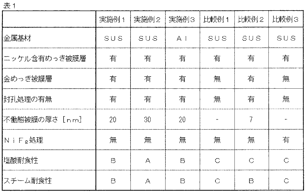
2・・・ニッケル含有めっき被膜層
2a・・・ニッケル-リン合金めっき層(1)
2b・・・ニッケル-リン合金めっき層(2)
3・・・金めっき被膜層
4・・・ピンホール
5・・・不働態被膜
Claims (12)
- 金属基材と、前記金属基材上に形成されたニッケル含有めっき被膜層と、前記ニッケル含有めっき被膜層上に形成された金めっき被膜層とを有し、かつ、
前記金めっき被膜層のピンホールが、厚さ15nm以上の不働態被膜によって封孔されている積層体。 - 前記金属基材が、ステンレス鋼、鉄、アルミニウム、アルミニウム合金、銅および銅合金からなる群より選ばれる少なくとも1つの金属を含む、請求項1に記載の積層体。
- 前記金属基材と前記ニッケル含有めっき被膜層との間に、ニッケルストライク層を有する、請求項1又は請求項2に記載の積層体。
- 前記ニッケル含有めっき被膜層が、リン濃度が8質量%以上10質量%未満のニッケル-リン合金めっき層(1)と、リン濃度が10質量%以上12質量%以下のニッケル-リン合金めっき層(2)とを、前記金属基材側からこの順で含む、請求項1~3のいずれか一項に記載の積層体。
- 前記金めっき被膜層が、置換型金めっき被膜層および還元型金めっき被膜層を、前記ニッケル含有めっき被膜層側からこの順で含む、請求項1~4のいずれか一項に記載の積層体。
- 請求項1~5のいずれか1項に記載の積層体からなる、半導体製造装置の構成部材。
- 金属基材上にニッケル含有めっき被膜層を形成する工程(A)、
前記ニッケル含有めっき被膜層上に金めっき被膜層を形成する工程(B)、および
前記金めっき被膜層のピンホールに、厚さ15nm以上の不働態被膜を形成する封孔処理工程(C)を含む、積層体の製造方法。 - 前記封孔処理工程(C)が、酸素ガス濃度50体積%以上および温度140~200℃の雰囲気下で行われる、請求項7に記載の積層体の製造方法。
- 前記金属基材が、ステンレス鋼、鉄、アルミニウム、アルミニウム合金、銅および銅合金からなる群より選ばれる少なくとも1つの金属を含む、請求項7又は請求項8に記載の積層体の製造方法。
- 前記工程(A)の前に、金属基材に対し電流密度5~20A/dm2の条件でニッケルストライク処理を施す工程を含む、請求項7~9のいずれか一項に記載の積層体の製造方法。
- 前記工程(A)が、リン濃度が8質量%以上10質量%未満のニッケル-リン合金めっき層(1)を形成させる工程(a1)と、該工程(a1)の後に、リン濃度が10質量%以上12質量%以下のニッケル-リン合金めっき層(2)を形成させる工程(a2)とを含む、請求項7~10のいずれか一項に記載の積層体の製造方法。
- 前記工程(B)が、置換型金めっき被膜層を形成させる工程(b1)と、該工程(b1)の後に、還元型金めっき被膜層を形成させる工程(b2)とを含む、請求項7~11のいずれか一項に記載の積層体の製造方法。
Priority Applications (6)
| Application Number | Priority Date | Filing Date | Title |
|---|---|---|---|
| JP2021536881A JP7677146B2 (ja) | 2019-07-31 | 2020-07-09 | 積層体およびその製造方法 |
| CN202080037305.3A CN113874551B (zh) | 2019-07-31 | 2020-07-09 | 层叠体及其制造方法 |
| US17/595,570 US12031213B2 (en) | 2019-07-31 | 2020-07-09 | Laminate |
| KR1020217037195A KR102924902B1 (ko) | 2019-07-31 | 2020-07-09 | 적층체 및 그 제조 방법 |
| SG11202112883PA SG11202112883PA (en) | 2019-07-31 | 2020-07-09 | Laminate and method for producing same |
| EP20848634.0A EP4006201A4 (en) | 2019-07-31 | 2020-07-09 | LAMINATE AND METHOD FOR PRODUCING THEREOF |
Applications Claiming Priority (2)
| Application Number | Priority Date | Filing Date | Title |
|---|---|---|---|
| JP2019-141027 | 2019-07-31 | ||
| JP2019141027 | 2019-07-31 |
Publications (1)
| Publication Number | Publication Date |
|---|---|
| WO2021020064A1 true WO2021020064A1 (ja) | 2021-02-04 |
Family
ID=74230653
Family Applications (1)
| Application Number | Title | Priority Date | Filing Date |
|---|---|---|---|
| PCT/JP2020/026840 Ceased WO2021020064A1 (ja) | 2019-07-31 | 2020-07-09 | 積層体およびその製造方法 |
Country Status (8)
| Country | Link |
|---|---|
| US (1) | US12031213B2 (ja) |
| EP (1) | EP4006201A4 (ja) |
| JP (1) | JP7677146B2 (ja) |
| KR (1) | KR102924902B1 (ja) |
| CN (1) | CN113874551B (ja) |
| SG (1) | SG11202112883PA (ja) |
| TW (1) | TWI737414B (ja) |
| WO (1) | WO2021020064A1 (ja) |
Families Citing this family (2)
| Publication number | Priority date | Publication date | Assignee | Title |
|---|---|---|---|---|
| US20230071985A1 (en) * | 2021-08-24 | 2023-03-09 | Samsung Electronics Co., Ltd. | Substrate processing apparatus and substrate processing method using the same |
| JP2024047995A (ja) * | 2022-09-27 | 2024-04-08 | 富士電機株式会社 | 半導体装置の製造方法 |
Citations (9)
| Publication number | Priority date | Publication date | Assignee | Title |
|---|---|---|---|---|
| JP2954716B2 (ja) | 1990-03-08 | 1999-09-27 | 三菱アルミニウム株式会社 | フッ化不働態膜を形成した工業材料およびその製造方法 |
| JP2000015743A (ja) * | 1998-06-29 | 2000-01-18 | Japan Aviation Electronics Ind Ltd | めっき材 |
| JP3094000B2 (ja) | 1997-09-12 | 2000-10-03 | 昭和電工株式会社 | フッ化表面層を有する金属材料もしくは金属皮膜ならびにフッ化方法 |
| JP2001234360A (ja) * | 2000-02-24 | 2001-08-31 | Ibiden Co Ltd | 高耐食ニッケル−金めっき |
| JP2003293147A (ja) * | 2002-04-04 | 2003-10-15 | Okuno Chem Ind Co Ltd | 金めっき皮膜の後処理方法 |
| JP2004360066A (ja) | 2003-05-09 | 2004-12-24 | Showa Denko Kk | 耐食性材料およびその製造方法 |
| JP2008260646A (ja) | 2007-04-10 | 2008-10-30 | Toshiba Mach Co Ltd | セレン含有ガラス成形用金型及びその製造方法 |
| JP2009057596A (ja) * | 2007-08-31 | 2009-03-19 | Shikoku Chem Corp | 金めっき皮膜の封孔処理剤およびその利用 |
| JP2017021956A (ja) * | 2015-07-09 | 2017-01-26 | 東洋鋼鈑株式会社 | 燃料電池用通電部材、燃料電池セル、燃料電池スタック、及び燃料電池用通電部材の製造方法 |
Family Cites Families (33)
| Publication number | Priority date | Publication date | Assignee | Title |
|---|---|---|---|---|
| JPH05311490A (ja) | 1991-12-25 | 1993-11-22 | Nikko Kinzoku Kk | 金めっき材の封孔処理方法 |
| JPH07258889A (ja) | 1994-03-24 | 1995-10-09 | Nikko Kinzoku Kk | 金めっき材の封孔処理方法 |
| JP2717062B2 (ja) | 1994-03-24 | 1998-02-18 | 日鉱金属株式会社 | 金めっき材の封孔処理方法 |
| US6280597B1 (en) | 1997-09-12 | 2001-08-28 | Showa Denko K.K. | Fluorinated metal having a fluorinated layer and process for its production |
| JP3715818B2 (ja) | 1999-03-24 | 2005-11-16 | 京セラ株式会社 | 光半導体素子収納用パッケージの製造方法 |
| JP2001020077A (ja) | 1999-07-07 | 2001-01-23 | Sony Corp | 無電解めっき方法及び無電解めっき液 |
| US6872470B2 (en) | 2000-02-24 | 2005-03-29 | Ibiden Co., Ltd. | Nickel-gold plating exhibiting high resistance to corrosion |
| JP4932094B2 (ja) | 2001-07-02 | 2012-05-16 | 日本リーロナール有限会社 | 無電解金めっき液および無電解金めっき方法 |
| CN100392151C (zh) | 2003-05-09 | 2008-06-04 | 昭和电工株式会社 | 耐腐蚀性材料及其制造方法 |
| JP4476736B2 (ja) | 2003-08-08 | 2010-06-09 | 昭和電工株式会社 | 黒色膜付基材の製造方法 |
| JP4362599B2 (ja) | 2004-03-05 | 2009-11-11 | Dowaメタルテック株式会社 | 金属部材およびそれを用いた電気接点 |
| EP1767664B1 (en) | 2004-07-09 | 2017-05-17 | JX Nippon Mining & Metals Corporation | Electroless gold plating liquid |
| CN100441738C (zh) | 2004-07-09 | 2008-12-10 | 日矿金属株式会社 | 化学镀金液 |
| JP3948737B2 (ja) | 2005-05-09 | 2007-07-25 | 日本高純度化学株式会社 | 置換型無電解金めっき液 |
| KR100688833B1 (ko) | 2005-10-25 | 2007-03-02 | 삼성전기주식회사 | 인쇄회로기판의 도금층 형성방법 및 이로부터 제조된인쇄회로기판 |
| JP4941650B2 (ja) | 2007-01-11 | 2012-05-30 | 上村工業株式会社 | 無電解金めっき浴のめっき能維持管理方法 |
| EP2554711B1 (en) | 2007-07-31 | 2019-05-15 | JX Nippon Mining & Metals Corporation | Plated article having metal thin film formed by electroless plating |
| JP5209918B2 (ja) | 2007-08-31 | 2013-06-12 | 古河スカイ株式会社 | 平版印刷版用アルミニウム合金板およびその製造方法 |
| JP2010037603A (ja) * | 2008-08-05 | 2010-02-18 | Sumitomo Metal Mining Co Ltd | 接続端子部およびその製造方法 |
| GB2485419B (en) | 2010-11-15 | 2015-02-25 | Semblant Ltd | Method for reducing creep corrosion |
| US8574722B2 (en) * | 2011-05-09 | 2013-11-05 | Tyco Electronics Corporation | Corrosion resistant electrical conductor |
| CN102677114B (zh) | 2012-04-16 | 2015-08-19 | 深圳君泽电子有限公司 | 高耐蚀电镀工艺及用于电子元件的高耐蚀电镀工艺 |
| JP6231982B2 (ja) * | 2012-07-13 | 2017-11-15 | 東洋鋼鈑株式会社 | 無電解金めっき処理方法、および金めっき被覆材料 |
| CN102978671B (zh) | 2012-12-03 | 2016-04-13 | 恒汇电子科技有限公司 | 一种智能卡封装框架的电镀方法 |
| CN103668369A (zh) * | 2014-01-08 | 2014-03-26 | 苏州道蒙恩电子科技有限公司 | 一种提高金属件耐腐蚀性的电镀方法 |
| JP2016160504A (ja) | 2015-03-03 | 2016-09-05 | 学校法人関東学院 | 無電解Ni/Auめっき皮膜の形成方法及びその形成方法で得られた無電解Ni/Auめっき皮膜 |
| JP2017128791A (ja) | 2016-01-19 | 2017-07-27 | Jx金属株式会社 | 無電解Niめっき皮膜を有する構造物、その製造方法および半導体ウェハ |
| JP6326591B2 (ja) | 2016-10-25 | 2018-05-23 | 石原ケミカル株式会社 | 不導態形成性の軽金属上への熱処理式の導電性皮膜形成方法 |
| CN110249074B (zh) * | 2017-02-15 | 2021-11-02 | 三菱电机株式会社 | 半导体元件及其制造方法 |
| CN107059074A (zh) | 2017-05-17 | 2017-08-18 | 江苏金坤科技有限公司 | 一种高效镀金液及镀金处理工艺 |
| CN108359966A (zh) | 2017-09-30 | 2018-08-03 | 深圳市正天伟科技有限公司 | 一种半置换半还原型化学镀金液及其应用方法 |
| CN109628913A (zh) | 2019-01-31 | 2019-04-16 | 湖南互连微电子材料有限公司 | 一种新型化学镍金生产工艺及化学镀镍液 |
| WO2021070561A1 (ja) * | 2019-10-10 | 2021-04-15 | 昭和電工株式会社 | 積層体およびその製造方法 |
-
2020
- 2020-07-09 SG SG11202112883PA patent/SG11202112883PA/en unknown
- 2020-07-09 JP JP2021536881A patent/JP7677146B2/ja active Active
- 2020-07-09 US US17/595,570 patent/US12031213B2/en active Active
- 2020-07-09 CN CN202080037305.3A patent/CN113874551B/zh active Active
- 2020-07-09 EP EP20848634.0A patent/EP4006201A4/en active Pending
- 2020-07-09 WO PCT/JP2020/026840 patent/WO2021020064A1/ja not_active Ceased
- 2020-07-09 KR KR1020217037195A patent/KR102924902B1/ko active Active
- 2020-07-20 TW TW109124385A patent/TWI737414B/zh active
Patent Citations (9)
| Publication number | Priority date | Publication date | Assignee | Title |
|---|---|---|---|---|
| JP2954716B2 (ja) | 1990-03-08 | 1999-09-27 | 三菱アルミニウム株式会社 | フッ化不働態膜を形成した工業材料およびその製造方法 |
| JP3094000B2 (ja) | 1997-09-12 | 2000-10-03 | 昭和電工株式会社 | フッ化表面層を有する金属材料もしくは金属皮膜ならびにフッ化方法 |
| JP2000015743A (ja) * | 1998-06-29 | 2000-01-18 | Japan Aviation Electronics Ind Ltd | めっき材 |
| JP2001234360A (ja) * | 2000-02-24 | 2001-08-31 | Ibiden Co Ltd | 高耐食ニッケル−金めっき |
| JP2003293147A (ja) * | 2002-04-04 | 2003-10-15 | Okuno Chem Ind Co Ltd | 金めっき皮膜の後処理方法 |
| JP2004360066A (ja) | 2003-05-09 | 2004-12-24 | Showa Denko Kk | 耐食性材料およびその製造方法 |
| JP2008260646A (ja) | 2007-04-10 | 2008-10-30 | Toshiba Mach Co Ltd | セレン含有ガラス成形用金型及びその製造方法 |
| JP2009057596A (ja) * | 2007-08-31 | 2009-03-19 | Shikoku Chem Corp | 金めっき皮膜の封孔処理剤およびその利用 |
| JP2017021956A (ja) * | 2015-07-09 | 2017-01-26 | 東洋鋼鈑株式会社 | 燃料電池用通電部材、燃料電池セル、燃料電池スタック、及び燃料電池用通電部材の製造方法 |
Non-Patent Citations (1)
| Title |
|---|
| See also references of EP4006201A4 |
Also Published As
| Publication number | Publication date |
|---|---|
| EP4006201A1 (en) | 2022-06-01 |
| JPWO2021020064A1 (ja) | 2021-02-04 |
| US12031213B2 (en) | 2024-07-09 |
| TWI737414B (zh) | 2021-08-21 |
| JP7677146B2 (ja) | 2025-05-15 |
| TW202113156A (zh) | 2021-04-01 |
| CN113874551B (zh) | 2023-10-03 |
| CN113874551A (zh) | 2021-12-31 |
| KR20210151953A (ko) | 2021-12-14 |
| EP4006201A4 (en) | 2023-11-29 |
| US20220235468A1 (en) | 2022-07-28 |
| KR102924902B1 (ko) | 2026-02-11 |
| SG11202112883PA (en) | 2021-12-30 |
Similar Documents
| Publication | Publication Date | Title |
|---|---|---|
| JP3094000B2 (ja) | フッ化表面層を有する金属材料もしくは金属皮膜ならびにフッ化方法 | |
| JP7677146B2 (ja) | 積層体およびその製造方法 | |
| JP7593324B2 (ja) | 積層体およびその製造方法 | |
| JP2004360066A (ja) | 耐食性材料およびその製造方法 | |
| JP7567797B2 (ja) | 積層体およびその製造方法 | |
| JP3033455B2 (ja) | アルミニウムの無電解ニッケルめっき方法 | |
| JP2008056978A (ja) | 最表面層がフッ化ニッケル膜である金属材料およびその製造方法 | |
| CN100392151C (zh) | 耐腐蚀性材料及其制造方法 | |
| KR102699452B1 (ko) | 알루미늄 또는 알루미늄 합금용 산성 징케이트 조성물 및 이를 이용한 징케이트 처리방법 | |
| JP2006089822A (ja) | 耐ハロゲン腐食性皮膜被覆部材およびその皮膜被覆部材の製造方法 | |
| KR101386019B1 (ko) | 니켈-인-텅스텐-지르코늄 합금 무전해 도금액을 이용한 무전해 도금 방법 | |
| JP2010090823A (ja) | 真空ポンプ用部品およびその製造方法 | |
| JP2018159120A (ja) | ニッケル皮膜の形成方法及び当該方法に使用するためのニッケル溶液 | |
| HK1020442A (en) | Metallic material or film having fluorinated surface layer, and fluorination process |
Legal Events
| Date | Code | Title | Description |
|---|---|---|---|
| 121 | Ep: the epo has been informed by wipo that ep was designated in this application |
Ref document number: 20848634 Country of ref document: EP Kind code of ref document: A1 |
|
| ENP | Entry into the national phase |
Ref document number: 2021536881 Country of ref document: JP Kind code of ref document: A |
|
| ENP | Entry into the national phase |
Ref document number: 20217037195 Country of ref document: KR Kind code of ref document: A |
|
| NENP | Non-entry into the national phase |
Ref country code: DE |
|
| ENP | Entry into the national phase |
Ref document number: 2020848634 Country of ref document: EP Effective date: 20220228 |
|
| WWR | Wipo information: refused in national office |
Ref document number: 1020217037195 Country of ref document: KR |
|
| WWR | Wipo information: refused in national office |
Ref document number: 1020217037195 Country of ref document: KR |
|
| WWC | Wipo information: continuation of processing after refusal or withdrawal |
Ref document number: 1020217037195 Country of ref document: KR |