WO2021106904A1 - Corps lié en graphène - Google Patents
Corps lié en graphène Download PDFInfo
- Publication number
- WO2021106904A1 WO2021106904A1 PCT/JP2020/043747 JP2020043747W WO2021106904A1 WO 2021106904 A1 WO2021106904 A1 WO 2021106904A1 JP 2020043747 W JP2020043747 W JP 2020043747W WO 2021106904 A1 WO2021106904 A1 WO 2021106904A1
- Authority
- WO
- WIPO (PCT)
- Prior art keywords
- graphene
- layer
- plate
- metal
- thickness
- Prior art date
- Legal status (The legal status is an assumption and is not a legal conclusion. Google has not performed a legal analysis and makes no representation as to the accuracy of the status listed.)
- Ceased
Links
Images


Classifications
-
- B—PERFORMING OPERATIONS; TRANSPORTING
- B32—LAYERED PRODUCTS
- B32B—LAYERED PRODUCTS, i.e. PRODUCTS BUILT-UP OF STRATA OF FLAT OR NON-FLAT, e.g. CELLULAR OR HONEYCOMB, FORM
- B32B15/00—Layered products comprising a layer of metal
- B32B15/04—Layered products comprising a layer of metal comprising metal as the main or only constituent of a layer, which is next to another layer of the same or of a different material
-
- B—PERFORMING OPERATIONS; TRANSPORTING
- B32—LAYERED PRODUCTS
- B32B—LAYERED PRODUCTS, i.e. PRODUCTS BUILT-UP OF STRATA OF FLAT OR NON-FLAT, e.g. CELLULAR OR HONEYCOMB, FORM
- B32B9/00—Layered products comprising a layer of a particular substance not covered by groups B32B11/00 - B32B29/00
-
- C—CHEMISTRY; METALLURGY
- C01—INORGANIC CHEMISTRY
- C01B—NON-METALLIC ELEMENTS; COMPOUNDS THEREOF; METALLOIDS OR COMPOUNDS THEREOF NOT COVERED BY SUBCLASS C01C
- C01B32/00—Carbon; Compounds thereof
- C01B32/15—Nano-sized carbon materials
- C01B32/182—Graphene
-
- C—CHEMISTRY; METALLURGY
- C01—INORGANIC CHEMISTRY
- C01B—NON-METALLIC ELEMENTS; COMPOUNDS THEREOF; METALLOIDS OR COMPOUNDS THEREOF NOT COVERED BY SUBCLASS C01C
- C01B32/00—Carbon; Compounds thereof
- C01B32/15—Nano-sized carbon materials
- C01B32/182—Graphene
- C01B32/194—After-treatment
-
- C—CHEMISTRY; METALLURGY
- C04—CEMENTS; CONCRETE; ARTIFICIAL STONE; CERAMICS; REFRACTORIES
- C04B—LIME, MAGNESIA; SLAG; CEMENTS; COMPOSITIONS THEREOF, e.g. MORTARS, CONCRETE OR LIKE BUILDING MATERIALS; ARTIFICIAL STONE; CERAMICS; REFRACTORIES; TREATMENT OF NATURAL STONE
- C04B37/00—Joining burned ceramic articles with other burned ceramic articles or other articles by heating
- C04B37/02—Joining burned ceramic articles with other burned ceramic articles or other articles by heating with metallic articles
-
- H—ELECTRICITY
- H10—SEMICONDUCTOR DEVICES; ELECTRIC SOLID-STATE DEVICES NOT OTHERWISE PROVIDED FOR
- H10W—GENERIC PACKAGES, INTERCONNECTIONS, CONNECTORS OR OTHER CONSTRUCTIONAL DETAILS OF DEVICES COVERED BY CLASS H10
- H10W40/00—Arrangements for thermal protection or thermal control
- H10W40/10—Arrangements for heating
-
- H—ELECTRICITY
- H10—SEMICONDUCTOR DEVICES; ELECTRIC SOLID-STATE DEVICES NOT OTHERWISE PROVIDED FOR
- H10W—GENERIC PACKAGES, INTERCONNECTIONS, CONNECTORS OR OTHER CONSTRUCTIONAL DETAILS OF DEVICES COVERED BY CLASS H10
- H10W40/00—Arrangements for thermal protection or thermal control
- H10W40/20—Arrangements for cooling
- H10W40/25—Arrangements for cooling characterised by their materials
Definitions
- the present invention relates to a graphene junction having a structure in which a graphene-containing carbonaceous member containing a graphene aggregate and a member to be joined are joined.
- the graphene-containing carbonaceous member containing the graphene aggregate is excellent in thermal conductivity, it is particularly suitable as a member constituting the heat radiating member and the heat conductive member.
- it is particularly suitable as a member constituting the heat radiating member and the heat conductive member.
- an insulating layer made of ceramics or the like on the surface of the graphene-containing carbonaceous member containing the graphene aggregate described above, it can be used as an insulating substrate.
- a metal layer By forming a metal layer on the surface of the graphene-containing carbonaceous member, it can be used as a heat conductive plate.
- This heat conductive plate is used in various devices such as a power module and an LED module on which a heating element (power semiconductor element and LED element) is mounted, such as a power generating element (element and a substrate on which the element is mounted). ) And the heat sink.
- Patent Document 1 describes a structure in which graphene sheets are laminated along a first direction, and an intermediate member (metal or ceramics) joined to an end face of the structure in a second direction intersecting the first direction.
- an anisotropic heat conductive element in which the intermediate member (metal or ceramics) is pressure-bonded to the end face via an insert material containing at least titanium.
- a thermal cycle may be applied under the usage environment.
- it may be used in a harsh environment such as an engine room, and a cold cycle under severe conditions with a large temperature difference may be loaded.
- Patent Document 1 described above an intermediate member made of metal or ceramic and a graphene structure are joined via an insert material containing titanium, but depending on the joining conditions, the intermediate member made of metal or ceramic and graphene are joined. It was not possible to firmly join the structure of the above, and there was a risk of peeling when a cold cycle under severe conditions was applied.
- the present invention has been made in view of the above-mentioned circumstances, and the material to be bonded and the graphene-containing carbonaceous member containing a graphene aggregate are firmly bonded to each other, and peeling occurs even when a cold cycle load is applied. It is an object of the present invention to provide a graphene conjugate having excellent thermal cycle reliability.
- the graphene junction has a structure in which a graphene-containing carbonaceous member containing a graphene aggregate and a member to be joined are joined.
- an active metal compound layer is formed on the bonding surface of the graphene-containing carbonaceous member, and the graphene-containing carbonaceous member is contained.
- a Sn-enriched layer having a Sn concentration of 1 mass% or more is formed on the carbonaceous member side, and the thickness of the active metal compound layer is within the range of 0.05 ⁇ m or more and 3 ⁇ m or less. It is said.
- the graphene junction having this configuration, at the junction interface between the graphene-containing carbonaceous member and the member to be joined, one or 2 active metal oxides and active metal carbides are formed on the joint surface of the graphene-containing carbonaceous member. Since the active metal compound layer containing seeds is formed, the bonding surface of the graphene-containing carbonaceous member is sufficiently reacted by the active metal, and the graphene-containing carbon member and the member to be bonded can be firmly bonded. ..
- a Sn-concentrated layer having a Sn concentration of 1 mass% or more is formed on the graphene-containing carbonaceous member side, so that a cooling cycle is performed. It is possible to suppress the peeling of the graphene-containing carbonaceous member and the member to be joined under load, and it is possible to improve the reliability of the thermal cycle. Further, since the bonding material containing Sn is used, the graphene-containing carbonaceous member and the member to be bonded can be firmly bonded under relatively low temperature conditions.
- the thickness of the active metal compound layer is 0.05 ⁇ m or more, the graphene-containing carbonaceous member and the member to be joined can be joined more firmly.
- the thickness of the active metal compound layer is limited to 3 ⁇ m or less, it is possible to suppress the occurrence of cracks in the active metal compound layer during a cold cycle load.
- the thickness of the Sn concentrated layer is within the range of 0.2 ⁇ m or more and 10 ⁇ m or less. In this case, since the thickness of the Sn concentrated layer is 0.2 ⁇ m or more, the reliability of the thermal cycle can be further improved. On the other hand, since the thickness of the Sn-concentrated layer is limited to 10 ⁇ m or less, it is possible to suppress the occurrence of cracks in the Sn-concentrated layer when a cold cycle load is applied.
- the graphene-containing carbonaceous member contains a graphene aggregate formed by depositing single-layer or multi-layer graphene and flat graphite particles, and the flat graphite. It is preferable that the particles are laminated with the graphene aggregate as a binder so that the basal surfaces thereof overlap, and the flat-shaped graphite particles have a structure in which the basal surfaces are oriented in one direction. In this case, it is possible to further improve the heat conduction characteristics of the graphene-containing carbonaceous member.
- the member to be joined may be a ceramic member made of ceramics.
- the member to be joined since the member to be joined is made of ceramics having excellent insulating properties, it can be used as an insulating substrate.
- the member to be joined may be a metal member made of metal.
- the member to be joined since the member to be joined is made of a metal having excellent thermal conductivity, it can be used as a thermal conductive plate.
- the material to be joined and the graphene-containing carbonaceous member containing the graphene aggregate are firmly bonded to each other, and peeling does not occur even under a cold cycle load, so that the cold cycle reliability It is possible to provide an excellent graphene conjugate.
- the graphene conjugate according to the first embodiment of the present invention will be described with reference to FIGS. 1 to 5.
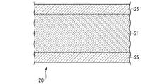
- the graphene joint in the present embodiment is a heat conductive plate 20 having a structure in which a metal plate is joined as a member to be joined to a graphene-containing carbonaceous member containing a graphene aggregate.
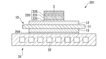
- the power module 1 shown in FIG. 1 includes an insulating circuit board 10, a semiconductor element 3 bonded to one surface side (upper side in FIG. 1) of the insulating circuit board 10 via a solder layer 2, and an insulating circuit board 10.
- a heat conductive plate 20 arranged on the other surface side (lower side in FIG. 1) and a heat sink 31 arranged on the other surface side of the heat conductive plate 20 are provided.
- the insulating circuit board 10 is arranged on the insulating layer 11, the circuit layer 12 arranged on one surface of the insulating layer 11 (upper surface in FIG. 1), and the other surface of the insulating layer 11 (lower surface in FIG. 1). It is provided with the provided metal layer 13.
- the insulating layer 11 prevents electrical connection between the circuit layer 12 and the metal layer 13.
- the insulating layer 11 has highly insulating aluminum nitride (AlN) and aluminum oxide (Al 2 O 3 ). , Silicon nitride (Si 3 N 4 ) and other ceramics.
- the thickness of the insulating layer 11 is set within the range of 0.2 to 1.5 mm, and in the present embodiment, it is set to 0.635 mm.
- the circuit layer 12 is formed by joining a metal plate having excellent conductivity to one surface of the insulating layer 11.
- a metal plate constituting the circuit layer 12 a copper plate made of copper or a copper alloy, specifically, a rolled plate of oxygen-free copper is used.
- a circuit pattern is formed in the circuit layer 12, and one surface (upper surface in FIG. 1) is a mounting surface on which the semiconductor element 3 is mounted.
- the thickness of the metal plate (copper plate) to be the circuit layer 12 is set within the range of 0.1 mm or more and 1.0 mm or less, and in the present embodiment, it is set to 0.6 mm.
- the method of joining the metal plate (copper plate) to be the circuit layer 12 and the insulating layer 11 is not particularly limited, and can be joined using an active metal brazing material or the like.
- the metal layer 13 is formed by joining a metal plate having excellent thermal conductivity to the other surface of the insulating layer 11.
- a copper plate made of copper or a copper alloy specifically, a rolled plate of oxygen-free copper is used.
- the thickness of the metal plate (copper plate) to be the metal layer 13 is set within the range of 0.1 mm or more and 1.0 mm or less, and in the present embodiment, it is set to 0.6 mm.
- the method of joining the metal plate (copper plate) to be the metal layer 13 and the insulating layer 11 is not particularly limited, and can be joined using an active metal brazing material or the like.
- the heat sink 31 is for cooling the above-mentioned insulating circuit board 10, and has a structure in which a plurality of flow paths 32 for flowing a cooling medium (for example, cooling water) are provided.
- the heat sink 31 is preferably made of a material having good thermal conductivity, for example, aluminum or an aluminum alloy, copper or a copper alloy, and in this embodiment, it is made of oxygen-free copper.
- the semiconductor element 3 is made of a semiconductor material such as Si or SiC.
- the semiconductor element 3 is mounted on the circuit layer 12 via, for example, a solder layer 2 made of a Sn—Ag-based, Sn—In-based, or Sn—Ag—Cu-based solder material.
- the graphene junction (heat conductive plate 20) of the present embodiment is interposed between the insulating circuit board 10 and the heat sink 31.
- the outermost layers of both main surfaces of the heat conductive plate 20 are made of oxygen-free copper
- the metal layer 13 of the insulating circuit substrate 10 made of copper and the heat sink 31 made of copper are, for example, Sn-. It is joined via an Ag-based, Sn-In-based, or Sn-Ag-Cu-based solder material.
- the heat conductive plate 20 of the present embodiment has a carbon plate 21 made of a graphene-containing carbonaceous member containing a graphene aggregate and a metal member joined to both main surfaces of the carbon plate 21. Layer 25 and.
- the graphene-containing carbonaceous member constituting the carbon plate 21 contains graphene aggregates formed by depositing single-layer or multi-layer graphene and flat graphite particles so that the flat graphite particles fold their basal surfaces.
- the graphene aggregate has a laminated structure as a binder.
- the flat graphite particles have a basal surface on which a carbon hexagonal network surface appears and an edge surface on which an end portion of the carbon hexagonal network surface appears.
- the flat graphite particles scaly graphite, scaly graphite, earthy graphite, flaky graphite, kiss graphite, pyrolytic graphite, highly oriented pyrolytic graphite and the like can be used.
- the average particle size of the graphite particles as seen from the basal surface is preferably in the range of 10 ⁇ m or more and 1000 ⁇ m or less, and more preferably in the range of 50 ⁇ m or more and 800 ⁇ m or less. By setting the average particle size of the graphite particles within the above range, the thermal conductivity is improved.
- the thickness of the graphite particles is preferably in the range of 1 ⁇ m or more and 50 ⁇ m or less, and more preferably in the range of 1 ⁇ m or more and 20 ⁇ m or less. By setting the thickness of the graphite particles within the above range, the orientation of the graphite particles is appropriately adjusted.
- the thickness of the graphite particles is preferably in the range of 1/1000 to 1/2 of the particle size seen from the basal surface. By setting the thickness of the graphite particles within the above range, excellent thermal conductivity and orientation of the graphite particles can be appropriately adjusted.
- the graphene aggregate is a deposit of single-layer or multi-layer graphene, and the number of layers of the multi-layer graphene is, for example, 100 layers or less, preferably 50 layers or less.
- This graphene aggregate can be produced, for example, by dropping a graphene dispersion in which single-layer or multi-layer graphene is dispersed in a solvent containing lower alcohol or water onto a filter paper and depositing the graphene while separating the solvent. It is possible.
- the average particle size of the graphene aggregate is preferably in the range of 1 ⁇ m or more and 1000 ⁇ m or less. By keeping the average particle size of the graphene aggregate within the above range, the thermal conductivity is improved.
- the thickness of the graphene aggregate is preferably in the range of 0.05 ⁇ m or more and less than 50 ⁇ m. By keeping the thickness of the graphene aggregate within the above range, the strength of the carbonaceous member is ensured.
- the thickness of the carbon plate 21 is preferably in the range of 0.3 mm or more and 3 mm.
- the metal member layer 25 is formed by joining a metal plate to the main surface of the carbon plate 21.
- the metal plate constituting the metal member layer 25 is preferably made of a metal having excellent thermal conductivity, and the metal plate of the present embodiment is made of copper or a copper alloy, more specifically. , It is said to be a rolled plate of oxygen-free copper.
- the thickness of the metal member layer 25 is preferably 50 ⁇ m or more, and more preferably 100 ⁇ m or more.
- the thickness of the metal member layer 25 (thickness of the metal plate) is preferably 5000 ⁇ m or less, and more preferably 3000 ⁇ m or less.
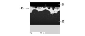
- FIG. 3 shows an observation photograph of the bonding interface between the carbon plate 21 made of graphene-containing carbonaceous member and the metal member layer 25
- FIG. 4 shows the joining of the carbon plate 21 made of graphene-containing carbonaceous member and the metal member layer 25.
- the element mapping diagram of the interface is shown.
- the upper black portion is the carbon plate 21 (graphene-containing carbonaceous member)
- the gray portion located below the carbon plate 21 is the metal member layer 25 (joint member).
- the active metal oxide and the activity are formed on the bonding surface of the carbon plate 21.
- An active metal compound layer 41 containing one or two metal carbides is formed.
- the region where the active metal (Ti) is present is the active metal compound layer 41.
- a Sn-enriched layer 42 having a Sn concentration of 1 mass% or more is formed on the carbon plate 21 side of the bonding interface 40.
- the Sn-enriched region is the Sn-enriched layer 42.
- An alloy layer 43 containing Ag and Cu is formed on the metal member layer 25 side of the bonding interface 40.
- the region where Ag and Cu coexist is the alloy layer 43.
- the active metal compound layer 41 is formed by reacting the active metal contained in the bonding material interposed between the carbon plate 21 and the metal plate with oxygen and carbon at the time of bonding.
- the active metal constituting the active metal compound layer 41 for example, one kind or two or more kinds selected from Ti, Zr, Hf, and Nb can be used.
- the active metal is Ti
- the active metal compound layer 41 contains one or two types of titanium oxide (Ti—O) and titanium carbide (Ti—C). ..
- the thickness t1 of the active metal compound layer 41 is 0.05 ⁇ m or more, the reaction between the bonding material and the carbon plate 21 is promoted, and the bonding strength of the carbon plate 21 is sufficiently secured.
- the thickness t1 of the active metal compound layer 41 is 3 ⁇ m or less, the occurrence of cracks in the active metal compound layer 41 can be suppressed when the active metal compound layer 41 is loaded. Therefore, in the present embodiment, the thickness t1 of the active metal compound layer 41 is set to be within the range of 0.05 ⁇ m or more and 3 ⁇ m or less.
- the thickness t1 of the active metal compound layer 41 is more preferably 0.1 ⁇ m or more, and even more preferably 0.2 ⁇ m or more.
- the thickness t1 of the active metal compound layer 41 is more preferably 2 ⁇ m or less, and more preferably 1.8 ⁇ m or less.
- the Sn concentrated layer 42 is formed by segregating Sn contained in the bonding material interposed between the carbon plate 21 and the metal plate toward the carbon plate 21 at the time of bonding.
- Sn concentrated layer 42 a cross-sectional observation sample near the interface of the graphene / ceramics joint was taken, and EPMA (for example, JXA-8530F manufactured by JEOL Ltd., acceleration voltage: 15 kV, spot diameter: 1 ⁇ m or less) was used. It can be specified by acquiring the EPMA mapping.
- the thickness t2 of the Sn concentrated layer 42 is 0.2 ⁇ m or more, the reliability of the thermal cycle can be reliably improved.
- the thickness t2 of the Sn-concentrated layer 42 is limited to 10 ⁇ m or less, it is possible to suppress the occurrence of cracks in the Sn-concentrated layer 42 when a cold cycle load is applied. Therefore, in the present embodiment, the thickness t2 of the Sn concentrated layer 42 is preferably in the range of 0.2 ⁇ m or more and 10 ⁇ m or less.
- the thickness t2 of the Sn concentrated layer 42 is more preferably 0.5 ⁇ m or more, and more preferably 0.7 ⁇ m or more.
- the thickness t2 of the Sn concentrated layer 42 is more preferably 5 ⁇ m or less, and more preferably 3 ⁇ m or less.
- the alloy layer 43 is formed by the reaction of Ag and Cu contained in the bonding material interposed between the carbon plate 21 and the metal plate at the time of bonding.
- the metal member layer 25 metal plate
- the alloy layer 43 is formed by diffusing Ag of the bonding material on the metal member layer 25 (metal plate) side. .. Therefore, in the alloy layer 43 and the metal member layer 25, there is a concentration gradient of Ag. When Ag is sufficiently diffused to the metal member layer 25 side and solid-solved in the metal member layer 25, the alloy layer 43 may not be formed.
- the thickness t3 of the alloy layer 43 is 1 ⁇ m or more, the reaction of the bonding material is sufficiently promoted, and the bonding strength between the carbon plate 21 and the metal member layer 25 is sufficiently secured.
- the thickness t3 of the alloy layer 43 is 20 ⁇ m or less, it is possible to suppress the occurrence of cracks in the alloy layer 43 during a cold cycle load. Therefore, in the present embodiment, the thickness t3 of the alloy layer 43 is preferably in the range of 1 ⁇ m or more and 20 ⁇ m or less.
- the thickness t3 of the alloy layer 43 is more preferably 2 ⁇ m or more, and more preferably 3 ⁇ m or more.
- the thickness t3 of the alloy layer 43 is more preferably 10 ⁇ m or less, and more preferably 8 ⁇ m or less.
- Carbon plate forming step S01 First, the above-mentioned flat graphite particles and graphene aggregates are weighed so as to have a predetermined blending ratio, and these are mixed by an existing mixing device such as a ball mill. A molded product is obtained by filling the obtained mixture in a mold having a predetermined shape and pressurizing the mixture. Heating may be performed during pressurization. Then, the obtained molded product is cut out to obtain a carbon plate 21.
- the pressure at the time of molding is preferably in the range of 20 MPa or more and 1000 MPa or less, and more preferably in the range of 100 MPa or more and 300 MPa or less.
- the temperature at the time of molding is preferably in the range of 50 ° C. or higher and 300 ° C. or lower.
- the pressurization time is preferably in the range of 0.5 minutes or more and 10 minutes or less.
- a metal plate to be a metal member layer 25 is laminated on both main surfaces of the carbon plate 21 via a bonding material.
- a bonding material a material containing Ag, Cu, Sn, and an active metal (Ti in this embodiment) is used.
- the bonding material may be in the form of a paste or in the form of a foil. Further, for example, a Cu—Ag—Sn alloy and an active metal may be laminated.
- the bonding material contains Cu in the range of 18 mass% or more and 34 mass% or less, Sn in the range of 3 mass% or more and 10 mass% or less, Ti in the range of 0.3 mass% or more and 7 mass% or less, and the balance is Ag and The composition used as an unavoidable impurity is used.
- Metal plate joining step S03 Next, the metal plate and the carbon plate 21 laminated via the bonding material are pressed in the stacking direction, heated, and then cooled to join the metal plate and the carbon plate 21 to form the metal member layer 25.
- the heating temperature is preferably in the range of 740 ° C. or higher and 900 ° C. or lower.
- the holding time at the heating temperature is preferably in the range of 20 minutes or more and 180 minutes or less.
- the pressurizing pressure is preferably in the range of 0.1 MPa or more and 3.5 MPa or less.
- the atmosphere is preferably a non-oxidizing atmosphere such as a reduced pressure atmosphere or a nitrogen gas atmosphere.
- the active metal (Ti in the present embodiment) contained in the joining material reacts with oxygen and carbon, so that the active metal compound layer 41 is formed on the joining surface of the carbon plate 21.
- the Sn-concentrated layer 42 is formed by segregating Sn contained in the bonding material toward the carbon plate 21 side.
- the alloy layer 43 is formed on the metal member layer 25 side by reacting Cu and Ag contained in the bonding material and diffusing Ag on the metal plate (metal member layer 25) side.
- the graphene joint (heat conductive plate 20) of the present embodiment is manufactured.
- the active metal oxide is formed on the joint surface of the carbon plate 21 at the joint interface between the carbon plate 21 and the metal member layer 25. Since the active metal compound layer 41 containing one or two of (Ti-O) and the active metal carbide (Ti-C) is formed, the graphene-containing carbonaceous member is made of the active metal (Ti in this embodiment). The joint surface of the carbon plate 21 made of the carbon plate 21 is sufficiently reacted, and the carbon plate 21 and the metal member layer 25 (metal plate) are firmly joined.
- Sn contained in the bonding material is segregated on the carbon plate 21 side to form a Sn-enriched layer 42 having a Sn concentration of 1 mass% or more. Therefore, it is possible to prevent the carbon plate 21 and the metal member layer 25 from peeling off when a cold cycle load is applied, and it is possible to improve the reliability of the cold cycle. Since a bonding material containing Sn is used, the carbon plate 21 and the metal member layer 25 (metal plate) can be firmly bonded under relatively low temperature conditions.
- the thickness of the active metal compound layer 41 is 0.05 ⁇ m or more, it is possible to firmly join the carbon plate 21 made of a graphene-containing carbonaceous member and the metal member layer 25. Become.
- the thickness of the active metal compound layer 41 is limited to 3 ⁇ m or less, it is possible to suppress the occurrence of cracks in the active metal compound layer 41 when loaded with a cold cycle.
- the thickness of the Sn concentrated layer 42 when the thickness of the Sn concentrated layer 42 is 0.2 ⁇ m or more, the reliability of the thermal cycle can be reliably improved.
- the thickness of the Sn-concentrated layer 42 when the thickness of the Sn-concentrated layer 42 is limited to 10 ⁇ m or less, it is possible to suppress the occurrence of cracks in the Sn-concentrated layer 42 when a cold cycle load is applied.
- the graphene-containing carbonaceous member constituting the carbon plate 21 contains a graphene aggregate formed by depositing single-layer or multi-layer graphene and flat graphite particles, and the flat graphite particles are formed.
- the carbon plate 21 graphene-containing carbon
- the heat conductive plate 20 is arranged between the insulating circuit board 10 and the heat sink 31, the insulating circuit is formed in the metal member layer 25 formed on one main surface side of the heat conductive plate 20.
- the heat from the substrate 10 can be spread in the plane direction, the heat can be efficiently transferred in the thickness direction, and the heat can be dissipated in the heat sink 31. Therefore, the power module 1 having excellent heat dissipation characteristics can be configured.
- the graphene junction in the present embodiment is an insulating substrate 120 having a structure in which a ceramic plate is bonded as a member to be bonded to a graphene-containing carbonaceous member containing a graphene aggregate.
- the ceramic plate 125 and the carbon plate 121 made of a graphene-containing carbonaceous member containing a graphene aggregate are bonded to both sides of the ceramic plate 125, respectively. It is said to have a structure.
- the graphene-containing carbonaceous member constituting the carbon plate 121 contains graphene aggregates formed by depositing single-layer or multi-layer graphene and flat graphite particles, and is flat graphite. It is preferable that the particles have a structure in which graphene aggregates are laminated as a binder so that their basal surfaces overlap.
- the thickness of the carbon plate 121 is preferably in the range of 0.3 mm or more and 3 mm.
- the ceramic plate 125 is made of ceramics having excellent insulating properties, for example, aluminum nitride (AlN), aluminum oxide (Al 2 O 3 ), silicon nitride (Si 3 N 4 ), and the like.
- the thickness of the ceramic plate 125 is preferably 100 ⁇ m or more, and more preferably 250 ⁇ m or more.
- the ceramic plate 125 is preferably 1500 ⁇ m or less, and more preferably 1000 ⁇ m or less.
- FIG. 7 shows an observation photograph of the bonding interface between the carbon plate 121 made of a graphene-containing carbonaceous member and the ceramic plate 125.
- the upper black portion is the carbon plate 121 (graphene-containing carbonaceous member)
- the gray portion located below the carbon plate 121 is the ceramic plate 125 (joint member).
- one kind of active metal oxide and active metal carbide is formed on the bonding surface of the carbon plate 121 as in the first embodiment.
- an active metal compound layer containing two types is formed.
- a Sn-enriched layer having a Sn concentration of 1 mass% or more is formed on the carbon plate 121 side of the bonding interface 140.
- An alloy layer containing Ag and Cu is formed on the ceramic plate 125 side of the bonding interface 140.
- the active metal compound layer is formed by reacting the active metal (Ti in this embodiment) contained in the bonding material interposed between the carbon plate 121 and the ceramic plate 125 at the time of bonding with oxygen and carbon.
- the active metal compound layer in the present embodiment has the same structure as that in the first embodiment.
- the thickness t11 of the active metal compound layer is in the range of 0.05 ⁇ m or more and 3 ⁇ m or less.
- the Sn-enriched layer is formed by segregating Sn contained in the bonding material interposed between the carbon plate 121 and the ceramic plate 125 toward the carbon plate 121 at the time of bonding.
- the Sn-enriched layer in this embodiment has the same structure as that in the first embodiment.
- the thickness t12 of the Sn concentrated layer is preferably in the range of 0.2 ⁇ m or more and 10 ⁇ m or less.
- the alloy layer is formed by the reaction of Ag and Cu contained in the bonding material interposed between the carbon plate 121 and the ceramic plate 125 at the time of bonding.
- Ag of the bonding material does not diffuse to the ceramic plate 125 side, and the alloy layer tends to be formed thicker than that of the first embodiment.
- the thickness t13 of the alloy layer is preferably in the range of 1 ⁇ m or more and 20 ⁇ m or less.
- the thickness t13 of the alloy layer is more preferably 2 ⁇ m or more, and more preferably 3 ⁇ m or more.
- the thickness t13 of the alloy layer is more preferably 10 ⁇ m or less, and more preferably 8 ⁇ m or less.
- the flat graphite particles and the graphene aggregate are weighed so as to have a predetermined blending ratio, and this is mixed by an existing mixing device such as a ball mill, and the obtained mixture is obtained. Is filled in a mold having a predetermined shape and pressed to form a molded product, and the obtained molded product is cut out.
- the graphene aggregate formed by depositing single-layer or multi-layer graphene and the flat graphite particles are included, and the flat graphite particles are laminated with the graphene aggregate as a binder so that the basal surfaces thereof are folded. Therefore, it is possible to obtain a graphene-containing carbonaceous member (carbon plate 121) having a structure in which the basal surface of the flat-shaped graphite particles is oriented in one direction.
- the carbon plate 121 is laminated on both main surfaces of the ceramic plate 125 via a bonding material.
- a bonding material a material containing Ag, Cu, Sn, and an active metal (Ti in this embodiment) is used as in the first embodiment.
- the heating temperature is preferably in the range of 750 ° C. or higher and 900 ° C. or lower.
- the holding time at the heating temperature is preferably in the range of 20 minutes or more and 180 minutes or less.
- the pressurizing pressure is preferably in the range of 0.1 MPa or more and 3.5 MPa or less.
- the atmosphere is preferably a non-oxidizing atmosphere such as a reduced pressure atmosphere or a nitrogen gas atmosphere.
- the active metal (Ti in the present embodiment) contained in the joining material reacts with oxygen and carbon to form an active metal compound layer on the joining surface of the carbon plate 121.
- the Sn contained in the bonding material segregates toward the carbon plate 121 side to form a Sn concentrated layer.
- An alloy layer is formed on the ceramic plate 125 side by the reaction between Cu and Ag contained in the bonding material.
- the graphene junction (insulated substrate 120) according to the present embodiment is manufactured.
- an active metal compound layer is formed on the joint surface of the carbon plate 121 at the joint interface between the carbon plate 121 and the ceramic plate 125. Therefore, the bonding surface of the carbon plate 121 made of the graphene-containing carbonaceous member is sufficiently reacted by the active metal (Ti in the present embodiment), and the carbon plate 121 and the ceramic plate 125 are firmly bonded. ..
- the thickness t11 of the active metal compound layer is 0.05 ⁇ m or more, it is possible to firmly join the carbon plate 121 made of the graphene-containing carbonaceous member and the ceramic plate 125. ..
- the thickness t11 of the active metal compound layer is limited to 3 ⁇ m or less, it is possible to suppress the occurrence of cracks in the active metal compound layer when loaded with a cold cycle.
- the thickness t12 of the Sn concentrated layer when the thickness t12 of the Sn concentrated layer is 0.2 ⁇ m or more, the reliability of the thermal cycle can be reliably improved.
- the thickness t12 of the Sn-concentrated layer is limited to 10 ⁇ m or less, it is possible to suppress the occurrence of cracks in the Sn-concentrated layer when a cold cycle load is applied.
- the graphene-containing carbonaceous member constituting the carbon plate 121 contains a graphene aggregate formed by depositing single-layer or multi-layer graphene and flat graphite particles, and the flat graphite particles are formed.
- the carbon plate 121 graphene-containing carbon
- the insulating substrate 120 of the present embodiment includes the ceramic plate 125, it has excellent insulating properties. Since it is provided with a carbon plate 121 made of a graphene-containing carbonaceous member, it has excellent thermal conductivity. Therefore, for example, it can be used as the insulating layer 11 of the power module 1 (insulated circuit board 10) shown in FIG.
- a semiconductor element (power semiconductor element) is mounted on the circuit layer of the insulated circuit board to form a power module, but the present embodiment is not limited to this.
- an LED element may be mounted on an insulated circuit board to form an LED module
- a thermoelectric element may be mounted on a circuit layer of an insulated circuit board to form a thermoelectric module.
- the power module 1 having a structure in which the heat conductive plate 20 is arranged between the insulating circuit board 10 and the heat sink 31 has been described as an example, but the present invention is limited to this. There is no particular limitation on the method of using the graphene conjugate of the present invention.
- the power module 201 has a structure in which the heat conductive plate 220 is arranged between the circuit layer 12 of the insulating circuit board 10 and the semiconductor element 3. Good.
- the power module 301 using the heat conductive plate 320 may be used as the metal layer of the insulating circuit board 310.
- the power module 401 using the heat conductive plate 420 may be used as the circuit layer and the metal layer of the insulating circuit board 410.
- the power module 201 shown in FIG. 9 is different from the power module 1 shown in FIG. 1 in that a heat conductive plate 220 is used instead of the solder layer 2 and a solder layer 204 is used instead of the heat conductive plate 20.
- a heat conductive plate 220 is used instead of the solder layer 2 and a solder layer 204 is used instead of the heat conductive plate 20.
- Other configurations are the same as those of the power module 1 shown in FIG. 1, and the same reference numerals are given to the same configurations, and the description thereof will be omitted.
- the heat conductive plate 220 includes a carbon plate 221 made of a graphene-containing carbonaceous member containing a graphene aggregate, and a metal member layer 225 joined to both main surfaces of the carbon plate 221.
- the heat conductive plate 220, the carbon plate 221 and the metal member layer 225 have the same configurations as the heat conductive plate 20, the carbon plate 21 and the metal member layer 25 of the first embodiment, respectively.
- the metal layer 13 and the heat sink 31 are joined via a solder layer 204 made of, for example, a Sn—Ag-based, Sn—In-based, or Sn—Ag—Cu-based solder material.
- the heat conductive plate 220 is arranged between the circuit layer 12 of the insulating circuit board 10 and the semiconductor element 3, the heat from the semiconductor element 3 can be spread in the plane direction, and this heat can be spread. Is efficiently transmitted in the thickness direction, and heat can be dissipated in the heat sink 31. Therefore, the power module 201 having excellent heat dissipation characteristics can be configured.
- the power module 301 shown in FIG. 10 is an insulating circuit board 310 in which a carbon plate 321 is used as a metal layer instead of the metal layer 13, and the insulating circuit board 310 and the heat sink 31 are joined by using an active metal brazing material or the like.
- the point is different from the power module 1 shown in FIG.
- Other configurations are the same as those of the power module 1 shown in FIG. 1, and the same reference numerals are given to the same configurations, and the description thereof will be omitted.
- the carbon plate 321 has the same configuration as the carbon plate 21 of the first embodiment or the carbon plate 121 of the second embodiment.
- the insulating layer 11 and the carbon plate 321 are joined in the same configuration as the second graphene joint (insulating substrate 120).
- the carbon plate 321 and the heat sink 31 are joined in the same configuration as the first graphene joint (heat conductive plate 20).
- a carbon plate 321 is used as the metal layer of the insulating circuit board 310, and the insulating layer 11 and the carbon plate 321 are joined in the same configuration as the second graphene junction (insulating substrate 120), and carbon is used. Since the plate 321 and the heat sink 31 are joined in the same configuration as the first graphene joint (heat conductive plate 20), the heat from the insulating circuit board 10 can be spread in the plane direction, and this heat can be dissipated. It can be efficiently transmitted in the thickness direction and dissipated in the heat sink 31. Therefore, the power module 301 having excellent heat dissipation characteristics can be configured.
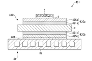
- the power module 401 shown in FIG. 11 is an insulating circuit board 410 in which a heat conductive plate 420a is used as a circuit layer instead of the circuit layer 12, and a heat conductive plate 420b is used as a metal layer instead of the metal layer 13. It differs from the power module 1 shown in FIG. 1 in that the solder layer 404 is used instead of the plate 20.
- Other configurations are the same as those of the power module 1 shown in FIG. 1, and the same reference numerals are given to the same configurations, and the description thereof will be omitted.
- the heat conductive plate 420a includes a carbon plate 421a made of a graphene-containing carbonaceous member containing a graphene aggregate, and a metal member layer 425a joined to one surface side (upper side of FIG. 11) of the carbon plate 421a. I have.
- the heat conductive plate 420a, the carbon plate 421a, and the metal member layer 425a have the same configurations as the heat conductive plate 20, the carbon plate 21, and the metal member layer 25 of the first embodiment, respectively.
- the heat conductive plate 420b includes a carbon plate 421b made of a graphene-containing carbonaceous member containing a graphene aggregate, and a metal member layer 425b joined to the other surface side (lower side of FIG.
- the heat conductive plate 420b, the carbon plate 421b, and the metal member layer 425b have the same configurations as the heat conductive plate 20, the carbon plate 21, and the metal member layer 25 of the first embodiment, respectively.
- the carbon plate 421a and the insulating layer 11, and the insulating layer 11 and the carbon plate 421b are each joined in the same configuration as the second graphene joint (insulating substrate 120).
- the heat conductive plate 420b and the heat sink 31 are joined via a solder layer 404 made of, for example, a Sn—Ag-based, Sn—In-based, or Sn—Ag—Cu-based solder material.
- the heat conductive plate 420a is used as a circuit layer
- the heat conductive plate 420b is used as a metal layer
- the carbon plate 421a and the insulating layer 11 and the insulating layer 11 and the carbon plate 421b are each a second graphene joint. Since they are joined in the same configuration as (insulated substrate 120), heat from the semiconductor element 3 and the insulating circuit board 410 can be spread in the plane direction, and this heat is efficiently transferred in the thickness direction to heat sink 31. Can dissipate heat in. Therefore, the power module 401 having excellent heat dissipation characteristics can be configured.
- the flat graphite particles and the graphene aggregate are mixed at a predetermined compounding ratio, mixed, and heated by pressure to form the flat graphite particles on the basal surface thereof.
- a molded body having a structure in which graphene aggregates were laminated as a binder was obtained so as to be folded over.
- the obtained molded product was cut out to obtain a carbon plate (40 mm ⁇ 40 mm ⁇ thickness 1.5 mm).
- a copper plate (40 mm ⁇ 40 mm) made of rolled oxygen-free copper is interposed on one surface of this carbon plate via a bonding material (thickness variation) having a composition of Ag-28 mass% Cu-5 mass% Sn-3 mass% Ti. ⁇ Thickness 0.3 mm) or ceramic plate (40 mm ⁇ 40 mm ⁇ thickness 0.3 mm) was laminated, and the carbon plate and the copper plate were joined under the conditions shown in Table 1. Then, the bonding interface between the carbon plate and the copper plate was observed, and the thickness of the active metal compound layer and the thickness of the Sn concentrated layer were confirmed.
- the thickness of the active metal compound layer is determined by collecting an observation sample from the central part of the graphene / copper junction and scanning the junction interface with a scanning transmission electron microscope (FEI Titan ChemiSTEM (with EDS detector)). Observation was performed under the conditions of a magnification of 40,000 times and an acceleration voltage of 200 kV, and mapping was performed using an energy dispersive X-ray analysis method (NSS7 manufactured by Thermo Scientific Co., Ltd.) to determine the area of the region where the active metal exists. The measurement was performed, the value divided by the width of the measurement field was obtained, and the average value of the five fields was taken as the thickness of the active metal compound layer. As measurement points, a total of 5 points were observed, which are the region of the center point of the insulated circuit board and the region of four vertices of a 20 mm ⁇ 20 mm quadrangle centered on that point.
- a cross-sectional observation sample near the bonding interface of the graphene / copper junction was collected, and EPMA (JXA-8530F manufactured by JEOL Ltd., acceleration voltage: 15 kV, spot diameter: 1 ⁇ m or less) was applied.
- EPMA mapping was obtained using EPMA mapping, the area where Sn was 1 mass% or more was regarded as a Sn-enriched layer, the area was measured, the value divided by the width of the measurement field was obtained, and the average value of the five fields was Sn-concentrated.
- the thickness of the chemical layer was used. As measurement points, a total of 5 points were observed, which are the region of the center point of the insulated circuit board and the region of four vertices of a 20 mm ⁇ 20 mm quadrangle centered on that point.
- the obtained conjugate was loaded with 2000 cycles of a cold heat cycle of ⁇ 55 ° C. ⁇ 30 minutes ⁇ ⁇ 175 ° C. ⁇ 30 minutes. Then, the bonding ratio at the interface between the carbon plate and the copper plate was evaluated using an ultrasonic flaw detector (FineSAT200 manufactured by Hitachi Power Solutions, Ltd.) and calculated from the following formula.
- the initial joining area was defined as the area to be joined before joining. In the image obtained by binarizing the ultrasonic flaw detection image, the peeling is shown by the white part in the joint portion, and therefore the area of this white part is defined as the peeling area (non-joint part area).
- (Joining ratio) ⁇ (Initial joining area)-(Non-joining area) ⁇ / (Initial joining area) x 100
- Example 1-6 of the present invention in which the Sn-concentrated layer was formed and the thickness of the active metal compound layer was in the range of 0.05 ⁇ m or more and 3 ⁇ m or less, the bonding ratio after the thermal cycle test was high. It was 80% or more, and the thermal cycle reliability was excellent.
- the material to be bonded and the graphene-containing carbonaceous member containing the graphene aggregate are firmly bonded, and peeling does not occur even under a cold cycle load. It was confirmed that it is possible to provide a graphene conjugate having excellent thermal cycle reliability.
- the material to be bonded and the graphene-containing carbonaceous member containing the graphene aggregate are firmly bonded to each other, peeling does not occur even under a cold cycle load, and the cold cycle reliability is excellent.
- Graphene conjugates can be provided.
Landscapes
- Chemical & Material Sciences (AREA)
- Engineering & Computer Science (AREA)
- Organic Chemistry (AREA)
- Materials Engineering (AREA)
- Ceramic Engineering (AREA)
- Nanotechnology (AREA)
- Inorganic Chemistry (AREA)
- Structural Engineering (AREA)
- Cooling Or The Like Of Semiconductors Or Solid State Devices (AREA)
Abstract
L'invention concerne un corps lié en graphène (20) qui a une structure dans laquelle un élément carboné contenant du graphène (21) contenant un ensemble graphène et un élément (25) à lier sont liés l'un à l'autre ; et au niveau d'une interface de liaison (40) entre l'élément carboné contenant du graphène (21) et l'élément (25) à lier, une couche de composé métallique actif (41) contenant un oxyde métallique actif et un ou deux carbures métalliques actifs est formée au niveau de la surface de liaison de l'élément carboné contenant du graphène (21), tandis qu'une couche enrichie en Sn (42) ayant une concentration en Sn de 1 % en masse ou plus est formée sur le côté de l'élément carboné contenant du graphène (21).
Applications Claiming Priority (4)
| Application Number | Priority Date | Filing Date | Title |
|---|---|---|---|
| JP2019-212090 | 2019-11-25 | ||
| JP2019212090 | 2019-11-25 | ||
| JP2020-190318 | 2020-11-16 | ||
| JP2020190318A JP7563124B2 (ja) | 2019-11-25 | 2020-11-16 | グラフェン接合体 |
Publications (1)
| Publication Number | Publication Date |
|---|---|
| WO2021106904A1 true WO2021106904A1 (fr) | 2021-06-03 |
Family
ID=76130529
Family Applications (1)
| Application Number | Title | Priority Date | Filing Date |
|---|---|---|---|
| PCT/JP2020/043747 Ceased WO2021106904A1 (fr) | 2019-11-25 | 2020-11-25 | Corps lié en graphène |
Country Status (1)
| Country | Link |
|---|---|
| WO (1) | WO2021106904A1 (fr) |
Cited By (1)
| Publication number | Priority date | Publication date | Assignee | Title |
|---|---|---|---|---|
| US20220238414A1 (en) * | 2021-01-27 | 2022-07-28 | CTRON Advanced Material Co., Ltd | Thermal conductive structure and electronic device |
Citations (4)
| Publication number | Priority date | Publication date | Assignee | Title |
|---|---|---|---|---|
| JP2010046700A (ja) * | 2008-08-22 | 2010-03-04 | Toyota Central R&D Labs Inc | 接合体およびその製造方法 |
| WO2010087432A1 (fr) * | 2009-01-29 | 2010-08-05 | 株式会社オクテック | Corps de base dissipateur thermique et dispositif électronique l'utilisant |
| JP2015532531A (ja) * | 2012-09-25 | 2015-11-09 | モーメンティブ・パフォーマンス・マテリアルズ・インク | バルクグラフェン材料を含む熱管理アセンブリ |
| JP2018518020A (ja) * | 2015-05-15 | 2018-07-05 | モーメンティブ・パフォーマンス・マテリアルズ・インク | 熱管理のための熱分解グラファイトを用いた発光ダイオードアセンブリ |
-
2020
- 2020-11-25 WO PCT/JP2020/043747 patent/WO2021106904A1/fr not_active Ceased
Patent Citations (4)
| Publication number | Priority date | Publication date | Assignee | Title |
|---|---|---|---|---|
| JP2010046700A (ja) * | 2008-08-22 | 2010-03-04 | Toyota Central R&D Labs Inc | 接合体およびその製造方法 |
| WO2010087432A1 (fr) * | 2009-01-29 | 2010-08-05 | 株式会社オクテック | Corps de base dissipateur thermique et dispositif électronique l'utilisant |
| JP2015532531A (ja) * | 2012-09-25 | 2015-11-09 | モーメンティブ・パフォーマンス・マテリアルズ・インク | バルクグラフェン材料を含む熱管理アセンブリ |
| JP2018518020A (ja) * | 2015-05-15 | 2018-07-05 | モーメンティブ・パフォーマンス・マテリアルズ・インク | 熱管理のための熱分解グラファイトを用いた発光ダイオードアセンブリ |
Cited By (1)
| Publication number | Priority date | Publication date | Assignee | Title |
|---|---|---|---|---|
| US20220238414A1 (en) * | 2021-01-27 | 2022-07-28 | CTRON Advanced Material Co., Ltd | Thermal conductive structure and electronic device |
Similar Documents
| Publication | Publication Date | Title |
|---|---|---|
| JP6904088B2 (ja) | 銅/セラミックス接合体、及び、絶縁回路基板 | |
| CN109315061B (zh) | 陶瓷电路基板及陶瓷电路基板的制造方法 | |
| JP6965768B2 (ja) | 銅/セラミックス接合体、絶縁回路基板、及び、銅/セラミックス接合体の製造方法、絶縁回路基板の製造方法 | |
| US8116084B2 (en) | Method for manufacturing power module substrate, power module substrate, and power module | |
| CN104067386A (zh) | 功率模块用基板、自带散热器的功率模块用基板、功率模块、功率模块用基板的制造方法以及铜部件接合用浆料 | |
| CN104718616A (zh) | 自带散热器的功率模块用基板、自带散热器的功率模块及自带散热器的功率模块用基板的制造方法 | |
| JP7563124B2 (ja) | グラフェン接合体 | |
| KR20150092150A (ko) | 파워 모듈용 기판, 히트 싱크가 부착된 파워 모듈용 기판, 파워 모듈, 파워 모듈용 기판의 제조 방법, 동판 접합용 페이스트, 및 접합체의 제조 방법 | |
| JP6908173B2 (ja) | 銅/セラミックス接合体、絶縁回路基板、及び、銅/セラミックス接合体の製造方法、絶縁回路基板の製造方法 | |
| JPWO2020091008A1 (ja) | 金属層付き炭素質部材、及び、熱伝導板 | |
| WO2021100860A1 (fr) | Ensemble céramique/cuivre/graphène et procédé pour sa fabrication et structure de liaison céramique/cuivre/graphène | |
| WO2021112060A1 (fr) | Corps lié de cuivre/céramique, carte de circuit isolé, procédé de production d'un corps lié de cuivre/céramique, et procédé de production d'une carte de circuit isolé | |
| WO2021149802A1 (fr) | Corps assemblé cuivre/graphène et son procédé de fabrication, et structure assemblée cuivre/graphène | |
| CN108780784B (zh) | 带Ag基底层的金属部件、带Ag基底层的绝缘电路基板、半导体装置、带散热器的绝缘电路基板及带Ag基底层的金属部件的制造方法 | |
| JP7533124B2 (ja) | グラフェン含有炭素質部材/セラミックス接合体、および、銅/グラフェン含有炭素質部材/セラミックス接合体 | |
| JP6947318B2 (ja) | 銅/グラフェン接合体とその製造方法、および銅/グラフェン接合構造 | |
| JP2019081690A (ja) | 接合体、及び、絶縁回路基板 | |
| JP7552282B2 (ja) | セラミックス/銅/グラフェン接合体とその製造方法、およびセラミックス/銅/グラフェン接合構造 | |
| WO2021106904A1 (fr) | Corps lié en graphène | |
| WO2023008562A1 (fr) | Corps collé cuivre/céramique et circuit imprimé isolé | |
| WO2021090759A1 (fr) | Ensemble élément carboné/céramique contenant du graphène et ensemble élément carboné/céramique contenant du cuivre/graphène | |
| WO2019082970A1 (fr) | Corps lié et carte de circuit imprimé isolée | |
| WO2023286858A1 (fr) | Ensemble cuivre/céramique, substrat de circuit isolant, procédé de production pour ensemble cuivre/céramique, et procédé de production pour substrat de circuit isolant | |
| CN117897366B (zh) | 铜-陶瓷接合体及绝缘电路基板 | |
| TWI801689B (zh) | 接合體、附散熱片絕緣電路基板、及散熱片 |
Legal Events
| Date | Code | Title | Description |
|---|---|---|---|
| 121 | Ep: the epo has been informed by wipo that ep was designated in this application |
Ref document number: 20893270 Country of ref document: EP Kind code of ref document: A1 |
|
| NENP | Non-entry into the national phase |
Ref country code: DE |
|
| 122 | Ep: pct application non-entry in european phase |
Ref document number: 20893270 Country of ref document: EP Kind code of ref document: A1 |