WO2021106928A1 - 窒化物半導体素子 - Google Patents
窒化物半導体素子 Download PDFInfo
- Publication number
- WO2021106928A1 WO2021106928A1 PCT/JP2020/043810 JP2020043810W WO2021106928A1 WO 2021106928 A1 WO2021106928 A1 WO 2021106928A1 JP 2020043810 W JP2020043810 W JP 2020043810W WO 2021106928 A1 WO2021106928 A1 WO 2021106928A1
- Authority
- WO
- WIPO (PCT)
- Prior art keywords
- layer
- nitride semiconductor
- intermediate layer
- light emitting
- raw material
- Prior art date
- Legal status (The legal status is an assumption and is not a legal conclusion. Google has not performed a legal analysis and makes no representation as to the accuracy of the status listed.)
- Ceased
Links
Images


Classifications
-
- H—ELECTRICITY
- H10—SEMICONDUCTOR DEVICES; ELECTRIC SOLID-STATE DEVICES NOT OTHERWISE PROVIDED FOR
- H10H—INORGANIC LIGHT-EMITTING SEMICONDUCTOR DEVICES HAVING POTENTIAL BARRIERS
- H10H20/00—Individual inorganic light-emitting semiconductor devices having potential barriers, e.g. light-emitting diodes [LED]
- H10H20/80—Constructional details
- H10H20/81—Bodies
- H10H20/822—Materials of the light-emitting regions
- H10H20/824—Materials of the light-emitting regions comprising only Group III-V materials, e.g. GaP
- H10H20/825—Materials of the light-emitting regions comprising only Group III-V materials, e.g. GaP containing nitrogen, e.g. GaN
-
- H—ELECTRICITY
- H10—SEMICONDUCTOR DEVICES; ELECTRIC SOLID-STATE DEVICES NOT OTHERWISE PROVIDED FOR
- H10H—INORGANIC LIGHT-EMITTING SEMICONDUCTOR DEVICES HAVING POTENTIAL BARRIERS
- H10H20/00—Individual inorganic light-emitting semiconductor devices having potential barriers, e.g. light-emitting diodes [LED]
- H10H20/80—Constructional details
- H10H20/81—Bodies
- H10H20/811—Bodies having quantum effect structures or superlattices, e.g. tunnel junctions
- H10H20/812—Bodies having quantum effect structures or superlattices, e.g. tunnel junctions within the light-emitting regions, e.g. having quantum confinement structures
-
- H—ELECTRICITY
- H10—SEMICONDUCTOR DEVICES; ELECTRIC SOLID-STATE DEVICES NOT OTHERWISE PROVIDED FOR
- H10H—INORGANIC LIGHT-EMITTING SEMICONDUCTOR DEVICES HAVING POTENTIAL BARRIERS
- H10H20/00—Individual inorganic light-emitting semiconductor devices having potential barriers, e.g. light-emitting diodes [LED]
- H10H20/01—Manufacture or treatment
- H10H20/011—Manufacture or treatment of bodies, e.g. forming semiconductor layers
- H10H20/018—Bonding of wafers
-
- H—ELECTRICITY
- H10—SEMICONDUCTOR DEVICES; ELECTRIC SOLID-STATE DEVICES NOT OTHERWISE PROVIDED FOR
- H10H—INORGANIC LIGHT-EMITTING SEMICONDUCTOR DEVICES HAVING POTENTIAL BARRIERS
- H10H20/00—Individual inorganic light-emitting semiconductor devices having potential barriers, e.g. light-emitting diodes [LED]
- H10H20/01—Manufacture or treatment
- H10H20/032—Manufacture or treatment of electrodes
-
- H—ELECTRICITY
- H10—SEMICONDUCTOR DEVICES; ELECTRIC SOLID-STATE DEVICES NOT OTHERWISE PROVIDED FOR
- H10H—INORGANIC LIGHT-EMITTING SEMICONDUCTOR DEVICES HAVING POTENTIAL BARRIERS
- H10H20/00—Individual inorganic light-emitting semiconductor devices having potential barriers, e.g. light-emitting diodes [LED]
- H10H20/80—Constructional details
- H10H20/83—Electrodes
- H10H20/831—Electrodes characterised by their shape
Definitions
- the present invention relates to a nitride semiconductor device.
- Patent Document 1 discloses a light emitting device having a multiple quantum well structure suitable for emitting deep ultraviolet light.
- near-ultraviolet light emitting devices are also being developed for resin curing and various sensing.
- Such a nitride semiconductor device that emits ultraviolet light has been improved in order to improve its characteristics, for example, light emission output, but the characteristics have not yet been sufficiently enhanced.
- an object of the present invention is to provide a nitride semiconductor device that emits ultraviolet light with a high emission output.
- the nitride semiconductor device is The n-side nitride semiconductor layer and An active layer provided on the n-side nitride semiconductor layer and provided with a plurality of well layers made of a nitride semiconductor and a plurality of barrier layers made of a nitride semiconductor.
- a p-side nitride semiconductor layer provided on the active layer is provided.
- the plurality of well layers are formed in order from the n-side nitride semiconductor layer side.
- the film thickness of the first intermediate layer is thinner than the film thickness of the second intermediate layer and the light emitting layer.
- the barrier layer arranged between the second intermediate layer and the light emitting layer is doped with n-type impurities.
- the nitride semiconductor device According to the nitride semiconductor device according to the embodiment of the present invention, it is possible to provide a nitride semiconductor device that emits ultraviolet light with a high emission output.
- FIG. 1 shows the structure of the nitride semiconductor element which concerns on one Embodiment of this invention arranged on the substrate. It is a figure which showed the multiple quantum well structure of the nitride semiconductor element shown in FIG. It is a figure which showed the bandgap energy of the multiple quantum well structure shown in FIG. It is sectional drawing of the 1st substrate prepared in the manufacturing method of the light emitting device of one Embodiment of this invention. It is sectional drawing when the n-side nitride semiconductor layer was formed on the upper surface of the prepared 1st substrate in the manufacturing method of the light emitting device of one Embodiment of this invention. FIG.
- FIG. 5 is a cross-sectional view when an active layer is formed on an n-side nitride semiconductor layer formed on the upper surface of a first substrate in the method for manufacturing a light emitting device according to an embodiment of the present invention.
- a cross section of a first wafer in which a p-side nitride semiconductor layer is formed on an active layer formed on an upper surface of a first substrate via an n-side nitride semiconductor layer It is a figure.
- FIG. 5 is a cross-sectional view when a metal film for forming a second electrode is formed on the p-side nitride semiconductor layer of the first wafer in the method for manufacturing a light emitting device according to an embodiment of the present invention.
- the resist formed on the p-side nitride semiconductor layer of the first wafer is removed together with the metal film formed on the resist, and the first wafer has a predetermined shape.
- FIG. 5 is a cross-sectional view when an insulating film is formed between the second electrodes on the p-side nitride semiconductor layer of the first wafer and on the resist in the method for manufacturing the light emitting device according to the embodiment of the present invention.
- FIG. 5 is a cross-sectional view when a metal layer is formed on a second electrode and an insulating film formed on a p-side nitride semiconductor layer of a first wafer in the method for manufacturing a light emitting device according to an embodiment of the present invention.
- FIG. 5 is a cross-sectional view when a second substrate having a metal layer formed on one surface thereof is prepared and the first wafer and the second substrate are opposed to each other in the method for manufacturing a light emitting device according to an embodiment of the present invention.
- FIG. 5 is a cross-sectional view in which a first wafer and a second substrate are joined by joining metal layers to each other in the method for manufacturing a light emitting device according to an embodiment of the present invention. It is sectional drawing of the 2nd wafer manufactured in the manufacturing method of the light emitting device of one Embodiment of this invention. It is sectional drawing when a part of the nitride semiconductor element of the manufactured 2nd wafer is removed in the manufacturing method of the light emitting device of one Embodiment of this invention.
- FIG. 5 is a cross-sectional view when a first electrode having a predetermined pattern is formed on the n-side nitride semiconductor layer of the second wafer in the method for manufacturing a light emitting device according to an embodiment of the present invention. It is a figure which showed the multiple quantum well structure of the nitride semiconductor element which concerns on one modification of this invention.
- the semiconductor structure used for the light emitting diode is an n-type n-side nitride semiconductor layer, a p-type p-side nitride semiconductor layer, and an active layer provided between the n-side nitride semiconductor and the p-side nitride semiconductor. And have. Further, as the active layer, for example, a multiple quantum well structure including a plurality of well layers is used.
- the well layer located on the p-side nitride semiconductor layer side of the plurality of well layers contributes to light emission, and the n-side nitride semiconductor The well layer located on the layer side tends not to contribute to light emission. Further, the well layer located on the n-side nitride semiconductor layer side may absorb (self-absorb) the light emitted by the well layer located on the p-side nitride semiconductor layer side, thereby deteriorating the light extraction efficiency.
- the present inventor focuses on the recombination probability of electrons and holes, the relaxation of the crystal lattice in the semiconductor layer, and the self-absorption of light by the semiconductor layer as factors that affect the emission output of the nitride semiconductor device. And did a diligent study.
- the present inventor first examined a method for reducing self-absorption of light in a plurality of well layers.
- the self-absorption of light by the well layer is reduced as the bandgap energy of the semiconductor layer constituting the well layer increases. Therefore, the present inventor presents the bandgap energy of the well layer (intermediate layer) located on the n-side nitride semiconductor layer side that does not contribute to light emission to the well layer that contributes to light emission located on the p-side nitride semiconductor layer side. It was examined to reduce the self-absorption of light in the active layer by making it larger than the bandgap energy.
- Nitride semiconductor devices having a plurality of well layers configured in this way were expected to exhibit higher emission output than conventional nitride semiconductor elements, but in reality, sufficiently high emission output cannot be obtained. could not.
- the present inventor has repeatedly studied this result, and the reason why the light emission output could not be sufficiently improved is that the light emitting layer caused by the difference in composition between the light emitting layer, which is a well layer contributing to light emission, and the intermediate layer. It was speculated that the relaxation of the crystal lattice between the and the intermediate layer hindered the improvement of the emission output. Based on this conjecture, the present inventor has placed a second intermediate layer having a smaller bandgap than the first intermediate layer between the light emitting layer and the intermediate layer (first intermediate layer) in order to suppress lattice relaxation. , The light emission output could be improved as compared with the case where the second intermediate layer was not provided.
- the nitride semiconductor device including the first intermediate layer having a large bandgap energy, the second intermediate layer having a bandgap energy smaller than the first intermediate layer, and the light emitting layer in this order from the n-side nitride semiconductor layer side.
- the following findings were obtained. (1) By making the film thickness of the first intermediate layer thinner than the film thickness of the second intermediate layer and the light emitting layer, it is possible to more effectively suppress the self-absorption of the light emitted by the light emitting layer in the first intermediate layer. it can.
- the barrier layer between the light emitting layer and the second intermediate layer with an n-type impurity, recombination in the light emitting layer can be further promoted.
- the light emitting layer is a layer containing Ga and N in consideration of the recombination probability of electrons and holes, and a predetermined emission wavelength is set mainly by adjusting the composition ratio of In, Ga and N. Is preferable.
- the bandgap energy of the first intermediate layer is a layer containing Al, Ga and N, and is larger than the bandgap energy of the light emitting layer by mainly adjusting the composition ratio of Al, Ga and N.
- the second intermediate layer is a layer containing Ga and N, and has a bandgap energy smaller than the bandgap energy of the first intermediate layer mainly by adjusting the composition ratio of Ga and N.
- the nitride semiconductor device is made based on the above findings, and is provided on an n-side nitride semiconductor layer and an n-side nitride semiconductor layer, and is provided on a plurality of well layers composed of nitride semiconductors.
- An active layer including a plurality of barrier layers made of a nitride semiconductor, and a p-side nitride semiconductor layer provided on the active layer.
- the plurality of well layers have a band gap smaller than that of the barrier layer in order from the n-side nitride semiconductor layer side, and the first intermediate layer containing Al, Ga, and N and a band smaller than the first intermediate layer.
- It has a second intermediate layer having a gap energy and containing Ga and N, and a light emitting layer having a bandgap energy smaller than that of the first intermediate layer and emitting ultraviolet light containing Ga and N. ..
- the film thickness of the first intermediate layer is thinner than the film thickness of the second intermediate layer and the light emitting layer, and among the plurality of barrier layers, the barrier layer arranged between the second intermediate layer and the light emitting layer is n-type. Impurities are doped.
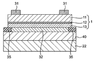
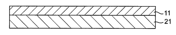
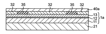
- FIG. 1 is a cross-sectional view showing the configuration of a nitride semiconductor element 1 according to the present embodiment arranged on the second substrate 22.
- the nitride semiconductor element 1 is arranged on the second substrate 22.
- the nitride semiconductor element 1 includes a p-side nitride semiconductor layer 13, an active layer 12, and an n-side nitride semiconductor layer 11 in this order from the second substrate 22 side.
- the first electrode 31 is electrically connected to the n-side nitride semiconductor layer 11.
- the second electrode 32 is electrically connected to the p-side nitride semiconductor layer 13.
- the nitride semiconductor element 1 is bonded to the second substrate 22 via the metal layer 40.
- the nitride semiconductor device 1 having such a structure can make the active layer 12 emit light by applying a voltage between the first electrode 31 and the second electrode 32.
- the light emitted by the nitride semiconductor element 1 is mainly emitted from the surface side of the n-side nitride semiconductor layer 11 where the first electrode 31 is provided.
- the nitride semiconductor device 1 of the present embodiment will be described in detail.
- the n-side nitride semiconductor layer 11 is, for example, a nitride semiconductor doped with n-type impurities such as Si.
- the n-side nitride semiconductor layer 11 may be composed of a single layer or may be composed of a plurality of layers. Further, the n-side nitride semiconductor layer 11 may include, for example, an undoped semiconductor layer as a part.
- the undoped semiconductor layer refers to a layer grown without adding n-type impurities when grown, and includes, for example, unavoidable impurities mixed from adjacent layers by diffusion or the like. You may.
- the p-side nitride semiconductor layer 13 is, for example, a nitride semiconductor doped with p-type impurities such as Mg.
- the p-side nitride semiconductor layer 13 may be composed of a single layer or may be composed of a plurality of layers. Further, the p-side nitride semiconductor layer 13 may include, for example, an undoped semiconductor layer as a part.
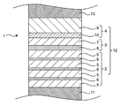
- the active layer 12 includes a plurality of well layers made of a nitride semiconductor and a plurality of barrier layers made of a nitride semiconductor.
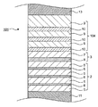
- the multiple quantum well structure according to the present embodiment is a first layer portion 2 including a plurality of first intermediate layers 6 and a plurality of barrier layers 5 in order from the n-side nitride semiconductor layer 11 side.
- the first layer portion 2 is a portion in which the first intermediate layer 6 and the barrier layer 5 are alternately laminated.
- a barrier layer 5 is arranged on the n-side nitride semiconductor layer 11, a first intermediate layer 6 is arranged on the barrier layer 5, and thereafter, the barrier layer 5 and the first intermediate layer 6 are alternately laminated.
- the barrier layer 5 is arranged at the top.
- the first layer portion 2 according to the present embodiment includes four barrier layers 5 and three first intermediate layers 6. As shown in FIG. 3, the barrier layer has a bandgap energy larger than that of the well layer. This also applies to the following second layer portion 3 and third layer portion 4.
- the barrier layer 5 is a nitride semiconductor layer containing Al, Ga, and N.
- the nitride semiconductor layer containing Al, Ga and N is, for example, a ternary compound.
- the general formula of the barrier layer 5 is, for example, Al a Ga 1-a N (0 ⁇ a ⁇ 1).
- the mixed crystal ratio of Al in the barrier layer 5 is preferably 0.05 ⁇ a ⁇ 0.15.
- the film thickness of the barrier layer 5 is, for example, 10 nm or more and 50 nm or less, preferably 20 nm or more and 40 nm.
- the barrier layer 5 of the first layer portion 2 may be doped with n-type impurities, similarly to the n-type impurity-doped barrier layer 7 of the second layer portion 3, which will be described later. Further, among the plurality of barrier layers 5, a part of the barrier layer 5 may be a barrier layer doped with n-type impurities, and the other part may be a barrier layer not doped with n-type impurities. By doping the barrier layer 5 of the first layer portion 2 with an n-type impurity, the recombination probability in the light emitting layer 10 is increased as in the case of the n-type impurity-doped barrier layer 7 of the second layer portion 3 described later. be able to.
- the first intermediate layer 6 is a nitride semiconductor layer containing Al, Ga, and N. As shown in FIG. 3, the first intermediate layer 6 has a bandgap energy larger than that of the second intermediate layer 8 and the light emitting layer 10.
- the first intermediate layer 6 is, for example, a ternary compound or a quaternary compound.
- Formula of the first intermediate layer 6 is, for example, Al b In c Ga 1-b -c N (0 ⁇ b ⁇ 1,0 ⁇ c ⁇ 1, b + c ⁇ 1).
- the mixed crystal ratio of Al in the first intermediate layer 6 is preferably 0.03 ⁇ b ⁇ 0.1.
- the In content of the first intermediate layer 6 is preferably 0 ⁇ c ⁇ 0.03.
- the first intermediate layer 6 By having the first intermediate layer 6 having such a composition, it is possible to suppress the absorption of light emitted from the light emitting layer 10.
- the first intermediate layer 6 is a non-luminous well layer that does not substantially emit light, unlike the light emitting layer 10.
- the film thickness of the first intermediate layer 6 is thinner than the film thickness of the second intermediate layer 8 and the light emitting layer 10. By having such a film thickness, self-absorption by the first intermediate layer 6 can be effectively suppressed.
- the film thickness of the first intermediate layer 6 is, for example, 2 nm or more and 10 nm or less, preferably 3 nm or more and 7 nm or less.
- the first intermediate layer 6 having the bandgap energy and the film thickness described above serves as a buffer layer for growing the light emitting layer 10 described later with good crystallinity, and also absorbs the light emitted from the light emitting layer 10. It can be suppressed.
- the second layer portion 3 is a portion in which one second intermediate layer 8 and one n-type impurity-doped barrier layer 7 are laminated.
- the second intermediate layer 8 is arranged on the barrier layer 5 laminated on the uppermost surface of the first layer portion 2, and the n-type impurity-doped barrier layer 7 is arranged on the second intermediate layer 8.
- the n-type impurity-doped barrier layer 7 in the second layer portion 3 is a nitride semiconductor layer containing Al, Ga, and N, which is doped with n-type impurities.
- the n-type impurity-doped barrier layer 7 is, for example, a ternary compound.
- the composition of the n-type impurity-doped barrier layer 7 may be the same as that of the barrier layer 5 described above.
- the film thickness of the n-type impurity-doped barrier layer 7 is, for example, 20 nm or more and 40 nm.
- the n-type impurity is, for example, Si.
- the concentration of n-type impurities in the n-type impurity-doped barrier layer 7 is, for example, 1 ⁇ 10 17 atoms / cm 3 or more and 1 ⁇ 10 19 atoms / cm 3 or less.
- the structure can be such that it does not emit light.
- the second intermediate layer 8 is a nitride semiconductor layer containing Ga and N, and is preferably a nitride semiconductor layer containing In, Ga and N. Further, as shown in FIG. 3, the second intermediate layer 8 has a bandgap energy smaller than that of the first intermediate layer 6.
- Formula of the second intermediate layer 8 is, for example, In d Ga 1-d N ( 0 ⁇ d ⁇ 1).
- the In content of the second intermediate layer 8 is preferably smaller than the In content of the light emitting layer 10.
- the bandgap energy of the second intermediate layer 8 can be made larger than the bandgap energy of the light emitting layer 10, and the light emitted from the light emitting layer 10 can be suppressed from being absorbed by the second intermediate layer 8.
- the In content of the second intermediate layer 8 is preferably 0 ⁇ d ⁇ 0.03.
- the second intermediate layer 8 is a non-luminous well layer that does not substantially emit light, unlike the light emitting layer 10 that emits light, like the first intermediate layer 6 described above.
- the bandgap energy of the second intermediate layer 8 is substantially the same as the bandgap energy of the light emitting layer 10, it is preferable that the film thickness of the second intermediate layer 8 is thinner than the film thickness of the light emitting layer 10. As a result, it is possible to prevent the light emitted from the light emitting layer 10 from being absorbed by the second intermediate layer 8. By reducing the film thickness of the second intermediate layer 8, self-absorption by the second intermediate layer 8 is suppressed.
- the film thickness of the second intermediate layer 8 is thicker than that of the first intermediate layer 6.
- the film thickness of the second intermediate layer 8 is, for example, 5 nm or more and 20 nm or less, preferably 10 nm or more and 18 nm or less.
- the second intermediate layer 8 having the bandgap energy and the film thickness described above suppresses the lattice relaxation of crystals generated between the first intermediate layer 6 and the light emitting layer 10 described later.
- lattice relaxation is a phenomenon in which strain is dispersed by generating dislocations at the boundary portions of crystals having different lattice constants, but on the other hand, dislocations occur due to lattice relaxation, which tends to reduce crystallinity. .. Therefore, in the nitride semiconductor device of the present embodiment, by providing the second intermediate layer 8, the crystallinity deteriorated by laminating the first intermediate layer 6 composed of the nitride semiconductor containing Al is restored. Can be done.
- the third layer portion 4 is a portion in which one light emitting layer 10 and one undoped barrier layer 9 are laminated.
- the light emitting layer 10 is arranged on the n-type impurity-doped barrier layer 7 of the second layer portion 3, and the undoped barrier layer 9 is arranged on the light emitting layer 10.
- the undoped barrier layer 9 in the third layer portion 4 is a nitride semiconductor layer that is not doped with n-type impurities.
- the undoped barrier layer 9 is, for example, a ternary compound.
- the undoped barrier layer 9 may have the same composition as the barrier layer 5 and the n-type impurity-doped barrier layer 7 described above.
- the film thickness of the undoped barrier layer 9 is thicker than that of the barrier layer 5 and the n-type impurity-doped barrier layer 7.
- the film thickness of the undoped barrier layer 9 is, for example, 30 nm or more and 50 nm or less.
- the undoped barrier layer 9 does not contain n-type impurities, the holes that have moved from the p-side nitride semiconductor layer 13 pass through the undoped barrier layer 9 and move to the light emitting layer 10. Therefore, the holes are efficiently supplied to the light emitting layer 10, and the luminous efficiency of the light emitting layer 10 is improved.
- the light emitting layer 10 is a nitride semiconductor layer containing Ga and N, and emits ultraviolet light.
- ultraviolet light means light having a wavelength of 400 nm or less.
- the general formula of the light emitting layer 10 is, for example, In e Ga 1-e N (0 ⁇ e ⁇ 1).
- the content of In is preferably 0 ⁇ e ⁇ 0.05.
- the light emitting layer 10 having such a composition emits ultraviolet light.
- the peak wavelength of the light emitted by the light emitting layer 10 is, for example, 365 nm or more and 400 nm or less. Examples of the peak wavelength of the light emitting layer 10 are about 365 nm and about 385 nm. Further, as shown in FIG.
- the light emitting layer 10 has, for example, substantially the same bandgap energy as the second intermediate layer 8.
- the peak wavelength of the light emitting layer 10 can be set to, for example, 250 nm or more and 365 nm or less.
- the Al content can be 0 ⁇ f ⁇ 0.6.
- the film thickness of the light emitting layer 10 is equal to or greater than the film thickness of the second intermediate layer 8.
- the film thickness of the light emitting layer 10 is, for example, 10 nm or more and 18 nm or less. The light emitting layer 10 having such a film thickness can promote the recombination of electrons and holes.
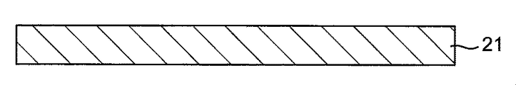
- the first substrate 21 made of sapphire is prepared.
- the n-type contact layer and the n-type clad layer are formed in order from the first substrate 21 side.
- the n-side nitride semiconductor layer 11 containing the mixture is formed.
- the n-side nitride semiconductor layer 11 may be formed on the first substrate 21 via a buffer layer.
- the active layer 12 is formed on the n-side nitride semiconductor layer 11.
- the active layer 12 is formed by the following steps.
- the barrier layer 5 is grown on the n-side nitride semiconductor layer 11 using a raw material gas containing an Al raw material gas, a Ga raw material gas, and an N raw material gas (barrier layer growth step).
- a raw material gas containing an Al raw material gas, a Ga raw material gas, and an N raw material gas barrier layer growth step.
- the composition of the barrier layer 5 is, for example, AlGaN
- the flow rate of the Al raw material gas is set in the range of 1 to 2 sccm
- the flow rate of the Ga raw material gas is set in the range of 30 to 50 sccm
- the flow rate of the N raw material gas is set.
- the barrier layer 5 can be formed by setting 5 to 10 slm.
- the first intermediate layer 6 is grown on the barrier layer 5 using the Al raw material gas, the In raw material gas, the Ga raw material gas, and the raw material gas containing the N raw material gas (first intermediate layer growth step).
- the composition of the first intermediate layer 6 is, for example, AlInGaN
- the flow rate of the Al raw material gas is set to 0.2 to 1.5 sccm
- the flow rate of the In raw material gas is set to the range of 0.1 to 25 sccm.
- the first intermediate layer 6 can be formed by setting the flow rate of the Ga raw material gas in the range of 30 to 50 sccm and setting the flow rate of the N raw material gas to 5 to 10 slm.
- the first layer portion 2 having a plurality of barrier layers 5 and the first intermediate layer 6 is formed.
- the step of forming the first layer portion 2 is completed in the barrier layer growth step.
- the second intermediate layer 8 is grown on the barrier layer 5 using the raw material gas containing the In raw material gas, the Ga raw material gas, and the N raw material gas (second intermediate layer growth step).
- the composition of the second intermediate layer 8 is, for example, InGaN
- the flow rate of the In raw material gas is set in the range of 0.1 to 25 sccm
- the flow rate of the Ga raw material gas is set in the range of 30 to 50 sccm
- N The second intermediate layer 8 can be formed by setting the flow rate of the raw material gas in the range of 5 to 10 slm.
- an n-type impurity-doped barrier layer 7 is grown on the second intermediate layer 8 using a raw material gas containing an Al raw material gas, a Ga raw material gas, an N raw material gas, and an n-type impurity raw material gas (n-type impurity). Dope barrier layer growth step).
- the composition of the n-type impurity-doped barrier layer 7 is, for example, AlGaN and the n-type impurity is Si
- the flow rate of the Al source gas is set in the range of 1 to 2 sccm
- the flow rate of the Ga source gas is 30 to 30 to.
- n-type impurities can be formed.
- the second layer portion 3 having the second intermediate layer 8 and the n-type impurity-doped barrier layer 7 is formed.
- the light emitting layer 10 is grown on the n-type impurity-doped barrier layer 7 using the raw material gas containing the In raw material gas, the Ga raw material gas, and the N raw material gas (light emitting layer growth step).
- the composition of the light emitting layer 10 is, for example, InGaN or GaN
- the flow rate of the In raw material gas is set in the range of 0 to 45 sccm
- the flow rate of the Ga raw material gas is set in the range of 30 to 50 sccm
- the flow rate of the Ga raw material gas is set in the range of 30 to 50 sccm.
- the light emitting layer 10 can be formed by setting the flow rate of the above in the range of 5 to 10 slm.
- the undoped barrier layer 9 is grown on the light emitting layer 10 using the raw material gas containing the Al raw material gas, the Ga raw material gas, and the N raw material gas (undoped barrier layer growth step).
- the composition of the undoped barrier layer 9 is, for example, AlGaN
- the flow rate of the Al raw material gas is set in the range of 1 to 2 sccm
- the flow rate of the Ga raw material gas is set in the range of 30 to 50 sccm
- the flow rate of the N raw material gas is set.
- the undoped barrier layer 9 can be formed by setting the flow rate in the range of 5 to 10 slm.
- the third layer portion 4 having the light emitting layer 10 and the undoped barrier layer 9 is formed.
- the p-side nitride semiconductor layer 13 including the p-type clad layer and the p-type contact layer is formed in this order.
- a semiconductor structure 1a having an n-side nitride semiconductor layer 11, an active layer 12, and a p-side nitride semiconductor layer 13 was formed on the first substrate 21.
- the first wafer 100 is prepared.
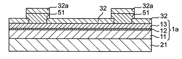
- a second electrode 32 having a predetermined pattern is formed on the p-side nitride semiconductor layer 13 of the first wafer 100 as follows, for example.
- the resist 51 is formed on the p-side nitride semiconductor layer 13 of the first wafer 100.
- the resist 51 is formed on the p-side nitride semiconductor layer 13 at a portion where the second electrode is not formed.
- a metal film (32, 32a) containing Ag is formed on the entire upper surface of the p-side nitride semiconductor layer 13.
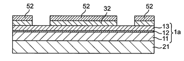
- the second electrode 32 is formed on the p-side nitride semiconductor layer 13 on which the resist 51 is not formed. Then, as shown in FIG. 10, the resist 51 is removed together with the metal film 32a formed on the resist 51. As described above, the second electrode 32 having a predetermined pattern is formed on the p-side nitride semiconductor layer 13 of the first wafer 100.
- a method of forming the second electrode 32 having a predetermined pattern by the lift-off process has been described. However, without using the lift-off process, for example, without forming the resist 51, a metal film is formed on the entire upper surface of the p-side nitride semiconductor layer 13, and a resist is formed on the metal film to form the resist.
- the second electrode 32 having a predetermined pattern may be formed by removing the metal film using the above as a mask.
- a resist 52 is formed on the second electrode 32.
- an insulating film 35a is formed on the portion of the p-side nitride semiconductor layer 13 on which the second electrode 32 is not formed and on the resist 52.
- the resist 52 is removed together with the insulating film 35a formed on the resist 52.
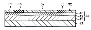
- the insulating film 35 is formed on the portion of the p-side nitride semiconductor layer 13 on which the second electrode 32 is not formed.
- the insulating film 35 is provided, for example, on the cutting position CL described later.
- the insulating film 35 can be configured so that the second electrode 32 is not exposed from the side surface of the light emitting device. As a result, the occurrence of a short circuit on the side surface of the light emitting device is suppressed, and the reliability can be improved.
- a metal layer 40a is formed on the second electrode 32 and the insulating film 35 formed on the p-side nitride semiconductor layer 13.
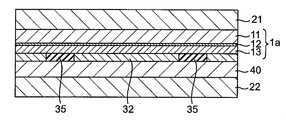
- a second substrate 22 having a metal layer 40b formed on one surface is prepared, and the metal layer 40b and the metal layer 40a are joined to each other.
- the second substrate 22 is bonded onto the p-side nitride semiconductor layer 13 via the second electrode 32 and the insulating film 35.
- the first substrate 21 is removed as shown in FIG.
- the second substrate 22 is bonded onto the p-side nitride semiconductor layer 13 of the first wafer 100, and the first substrate 21 of the first wafer 100 is removed.
- laser lift-off is performed by irradiating the vicinity of the interface between the first substrate 21 and the n-side nitride semiconductor layer 11 with a laser beam to separate the first substrate 21 and the n-side nitride semiconductor layer 11. To be done by. Alternatively, it is performed by performing wet etching to remove the first substrate 21 with a solution capable of etching.
- the semiconductor structure 1a formed on the first substrate 21 is transferred onto the second substrate 22 via the metal layer 40, the second electrode 32, and the insulating film 35.
- a second wafer 200 having a semiconductor structure 1a in which the n-side nitride semiconductor layer 11 is exposed on the surface is prepared on the second substrate 22. That is, in the second wafer 200, the p-side nitride semiconductor layer 13, the active layer 12, and the n-side nitride semiconductor layer are placed on the second substrate 22 via the metal layer 40, the second electrode 32, and the insulating film 35. 11 and 11 are laminated in order from the second substrate 22 side.
- the second substrate 22 is preferably a silicon substrate made of Si, and by using the second substrate 22 as a silicon substrate, the second substrate 22 can be easily divided in the cutting step described later. ..
- ⁇ Nitride semiconductor device separation process> a part of the semiconductor structure 1a of the second wafer 200 is removed to separate it into a plurality of nitride semiconductor elements 1.
- the semiconductor structure 1a is separated so as to correspond to each light emitting device obtained in the cutting step described later.
- Part of the semiconductor structure 1a is removed by dry etching such as reactive ion etching.
- the first electrode 31 having a predetermined pattern is formed on the n-side nitride semiconductor layer 11 of the second wafer 200 shown in FIG.
- the first electrode 31 can be formed by a lift-off process or an etching process using a resist in the same manner as the method for forming the second electrode 32 described above.
- the second wafer 200 on which the first electrode 31 is formed is divided into individual light emitting devices of a desired size. This division is performed along the predetermined cutting position CL shown in FIG. 19 by dicing or the like.
- the third layer portion 4 according to the nitride semiconductor element 1 of the above-described embodiment includes one light emitting layer 10 and one undoped barrier layer 9, but is not limited to this, and includes a plurality of light emitting layers 10.
- a plurality of undoped barrier layers 9 may be provided.
- the nitride semiconductor device 101 of one modification according to the present invention includes a third layer portion 104 including three light emitting layers 10 and three undoped barrier layers 9.
- the film thickness of the undoped barrier layer 9 provided in contact with the p-side nitride semiconductor layer 13 may be thicker than the film thickness of the other undoped barrier layers 9.
- the first layer portion 2 according to the nitride semiconductor element 1 described above includes the barrier layer 5 of four layers and the first intermediate layer 6 of three layers, but the first intermediate layer included in the first layer portion 2 is provided.
- the number of layers of 6 is not limited to this.
- the first layer portion 2 may include one first intermediate layer 6, or may include a plurality of first intermediate layers 6 having two layers or four or more layers.
- the number of layers of the barrier layer 5 may also differ depending on the number of layers of the first intermediate layer 6.
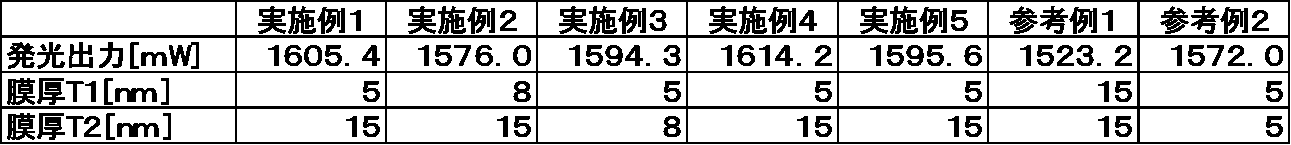
- Example 1 The nitride semiconductor device of Example 1 was manufactured as follows.
- a first substrate 21 made of sapphire is prepared, and an n-type contact layer and an n-type clad layer are grown on the first substrate 21, so that the n-type contact layer and the n-type clad layer are included in this order from the first substrate 21 side.
- the side nitride semiconductor layer 11 was formed.
- n-side nitride semiconductor layer 11 from Al 0.095 Ga 0.905 N, a barrier layer 5 containing n-type impurities, and Al 0.03 In 0.005 Ga 0.965 N.
- First intermediate layer 6 and the above-mentioned first intermediate layer 6 were laminated.
- three layers of the first intermediate layer 6 arranged between the four-layer barrier layer 5 and the four-layer barrier layer 5 are formed.
- the film thickness of the barrier layer 5 was grown to a thickness of 29 nm, and the thickness of the first intermediate layer 6 was grown to a thickness of 5 nm.
- the flow rate of each raw material gas when growing the barrier layer 5 was set to 1.5 sccm for Al raw material gas, 38.7 sccm for Ga raw material gas, and 7 slm for N raw material gas. Further, the n-type impurity contained in the barrier layer 5 was Si, and the doping amount of Si was set to be 1 ⁇ 10 18 atoms / cm 3.
- the flow rate of each raw material gas when growing the first intermediate layer 6 is set to 0.2 sccm for Al raw material gas, 6 sccm for In raw material gas, 43.6 sccm for Ga raw material gas, and N raw material. The gas was set to 7 slm.
- a second intermediate layer 8 composed of In 0.005 Ga 0.995 N and an n-type impurity composed of Al 0.095 Ga 0.905 N and containing Si as an n-type impurity are used.
- the dope barrier layer 7 and the dope barrier layer 7 were laminated one by one.
- the thickness of the second intermediate layer 8 was grown to a thickness of 15 nm, and the film thickness of the n-type impurity-doped barrier layer 7 was grown to a thickness of 29 nm.
- the flow rate of each raw material gas when growing the second intermediate layer 8 was set to 16 sccm for the In raw material gas, 43.6 sccm for the Ga raw material gas, and 7 slm for the N raw material gas.
- the flow rate of each raw material gas when growing the n-type impurity-doped barrier layer 7 was set to 1.5 sccm for the Al raw material gas, 38.7 sccm for the Ga raw material gas, and 7 slm for the N raw material gas. Further, the n-type impurity contained in the n-type impurity doping barrier layer 7 was Si, and the doping amount of Si was set to be 1 ⁇ 10 18 atoms / cm 3.
- one layer is a light emitting layer 10 made of In 0.005 Ga 0.995 N and an undoped barrier layer 9 made of Al 0.095 Ga 0.905 N. Stacked one by one.
- the thickness of the light emitting layer 10 was grown to 15 nm, and the film thickness of the undoped barrier layer 9 was grown to a thickness of 40 nm.
- the flow rate of each raw material gas when growing the light emitting layer 10 was set to 16 sccm for the In raw material gas, 43.6 sccm for the Ga raw material gas, and 7 slm for the N raw material gas.
- the flow rate of each raw material gas when growing the undoped barrier layer 9 was set to 1.5 sccm for the Al raw material gas, 38.7 sccm for the Ga raw material gas, and 7 slm for the N raw material gas.
- a p-side nitride semiconductor layer 13 including a p-type clad layer and a p-type contact layer was formed, and the first wafer 100 was prepared.
- a second electrode 32 having a predetermined pattern is formed on the p-side nitride semiconductor layer 13 of the first wafer 100, and is transferred to the second substrate 22 via the metal layer 40.
- the first substrate 21 was removed to form a first electrode 31 having a predetermined pattern on the n-side nitride semiconductor layer 11.
- the emission output of the nitride semiconductor device of Example 1 formed as described above when a current of 1000 mA was passed was evaluated. As a result, the emission output of the nitride semiconductor device of Example 1 was 1605.4 mW.
- Example 2 In the nitride semiconductor device of Example 1, the nitride semiconductor device of Example 2 was produced in the same manner as the nitride semiconductor device of Example 1 except that the thickness of the first intermediate layer 6 was grown to 8 nm. .. The light emitting output of the nitride semiconductor device of Example 2 produced as described above when a current of 1000 mA was passed was 1576.0 mW.
- Example 3 In the nitride semiconductor device of Example 1, the nitride semiconductor device of Example 3 was produced in the same manner as the nitride semiconductor device of Example 1 except that the thickness of the second intermediate layer 8 was grown to 8 nm. .. The light emitting output of the nitride semiconductor device of Example 3 produced as described above when a current of 1000 mA was passed was 1594.3 mW.
- Example 4 In the nitride semiconductor device of Example 1, the flow rate of the raw material gas when growing the first intermediate layer 6 is set to 0.4 sccm for the Al raw material gas, 6 sccm for the In raw material gas, and the Ga raw material gas.
- the nitride semiconductor device of Example 1 except that the N raw material gas was set to 43.6 sccm, the N raw material gas was set to 7 slm, and the composition of the first intermediate layer 6 was Al 0.045 In 0.005 Ga 0.95 N.
- the nitride semiconductor device of Example 4 was produced in the same manner as in the above.
- the light emitting output of the nitride semiconductor device of Example 4 produced as described above when a current of 1000 mA was passed was 1614.2 mW.
- Example 5 In the nitride semiconductor device of Example 1, the flow rate of the raw material gas when growing the first intermediate layer 6 is set to 0.6 sccm for the Al raw material gas, 6 sccm for the In raw material gas, and the Ga raw material gas.
- the nitride semiconductor device of Example 5 was produced in the same manner as in the above.
- the light emitting output of the nitride semiconductor device of Example 5 produced as described above when a current of 1000 mA was passed was 1595.6 mW.
- Reference example 1 In the nitride semiconductor device of Example 1, the same as that of the nitride semiconductor device of Example 1 except that the first intermediate layer 6 is composed of In 0.005 Ga 0.995 N and the film thickness is grown to 15 nm.
- the nitride semiconductor device of Reference Example 1 was manufactured.
- the flow rate of each raw material gas when growing the first intermediate layer 6 composed of In 0.005 Ga 0.995 N was set to 16 sccm for the In raw material gas and 43.6 sccm for the Ga raw material gas.
- the N raw material gas was set to 7 slm.
- the emission output of the nitride semiconductor device of Reference Example 1 produced as described above when a current of 1000 mA was passed was 1523.2 mW.
- the nitride semiconductor device of Example 1 In the nitride semiconductor device of Example 1, the nitride of Example 1 except that the second intermediate layer 8 is composed of Al 0.03 In 0.005 Ga 0.965 N and the film thickness is grown to 5 nm.
- the nitride semiconductor device of Reference Example 2 was manufactured in the same manner as the semiconductor device.
- the flow rate of each raw material gas when growing the second intermediate layer 8 composed of Al 0.03 In 0.005 Ga 0.965 N is set to 0.2 sccm for the Al raw material gas and 6 sccm for the In raw material gas.
- the Ga source gas was set to 43.6 sccm, and the N source gas was set to 7 slm.
- the emission output of the nitride semiconductor device of Reference Example 2 produced as described above when a current of 1000 mA was passed was 1572.0 mW.
- Example 1 The results of Examples 1 to 5 and Reference Examples 1 and 2 are shown in Table 1.
- Table 1 the film thickness of the first intermediate layer 6 is represented by the film thickness T1
- the film thickness of the second intermediate layer 8 is represented by the film thickness T2.
- the bandgap energy of the first intermediate layer 6 is larger than the bandgap energy of the second intermediate layer 8 and the bandgap energy of the light emitting layer 10, and the film thickness of the first intermediate layer 6 is the second.
- the nitride semiconductor devices of Examples 1 to 5 having a structure thinner than the film thickness of the intermediate layer 8 and the film thickness of the light emitting layer 10 may exhibit higher emission output than the nitride semiconductor devices of Reference Examples 1 and 2. It was revealed. Further, it was found that a high light emission output can be obtained by making the film thickness of the first intermediate layer 6 thinner. Furthermore, it was found that the luminescence output tends to decrease as the Al raw material gas when growing the first intermediate layer 6 is increased or decreased from a certain value.
- the nitride semiconductor device of Reference Example 1 in which the compositions of the first intermediate layer 6 and the second intermediate layer 8 were InGaN had a lower emission output than the nitride semiconductor devices of Examples 1 to 5. It is considered that this is because the self-absorption by the first intermediate layer 6 is generated more than the nitride semiconductor devices of Examples 1 to 5. Further, it was found that the nitride semiconductor device of Reference Example 2 in which the compositions of the first intermediate layer 6 and the second intermediate layer 8 were AlInGaN had a lower emission output than the nitride semiconductor devices of Examples 1 to 5. It is considered that this is due to the fact that the effect of suppressing the lattice relaxation by the second intermediate layer 8 is not obtained.
Landscapes
- Led Devices (AREA)
- Semiconductor Lasers (AREA)
Abstract
Description
n側窒化物半導体層と、
前記n側窒化物半導体層上に設けられ、窒化物半導体からなる複数の井戸層と、窒化物半導体からなる複数の障壁層とを備えた活性層と、
前記活性層上に設けられたp側窒化物半導体層と、を備え、
前記複数の井戸層は、前記n側窒化物半導体層側から順に、
前記障壁層よりも小さいバンドギャップを有し、AlとGaとNとを含む第1中間層と、
前記第1中間層より小さいバンドギャップエネルギーを有し、GaとNとを含む第2中間層と、
前記第1中間層より小さいバンドギャップエネルギーを有し、GaとNとを含む紫外光を発する発光層と、を有し、
前記第1中間層の膜厚は、前記第2中間層及び前記発光層の膜厚よりも薄く、
前記複数の障壁層のうち、前記第2中間層と前記発光層との間に配置される前記障壁層は、n型不純物がドープされている。
各図面中、同一の機能を有する部材には、同一符号を付している場合がある。要点の説明または理解の容易性を考慮して、便宜上実施形態や実施例に分けて示す場合があるが、異なる実施形態や実施例で示した構成の部分的な置換または組み合わせは可能である。後述の実施形態や実施例では、前述と共通の事柄についての記述を省略し、異なる点についてのみ説明する。特に、同様の構成による同様の作用効果については、実施形態や実施例ごとには逐次言及しないものとする。各図面が示す部材の大きさや位置関係等は、説明を明確にするため、誇張して示している場合もある。
そこで、本発明者は、窒化物半導体素子の発光出力に影響を及ぼす要素として、電子と正孔の再結合確率と、半導体層における結晶の格子緩和と、半導体層による光の自己吸収とに着目して鋭意検討を行った。
(1)第1中間層の膜厚を、第2中間層及び発光層の膜厚より薄くすることにより、発光層で発光した光の第1中間層における自己吸収をより効果的に抑えることができる。
(2)発光層と第2中間層の間の障壁層にn型不純物をドープすることにより発光層における再結合をより促進することができる。
また、第1中間層のバンドギャップエネルギーは、Al、Ga及びNを含む層とし、主としてAl、Ga及びNの組成比を調整することにより、発光層のバンドギャップエネルギーより大きくすることが好ましい。これにより、第1中間層による自己吸収を効果的に抑えることができる。
さらに第2中間層は、Ga及びNを含む層とし、主としてGa及びNの組成比を調整することにより、第1中間層のバンドギャップエネルギーより小さいバンドギャップエネルギーを有する。
以下、図面を参照しながら本実施形態の窒化物半導体素子とその窒化物半導体素子を備える発光装置の製造方法について説明する。
図1は、第2基板22上に配置された本実施形態に係る窒化物半導体素子1の構成を示す断面図である。
以下、本実施形態の窒化物半導体素子1について詳細に説明する。
n側窒化物半導体層11は、例えば、Si等のn型不純物をドープした窒化物半導体である。n側窒化物半導体層11は、単一の層で構成されていてもよいし、複数の層を含んで構成されていてもよい。また、n側窒化物半導体層11は、例えば、アンドープの半導体層を一部に含んでいてもよい。ここで、アンドープの半導体層とは、成長させるときにn型の不純物を添加することなく成長させた層のことをいい、例えば、隣接する層から拡散等により混入する不可避的な不純物を含んでいてもよい。
p側窒化物半導体層13は、例えば、Mg等のp型不純物をドープした窒化物半導体である。p側窒化物半導体層13は、単一の層で構成されていてもよいし、複数の層を含んで構成されていてもよい。また、p側窒化物半導体層13は、例えば、アンドープの半導体層を一部に含んでいてもよい。
活性層12は、窒化物半導体からなる複数の井戸層と、窒化物半導体からなる複数の障壁層とを備えている。本実施形態に係る多重量子井戸構造は、図2に示すように、n側窒化物半導体層11側から順に、複数の第1中間層6と複数の障壁層5とを含む第1層部2、第2中間層8とn型不純物ドープ障壁層7とを含む第2層部3、及び発光層10と不純物がドープされていないアンドープ障壁層9とを含む第3層部4を備えている。
第1層部2は、第1中間層6と障壁層5とが交互に積層されている部分である。n側窒化物半導体層11上には障壁層5が配置され、障壁層5の上に第1中間層6が配置されており、以降、障壁層5及び第1中間層6が交互に積層され、最も上には、障壁層5が配置されている。本実施形態に係る第1層部2は、4層の障壁層5と3層の第1中間層6とを備えている。なお、図3に示すように、障壁層は、井戸層よりも大きいバンドギャップエネルギーを有している。これは、以下の第2層部3及び第3層部4においても同様である。
第1中間層6の膜厚は、第2中間層8及び発光層10の膜厚よりも薄い。このような膜厚を有することで、第1中間層6による自己吸収を効果的に抑制できる。第1中間層6の膜厚は、例えば2nm以上10nm以下であり、好ましくは3nm以上7nm以下である。
上述したバンドギャップエネルギー及び膜厚を有する第1中間層6は、後述の発光層10を結晶性良く成長させるためのバッファ層としての役割を果たすとともに、発光層10から発光される光の吸収を抑制することができる。
第2層部3は、1つの第2中間層8と1つのn型不純物ドープ障壁層7とが積層されている部分である。第2中間層8は、第1層部2の最上に積層された障壁層5の上に配置されており、第2中間層8の上にn型不純物ドープ障壁層7が配置されている。
第2中間層8のバンドギャップエネルギーを発光層10のバンドギャップエネルギーとほぼ同じとする場合には、第2中間層8の膜厚を発光層10の膜厚よりも薄くすることが好ましい。これにより、発光層10から発光される光が第2中間層8により吸収されることを抑制できる。第2中間層8の膜厚を薄くすることにより第2中間層8による自己吸収が抑制される。第2中間層8の膜厚は、第1中間層6よりも厚い。第2中間層8の膜厚は、例えば5nm以上20nm以下であり、好ましくは10nm以上18nm以下である。
上述したバンドギャップエネルギー及び膜厚を有する第2中間層8は、第1中間層6と後述する発光層10との間に生じる結晶の格子緩和を抑制する。ここで、格子緩和は格子定数が異なる結晶の境界部分に転位を発生させることにより歪を分散させる現象であるが、一方で格子緩和が生じることで転位が発生し結晶性を低下させる傾向がある。そこで、本実施形態の窒化物半導体素子では、第2中間層8を設けることで、Alを含む窒化物半導体から構成された第1中間層6を積層することによって低下した結晶性を回復させることができる。
第3層部4は、1つの発光層10と1つのアンドープ障壁層9とが積層されている部分である。発光層10は、第2層部3のn型不純物ドープ障壁層7の上に配置されており、発光層10の上にアンドープ障壁層9が配置されている。
発光層10の膜厚は、第2中間層8の膜厚以上である。発光層10の膜厚は、例えば10nm以上18nm以下である。このような膜厚を有する発光層10は、電子と正孔の再結合を促進することができる。
次に、本実施形態の窒化物半導体素子を備える発光装置の製造方法について説明する。
第1ウエハ準備工程では、図4に示すように、例えば、サファイアからなる第1基板21を準備する。その後、図5に示すように、第1基板21上に、例えば、n型コンタクト層、n型クラッド層を成長させることにより、第1基板21側から順にn型コンタクト層、n型クラッド層を含むn側窒化物半導体層11を形成する。尚、第1基板21上にバッファ層を介してn側窒化物半導体層11を形成するようにしてもよい。
第2ウエハ準備工程では、まず、第1ウエハ100のp側窒化物半導体層13上に、所定のパターンの第2電極32を例えば以下のようにして形成する。
最初に、図8に示すように、第1ウエハ100のp側窒化物半導体層13上に、レジスト51を形成する。ここでは、例えば、p側窒化物半導体層13上の、第2電極を形成しない部分にレジスト51を形成する。
次に、図9に示すように、p側窒化物半導体層13の上面全体に、例えば、Agを含む金属膜(32、32a)を形成する。これにより、レジスト51が形成されていないp側窒化物半導体層13上に第2電極32が形成される。
そして、図10に示すように、レジスト51を、レジスト51上に形成された金属膜32aと共に除去する。
以上のようにして、第1ウエハ100のp側窒化物半導体層13上に、所定のパターンの第2電極32を形成する。
ここでは、リフトオフプロセスにより所定のパターンの第2電極32を形成する方法について説明した。しかしながら、リフトオフプロセスを用いることなく、例えば、レジスト51を形成することなくp側窒化物半導体層13の上面全体に、金属膜を形成して、その金属膜の上にレジストを形成してそのレジストをマスクとして金属膜を除去することにより、所定のパターンの第2電極32を形成するようにしてもよい。
次に、図18に示すように、第2ウエハ200の半導体構造1aの一部を除去することで複数の窒化物半導体素子1に分離する。この工程により、半導体構造1aは、後述する切断工程で得られるそれぞれの発光装置に対応するように分離される。半導体構造1aの一部の除去は、例えば、反応性イオンエッチングなどのドライエッチングにより行う。
次に、図19に示す第2ウエハ200のn側窒化物半導体層11上に、所定のパターンの第1電極31を形成する。第1電極31は、上述した第2電極32の形成方法と同様に、レジストを用いたリフトオフプロセスやエッチングプロセスにより形成することができる。
最後に、第1電極31が形成された第2ウエハ200を、所望の大きさの個々の発光装置に分割する。この分割は、ダイシングなどにより、図19に示す所定の切断位置CLに沿って行う。
以下、窒化物半導体素子1の変形例について説明する。
実施例1の窒化物半導体素子を以下のように作製した。
その結果、実施例1の窒化物半導体素子の発光出力は1605.4mWであった。
実施例1の窒化物半導体素子において、第1中間層6の膜厚を8nmに成長させた以外は、実施例1の窒化物半導体素子と同様にして実施例2の窒化物半導体素子を作製した。
以上のようにして作製した実施例2の窒化物半導体素子について1000mAの電流を流したときの発光出力は、1576.0mWであった。
実施例1の窒化物半導体素子において、第2中間層8の膜厚を8nmに成長させた以外は、実施例1の窒化物半導体素子と同様にして実施例3の窒化物半導体素子を作製した。
以上のようにして作製した実施例3の窒化物半導体素子について1000mAの電流を流したときの発光出力は、1594.3mWであった。
実施例1の窒化物半導体素子において、第1中間層6を成長させる際の原料ガスの流量について、Al原料ガスを0.4sccmに設定し、In原料ガスを6sccmに設定し、Ga原料ガスを43.6sccmに設定し、N原料ガスを7slmに設定し、第1中間層6の組成をAl0.045In0.005Ga0.95Nとした以外は、実施例1の窒化物半導体素子と同様にして実施例4の窒化物半導体素子を作製した。
以上のようにして作製した実施例4の窒化物半導体素子について1000mAの電流を流したときの発光出力は、1614.2mWであった。
実施例1の窒化物半導体素子において、第1中間層6を成長させる際の原料ガスの流量について、Al原料ガスを0.6sccmに設定し、In原料ガスを6sccmに設定し、Ga原料ガスを43.6sccmに設定し、N原料ガスを7slmに設定し、第1中間層6の組成をAl0.06In0.005Ga0.935Nとした以外は、実施例1の窒化物半導体素子と同様にして実施例5の窒化物半導体素子を作製した。
以上のようにして作製した実施例5の窒化物半導体素子について1000mAの電流を流したときの発光出力は、1595.6mWであった。
実施例1の窒化物半導体素子において、第1中間層6をIn0.005Ga0.995Nから構成し、膜厚を15nmに成長させた以外は、実施例1の窒化物半導体素子と同様にして参考例1の窒化物半導体素子を作製した。In0.005Ga0.995Nから構成された第1中間層6を成長させる際の各原料ガスの流量は、In原料ガスを16sccmに設定し、Ga原料ガスを43.6sccmに設定し、N原料ガスを7slmに設定した。
以上のようにして作製した参考例1の窒化物半導体素子について1000mAの電流を流したときの発光出力は、1523.2mWであった。
実施例1の窒化物半導体素子において、第2中間層8をAl0.03In0.005Ga0.965Nから構成し、膜厚を5nmに成長させた以外は、実施例1の窒化物半導体素子と同様にして参考例2の窒化物半導体素子を作製した。Al0.03In0.005Ga0.965Nから構成された第2中間層8を成長させる際の各原料ガスの流量は、Al原料ガスを0.2sccmに設定し、In原料ガスを6sccmに設定し、Ga原料ガスを43.6sccmに設定し、N原料ガスを7slmに設定した。
以上のようにして作製した参考例2の窒化物半導体素子について1000mAの電流を流したときの発光出力は、1572.0mWであった。
<表1>
第1中間層6及び第2中間層8の組成をInGaNとした参考例1の窒化物半導体素子は、実施例1~5の窒化物半導体素子よりも発光出力が低いことが分かった。これは、第1中間層6による自己吸収が実施例1~5の窒化物半導体素子よりも多く発生していることが影響していると考えられる。また第1中間層6及び第2中間層8の組成をAlInGaNとした参考例2の窒化物半導体素子は、実施例1~5の窒化物半導体素子よりも発光出力が低いことが分かった。これは、第2中間層8による格子緩和を抑制する効果が得られていないことが影響していると考えられる。
1a 半導体構造
2 第1層部
3 第2層部
4、104 第3層部
5 障壁層
6 第1中間層
7 n型不純物ドープ障壁層
8 第2中間層
9 アンドープ障壁層
10 発光層
11 n側窒化物半導体層
12 活性層
13 p側窒化物半導体層
21 第1基板
22 第2基板
31 第1電極
32 第2電極
35 絶縁膜
100 第1ウエハ
200 第2ウエハ
Claims (8)
- n側窒化物半導体層と、
前記n側窒化物半導体層上に設けられ、窒化物半導体からなる複数の井戸層と、窒化物半導体からなる複数の障壁層とを備えた活性層と、
前記活性層上に設けられたp側窒化物半導体層と、を備え、
前記複数の井戸層は、前記n側窒化物半導体層側から順に、
前記障壁層よりも小さいバンドギャップを有し、AlとGaとNとを含む第1中間層と、
前記第1中間層より小さいバンドギャップエネルギーを有し、GaとNとを含む第2中間層と、
前記第1中間層より小さいバンドギャップエネルギーを有し、GaとNとを含む紫外光を発する発光層と、を有し、
前記第1中間層の膜厚は、前記第2中間層及び前記発光層の膜厚よりも薄く、
前記複数の障壁層のうち、前記第2中間層と前記発光層との間に配置される前記障壁層は、n型不純物がドープされている、窒化物半導体素子。 - 前記複数の井戸層は、複数の前記第1中間層を備えることを特徴とする、請求項1に記載の窒化物半導体素子。
- 前記第2中間層のバンドギャップエネルギーは、前記発光層のバンドギャップエネルギーと略同じであり、
前記第2中間層の膜厚は、前記発光層の膜厚よりも薄いことを特徴とする、請求項1又は2に記載の窒化物半導体素子。 - 前記発光層及び前記第2中間層は、Inを含み、
前記第2中間層のInの含有量は、前記発光層のInの含有量よりも少ないことを特徴とする、請求項1~3のいずれか1項に記載の窒化物半導体素子。 - 前記第1中間層はAlGaNまたはAlInGaNであり、
前記第2中間層はGaNまたはInGaNであり、
前記発光層はGaNまたはInGaNであることを特徴とする、請求項1~4のいずれか1項に記載の窒化物半導体素子。 - 前記第1中間層の膜厚は3nm以上7nm以下であり、
前記第2中間層の膜厚は10nm以上18nm以下であり、
前記発光層の膜厚は10nm以上18nm以下であることを特徴とする、請求項1~5のいずれか1項に記載の窒化物半導体素子。 - 前記障壁層はAlとGaとNとを含むことを特徴とする、請求項1~6のいずれか1項に記載の窒化物半導体素子。
- 前記第2中間層と前記発光層との間に配置される前記障壁層の膜厚は20nm以上40nm以下であることを特徴とする、請求項1~7のいずれか1項に記載の窒化物半導体素子。
Priority Applications (4)
| Application Number | Priority Date | Filing Date | Title |
|---|---|---|---|
| JP2021561451A JP7469677B2 (ja) | 2019-11-26 | 2020-11-25 | 窒化物半導体素子 |
| CN202080080193.XA CN114730818B (zh) | 2019-11-26 | 2020-11-25 | 氮化物半导体元件 |
| US17/736,790 US20220271199A1 (en) | 2019-11-26 | 2022-05-04 | Nitride semiconductor element |
| JP2024007974A JP7659213B2 (ja) | 2019-11-26 | 2024-01-23 | 窒化物半導体素子 |
Applications Claiming Priority (4)
| Application Number | Priority Date | Filing Date | Title |
|---|---|---|---|
| JP2019213474 | 2019-11-26 | ||
| JP2019-213474 | 2019-11-26 | ||
| JP2020123823 | 2020-07-20 | ||
| JP2020-123823 | 2020-07-20 |
Related Child Applications (1)
| Application Number | Title | Priority Date | Filing Date |
|---|---|---|---|
| US17/736,790 Continuation US20220271199A1 (en) | 2019-11-26 | 2022-05-04 | Nitride semiconductor element |
Publications (1)
| Publication Number | Publication Date |
|---|---|
| WO2021106928A1 true WO2021106928A1 (ja) | 2021-06-03 |
Family
ID=76128695
Family Applications (1)
| Application Number | Title | Priority Date | Filing Date |
|---|---|---|---|
| PCT/JP2020/043810 Ceased WO2021106928A1 (ja) | 2019-11-26 | 2020-11-25 | 窒化物半導体素子 |
Country Status (4)
| Country | Link |
|---|---|
| US (1) | US20220271199A1 (ja) |
| JP (2) | JP7469677B2 (ja) |
| CN (1) | CN114730818B (ja) |
| WO (1) | WO2021106928A1 (ja) |
Cited By (1)
| Publication number | Priority date | Publication date | Assignee | Title |
|---|---|---|---|---|
| US12408490B2 (en) | 2022-02-16 | 2025-09-02 | Nichia Corporation | Light emitting element |
Citations (8)
| Publication number | Priority date | Publication date | Assignee | Title |
|---|---|---|---|---|
| WO2003103062A1 (en) * | 2002-06-04 | 2003-12-11 | Nitride Semiconductors Co.,Ltd. | Gallium nitride compound semiconductor device and manufacturing method |
| JP2008103711A (ja) * | 2006-10-20 | 2008-05-01 | Samsung Electronics Co Ltd | 半導体発光素子 |
| JP2010541223A (ja) * | 2007-09-26 | 2010-12-24 | オスラム オプト セミコンダクターズ ゲゼルシャフト ミット ベシュレンクテル ハフツング | 多重量子井戸構造を有するオプトエレクトロニクス半導体チップ |
| WO2011097150A1 (en) * | 2010-02-03 | 2011-08-11 | Cree, Inc. | Group iii nitride based light emitting diode structures with multiple quantum well structures having varying well thicknesses |
| JP2011198859A (ja) * | 2010-03-17 | 2011-10-06 | Toshiba Corp | 半導体発光素子、ウェーハ、半導体発光素子の製造方法及びウェーハの製造方法 |
| KR20120072568A (ko) * | 2010-12-24 | 2012-07-04 | 엘지디스플레이 주식회사 | 질화물 반도체 발광소자 |
| JP2013012684A (ja) * | 2011-06-30 | 2013-01-17 | Sharp Corp | 窒化物半導体発光素子 |
| JP2016219547A (ja) * | 2015-05-18 | 2016-12-22 | ローム株式会社 | 半導体発光素子 |
Family Cites Families (27)
| Publication number | Priority date | Publication date | Assignee | Title |
|---|---|---|---|---|
| JPH07170022A (ja) * | 1993-12-16 | 1995-07-04 | Mitsubishi Electric Corp | 半導体レーザ装置 |
| JP4629178B2 (ja) * | 1998-10-06 | 2011-02-09 | 日亜化学工業株式会社 | 窒化物半導体素子 |
| US6504171B1 (en) * | 2000-01-24 | 2003-01-07 | Lumileds Lighting, U.S., Llc | Chirped multi-well active region LED |
| JP3912043B2 (ja) * | 2001-04-25 | 2007-05-09 | 豊田合成株式会社 | Iii族窒化物系化合物半導体発光素子 |
| US6958497B2 (en) * | 2001-05-30 | 2005-10-25 | Cree, Inc. | Group III nitride based light emitting diode structures with a quantum well and superlattice, group III nitride based quantum well structures and group III nitride based superlattice structures |
| JP2006324685A (ja) * | 2002-07-08 | 2006-11-30 | Nichia Chem Ind Ltd | 窒化物半導体素子の製造方法及び窒化物半導体素子 |
| KR100649749B1 (ko) * | 2005-10-25 | 2006-11-27 | 삼성전기주식회사 | 질화물 반도체 발광 소자 |
| WO2011058682A1 (ja) * | 2009-11-12 | 2011-05-19 | パナソニック株式会社 | 窒化ガリウム系化合物半導体発光素子 |
| JP4960465B2 (ja) * | 2010-02-16 | 2012-06-27 | 株式会社東芝 | 半導体発光素子 |
| JP5671982B2 (ja) * | 2010-11-30 | 2015-02-18 | 三菱化学株式会社 | 半導体発光素子および半導体発光素子の製造方法 |
| JP5417307B2 (ja) * | 2010-12-02 | 2014-02-12 | 株式会社東芝 | 半導体発光素子 |
| US10134948B2 (en) * | 2011-02-25 | 2018-11-20 | Sensor Electronic Technology, Inc. | Light emitting diode with polarization control |
| JP5996846B2 (ja) * | 2011-06-30 | 2016-09-21 | シャープ株式会社 | 窒化物半導体発光素子およびその製造方法 |
| JP2013038394A (ja) * | 2011-07-14 | 2013-02-21 | Rohm Co Ltd | 半導体レーザ素子 |
| JP6005346B2 (ja) * | 2011-08-12 | 2016-10-12 | シャープ株式会社 | 窒化物半導体発光素子およびその製造方法 |
| JP5653327B2 (ja) * | 2011-09-15 | 2015-01-14 | 株式会社東芝 | 半導体発光素子、ウェーハ、半導体発光素子の製造方法及びウェーハの製造方法 |
| KR20130069157A (ko) * | 2011-12-16 | 2013-06-26 | 서울옵토디바이스주식회사 | 발광소자 |
| JP5468709B2 (ja) * | 2012-03-05 | 2014-04-09 | パナソニック株式会社 | 窒化物半導体発光素子、光源及びその製造方法 |
| US9318645B2 (en) * | 2012-10-19 | 2016-04-19 | Sharp Kabushiki Kaisha | Nitride semiconductor light-emitting element |
| US9124071B2 (en) * | 2012-11-27 | 2015-09-01 | Nichia Corporation | Nitride semiconductor laser element |
| JP5800252B2 (ja) * | 2013-03-25 | 2015-10-28 | ウシオ電機株式会社 | Led素子 |
| DE102013104351B4 (de) * | 2013-04-29 | 2022-01-20 | OSRAM Opto Semiconductors Gesellschaft mit beschränkter Haftung | Halbleiterschichtenfolge und Verfahren zum Betreiben eines optoelektronischen Halbleiterchips |
| JP2015177025A (ja) * | 2014-03-14 | 2015-10-05 | 株式会社東芝 | 光半導体素子 |
| KR102317473B1 (ko) * | 2015-03-19 | 2021-10-27 | 쑤저우 레킨 세미컨덕터 컴퍼니 리미티드 | 자외선 발광소자 및 조명시스템 |
| US9680056B1 (en) * | 2016-07-08 | 2017-06-13 | Bolb Inc. | Ultraviolet light-emitting device with a heavily doped strain-management interlayer |
| KR102006361B1 (ko) * | 2018-02-28 | 2019-08-02 | 주식회사 에스비케이머티리얼즈 | 자외선 발광 소자 |
| CN108321280B (zh) * | 2018-03-21 | 2024-11-19 | 华南理工大学 | 一种非极性紫外led及其制备方法 |
-
2020
- 2020-11-25 WO PCT/JP2020/043810 patent/WO2021106928A1/ja not_active Ceased
- 2020-11-25 CN CN202080080193.XA patent/CN114730818B/zh active Active
- 2020-11-25 JP JP2021561451A patent/JP7469677B2/ja active Active
-
2022
- 2022-05-04 US US17/736,790 patent/US20220271199A1/en active Pending
-
2024
- 2024-01-23 JP JP2024007974A patent/JP7659213B2/ja active Active
Patent Citations (8)
| Publication number | Priority date | Publication date | Assignee | Title |
|---|---|---|---|---|
| WO2003103062A1 (en) * | 2002-06-04 | 2003-12-11 | Nitride Semiconductors Co.,Ltd. | Gallium nitride compound semiconductor device and manufacturing method |
| JP2008103711A (ja) * | 2006-10-20 | 2008-05-01 | Samsung Electronics Co Ltd | 半導体発光素子 |
| JP2010541223A (ja) * | 2007-09-26 | 2010-12-24 | オスラム オプト セミコンダクターズ ゲゼルシャフト ミット ベシュレンクテル ハフツング | 多重量子井戸構造を有するオプトエレクトロニクス半導体チップ |
| WO2011097150A1 (en) * | 2010-02-03 | 2011-08-11 | Cree, Inc. | Group iii nitride based light emitting diode structures with multiple quantum well structures having varying well thicknesses |
| JP2011198859A (ja) * | 2010-03-17 | 2011-10-06 | Toshiba Corp | 半導体発光素子、ウェーハ、半導体発光素子の製造方法及びウェーハの製造方法 |
| KR20120072568A (ko) * | 2010-12-24 | 2012-07-04 | 엘지디스플레이 주식회사 | 질화물 반도체 발광소자 |
| JP2013012684A (ja) * | 2011-06-30 | 2013-01-17 | Sharp Corp | 窒化物半導体発光素子 |
| JP2016219547A (ja) * | 2015-05-18 | 2016-12-22 | ローム株式会社 | 半導体発光素子 |
Cited By (1)
| Publication number | Priority date | Publication date | Assignee | Title |
|---|---|---|---|---|
| US12408490B2 (en) | 2022-02-16 | 2025-09-02 | Nichia Corporation | Light emitting element |
Also Published As
| Publication number | Publication date |
|---|---|
| JP2024042006A (ja) | 2024-03-27 |
| CN114730818A (zh) | 2022-07-08 |
| JP7659213B2 (ja) | 2025-04-09 |
| CN114730818B (zh) | 2025-07-15 |
| US20220271199A1 (en) | 2022-08-25 |
| JPWO2021106928A1 (ja) | 2021-06-03 |
| JP7469677B2 (ja) | 2024-04-17 |
Similar Documents
| Publication | Publication Date | Title |
|---|---|---|
| JP6589987B2 (ja) | 窒化物半導体発光素子 | |
| JP5162016B1 (ja) | 半導体素子、ウェーハ、半導体素子の製造方法及びウェーハの製造方法 | |
| US8569738B2 (en) | Semiconductor light emitting device, wafer, method for manufacturing semiconductor light emitting device, and method for manufacturing wafer | |
| US7462876B2 (en) | Nitride semiconductor light emitting device | |
| JP4892618B2 (ja) | 半導体発光素子 | |
| JPWO2014061692A1 (ja) | 窒化物半導体発光素子 | |
| JP2013140966A (ja) | ストレイン緩衝層を用いて発光効率に優れた窒化物系発光素子 | |
| JP7659213B2 (ja) | 窒化物半導体素子 | |
| US12408484B2 (en) | Light emitting element and method of manufacturing light emitting element | |
| JP2022163904A (ja) | 半導体発光素子 | |
| JP7565028B2 (ja) | 発光素子の製造方法、及び発光素子の水素の抜き出し方法 | |
| JP7328558B2 (ja) | 発光素子及び発光素子の製造方法 | |
| JP5337862B2 (ja) | 半導体発光素子 | |
| KR100830643B1 (ko) | 발광 소자의 제조 방법 | |
| JP5554387B2 (ja) | 半導体発光素子 | |
| US12527126B2 (en) | Light-emitting element including p-side semiconductor layer having first, second, and third layers | |
| US20250107283A1 (en) | Light emitting element | |
| JP5787851B2 (ja) | 半導体素子、ウェーハ、半導体素子の製造方法及びウェーハの製造方法 | |
| JP5764184B2 (ja) | 半導体発光素子 | |
| JP2006339629A (ja) | 半導体素子 | |
| CN119133334A (zh) | 发光二极管及发光装置 |
Legal Events
| Date | Code | Title | Description |
|---|---|---|---|
| 121 | Ep: the epo has been informed by wipo that ep was designated in this application |
Ref document number: 20892253 Country of ref document: EP Kind code of ref document: A1 |
|
| ENP | Entry into the national phase |
Ref document number: 2021561451 Country of ref document: JP Kind code of ref document: A |
|
| NENP | Non-entry into the national phase |
Ref country code: DE |
|
| 122 | Ep: pct application non-entry in european phase |
Ref document number: 20892253 Country of ref document: EP Kind code of ref document: A1 |
|
| WWG | Wipo information: grant in national office |
Ref document number: 202080080193.X Country of ref document: CN |