WO2021107052A1 - コネクタ及び電子機器 - Google Patents
コネクタ及び電子機器 Download PDFInfo
- Publication number
- WO2021107052A1 WO2021107052A1 PCT/JP2020/044109 JP2020044109W WO2021107052A1 WO 2021107052 A1 WO2021107052 A1 WO 2021107052A1 JP 2020044109 W JP2020044109 W JP 2020044109W WO 2021107052 A1 WO2021107052 A1 WO 2021107052A1
- Authority
- WO
- WIPO (PCT)
- Prior art keywords
- insulator
- movable
- contact
- movable insulator
- connector
- Prior art date
- Legal status (The legal status is an assumption and is not a legal conclusion. Google has not performed a legal analysis and makes no representation as to the accuracy of the status listed.)
- Ceased
Links
Images


Classifications
-
- H—ELECTRICITY
- H01—ELECTRIC ELEMENTS
- H01R—ELECTRICALLY-CONDUCTIVE CONNECTIONS; STRUCTURAL ASSOCIATIONS OF A PLURALITY OF MUTUALLY-INSULATED ELECTRICAL CONNECTING ELEMENTS; COUPLING DEVICES; CURRENT COLLECTORS
- H01R12/00—Structural associations of a plurality of mutually-insulated electrical connecting elements, specially adapted for printed circuits, e.g. printed circuit boards [PCB], flat or ribbon cables, or like generally planar structures, e.g. terminal strips, terminal blocks; Coupling devices specially adapted for printed circuits, flat or ribbon cables, or like generally planar structures; Terminals specially adapted for contact with, or insertion into, printed circuits, flat or ribbon cables, or like generally planar structures
- H01R12/70—Coupling devices
- H01R12/71—Coupling devices for rigid printing circuits or like structures
- H01R12/72—Coupling devices for rigid printing circuits or like structures coupling with the edge of the rigid printed circuits or like structures
- H01R12/722—Coupling devices for rigid printing circuits or like structures coupling with the edge of the rigid printed circuits or like structures coupling devices mounted on the edge of the printed circuits
- H01R12/728—Coupling devices without an insulating housing provided on the edge of the PCB
-
- H—ELECTRICITY
- H01—ELECTRIC ELEMENTS
- H01R—ELECTRICALLY-CONDUCTIVE CONNECTIONS; STRUCTURAL ASSOCIATIONS OF A PLURALITY OF MUTUALLY-INSULATED ELECTRICAL CONNECTING ELEMENTS; COUPLING DEVICES; CURRENT COLLECTORS
- H01R12/00—Structural associations of a plurality of mutually-insulated electrical connecting elements, specially adapted for printed circuits, e.g. printed circuit boards [PCB], flat or ribbon cables, or like generally planar structures, e.g. terminal strips, terminal blocks; Coupling devices specially adapted for printed circuits, flat or ribbon cables, or like generally planar structures; Terminals specially adapted for contact with, or insertion into, printed circuits, flat or ribbon cables, or like generally planar structures
- H01R12/70—Coupling devices
- H01R12/91—Coupling devices allowing relative movement between coupling parts, e.g. floating or self aligning
-
- H—ELECTRICITY
- H01—ELECTRIC ELEMENTS
- H01R—ELECTRICALLY-CONDUCTIVE CONNECTIONS; STRUCTURAL ASSOCIATIONS OF A PLURALITY OF MUTUALLY-INSULATED ELECTRICAL CONNECTING ELEMENTS; COUPLING DEVICES; CURRENT COLLECTORS
- H01R12/00—Structural associations of a plurality of mutually-insulated electrical connecting elements, specially adapted for printed circuits, e.g. printed circuit boards [PCB], flat or ribbon cables, or like generally planar structures, e.g. terminal strips, terminal blocks; Coupling devices specially adapted for printed circuits, flat or ribbon cables, or like generally planar structures; Terminals specially adapted for contact with, or insertion into, printed circuits, flat or ribbon cables, or like generally planar structures
- H01R12/70—Coupling devices
- H01R12/71—Coupling devices for rigid printing circuits or like structures
- H01R12/712—Coupling devices for rigid printing circuits or like structures co-operating with the surface of the printed circuit or with a coupling device exclusively provided on the surface of the printed circuit
- H01R12/716—Coupling device provided on the PCB
-
- H—ELECTRICITY
- H01—ELECTRIC ELEMENTS
- H01R—ELECTRICALLY-CONDUCTIVE CONNECTIONS; STRUCTURAL ASSOCIATIONS OF A PLURALITY OF MUTUALLY-INSULATED ELECTRICAL CONNECTING ELEMENTS; COUPLING DEVICES; CURRENT COLLECTORS
- H01R13/00—Details of coupling devices of the kinds covered by groups H01R12/70 or H01R24/00 - H01R33/00
- H01R13/46—Bases; Cases
- H01R13/502—Bases; Cases composed of different pieces
-
- H—ELECTRICITY
- H01—ELECTRIC ELEMENTS
- H01R—ELECTRICALLY-CONDUCTIVE CONNECTIONS; STRUCTURAL ASSOCIATIONS OF A PLURALITY OF MUTUALLY-INSULATED ELECTRICAL CONNECTING ELEMENTS; COUPLING DEVICES; CURRENT COLLECTORS
- H01R12/00—Structural associations of a plurality of mutually-insulated electrical connecting elements, specially adapted for printed circuits, e.g. printed circuit boards [PCB], flat or ribbon cables, or like generally planar structures, e.g. terminal strips, terminal blocks; Coupling devices specially adapted for printed circuits, flat or ribbon cables, or like generally planar structures; Terminals specially adapted for contact with, or insertion into, printed circuits, flat or ribbon cables, or like generally planar structures
- H01R12/70—Coupling devices
- H01R12/71—Coupling devices for rigid printing circuits or like structures
- H01R12/72—Coupling devices for rigid printing circuits or like structures coupling with the edge of the rigid printed circuits or like structures
- H01R12/73—Coupling devices for rigid printing circuits or like structures coupling with the edge of the rigid printed circuits or like structures connecting to other rigid printed circuits or like structures
-
- H—ELECTRICITY
- H01—ELECTRIC ELEMENTS
- H01R—ELECTRICALLY-CONDUCTIVE CONNECTIONS; STRUCTURAL ASSOCIATIONS OF A PLURALITY OF MUTUALLY-INSULATED ELECTRICAL CONNECTING ELEMENTS; COUPLING DEVICES; CURRENT COLLECTORS
- H01R13/00—Details of coupling devices of the kinds covered by groups H01R12/70 or H01R24/00 - H01R33/00
- H01R13/46—Bases; Cases
- H01R13/514—Bases; Cases composed as a modular blocks or assembly, i.e. composed of co-operating parts provided with contact members or holding contact members between them
Definitions
- This disclosure relates to connectors and electronic devices.
- connection reliability for example, a part of the connector moves during and after fitting to absorb a misalignment between the connection object and the connector.
- a connector having a floating structure is known.
- Patent Document 1 discloses an electric connector having a floating structure and contributing to miniaturization while suppressing conduction failure due to flux rise.
- the connector according to the embodiment of the present disclosure is A fixed insulator formed in a frame shape, A movable insulator that is arranged inside the fixed insulator, is movable relative to the fixed insulator, and fits with the object to be connected. With the contacts attached to the fixed insulator and the movable insulator, With The movable insulator is arranged inside the fixed insulator in a state of being separated from each other, and has a first movable insulator and a second movable insulator that can move independently and separately.
- the electronic device according to the embodiment of the present disclosure is It has the above connector.
- FIG. 5 is an external perspective view showing a connector according to an embodiment in a state of being separated from a connection object in a top view.
- FIG. 5 is an external perspective view showing a single connector of FIG. 1 in a top view. It is a bottom view of the connector unit of FIG. It is an enlarged view which enlarged the broken line box V of FIG. It is an exploded perspective view of the connector of FIG. 3 from the top view. It is a cross-sectional perspective view along the arrow line VII-VII of FIG. It is an enlarged view of the broken line box VIII of FIG.
- FIG. 3 is an external perspective view showing a connection object connected to the connector of FIG. 3 from a top view. It is an exploded perspective view of the connection object of FIG. 12 from the top view. It is sectional drawing which follows the XIV-XIV arrow line of FIG. It is a schematic diagram which showed the 1st example in which a pair of contacts of FIG. 6 are elastically deformed. It is a schematic diagram which showed the 2nd example in which a pair of contacts of FIG. 6 are elastically deformed.
- FIG. 5 It is a front view which shows the 1st modification of the connector of FIG. It is an enlarged view corresponding to FIG. 5 which shows the 2nd modification of the connector of FIG. It is an enlarged view corresponding to FIG. 5 which shows the 3rd modification of the connector of FIG.
- connection object moves in the fitted state where the connection object and the connector are fitted, a load such as stress is generated on the movable insulator and the fixed insulator that are fitted with the connection target, and these The insulator is likely to be damaged or deformed.
- a load increases as the connector becomes longer due to, for example, multipolarization. Therefore, in a connector having a floating structure, a structure that suppresses such a load is required. In the electric connector described in Patent Document 1, a structure that suppresses such a load has not been sufficiently considered.
- the connector and the electronic device it is possible to suppress the load generated on the movable insulator and the fixed insulator fitted with the connection object in the connector having a floating structure.
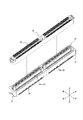
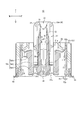
- FIG. 1 is an external perspective view showing a top view of the connector 10 according to the embodiment in which the connection object 60 is connected.
- FIG. 2 is an external perspective view showing the connector 10 according to the embodiment in a state of being separated from the connection object 60 in a top view.
- the connector 10 has a fixed insulator 20, a first movable insulator 30a, a second movable insulator 30b, a metal fitting 40, and a contact 50.
- movable insulator 30 when the first movable insulator 30a and the second movable insulator 30b are not collectively distinguished from each other, they are referred to as "movable insulator 30".
- the connector 10 will be described as a receptacle connector.
- the connection object 60 will be described as a plug connector.
- the connector 10 in which the contact 50 is elastically deformed in the fitted state in which the connector 10 and the connection object 60 are fitted to each other will be referred to as a receptacle connector, and the connection object 60 in which the contact 90 will not be elastically deformed will be described as a plug connector.
- the types of the connector 10 and the object to be connected 60 are not limited thereto.
- the connector 10 may serve as a plug connector
- the connection object 60 may serve as a receptacle connector.
- the connector 10 electrically connects the connection object 60 fitted with the connector 10 and the circuit board CB1, and electrically connects the circuit board CB2 on which the connection object 60 is mounted and the circuit board CB1.
- the circuit boards CB1 and CB2 may be rigid boards, or may be any other circuit boards.
- at least one of the circuit boards CB1 and CB2 may be a flexible printed circuit board (FPC).
- the connector 10 and the connection object 60 will be described as being connected to each other in the direction perpendicular to the circuit boards CB1 and CB2.
- the connector 10 and the object to be connected 60 are connected to each other in the vertical direction as an example.
- the connection method is not limited to this.
- the connector 10 and the object to be connected 60 may be connected to each other in a direction parallel to the circuit boards CB1 and CB2, or may be mounted so that one side is perpendicular to the mounted circuit board. They may be connected to each other so that the other is parallel to the circuit board.
- the “fitting direction” used in the following explanation means the vertical direction as an example.
- the “fitting side” means the upper side as an example.
- the “protruding direction” means the left-right direction as an example.
- the “arrangement direction of the contacts 50" means the left-right direction as an example.
- the connector 10 according to the embodiment has a floating structure.
- the connector 10 allows the connected object 60 to move relative to the circuit board CB1.
- the connection object 60 can move within a predetermined range with respect to the circuit board CB1 even when it is connected to the connector 10.
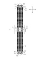
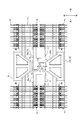
- FIG. 3 is an external perspective view showing the connector 10 unit of FIG. 1 in a top view.
- FIG. 4 is a bottom view of the connector 10 of FIG. 1 alone.
- FIG. 5 is an enlarged view of the broken line box V in FIG. 4.
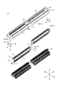
- FIG. 6 is an exploded perspective view of the connector 10 of FIG. 3 when viewed from above.
- FIG. 7 is a cross-sectional perspective view taken along the line VII-VII of FIG.
- FIG. 8 is an enlarged view of the broken line box VIII of FIG. 7.
- FIG. 9 is a cross-sectional view taken along the line VII-VII of FIG.
- FIG. 10 is a front view showing the pair of contacts 50 of FIG.
- FIG. 11 is an enlarged view of the broken line box XI of FIG.
- the VII-VII arrows are arranged on the first movable insulator 30a side as an example of the movable insulator 30, but the same cross section as in FIGS. 7 to 9 is on the second movable insulator 30b side. You can also get it. Therefore, the same contents as the following description regarding the first movable insulator 30a also apply to the second movable insulator 30b.
- the connector 10 is assembled by the following method as an example.
- the metal fitting 40 is press-fitted into the fixed insulator 20 from below, and the movable insulator 30 is arranged inside the fixed insulator 20 into which the metal fitting 40 is press-fitted.
- the contact 50 is press-fitted into the fixed insulator 20 and the movable insulator 30 from below.
- each component of the connector 10 in a state where the contact 50 is not elastically deformed will be mainly described.
- the configuration of the fixed insulator 20 will be mainly described with reference to FIGS. 3 to 9.
- the fixed insulator 20 is a square tubular member obtained by injection molding an insulating and heat resistant synthetic resin material.
- the fixed insulator 20 is formed in a frame shape and is hollow.
- the fixed insulator 20 has a first opening 21a and a second opening 21b on the upper surface.
- the fixed insulator 20 has a third opening 21c on the lower surface.
- the fixed insulator 20 includes four side walls in the front, rear, left and right, and has an outer peripheral wall 22 that surrounds the internal space. More specifically, the outer peripheral wall 22 is formed by a pair of short walls 22a on both the left and right sides and a pair of longitudinal walls 22b on both front and rear sides.
- the longitudinal wall 22b has protruding walls 22b1 formed so as to project inward in the front-rear direction at both left and right ends and in the center thereof.
- the fixed insulator 20 has a metal fitting mounting groove 23 recessed inside the fixed insulator 20 along the vertical direction on the short wall 22a.
- the metal fitting 40 is attached to the metal fitting mounting groove 23.
- the fixed insulator 20 has a plurality of contact mounting grooves 24 recessed from the lower edge portion to the lower surface and the inner surface inside the longitudinal wall 22b.
- the plurality of contact mounting grooves 24 are formed so as to be separated from each other at predetermined intervals along the left-right direction.
- the contact mounting groove 24 extends in the vertical direction on the longitudinal wall 22b of the fixed insulator 20.
- a contact 50 is attached to the contact attachment groove 24.
- the fixed insulator 20 has a partition wall 25 extending in the front-rear direction so as to connect the longitudinal walls 22b on both front and rear sides at the central portion of the longitudinal wall 22b.
- the partition wall 25 separates the first opening 21a and the second opening 21b along the left-right direction at the central portion of the longitudinal wall 22b.
- the partition wall 25 extends vertically along the inside of the fixed insulator 20 from the upper surface of the fixed insulator 20 to the central portion of the fixed insulator 20 in the vertical direction.
- the fixed insulator 20 has a pair of bosses 26 projecting from the left end of the rear longitudinal wall 22b and the lower surface of the right end of the front longitudinal wall 22b.
- the configuration of the movable insulator 30 will be described with reference mainly to FIGS. 4 to 9.
- the movable insulator 30 is arranged inside the fixed insulator 20 and can move relative to the fixed insulator 20.
- the movable insulator 30 fits with the object to be connected 60.
- the movable insulator 30 is arranged inside the fixed insulator 20 in a state of being separated from each other, and has a first movable insulator 30a and a second movable insulator 30b that can move independently and separately.
- the first movable insulator 30a and the second movable insulator 30b are formed so as to have the same shape as each other.
- the first movable insulator 30a and the second movable insulator 30b are arranged in a straight line along the arrangement direction of the contacts 50 in a state of being inverted with each other.
- the first movable insulator 30a is arranged on the left side of the movable insulator 30.
- the second movable insulator 30b is arranged on the right side of the movable insulator 30.
- first movable insulator 30a arranged on the left side along the arrangement direction of the contacts 50 will be focused on, and the configuration thereof will be mainly described.
- the same contents as the following description regarding the first movable insulator 30a also apply to the second movable insulator 30b.
- the first movable insulator 30a is a member that is injection-molded from an insulating and heat-resistant synthetic resin material and extends in the left-right direction.
- the first movable insulator 30a is formed in a convex shape when viewed from the front.
- the first movable insulator 30a has a bottom portion 31 that constitutes a lower portion, and a fitting convex portion 32 that projects upward from the bottom portion 31 and fits with the connection object 60.
- the bottom portion 31 is longer than the fitting convex portion 32 in the left-right direction.
- the bottom portion 31 has a protruding portion 31a that protrudes from the second movable insulator 30b side, that is, the right side surface toward the second movable insulator 30b.
- the protruding portion 31a has a facing surface 31b that is inclined obliquely with respect to the left-right direction.
- the first movable insulator 30a has a fitting recess 33 recessed in the upper surface of the fitting convex portion 32.
- the first movable insulator 30a has a guide portion 34 formed so as to surround the fitting recess 33 over the upper edge portion of the fitting convex portion 32.
- the invitation portion 34 is composed of an inclined surface that is inclined inward diagonally upward at the upper edge portion of the fitting convex portion 32.
- the first movable insulator 30a has a plurality of contact mounting grooves 35 formed in a state of being separated from each other at predetermined intervals along the left-right direction.
- the contact mounting groove 35 extends in the vertical direction.
- the lower portion of the contact mounting groove 35 is formed by recessing the lower portions of the front surface and the rear surface of the first movable insulator 30a.
- the central portion of the contact mounting groove 35 is formed inside the first movable insulator 30a.
- the upper portion of the contact mounting groove 35 is formed by recessing both inner surfaces of the fitting recess 33 in the front-rear direction.
- a contact 50 is attached to the contact attachment groove 35.
- the first movable insulator 30a has a wall portion 36 extending internally from the bottom surface of the fitting recess 33 downward.
- the wall portions 36 are located between a pair of contacts 50 attached to the first movable insulator 30a in a state of being arranged in the front-rear direction.
- the wall portion 36 faces the pair of contacts 50.
- the upper part of the wall portion 36 is formed to be the widest.
- the central portion of the wall portion 36 is formed to be narrower than the upper portion.
- the lower portion of the wall portion 36 is formed to be narrower than the central portion.
- the front and rear surfaces of the wall portion 36 form a part of the contact mounting groove 35.
- the central portion of the contact mounting groove 35 formed inside the first movable insulator 30a becomes narrower in the front-rear direction from the lower side to the upper side as the widths of the central portion and the upper portion of the wall portion 36 change. ..
- the first movable insulator 30a has a recess 37 that is recessed in the upper part of the fitting convex portion 32 over substantially the entire left-right direction.
- the concave portions 37 are formed on both front and rear sides in the upper portion of the fitting convex portion 32.
- the first movable insulator 30a has a pair of protrusions 38 protruding downward from the lower surfaces of the left and right ends of the bottom portion 31.
- the protruding portion 31a (first protruding portion) of the first movable insulator 30a protrudes from the side surface on the second movable insulator 30b side toward the second movable insulator 30b.
- the protruding portion 31a (second protruding portion) of the second movable insulator 30b is separated from the protruding portion 31a of the first movable insulator 30a, and protrudes from the side surface of the first movable insulator 30a toward the first movable insulator 30a.
- the tip of the protruding portion 31a of the first movable insulator 30a is located closer to the second movable insulator 30b than the tip of the protruding portion 31a of the second movable insulator 30b.
- the protruding portion 31a of the first movable insulator 30a and the protruding portion 31a of the second movable insulator 30b overlap each other along the protruding direction at least in part.
- the facing surface 31b of the first protruding portion and the facing surface 31b of the second protruding portion face each other along the front-rear direction.
- the two facing surfaces 31b are arranged substantially parallel to each other in a state of being inclined obliquely with respect to the left-right direction.
- the separation distance L1 along the front-rear direction of the two facing surfaces 31b is smaller than the separation distance L2 between the protrusion 31a and the protrusion 22b1 of the fixed insulator 20.
- the partition wall 25 of the fixed insulator 20 overlaps the first protruding portion and the second protruding portion from the fitting side between the connecting object 60 and the movable insulator 30. More specifically, the partition walls 25 of the fixed insulator 20 overlap each other along the projecting direction with respect to the overlapping portions of the first projecting portion and the second projecting portion from above.
- the configuration of the metal fitting 40 will be described with reference mainly to FIG.
- the metal fitting 40 is formed by molding a thin plate of an arbitrary metal material into the shape shown in FIG. 6 using a progressive remittance mold (stamping).
- the processing method of the metal fitting 40 includes a step of bending in the plate thickness direction after performing a punching process.
- the metal fitting 40 is press-fitted into the metal fitting mounting groove 23 of the fixed insulator 20, and is arranged at both left and right ends of the fixed insulator 20.
- the metal fitting 40 is formed in an H shape when viewed from the left and right directions.
- the metal fitting 40 has a mounting portion 41 extending outward in a U shape at the lower ends on both front and rear sides thereof.
- the metal fitting 40 has a connecting portion 42 extending in the front-rear direction at the central portion in the vertical direction thereof.
- the metal fitting 40 has a retaining portion 43 in the connecting portion 42 that projects inward from the lower edge portion of the central portion in the front-rear direction in the left-right direction.
- the retaining portion 43 suppresses the movable insulator 30 from coming out upward with respect to the fixed insulator 20.
- the metal fitting 40 has a locking portion 44 that locks to the metal fitting mounting groove 23 of the fixed insulator 20 at the upper end portions on both front and rear sides thereof.
- the configuration of the contact 50 will be described with reference mainly to FIGS. 9 to 11.
- the contact 50 has, for example, a thin plate of a copper alloy or Corson-based copper alloy having spring elasticity containing phosphor bronze, beryllium copper, or titanium copper, and has a shape shown in FIGS. 9 to 11 using a progressive mold (stamping). It is molded.
- the contact 50 is formed only by punching.
- the processing method of the contact 50 is not limited to this, and may include a step of bending in the plate thickness direction after performing the punching process.
- the contact 50 is formed of, for example, a metal material having a small elastic modulus so that the shape change due to elastic deformation becomes large.
- the surface of the contact 50 is plated with gold, tin, or the like after a base is formed by nickel plating.
- a plurality of contacts 50 are arranged along the left-right direction. As shown in FIG. 9, the contact 50 is attached to the fixed insulator 20 and the movable insulator 30. As shown in FIGS. 9 and 10, the pair of contacts 50 arranged at the same left and right positions are symmetrically formed and arranged along the front-rear direction. The pair of contacts 50 are formed and arranged so as to be line-symmetrical with each other with respect to the vertical axis passing through the center between them.
- the contact 50 has a base 51 that extends along the vertical direction and is supported by the fixed insulator 20.
- the contact 50 has a first locking portion 52a that is formed continuously from the lower end portion of the base portion 51 and engages with the contact mounting groove 24 of the fixed insulator 20.
- the contact 50 has a second locking portion 52b that is formed at the upper end of the base 51 and engages with the contact mounting groove 24 of the fixed insulator 20.
- the second locking portion 52b is formed on the fitting side with respect to the first wide portion 51a described later.
- the base portion 51, the first locking portion 52a, and the second locking portion 52b are housed in the contact mounting groove 24 of the fixed insulator 20.
- the contact 50 has a mounting portion 53 extending outward in an L shape from the outside of the lower end portion of the first locking portion 52a.
- the contact 50 forms a part of the base portion 51 and has a first wide portion 51a located on the fixed insulator 20 side.
- the first wide portion 51a is located inside the fixed insulator 20 along the inner surface of the longitudinal wall 22b.
- the first wide portion 51a is not directly locked to the fixed insulator 20, but is supported by the first locking portion 52a and the second locking portion 52b being locked to the fixed insulator 20.
- the first wide portion 51a is formed continuously with the first elastic portion 54a described later.
- the first wide portion 51a is formed so as to be adjacent to the first elastic portion 54a in the vicinity of the outer end portion of the first elastic portion 54a.
- the first wide portion 51a projects toward the movable insulator 30 in the front-rear direction with respect to other parts of the contact 50 along the fixed insulator 20.
- the first wide portion 51a projects one step inward in the front-rear direction with respect to the other portion of the base portion 51.
- the first wide portion 51a is wider in the front-rear direction than the other portions of the base 51.
- the first wide portion 51a is wider than the first elastic portion 54a.
- the first wide portion 51a is formed to have a larger cross-sectional area as a whole than the other portion of the base portion 51 and the first elastic portion 54a.
- the first wide portion 51a has higher electrical conductivity than the other portion of the base 51 and the first elastic portion 54a.
- the first wide portion 51a has a characteristic impedance lower than that of the other portion of the base 51 and the first elastic portion 54a.
- the contact 50 has an uneven portion 51b formed on the surface of the first wide portion 51a.
- the uneven portion 51b is formed as a convex portion.
- the uneven portion 51b is formed as a concave portion.
- the uneven portion 51b comes into contact with the surface of the contact mounting groove 24 in a state where the contact 50 is mounted on the fixed insulator 20.
- twisting of the contact 50 formed narrow in the left-right direction by the punching process along the left-right direction is suppressed. Therefore, the contact 50 is stably attached to the fixed insulator 20 even if the width is narrow in the left-right direction.
- the movable insulator 30 moves relative to the fixed insulator 20 in the fitted state in which the connector 10 and the object to be connected 60 are fitted, twisting of the contact 50 in the left-right direction is suppressed. Will be done.
- the contact 50 has a first elastic portion 54a that is elastically deformable and extends inward from the base portion 51 along the front-rear direction.
- the first elastic portion 54a extends inward from the base portion 51 diagonally downward, then bends diagonally upward, and extends linearly as it is.
- the first elastic portion 54a is bent downward again at the inner end portion thereof, and is connected to the upper end portion of the intermediate portion 54b described later.
- the first elastic portion 54a is formed to be narrower than the base portion 51 and the first wide portion 51a. As described above, the first elastic portion 54a can adjust the elastically displaced portion.
- the contact 50 has an intermediate portion 54b formed continuously with the first elastic portion 54a.
- the intermediate portion 54b has a wider electric conductivity than the first elastic portion 54a as a whole, that is, has a larger cross-sectional area than the first elastic portion 54a.
- the intermediate portion 54b extends in the fitting direction in a state where the contact 50 is not elastically deformed.
- the intermediate portion 54b includes a first adjusting portion 54b1 forming an upper portion, a second adjusting portion 54b2 forming a central portion, and a third adjusting portion 54b3 forming a lower portion.
- the upper end of the first adjusting portion 54b1 is connected to the first elastic portion 54a.
- the first adjusting portion 54b1 has a larger cross-sectional area than the first elastic portion 54a.
- the first adjusting portion 54b1 projects one step outward from the second adjusting portion 54b2 along the front-rear direction.
- the second adjusting portion 54b2 has a smaller cross-sectional area than the first adjusting portion 54b1 and a larger cross-sectional area than the first elastic portion 54a.
- the second adjusting portion 54b2 is formed to be narrower in the front-rear direction than the first adjusting portion 54b1 and wider in the front-rear direction than the first elastic portion 54a.
- the third adjusting portion 54b3 has a larger cross-sectional area than the second adjusting portion 54b2.
- the third adjusting portion 54b3 projects one step inward from the second adjusting portion 54b2 along the front-rear direction.
- the intermediate portion 54b has high electrical conductivity in the first adjusting portion 54b1 and the third adjusting portion 54b3, and has lower electrical conductivity in the second adjusting portion 54b2.
- the first adjusting portion 54b1 and the third adjusting portion 54b3 are formed symmetrically. More specifically, the first adjusting portion 54b1 and the third adjusting portion 54b3 are formed so as to be point-symmetrical with respect to the center of the intermediate portion 54b.
- the contact 50 has a second elastic portion 54c that is elastically deformable and extends from the lower end portion of the third adjustment portion 54b3 to the movable insulator 30.
- the second elastic portion 54c bends diagonally upward from the lower end portion of the third adjusting portion 54b3 and extends linearly as it is.
- the second elastic portion 54c is bent diagonally downward again and is connected to the outer end portion of the second wide portion 55, which will be described later.
- the second elastic portion 54c is formed to be narrower than the intermediate portion 54b like the first elastic portion 54a. As described above, the second elastic portion 54c can adjust the elastically displaced portion.
- the first elastic portion 54a, the intermediate portion 54b, and the second elastic portion 54c are integrally formed in a crank shape.
- the first elastic portion 54a, the intermediate portion 54b, and the second elastic portion 54c are arranged in order from the fitting side along the fitting direction.
- the first elastic portion 54a and the second elastic portion 54c are formed symmetrically with respect to the intermediate portion 54b. More specifically, the first elastic portion 54a and the second elastic portion 54c are formed so as to be point-symmetric with respect to the center of the intermediate portion 54b.
- the first elastic portion 54a and the second elastic portion 54c extend from both ends in the fitting direction in the intermediate portion 54b, respectively. More specifically, the first elastic portion 54a extends from the inner end portion of the upper edge portion of the first adjusting portion 54b1. On the other hand, the second elastic portion 54c extends from the outer end portion of the lower edge portion of the third adjusting portion 54b3. As described above, the connection point between the first elastic portion 54a and the intermediate portion 54b and the connection point between the second elastic portion 54c and the intermediate portion 54b are formed at positions symmetrical with respect to the center of the intermediate portion 54b. There is.
- the first elastic portion 54a and the second elastic portion 54c are continuous with the intermediate portion 54b at an end portion opposite to the end portion continuous with the first wide portion 51a and the second wide portion 55 described later. More specifically, the first elastic portion 54a is continuous with the first wide portion 51a at the outer end portion, while is continuous with the intermediate portion 54b at the inner end portion. Similarly, the second elastic portion 54c is continuous with the second wide portion 55 at the inner end portion, while is continuous with the intermediate portion 54b at the outer end portion.
- the contact 50 has a second wide portion 55 continuous with the second elastic portion 54c.
- the second wide portion 55 is formed so as to be adjacent to the second elastic portion 54c in the vicinity of the inner end portion of the second elastic portion 54c.
- the second wide portion 55 is located on the movable insulator 30 side.
- the second wide portion 55 is located in the contact mounting groove 35 of the movable insulator 30.
- the second wide portion 55 is not directly locked to the movable insulator 30, but is supported by locking the third locking portion 58, which will be described later, to the movable insulator 30.
- the second wide portion 55 projects toward the fixed insulator 20 in the front-rear direction with respect to other parts of the contact 50 along the movable insulator 30. More specifically, the second wide portion 55 projects one step outward in the front-rear direction from the third elastic portion 56, the third locking portion 58, and the elastic contact portion 59, which will be described later.
- the second wide portion 55 projects further toward the movable insulator 30 in the front-rear direction than other parts of the contact 50 along the movable insulator 30. More specifically, the second wide portion 55 projects further inward in the front-rear direction than the third elastic portion 56, which will be described later, over a wide area in the vertical direction.
- the second wide portion 55 is wider in the front-rear direction than the third elastic portion 56, the third locking portion 58, and the elastic contact portion 59. Similarly, the second wide portion 55 is wider than the second elastic portion 54c. As described above, the second wide portion 55 has a larger cross-sectional area than the second elastic portion 54c, the third elastic portion 56, the third locking portion 58, and the elastic contact portion 59 as a whole. As a result, the second wide portion 55 has higher electrical conductivity than the second elastic portion 54c, the third elastic portion 56, the third locking portion 58, and the elastic contact portion 59. More specifically, the second wide portion 55 has a lower characteristic impedance than the second elastic portion 54c, the third elastic portion 56, the third locking portion 58, and the elastic contact portion 59.
- the contact 50 has a third elastic portion 56 that is elastically deformable and extends upward from the second wide portion 55 and is arranged along the inner wall of the movable insulator 30.
- the third elastic portion 56 extends in the fitting direction in a state where it is not elastically deformed.
- the third elastic portion 56 faces the wall portion 36 of the movable insulator 30 formed inside the third elastic portion 56 as a whole.
- the contact 50 has a notch 57 formed on the surface of the third elastic portion 56 so as to form a bending point when the third elastic portion 56 elastically deforms.
- the cutout portion 57 is formed in a state in which the surface thereof is cut off at the central portion of the outer surface of the third elastic portion 56 in the front-rear direction.
- the contact 50 has a third locking portion 58 that is continuously formed above the third elastic portion 56 and engages with the movable insulator 30.
- the third locking portion 58 is formed wider than the third elastic portion 56.
- the contact 50 is continuously formed above the third locking portion 58 and has an elastic contact portion 59 that comes into contact with the contact 90 of the connection object 60 during fitting.
- the elastic contact portion 59 is formed at the tip of a portion of the contact 50 that is continuous from the second adjusting portion 54b2 to the opposite side of the first adjusting portion 54b1, for example.
- the second wide portion 55, the third elastic portion 56, the notch portion 57, and the third locking portion 58 are housed in the contact mounting groove 35 of the movable insulator 30.
- the second wide portion 55, the third elastic portion 56, and the third locking portion 58 face the wall portion 36 of the movable insulator 30 formed inside the second wide portion 55, the third elastic portion 56, and the third locking portion 58 substantially as a whole.
- the second wide portion 55 that connects the second elastic portion 54c and the third elastic portion 56 is arranged at a position facing the lower end portion of the wall portion 36.
- the lower half of the second wide portion 55 and the third elastic portion 56 is housed in the lower part of the contact mounting groove 35 formed as recessed portions on the front and rear surfaces of the movable insulator 30.
- the upper half of the third elastic portion 56 and the third locking portion 58 are housed in the central portion of the contact mounting groove 35 formed inside the movable insulator 30.
- the notch 57 is formed on the surface of the third elastic portion 56 so as to be located near the boundary between the lower portion and the central portion of the contact mounting groove 35.
- the elastic contact portion 59 is located above the contact mounting groove 35 formed as a recessed portion on the inner surface of the fitting recess 33 of the movable insulator 30. The tip of the elastic contact portion 59 is exposed from the contact mounting groove 35 into the fitting recess 33.
- the connector 10 having the above structure is positioned with respect to the circuit board CB1 by engaging the boss 26 of the fixed insulator 20 with an arbitrary recess formed in the circuit board CB1, for example.
- the mounting portion 53 of the contact 50 is soldered to the circuit pattern formed on the mounting surface of the circuit board CB1.
- the mounting portion 41 of the metal fitting 40 is soldered to the pattern formed on the mounting surface.
- the connector 10 is mounted on the circuit board CB1.
- an electronic component other than the connector 10 such as a CPU (Central Processing Unit), a controller, or a memory is mounted.
- each of the plurality of contacts 50 attached to one movable insulator 30 can be arbitrarily used for signals, power supply, or grounding with respect to the circuit pattern formed on the mounting surface of the circuit board CB1. It may be assigned by the combination of. For example, among the plurality of contacts 50, the mounting portion 53 of some of the contacts 50 is assigned for signals, the other mounting portion 53 is assigned for power supply, and the other mounting portion 53 is grounded. May be assigned for.
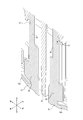
- connection object 60 The structure of the connection object 60 will be described mainly with reference to FIGS. 12 and 13.
- FIG. 12 is an external perspective view showing a connection object 60 connected to the connector 10 of FIG. 3 from a top view.
- FIG. 13 is an exploded perspective view of the connection object 60 of FIG. 12 when viewed from above.
- connection object 60 has an insulator 70, a metal fitting 80, and a contact 90 as major components.
- the connection object 60 is assembled by press-fitting the metal fitting 80 into the insulator 70 from above and pressing the contact 90 from below.
- the insulator 70 is a square columnar member obtained by injection molding an insulating and heat resistant synthetic resin material.
- the insulator 70 has a first fitting recess 71 and a second fitting recess 72 formed on the upper surface and arranged linearly along the left-right direction.
- the insulator 70 has a first fitting convex portion 73 formed inside the first fitting concave portion 71.
- the insulator 70 has a second fitting convex portion 74 formed inside the second fitting concave portion 72.
- the insulator 70 has a lead-in portion 75 formed so as to surround the upper edges of the first fitting recess 71 and the second fitting recess 72, respectively.
- the lead-in portion 75 is composed of an inclined surface that is inclined outward at an upper edge portion of the first fitting recess 71 and the second fitting recess 72.
- the insulator 70 has a metal fitting mounting groove 76 projecting from the left and right side surfaces to the outside in the left-right direction.
- the metal fitting 80 is attached to the metal fitting mounting groove 76.
- the insulator 70 has a plurality of contact mounting grooves 77 formed on both front and rear sides of the bottom portion and on the front and rear surfaces of the first fitting convex portion 73 and the second fitting convex portion 74.
- a plurality of contacts 90 are attached to the plurality of contact mounting grooves 77, respectively.
- the plurality of contact mounting grooves 77 are formed so as to be separated from each other at predetermined intervals along the left-right direction.
- the metal fitting 80 is formed by molding a thin plate of an arbitrary metal material into the shape shown in FIG. 13 using a progressive remittance mold (stamping).
- the metal fittings 80 are arranged at the left and right ends of the insulator 70, respectively.
- the metal fitting 80 has a mounting portion 81 extending outward in an L shape at the lower end portion thereof.
- the metal fitting 80 is formed continuously above the mounting portion 81 and has a locking portion 82 that locks to the metal fitting mounting groove 76 of the insulator 70.
- the contact 90 was formed by molding a thin plate of a copper alloy having spring elasticity containing phosphor bronze, beryllium copper, or titanium copper or a Corson-based copper alloy into the shape shown in FIG. 13 using a progressive mold (stamping). It is a thing.
- the surface of the contact 90 is plated with gold, tin, or the like after a base is formed by nickel plating.
- a plurality of contacts 90 are arranged along the left-right direction.
- the contact 90 has a mounting portion 91 extending outward in an L shape.
- the contact 90 has a contact portion 92 formed at the upper end thereof and in contact with the elastic contact portion 59 of the contact 50 in a fitted state in which the connection object 60 and the connector 10 are fitted.
- connection object 60 having the above structure, the mounting portion 91 of the contact 90 is soldered to the circuit pattern formed on the mounting surface of the circuit board CB2.
- the mounting portion 81 of the metal fitting 80 is soldered to the pattern formed on the mounting surface.
- the connection object 60 is mounted on the circuit board CB2.
- an electronic component different from the connection object 60 including a camera module, a sensor, and the like is mounted.
- each of the plurality of contacts 90 may be assigned to the circuit pattern formed on the mounting surface of the circuit board CB2 in any combination of signal, power supply, and grounding.
- the mounting unit 91 of some of the contacts 90 is assigned for signals
- the other mounting parts 91 are assigned for power supply
- the other mounting parts 91 are grounded. May be assigned for.
- FIG. 14 is a cross-sectional view taken along the XIV-XIV arrow line of FIG.
- the XIV-XIV arrow line is arranged on the first movable insulator 30a side as an example of the movable insulator 30, but the same cross section as in FIG. 14 is also arranged on the second movable insulator 30b side. can get. Therefore, the same contents as the following description regarding the first movable insulator 30a also apply to the second movable insulator 30b.
- the operation of the connector 10 having a floating structure will be described with reference mainly to FIG.
- the contact 50 of the connector 10 supports the first movable insulator 30a in a state in which the first movable insulator 30a is separated from the fixed insulator 20 and is floating inside the fixed insulator 20. At this time, the lower portion of the first movable insulator 30a is surrounded by the outer peripheral wall 22 of the fixed insulator 20. The upper portion of the first movable insulator 30a including the fitting recess 33 projects upward from the first opening 21a of the fixed insulator 20.
- the fixed insulator 20 is fixed to the circuit board CB1 by soldering the mounting portion 53 of the contact 50 to the circuit board CB1.
- the first movable insulator 30a can move with respect to the fixed insulator 20 fixed to the circuit board CB1 by elastically deforming the first elastic portion 54a, the second elastic portion 54c, and the third elastic portion 56 of the contact 50. It becomes.
- the protruding wall 22b1 of the longitudinal wall 22b of the fixed insulator 20 regulates the excessive movement of the first movable insulator 30a with respect to the fixed insulator 20 in the front-rear direction.
- the bottom portion 31 or the protruding portion 31a of the first movable insulator 30a comes into contact with the protrusion 22b1.
- the left end of the bottom 31 of the first movable insulator 30a comes into contact with the leftmost protruding wall 22b1 of the longitudinal wall 22b.
- the protruding portion 31a of the first movable insulator 30a comes into contact with the central protruding wall 22b1 of the longitudinal wall 22b. As a result, the first movable insulator 30a does not move further outward in the front-rear direction.
- the short wall 22a and the partition wall 25 of the fixed insulator 20 regulate the excessive movement of the first movable insulator 30a with respect to the fixed insulator 20 in the left-right direction.
- the fitting convex portion 32 of the first movable insulator 30a comes into contact with the short wall 22a or the partition wall 25.
- the first movable insulator 30a does not move further outward in the left-right direction.
- the protrusion 38 of the first movable insulator 30a regulates the excessive downward movement of the first movable insulator 30a with respect to the fixed insulator 20. For example, when the first movable insulator 30a moves significantly downward beyond the design value due to the elastic deformation of the contact 50, the protrusion 38 of the first movable insulator 30a comes into contact with the surface of the circuit board CB1. As a result, the first movable insulator 30a does not move further downward.
- the front-rear position and the left-right position of the connector 10 and the connection object 60 are substantially aligned with each other. Face each other in the vertical direction. After that, the object to be connected 60 is moved downward. At this time, even if the positions are slightly deviated from each other in the front-back and left-right directions, for example, the invitation portion 34 of the connector 10 and the invitation portion 75 of the connection object 60 come into contact with each other. As a result, the first movable insulator 30a and the second movable insulator 30b move relative to the fixed insulator 20 due to the floating structure of the connector 10.
- the fitting convex portion 32 of the first movable insulator 30a is attracted to the first fitting concave portion 71 of the insulator 70.
- the fitting convex portion 32 of the second movable insulator 30b is attracted to the second fitting concave portion 72 of the insulator 70.
- the fitting convex portion 32 of the first movable insulator 30a and the first fitting concave portion 71 of the insulator 70 are fitted to each other.
- the fitting convex portion 32 of the second movable insulator 30b and the second fitting concave portion 72 of the insulator 70 are fitted to each other.
- the fitting recess 33 of the first movable insulator 30a and the first fitting convex portion 73 of the insulator 70 are fitted to each other.
- the fitting recess 33 of the second movable insulator 30b and the second fitting convex portion 74 of the insulator 70 are fitted to each other.
- the contact 50 of the connector 10 and the contact 90 of the connection target 60 come into contact with each other. More specifically, the elastic contact portion 59 of the contact 50 and the contact portion 92 of the contact 90 come into contact with each other. At this time, the tip of the elastic contact portion 59 of the contact 50 is slightly elastically deformed toward the outside and elastically displaced toward the inside of the contact mounting groove 35.
- the connector 10 and the connection object 60 are completely connected.
- the circuit board CB1 and the circuit board CB2 are electrically connected via the contact 50 and the contact 90.
- the pair of elastic contact portions 59 of the contact 50 sandwich the pair of contacts 90 of the connection object 60 from both front and rear sides by an inward elastic force along the front-rear direction.
- the movable insulator 30 exerts a force in the removal direction, that is, upward direction through the contact 50. receive.
- the partition wall 25 of the fixed insulator 20 and the retaining portion 43 of the metal fitting 40 press-fitted into the fixed insulator 20 suppress the movable insulator 30 from coming out upward.
- the partition wall 25 of the fixed insulator 20 is located directly above the protruding portion 31a of the movable insulator 30 arranged inside the fixed insulator 20.
- the retaining portion 43 of the metal fitting 40 press-fitted into the fixed insulator 20 is located inside the fixed insulator 20 directly above the left and right ends of the bottom portion 31 of the movable insulator 30. Therefore, when the movable insulator 30 tries to move upward, the protruding portion 31a comes into contact with the partition wall 25, and the left and right end portions of the bottom portion 31 protruding outward come into contact with the retaining portion 43. As a result, the movable insulator 30 does not move further upward.
- FIG. 15 is a schematic view showing a first example in which the pair of contacts 50 of FIG. 6 are elastically deformed.
- FIG. 16 is a schematic view showing a second example in which the pair of contacts 50 of FIG. 6 are elastically deformed.
- each component when the pair of contacts 50 are elastically deformed will be described in detail.
- the contact 50 arranged on the right side of each drawing will be referred to as a contact 50a
- the contact 50 arranged on the left side of each drawing will be referred to as a contact 50b.
- the state in which the contacts 50a and 50b are not elastically deformed is shown by a chain double-dashed line.
- the third locking portion 58 of the contact 50a is pushed to the right by the wall portion 36 of the movable insulator 30.
- the third elastic portion 56 of the contact 50a bends inward starting from the vicinity of the notch portion 57.
- the third elastic portion 56 of the contact 50a is elastically deformed more inward than the upper portion on the lower side than the vicinity of the notch portion 57.
- the third locking portion 58 of the contact 50a which is in contact with the wall portion 36 of the movable insulator 30, hardly changes the relative position with the movable insulator 30.
- the second wide portion 55 of the contact 50a changes its relative position inward.
- the second elastic portion 54c is elastically deformed, and the connection point between the second elastic portion 54c and the intermediate portion 54b also moves to the right.
- the change in the left-right position of the connection point between the first elastic portion 54a and the intermediate portion 54b is small. Therefore, the first elastic portion 54a is elastically deformed, the bent portion at the inner end portion thereof is bent outward, and the intermediate portion 54b is inclined obliquely to the right from the upper side to the lower side.
- the third locking portion 58 of the contact 50b is pushed to the right by the inner wall of the movable insulator 30.
- the third elastic portion 56 of the contact 50b bends outward starting from the vicinity of the notch portion 57.
- the third elastic portion 56 of the contact 50b is elastically deformed to the outer side as compared with the upper portion on the lower side than the vicinity of the notch portion 57.
- the third locking portion 58 of the contact 50b which is in contact with the inner wall of the contact mounting groove 35, hardly changes the relative position with the movable insulator 30.
- the second wide portion 55 of the contact 50b changes its relative position outward.
- the second elastic portion 54c is elastically deformed, and the connection point between the second elastic portion 54c and the intermediate portion 54b also moves to the right.
- the change in the left-right position of the connection point between the first elastic portion 54a and the intermediate portion 54b is small. Therefore, the first elastic portion 54a is elastically deformed, the bent portion at the inner end portion thereof is bent inward, and the intermediate portion 54b is inclined diagonally to the right from the upper side to the lower side.
- the third locking portion 58 of the contact 50a is pushed to the left by the inner wall of the movable insulator 30.
- the third elastic portion 56 of the contact 50a bends outward starting from the vicinity of the notch portion 57.
- the third elastic portion 56 of the contact 50a is elastically deformed to the outer side as compared with the upper portion on the lower side than the vicinity of the notch portion 57.
- the third locking portion 58 of the contact 50a which is in contact with the inner wall of the contact mounting groove 35, hardly changes the relative position with the movable insulator 30.
- the second wide portion 55 of the contact 50a changes its relative position outward.
- the connection point between the second elastic portion 54c and the intermediate portion 54b also moves to the left while the second elastic portion 54c is elastically deformed.
- the change in the left-right position of the connection point between the first elastic portion 54a and the intermediate portion 54b is small. Therefore, the first elastic portion 54a is elastically deformed, the bent portion at the inner end portion thereof is bent inward, and the intermediate portion 54b is inclined diagonally to the left from the upper side to the lower side.
- the third locking portion 58 of the contact 50b is pushed to the left by the wall portion 36 of the movable insulator 30.
- the third elastic portion 56 of the contact 50b bends inward starting from the vicinity of the notch portion 57.
- the third elastic portion 56 of the contact 50b is elastically deformed more inward than the upper portion on the lower side than the vicinity of the notch portion 57.
- the third locking portion 58 of the contact 50b which is in contact with the wall portion 36 of the movable insulator 30, hardly changes the relative position with the movable insulator 30.
- the second wide portion 55 of the contact 50b changes its relative position inward.
- connection point between the second elastic portion 54c and the intermediate portion 54b also moves to the left while the second elastic portion 54c is elastically deformed.
- the change in the left-right position of the connection point between the first elastic portion 54a and the intermediate portion 54b is small. Therefore, the first elastic portion 54a is elastically deformed, the bent portion at the inner end portion thereof is bent outward, and the intermediate portion 54b is inclined obliquely to the left from the upper side to the lower side.
- the connector 10 has a floating structure, and can suppress the load generated on the movable insulator 30 and the fixed insulator 20 that are fitted to the connection object 60. As a result, the connector 10 can suppress damage or deformation of these insulators.
- the movable insulator 30 has a first movable insulator 30a and a second movable insulator 30b separated from each other. As a result, even if the connection object 60 moves in the fitted state where the connection object 60 and the connector 10 are fitted, the load such as stress on the movable insulator 30 fitted with the connection target 60 is suppressed. To.
- the movable insulator 30 has a first movable insulator 30a and a second movable insulator 30b separated from each other.
- the movable insulator 30 can be moved individually by separating the movable insulator 30 into two, the movable insulator 30 can be moved as compared with the case where the movable insulator 30 is integrated. Sex improves. Therefore, it becomes easy to lure the first fitting recess 71 and the second fitting recess 72 of the connection object 60 between the movable insulator 30 and the movable insulator 30, and a good floating structure can be realized in the connector 10. The work of inserting the connection object 60 into the connector 10 becomes easy.
- the partition wall 25 of the fixed insulator 20 overlaps with the protrusion 31a of the movable insulator 30 from the fitting side, and when the movable insulator 30 tries to move upward, the protrusion 31a comes into contact with the partition wall 25. As a result, the movable insulator 30 does not move further upward. Therefore, the movable insulator 30 is suppressed from coming out upward with respect to the fixed insulator 20.
- the tip of the first protruding portion of the first movable insulator 30a is located closer to the second movable insulator 30b than the tip of the second protruding portion of the second movable insulator 30b.
- the width of the connector 10 is widened in one direction, that is, in the left-right direction, and the other direction, that is, that is, The width of the connector 10 can be reduced in the front-rear direction.
- the movable insulator 30 can be easily manufactured. Therefore, the productivity of the connector 10 can be improved and the manufacturing cost can be reduced.
- the connector 10 improves the transmission characteristics in signal transmission.
- the contact 50 since the contact 50 has the intermediate portion 54b, the characteristic impedance in the corresponding portion of the contact 50 is adjusted, and the ideal value of the characteristic impedance can be approached.
- the first elastic portion 54a and the second elastic portion 54c are formed to have a narrow width (narrow cross-sectional area) in order to obtain a large amount of elastic deformation, so that the contact 50 is adjusted to an ideal value.
- the characteristic impedance is increased in the first elastic portion 54a and the second elastic portion 54c.
- the intermediate portion 54b can intentionally suppress such an increase in the characteristic impedance.
- the intermediate portion 54b plays a role of suppressing an increase in the characteristic impedance in the first elastic portion 54a and the second elastic portion 54c and bringing the characteristic impedance closer to the ideal value as a whole. Therefore, in the connector 10, desired transmission characteristics can be more easily obtained even in high-capacity and high-speed transmission. The transmission characteristics are further improved as compared with the conventional electric connector which does not have each adjustment part in the intermediate part 54b.
- the characteristic impedance is adjusted according to the width of each transmission line, that is, the cross-sectional area of the transmission line.
- the first wide portion 51a and the second wide portion 55 are formed to be wide by projecting in the front-rear direction.
- the characteristic impedance at the corresponding portion of the contact 50 approaches the ideal value.
- the first wide portion 51a and the second wide portion 55 can intentionally suppress the increase width of the characteristic impedance in the first elastic portion 54a and the second elastic portion 54c.
- the contact 50 By designing the contact 50 so that each wide portion protrudes in the front-rear direction, the overall shape of the contact 50 can be formed only by punching. This improves the productivity of the contact 50. Further, even when the contact 50 is designed with a complicated shape, the contact 50 can be easily manufactured. Therefore, the contact 50 can be manufactured in a state where the optimum shape according to the desired transmission characteristics is maintained with high accuracy. In this way, the productivity of the contact 50 is improved, and as a result, the productivity of the connector 10 is improved.
- each wide portion given to each narrow elastic portion is given.
- the influence of is more emphasized.
- the characteristic impedance of each elastic portion is lowered more effectively.
- the increase in the characteristic impedance in each elastic portion is effectively suppressed.
- the connector 10 can realize a good floating structure in addition to the good transmission characteristics in the signal transmission described above.
- the movable amount of the movable insulator 30 with respect to the fixed insulator 20 can be made larger. More specifically, in addition to the elastic deformation of the first elastic portion 54a, the elastic deformation of the second elastic portion 54c occurs, so that the movable amount of the movable insulator 30 with respect to the fixed insulator 20 increases.
- the contact 50 further has a third elastic portion 56, so that the movable amount of the movable insulator 30 with respect to the fixed insulator 20 can be further increased. More specifically, in addition to the elastic deformation of the first elastic portion 54a and the second elastic portion 54c, the elastic deformation of the third elastic portion 56 occurs, so that the movable amount of the movable insulator 30 with respect to the fixed insulator 20 increases. ..
- the wall portion 36 By having the wall portion 36 at a position where the movable insulator 30 faces the second wide portion 55, contact between the pair of contacts 50 symmetrically arranged in the front-rear direction of FIG. 9 is suppressed.
- the second wide portion 55 connecting the second elastic portion 54c and the third elastic portion 56 is, for example, in the front-rear direction of FIG. 9 as the second elastic portion 54c and the third elastic portion 56 are elastically deformed. Move along.
- the wall portion 36 is not formed on the movable insulator 30, there is a possibility that the second wide portions 55 of the pair of front and rear contacts 50 come into contact with each other depending on the elastic deformation state of each.
- the connector 10 can regulate excessive elastic deformation of the third elastic portion 56 by forming the wall portion 36. Even in a situation where the second wide portion 55 moves due to elastic deformation of the second elastic portion 54c and the third elastic portion 56, the reliability of the connector 10 as a product is maintained.
- the first adjusting portion 54b1 protrudes one step outward from the second adjusting portion 54b2 along the front-rear direction
- the third adjusting portion 54b3 protrudes one step inward from the second adjusting portion 54b2 along the front-rear direction. ..
- both the first adjusting portion 54b1 and the third adjusting portion 54b3 are the other parts of the contact 50 and the contact 50. Does not come into contact with the movable insulator 30.
- the connector 10 has a good floating structure by realizing smooth movement of the movable insulator 30 without the protruding portions of the first adjusting portion 54b1 and the third adjusting portion 54b3 hindering the elastic deformation of the contact 50. Can contribute.
- the connector 10 can secure the required movable amount of the intermediate portion 54b by extending the first elastic portion 54a and the second elastic portion 54c from both ends in the fitting direction in the intermediate portion 54b. Therefore, the connector 10 can secure the required movable amount of the movable insulator 30.
- the first elastic portion 54a, the intermediate portion 54b, and the second elastic portion 54c are integrally formed in a crank shape, so that the width in the front-rear direction in FIG. 9 can be shortened while achieving the above effects. Can also contribute to.
- the first elastic portion 54a extends from the inner end of the upper edge of the intermediate 54b
- the second elastic portion 54c extends from the outer end of the lower edge of the intermediate 54b.
- the width of the entire connector 10 in the front-rear direction is shortened.
- the elastically deformed portions of the first elastic portion 54a and the second elastic portion 54c can be lengthened in a limited region in the fixed insulator 20, and a good floating structure can be obtained.
- the second wide portion 55 connected to the second elastic portion 54c by arranging the first elastic portion 54a, the intermediate portion 54b, and the second elastic portion 54c in order from the fitting side along the fitting direction. Is placed at the bottom. As a result, the third elastic portion 56 is stretched and can be elastically deformed more greatly. As a result, the amount of movement of the movable insulator 30 with respect to the fixed insulator 20 increases.
- the connector 10 can suppress the force applied to the third locking portion 58 that comes into contact with the inner wall of the movable insulator 30 when the movable insulator 30 moves. Similarly, the connector 10 can suppress the force applied to the elastic contact portion 59 located above the contact mounting groove 35.
- the connector 10 can bend the third elastic portion 56 below the vicinity of the notch portion 57. More specifically, in the connector 10, in the third elastic portion 56, the amount of elastic deformation in the lower half portion of the third elastic portion 56 is larger than that in the upper half portion from the lower end portion of the third locking portion 58 to the vicinity of the notch portion 57. growing.
- the third elastic portion 56 contributes to the movement of the movable insulator 30 with respect to the fixed insulator 20 in a state where the third locking portion 58 is locked to the movable insulator 30 and the elastic contact portion 59 has a stable contact with the contact portion 92. it can.
- the connector 10 can secure the required movement amount of the movable insulator 30 even when the force applied to the movable insulator 30 is small.
- the movable insulator 30 can move smoothly with respect to the fixed insulator 20. As a result, the connector 10 can easily absorb the misalignment when mating with the object to be connected 60.
- each elastic part of the contact 50 absorbs vibration generated by some external factor. As a result, the possibility that a large force is applied to the mounting portion 53 is suppressed. Therefore, damage to the connection portion with the circuit board CB1 is suppressed. It is possible to suppress cracks in the solder at the connection portion between the circuit board CB1 and the mounting portion 53. Therefore, even when the connector 10 and the connection object 60 are connected, the connection reliability is improved.
- the second wide portion 55 formed so wide as the contact 50 workability when assembling the connector 10 is improved. More specifically, since the second wide portion 55 is formed to be wide, the rigidity of the portion is increased. As a result, the contact 50 is stably inserted from below the fixed insulator 20 and the movable insulator 30 by an assembling device or the like with the second wide portion 55 as a fulcrum.
- the metal fitting 40 By press-fitting the metal fitting 40 into the fixed insulator 20 and soldering the mounting portion 41 to the circuit board CB1, the metal fitting 40 can stably fix the fixed insulator 20 to the circuit board CB1.
- the metal fitting 40 improves the mounting strength of the fixed insulator 20 with respect to the circuit board CB1.
- the shape, arrangement, orientation, and number of each component described above are not limited to the contents shown in the above description and drawings.
- the shape, arrangement, orientation, and number of each component may be arbitrarily configured as long as the function can be realized.
- the method of assembling the connector 10 and the object to be connected 60 described above is not limited to the contents of the above description.
- the method of assembling the connector 10 and the object to be connected 60 may be any method as long as they can be assembled so as to exhibit their respective functions.
- at least one of the metal fitting 40 and the contact 50 may be integrally molded with at least one of the fixed insulator 20 and the movable insulator 30 by insert molding instead of press fitting.
- the connector 10 has two movable insulators 30 of a first movable insulator 30a and a second movable insulator 30b, but the number of movable insulators 30 is not limited to this.
- the connector 10 may have three or more movable insulators 30.
- the protruding portion 31a of the first movable insulator 30a protrudes from the side surface of the second movable insulator 30b toward the second movable insulator 30b, and the protruding portion 31a of the second movable insulator 30b protrudes from the side surface of the first movable insulator 30a.
- the protruding portion 31a of the movable insulator 30 may project outward from at least one of the front surface and the rear surface of the bottom portion 31 of the movable insulator 30.
- the partition wall 25 of the fixed insulator 20 overlaps the first protruding portion and the second protruding portion from the fitting side
- the present invention is not limited to this.
- the metal fitting 40 may be attached to the partition wall 25, and the metal fitting 40 may overlap the first protruding portion and the second protruding portion from the fitting side instead of the fixed insulator 20.
- the retaining portion 43 of the metal fitting 40 may overlap the first protruding portion and the second protruding portion from the fitting side.
- the retaining portion 43 can suppress the movable insulator 30 from coming out upward with respect to the fixed insulator 20.
- both the partition wall 25 of the fixed insulator 20 and the retaining portion 43 of the metal fitting 40 may overlap the first protruding portion and the second protruding portion from the fitting side.
- the tip of the first protrusion is located closer to the second movable insulator 30b than the tip of the second protrusion, but the present invention is not limited to this.
- the tip of the first protruding portion may be located closer to the first movable insulator 30a than the tip of the second protruding portion.
- the bottom portion 31, that is, the right side surface of the protruding portion 31a of the first movable insulator 30a and the bottom portion 31, that is, the left side surface of the protruding portion 31a of the second movable insulator 30b may face each other.
- first movable insulator 30a and the second movable insulator 30b are arranged linearly along the arrangement direction of the contacts 50, but the present invention is not limited to this.
- the first movable insulator 30a and the second movable insulator 30b may be arranged inside the fixed insulator 20 in an arbitrary positional relationship.
- the first movable insulator 30a and the second movable insulator 30b may be arranged along the front-rear direction so that the front-rear surfaces of the movable insulator 30 face each other.
- the protruding portion 31a of the movable insulator 30 may protrude from at least one of the front surface and the rear surface of the bottom portion 31 of the movable insulator 30.
- the protruding portion 31a of the movable insulator 30 may project outward from at least one of the left side surface and the right side surface of the bottom portion 31 of the movable insulator 30.
- the first movable insulator 30a and the second movable insulator 30b may be arranged in an L shape.
- FIG. 17 is a front view showing a first modification of the connector 10 of FIG.
- the first movable insulator 30a and the second movable insulator 30b are formed so as to have the same shape as each other, but the present invention is not limited to this.
- the first movable insulator 30a and the second movable insulator 30b may be formed so as to have different shapes from each other.
- the first movable insulator 30a and the second movable insulator 30b may be formed so that the lengths of the connecting object 60 and the movable insulator 30 along the fitting direction are different from each other.
- the first movable insulator 30a is higher than the second movable insulator 30b.
- connection objects 60 and a circuit board CB2 are connected to two movable insulators 30, but the present invention is not limited to this.
- two sets of different connection objects 60 and a circuit board CB2 may be connected to two movable insulators 30 of the connector 10.
- first movable insulator 30a and the second movable insulator 30b may be formed so that the lengths of the contacts 50 along the arrangement direction are different from each other. At this time, the number of contacts 50 attached to the first movable insulator 30a and the number of contacts 50 attached to the second movable insulator 30b may be different from each other.
- FIG. 18 is an enlarged view corresponding to FIG. 5, showing a second modification of the connector 10 of FIG.
- FIG. 19 is an enlarged view corresponding to FIG. 5, showing a third modification of the connector 10 of FIG.
- the separation distance L1 along the front-rear direction of the two facing surfaces 31b is smaller than the separation distance L2 between the protrusion 31a and the protrusion 22b1 of the fixed insulator 20.
- the movable amount of the movable insulator 30 is larger than the separation distance L1 along the front-rear direction of the two facing surfaces 31b, but the present invention is not limited to this. For example, as shown in FIG.
- the separation distance L1 along the front-rear direction of the two facing surfaces 31b may be equal to the separation distance L2 between the protrusion 31a and the protrusion 22b1 of the fixed insulator 20.
- the separation distance L1 along the front-rear direction of the two facing surfaces 31b may be larger than the separation distance L2 between the protrusion 31a and the protrusion 22b1 of the fixed insulator 20.
- the first wide portion 51a and the second wide portion 55 are formed along the fixed insulator 20 and the movable insulator 30, respectively, but the present invention is not limited to this. As long as the transmission characteristics of the connector 10 are maintained, the corresponding wide portion may be formed along at least one of the fixed insulator 20 and the movable insulator 30.
- the width of the transmission line that is, the cross-sectional area of the transmission line is increased and the characteristic impedance is lowered to improve the electric conductivity.
- the intermediate portion 54b may have any configuration in which the electrical conductivity is improved.
- the intermediate portion 54b may be formed thicker than the first elastic portion 54a while maintaining the same width.
- the intermediate portion 54b may be formed of a material having a higher electrical conductivity than the first elastic portion 54a while maintaining the same cross-sectional area.
- the intermediate portion 54b may have a plating on the surface for improving electrical conductivity while maintaining the same cross-sectional area as the first elastic portion 54a.
- the cross-sectional areas of the first adjusting portion 54b1, the second adjusting portion 54b2, and the third adjusting portion 54b3 are changed in order from the fitting side to adjust the electrical conductivity.
- the configuration is not limited to this.
- the intermediate portion 54b may have any configuration including high, low, and high electrical conductivity in order from the rear side of fitting.
- the electrical conductivity may be adjusted by changing at least one of the width, thickness, cross-sectional area, material, and type of plating as described above.
- the intermediate portion 54b extends in the mating direction with the connecting object 60 in a state where the first elastic portion 54a and the second elastic portion 54c are not elastically deformed, and the first elastic portion 54a and the second elastic portion 54c are intermediate portions. In 54b, it was described as extending from both end sides in the fitting direction.
- the overall shape of the first elastic portion 54a, the intermediate portion 54b, and the second elastic portion 54c is not limited to this, and may be any shape as long as the required movable amount of the movable insulator 30 can be secured. Good.
- the intermediate portion 54b may extend in a state deviated from the fitting direction.
- the first elastic portion 54a and the second elastic portion 54c may extend from both end sides in the front-rear direction of FIG.
- the shapes of the first elastic portion 54a and the second elastic portion 54c may be arbitrary, and each may have more bent portions.
- the overall shape of the first elastic portion 54a, the intermediate portion 54b, and the second elastic portion 54c may be U-shaped instead of crank-shaped.
- the first elastic portion 54a, the intermediate portion 54b, and the second elastic portion 54c have been described as being arranged in order from the fitting side along the fitting direction, but the present invention is not limited to this.
- the first elastic portion 54a, the intermediate portion 54b, and the second elastic portion 54c may be arranged in order from the opposite side as long as the required movable amount of the movable insulator 30 can be secured.
- the first elastic portion 54a and the second elastic portion 54c have been described as being formed narrower than the base portion 51, but the present invention is not limited to this.
- the first elastic portion 54a and the second elastic portion 54c may have an arbitrary configuration capable of securing the required amount of elastic deformation.
- the first elastic portion 54a or the second elastic portion 54c may be formed of a metal material having a lower elastic modulus than the other portions of the contact 50.
- the connector 10 does not have to have the second elastic portion 54c and the third elastic portion 56 as long as the required movable amount of the movable insulator 30 can be secured.
- the wall portion 36 has been described as extending internally from the bottom surface of the fitting recess 33 downward, but the present invention is not limited to this.
- the wall portion 36 may be formed only at a position facing the second wide portion 55, for example, as long as the contact between the pair of contacts 50 can be suppressed.
- the connector 10 does not have a notch 57 if the third elastic portion 56 can contribute to the movement of the movable insulator 30 in a state where the locking of the third locking portion 58 and the contact of the elastic contact portion 59 are stable. You may.
- the contact 50 has been described as being formed of a metal material having a small elastic modulus, but the contact 50 is not limited thereto.
- the contact 50 may be formed of a metal material having an arbitrary elastic modulus as long as the required amount of elastic deformation can be secured.
- the contact 50 has been described as having a concave-convex portion 51b including a concave portion and a convex portion, the contact 50 is not limited thereto.
- the contact 50 may have only a convex portion instead of the uneven portion 51b.
- connection object 60 has been described as being a plug connector connected to the circuit board CB2, but the connection object 60 is not limited to this.
- the connection object 60 may be any object other than the connector.
- the object to be connected 60 may be an FPC, a flexible flat cable, a rigid board, or a card edge of an arbitrary circuit board.
- the connector 10 as described above is mounted on an electronic device.
- Electronic devices include, for example, any in-vehicle device such as a camera, radar, drive recorder, and engine control unit.
- Electronic devices include any in-vehicle device used in in-vehicle systems such as car navigation systems, advanced driver assistance systems, and security systems.
- Electronic devices include any information device such as personal computers, copiers, printers, facsimiles, and multifunction devices.
- Other electronic devices include any industrial device.
- Such an electronic device can suppress the load generated on the movable insulator 30 fitted with the connection object 60 in the connector 10 having a floating structure.
- Such electronic devices have good transmission characteristics in signal transmission. Further, since the good floating structure of the connector 10 absorbs the positional deviation between the circuit boards, the workability at the time of assembling the electronic device is improved. Manufacture of electronic devices becomes easier. Since the connector 10 suppresses damage to the connection portion with the circuit board CB1, the reliability of the electronic device as a product is improved.
Landscapes
- Coupling Device And Connection With Printed Circuit (AREA)
- Details Of Connecting Devices For Male And Female Coupling (AREA)
Abstract
Description
枠状に形成されている固定インシュレータと、
前記固定インシュレータの内側に配置され、前記固定インシュレータに対して相対的に移動可能であり、接続対象物と嵌合する可動インシュレータと、
前記固定インシュレータ及び前記可動インシュレータに取り付けられているコンタクトと、
を備え、
前記可動インシュレータは、互いに分離した状態で前記固定インシュレータの内側に配置され、独立別個に移動可能な第1可動インシュレータ及び第2可動インシュレータを有する。
上記のコネクタを備える。
20 固定インシュレータ
21a 第1開口
21b 第2開口
21c 第3開口
22 外周壁
22a 短手壁
22b 長手壁
22b1 突壁
23 金具取付溝
24 コンタクト取付溝
25 隔壁
26 ボス
30 可動インシュレータ
30a 第1可動インシュレータ
30b 第2可動インシュレータ
31 底部
31a 突出部(第1突出部、第2突出部)
31b 対向面
32 嵌合凸部
33 嵌合凹部
34 誘い込み部
35 コンタクト取付溝
36 壁部
37 凹部
38 突部
40 金具
41 実装部
42 連結部
43 抜止部
44 係止部
50、50a、50b コンタクト
51 基部
51a 第1幅広部
51b 凹凸部
52a 第1係止部
52b 第2係止部
53 実装部
54a 第1弾性部
54b 中間部
54b1 第1調整部
54b2 第2調整部
54b3 第3調整部
54c 第2弾性部
55 第2幅広部
56 第3弾性部
57 切欠部
58 第3係止部
59 弾性接触部
60 接続対象物
70 インシュレータ
71 第1嵌合凹部
72 第2嵌合凹部
73 第1嵌合凸部
74 第2嵌合凸部
75 誘い込み部
76 金具取付溝
77 コンタクト取付溝
80 金具
81 実装部
82 係止部
90 コンタクト
91 実装部
92 接触部
CB1、CB2 回路基板
L1、L2 離間距離
Claims (9)
- 枠状に形成されている固定インシュレータと、
前記固定インシュレータの内側に配置され、前記固定インシュレータに対して相対的に移動可能であり、接続対象物と嵌合する可動インシュレータと、
前記固定インシュレータ及び前記可動インシュレータに取り付けられているコンタクトと、
を備え、
前記可動インシュレータは、互いに分離した状態で前記固定インシュレータの内側に配置され、独立別個に移動可能な第1可動インシュレータ及び第2可動インシュレータを有する、
コネクタ。 - 前記固定インシュレータに取り付けられている金具を備え、
前記第1可動インシュレータは、側面から突出する第1突出部を有し、
前記第2可動インシュレータは、前記第1突出部と離間し、側面から突出する第2突出部を有し、
前記固定インシュレータ及び前記金具の少なくとも一方は、前記接続対象物と前記可動インシュレータとの嵌合側から、前記第1突出部及び前記第2突出部と重なる、
請求項1に記載のコネクタ。 - 前記固定インシュレータは、前記嵌合側から、前記第1突出部及び前記第2突出部と重なる隔壁を有する、
請求項2に記載のコネクタ。 - 前記第1突出部の先端は、前記第2突出部の先端よりも前記第2可動インシュレータ側に位置する、
請求項2又は3に記載のコネクタ。 - 前記第1可動インシュレータ及び前記第2可動インシュレータは、前記コンタクトの配列方向に沿って直線状に配置されている、
請求項1乃至4のいずれか1項に記載のコネクタ。 - 前記第1可動インシュレータと前記第2可動インシュレータとは、互いに同一形状となるように形成されている、
請求項1乃至5のいずれか1項に記載のコネクタ。 - 前記第1可動インシュレータと前記第2可動インシュレータとは、互いに異なる形状となるように形成されている、
請求項1乃至5のいずれか1項に記載のコネクタ。 - 前記第1可動インシュレータと前記第2可動インシュレータとは、前記接続対象物と前記可動インシュレータとの嵌合方向に沿った長さが互いに異なるように形成されている、
請求項7に記載のコネクタ。 - 請求項1乃至8のいずれか1項に記載のコネクタを備える電子機器。
Priority Applications (4)
| Application Number | Priority Date | Filing Date | Title |
|---|---|---|---|
| KR1020227017421A KR102829928B1 (ko) | 2019-11-27 | 2020-11-26 | 커넥터 및 전자 기기 |
| CN202080082384.XA CN114830453B (zh) | 2019-11-27 | 2020-11-26 | 连接器及电子设备 |
| EP20893508.0A EP4068525B1 (en) | 2019-11-27 | 2020-11-26 | Connector and electronic device |
| US17/779,800 US12347955B2 (en) | 2019-11-27 | 2020-11-26 | Connector and electronic apparatus |
Applications Claiming Priority (2)
| Application Number | Priority Date | Filing Date | Title |
|---|---|---|---|
| JP2019-214699 | 2019-11-27 | ||
| JP2019214699A JP6911091B2 (ja) | 2019-11-27 | 2019-11-27 | コネクタ及び電子機器 |
Publications (1)
| Publication Number | Publication Date |
|---|---|
| WO2021107052A1 true WO2021107052A1 (ja) | 2021-06-03 |
Family
ID=76088034
Family Applications (1)
| Application Number | Title | Priority Date | Filing Date |
|---|---|---|---|
| PCT/JP2020/044109 Ceased WO2021107052A1 (ja) | 2019-11-27 | 2020-11-26 | コネクタ及び電子機器 |
Country Status (6)
| Country | Link |
|---|---|
| US (1) | US12347955B2 (ja) |
| EP (1) | EP4068525B1 (ja) |
| JP (2) | JP6911091B2 (ja) |
| KR (1) | KR102829928B1 (ja) |
| CN (1) | CN114830453B (ja) |
| WO (1) | WO2021107052A1 (ja) |
Families Citing this family (4)
| Publication number | Priority date | Publication date | Assignee | Title |
|---|---|---|---|---|
| JP7716178B2 (ja) | 2020-02-06 | 2025-07-31 | イリソ電子工業株式会社 | コネクタ |
| JP1719683S (ja) * | 2021-09-30 | 2022-07-13 | 電気コネクタ | |
| JP1719731S (ja) * | 2021-09-30 | 2022-07-13 | 電気コネクタ | |
| JP2024081329A (ja) * | 2022-12-06 | 2024-06-18 | タイコエレクトロニクスジャパン合同会社 | コネクタおよびコネクタ組立体 |
Citations (6)
| Publication number | Priority date | Publication date | Assignee | Title |
|---|---|---|---|---|
| JP2000133342A (ja) * | 1998-10-20 | 2000-05-12 | Hirose Electric Co Ltd | フローティング電気コネクタ |
| JP2006085944A (ja) * | 2004-09-14 | 2006-03-30 | Taiko Denki Co Ltd | 基板間コネクタ |
| JP2013125624A (ja) * | 2011-12-14 | 2013-06-24 | Kyocera Connector Products Corp | コネクタ |
| JP5568677B1 (ja) | 2013-11-13 | 2014-08-06 | イリソ電子工業株式会社 | 電気コネクタ |
| JP2016096152A (ja) * | 2016-01-08 | 2016-05-26 | ヒロセ電機株式会社 | コネクタ |
| JP2017162624A (ja) * | 2016-03-08 | 2017-09-14 | トヨタ自動車株式会社 | コネクタ |
Family Cites Families (12)
| Publication number | Priority date | Publication date | Assignee | Title |
|---|---|---|---|---|
| JP2001155813A (ja) * | 1999-11-30 | 2001-06-08 | Sumitomo Wiring Syst Ltd | コネクタ |
| JP2007018785A (ja) * | 2005-07-06 | 2007-01-25 | D D K Ltd | コネクタ |
| JP5571539B2 (ja) * | 2010-07-23 | 2014-08-13 | 京セラコネクタプロダクツ株式会社 | コネクタ、及び、該コネクタを利用したled照明器具 |
| JP5606588B1 (ja) * | 2013-05-20 | 2014-10-15 | イリソ電子工業株式会社 | コネクタ |
| JP5481594B1 (ja) * | 2013-08-09 | 2014-04-23 | イリソ電子工業株式会社 | コネクタ端子及び電気コネクタ |
| JP6023255B1 (ja) | 2015-04-17 | 2016-11-09 | イリソ電子工業株式会社 | コネクタ |
| JP6342931B2 (ja) * | 2016-03-08 | 2018-06-13 | トヨタ自動車株式会社 | コネクタ |
| JP6795370B2 (ja) * | 2016-10-13 | 2020-12-02 | イリソ電子工業株式会社 | 可動コネクタ |
| JP6727103B2 (ja) * | 2016-11-11 | 2020-07-22 | ヒロセ電機株式会社 | 回路基板用電気コネクタ及びその製造方法 |
| JP7242012B2 (ja) * | 2017-11-29 | 2023-03-20 | 日本圧着端子製造株式会社 | コネクタ構造 |
| JP6598912B2 (ja) * | 2018-03-26 | 2019-10-30 | 京セラ株式会社 | コネクタ及び電子機器 |
| CN208444982U (zh) * | 2018-07-17 | 2019-01-29 | 乔讯电子(上海)有限公司 | 一种浮动式电连接器 |
-
2019
- 2019-11-27 JP JP2019214699A patent/JP6911091B2/ja active Active
-
2020
- 2020-11-26 WO PCT/JP2020/044109 patent/WO2021107052A1/ja not_active Ceased
- 2020-11-26 CN CN202080082384.XA patent/CN114830453B/zh active Active
- 2020-11-26 EP EP20893508.0A patent/EP4068525B1/en active Active
- 2020-11-26 US US17/779,800 patent/US12347955B2/en active Active
- 2020-11-26 KR KR1020227017421A patent/KR102829928B1/ko active Active
-
2021
- 2021-04-02 JP JP2021063697A patent/JP7379408B2/ja active Active
Patent Citations (6)
| Publication number | Priority date | Publication date | Assignee | Title |
|---|---|---|---|---|
| JP2000133342A (ja) * | 1998-10-20 | 2000-05-12 | Hirose Electric Co Ltd | フローティング電気コネクタ |
| JP2006085944A (ja) * | 2004-09-14 | 2006-03-30 | Taiko Denki Co Ltd | 基板間コネクタ |
| JP2013125624A (ja) * | 2011-12-14 | 2013-06-24 | Kyocera Connector Products Corp | コネクタ |
| JP5568677B1 (ja) | 2013-11-13 | 2014-08-06 | イリソ電子工業株式会社 | 電気コネクタ |
| JP2016096152A (ja) * | 2016-01-08 | 2016-05-26 | ヒロセ電機株式会社 | コネクタ |
| JP2017162624A (ja) * | 2016-03-08 | 2017-09-14 | トヨタ自動車株式会社 | コネクタ |
Also Published As
| Publication number | Publication date |
|---|---|
| CN114830453B (zh) | 2025-05-23 |
| JP6911091B2 (ja) | 2021-07-28 |
| US20230006384A1 (en) | 2023-01-05 |
| US12347955B2 (en) | 2025-07-01 |
| EP4068525B1 (en) | 2026-04-22 |
| EP4068525A1 (en) | 2022-10-05 |
| JP2021103695A (ja) | 2021-07-15 |
| JP7379408B2 (ja) | 2023-11-14 |
| JP2021086727A (ja) | 2021-06-03 |
| KR102829928B1 (ko) | 2025-07-04 |
| CN114830453A (zh) | 2022-07-29 |
| KR20220084172A (ko) | 2022-06-21 |
| EP4068525A4 (en) | 2023-12-27 |
Similar Documents
| Publication | Publication Date | Title |
|---|---|---|
| JP7032094B2 (ja) | コネクタ及び電子機器 | |
| KR102486351B1 (ko) | 커넥터 및 전자 기기 | |
| JP6971182B2 (ja) | コネクタ及び電子機器 | |
| JP6408106B1 (ja) | コネクタ及び電子機器 | |
| JP7379408B2 (ja) | コネクタ及び電子機器 | |
| JP6941131B2 (ja) | コネクタ及び電子機器 | |
| JP6979380B2 (ja) | コネクタ及び電子機器 | |
| JP6550547B2 (ja) | コネクタ及び電子機器 | |
| JP6550548B2 (ja) | コネクタ及び電子機器 | |
| JP6535830B1 (ja) | コネクタ及び電子機器 | |
| JP6450496B1 (ja) | コネクタ及び電子機器 | |
| WO2023223874A1 (ja) | コネクタ及び電子機器 | |
| JP6629417B2 (ja) | コネクタ及び電子機器 | |
| WO2022168886A1 (ja) | コネクタ及び電子機器 | |
| JP6535831B2 (ja) | コネクタ及び電子機器 | |
| JP2024156930A (ja) | コネクタ及び電子機器 | |
| CN121753204A (zh) | 连接器以及电子设备 |
Legal Events
| Date | Code | Title | Description |
|---|---|---|---|
| 121 | Ep: the epo has been informed by wipo that ep was designated in this application |
Ref document number: 20893508 Country of ref document: EP Kind code of ref document: A1 |
|
| ENP | Entry into the national phase |
Ref document number: 20227017421 Country of ref document: KR Kind code of ref document: A |
|
| NENP | Non-entry into the national phase |
Ref country code: DE |
|
| ENP | Entry into the national phase |
Ref document number: 2020893508 Country of ref document: EP Effective date: 20220627 |
|
| WWG | Wipo information: grant in national office |
Ref document number: 202080082384.X Country of ref document: CN |
|
| WWG | Wipo information: grant in national office |
Ref document number: 17779800 Country of ref document: US |