WO2021131171A1 - レーザ光源 - Google Patents
レーザ光源 Download PDFInfo
- Publication number
- WO2021131171A1 WO2021131171A1 PCT/JP2020/033897 JP2020033897W WO2021131171A1 WO 2021131171 A1 WO2021131171 A1 WO 2021131171A1 JP 2020033897 W JP2020033897 W JP 2020033897W WO 2021131171 A1 WO2021131171 A1 WO 2021131171A1
- Authority
- WO
- WIPO (PCT)
- Prior art keywords
- submount
- light source
- laser light
- diode chip
- lens
- Prior art date
- Legal status (The legal status is an assumption and is not a legal conclusion. Google has not performed a legal analysis and makes no representation as to the accuracy of the status listed.)
- Ceased
Links
Images


Classifications
-
- H—ELECTRICITY
- H01—ELECTRIC ELEMENTS
- H01S—DEVICES USING THE PROCESS OF LIGHT AMPLIFICATION BY STIMULATED EMISSION OF RADIATION [LASER] TO AMPLIFY OR GENERATE LIGHT; DEVICES USING STIMULATED EMISSION OF ELECTROMAGNETIC RADIATION IN WAVE RANGES OTHER THAN OPTICAL
- H01S5/00—Semiconductor lasers
- H01S5/02—Structural details or components not essential to laser action
- H01S5/022—Mountings; Housings
- H01S5/0233—Mounting configuration of laser chips
- H01S5/0234—Up-side down mountings, e.g. Flip-chip, epi-side down mountings or junction down mountings
-
- H—ELECTRICITY
- H01—ELECTRIC ELEMENTS
- H01S—DEVICES USING THE PROCESS OF LIGHT AMPLIFICATION BY STIMULATED EMISSION OF RADIATION [LASER] TO AMPLIFY OR GENERATE LIGHT; DEVICES USING STIMULATED EMISSION OF ELECTROMAGNETIC RADIATION IN WAVE RANGES OTHER THAN OPTICAL
- H01S5/00—Semiconductor lasers
- H01S5/02—Structural details or components not essential to laser action
- H01S5/022—Mountings; Housings
- H01S5/0225—Out-coupling of light
- H01S5/02253—Out-coupling of light using lenses
-
- H—ELECTRICITY
- H01—ELECTRIC ELEMENTS
- H01S—DEVICES USING THE PROCESS OF LIGHT AMPLIFICATION BY STIMULATED EMISSION OF RADIATION [LASER] TO AMPLIFY OR GENERATE LIGHT; DEVICES USING STIMULATED EMISSION OF ELECTROMAGNETIC RADIATION IN WAVE RANGES OTHER THAN OPTICAL
- H01S5/00—Semiconductor lasers
- H01S5/02—Structural details or components not essential to laser action
- H01S5/022—Mountings; Housings
- H01S5/023—Mount members, e.g. sub-mount members
- H01S5/02315—Support members, e.g. bases or carriers
-
- H—ELECTRICITY
- H01—ELECTRIC ELEMENTS
- H01S—DEVICES USING THE PROCESS OF LIGHT AMPLIFICATION BY STIMULATED EMISSION OF RADIATION [LASER] TO AMPLIFY OR GENERATE LIGHT; DEVICES USING STIMULATED EMISSION OF ELECTROMAGNETIC RADIATION IN WAVE RANGES OTHER THAN OPTICAL
- H01S5/00—Semiconductor lasers
- H01S5/02—Structural details or components not essential to laser action
- H01S5/022—Mountings; Housings
- H01S5/023—Mount members, e.g. sub-mount members
- H01S5/02325—Mechanically integrated components on mount members or optical micro-benches
- H01S5/02326—Arrangements for relative positioning of laser diodes and optical components, e.g. grooves in the mount to fix optical fibres or lenses
-
- H—ELECTRICITY
- H01—ELECTRIC ELEMENTS
- H01S—DEVICES USING THE PROCESS OF LIGHT AMPLIFICATION BY STIMULATED EMISSION OF RADIATION [LASER] TO AMPLIFY OR GENERATE LIGHT; DEVICES USING STIMULATED EMISSION OF ELECTROMAGNETIC RADIATION IN WAVE RANGES OTHER THAN OPTICAL
- H01S5/00—Semiconductor lasers
- H01S5/02—Structural details or components not essential to laser action
- H01S5/022—Mountings; Housings
- H01S5/0233—Mounting configuration of laser chips
- H01S5/02335—Up-side up mountings, e.g. epi-side up mountings or junction up mountings
-
- H—ELECTRICITY
- H01—ELECTRIC ELEMENTS
- H01S—DEVICES USING THE PROCESS OF LIGHT AMPLIFICATION BY STIMULATED EMISSION OF RADIATION [LASER] TO AMPLIFY OR GENERATE LIGHT; DEVICES USING STIMULATED EMISSION OF ELECTROMAGNETIC RADIATION IN WAVE RANGES OTHER THAN OPTICAL
- H01S5/00—Semiconductor lasers
- H01S5/02—Structural details or components not essential to laser action
- H01S5/024—Arrangements for thermal management
- H01S5/02469—Passive cooling, e.g. where heat is removed by the housing as a whole or by a heat pipe without any active cooling element like a TEC
-
- H—ELECTRICITY
- H01—ELECTRIC ELEMENTS
- H01S—DEVICES USING THE PROCESS OF LIGHT AMPLIFICATION BY STIMULATED EMISSION OF RADIATION [LASER] TO AMPLIFY OR GENERATE LIGHT; DEVICES USING STIMULATED EMISSION OF ELECTROMAGNETIC RADIATION IN WAVE RANGES OTHER THAN OPTICAL
- H01S5/00—Semiconductor lasers
- H01S5/02—Structural details or components not essential to laser action
- H01S5/022—Mountings; Housings
- H01S5/02208—Mountings; Housings characterised by the shape of the housings
-
- H—ELECTRICITY
- H01—ELECTRIC ELEMENTS
- H01S—DEVICES USING THE PROCESS OF LIGHT AMPLIFICATION BY STIMULATED EMISSION OF RADIATION [LASER] TO AMPLIFY OR GENERATE LIGHT; DEVICES USING STIMULATED EMISSION OF ELECTROMAGNETIC RADIATION IN WAVE RANGES OTHER THAN OPTICAL
- H01S5/00—Semiconductor lasers
- H01S5/02—Structural details or components not essential to laser action
- H01S5/022—Mountings; Housings
- H01S5/0225—Out-coupling of light
- H01S5/02257—Out-coupling of light using windows, e.g. specially adapted for back-reflecting light to a detector inside the housing
Definitions
- This disclosure relates to a laser light source.
- Laser light sources are used for various purposes such as processing, projectors, and lighting equipment.
- a typical example of such a laser light source includes a laser diode chip, a submount that supports the laser diode chip, and a collimating lens that reduces the divergence angle of the laser light emitted from the laser diode chip (for example, Patent Document 1).
- a lens such as a laser diode chip, a submount, and a collimating lens
- the direction of the optical axis of the laser beam emitted from the laser light source to the outside may be significantly deviated.
- the laser light source of the present disclosure includes a semiconductor laminated structure including a light emitting layer, a substrate that supports the semiconductor laminated structure, and a first end face that emits laser light generated in the light emitting layer.
- An end face emission type laser diode chip having a second end face opposite to the first end face, and the resonator length is defined by the distance from the first end face to the second end face.
- the submount From the substrate of the laser diode chip, the submount, a lens joined to the end faces of the pair of lens support portions, the laser diode chip, the lens, and a semiconductor laser package accommodating the submount are provided.
- the laser diode chip is fixed to the submount in a state where the light emitting layer is close to the submount, and the first end surface of the laser diode chip has a resonator length longer than the edge of the main plane. Protruding in the direction, the end faces of the pair of lens support portions project in the direction of the resonator length from the first end face of the laser diode chip.
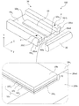
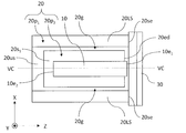
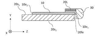
- FIG. 1A is a perspective view schematically showing a configuration example of the laser light source 100 according to the first embodiment of the present disclosure.
- FIG. 1B is a diagram schematically showing a planar configuration of the laser light source 100 of FIG. 1A.
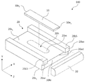
- FIG. 2A is a perspective view showing more details of the configuration in which the semiconductor laser package 40 and the pair of lead terminals 50 are omitted from the laser light source 100 of FIG. 1A.
- FIG. 2B is a top view schematically showing the laser light source 100 of FIG. 2A.
- FIG. 2C is a sectional view taken along line IIC-IIC parallel to the YZ plane having the configuration of FIG. 2B.
- FIG. 3A is a perspective view schematically showing a configuration example of the laser light source 110 according to the first modification of the first embodiment of the present disclosure.
- FIG. 3B is a top view schematically showing the laser light source 110 of FIG. 3A.
- FIG. 3C is a sectional view taken along line IIIC-IIIC parallel to the YZ plane having the configuration of FIG. 3B.
- FIG. 4A is a perspective view schematically showing a configuration example of the laser light source 120 according to the second modification of the first embodiment of the present disclosure.
- FIG. 4B is a top view schematically showing the laser light source 120 of FIG. 4A.
- FIG. 4C is a sectional view taken along line IVC-IVC parallel to the YZ plane having the configuration of FIG. 4B.
- FIG. 5A is a perspective view schematically showing a configuration example of the laser light source 130 according to the third modification of the first embodiment of the present disclosure.
- FIG. 5B is a top view schematically showing the laser light source 130 of FIG. 5A.
- FIG. 5C is a sectional view taken along line VC-VC parallel to the YZ plane having the configuration of FIG. 5B.
- FIG. 6A is a perspective view schematically showing a configuration example of the laser light source 140 in the modified example 4 of the first embodiment of the present disclosure.
- FIG. 6B is a top view schematically showing the laser light source 140 of FIG. 6A.
- FIG. 6C is a cross-sectional view taken along the line VIC-VIC parallel to the YZ plane having the configuration of FIG. 6B.
- FIG. 7A is a perspective view schematically showing a configuration example of the laser light source 150 in the modified example 5 of the first embodiment of the present disclosure.
- FIG. 7B is a top view schematically showing the laser light source 150 of FIG. 7A.
- FIG. 7C is a sectional view taken along line VIIC-VIIC parallel to the YZ plane having the configuration of FIG. 7B.
- FIG. 7D is a perspective view schematically showing a state in which the collimating lens 30 in the laser light source 150 of FIG. 7A is joined to the submount 20 by using the collet 60.
- FIG. 8A is a perspective view schematically showing a configuration example of the laser light source 200 according to the second embodiment of the present disclosure.
- FIG. 8B is a top view schematically showing the laser light source 200 of FIG.
- FIG. 8C is a sectional view taken along line VIIIC-VIIIC parallel to the YZ plane having the configuration of FIG. 8B.
- FIG. 8D is a rear view schematically showing the laser light source 200 of FIG. 8A.
- FIG. 9A is a perspective view schematically showing a configuration example of the laser light source 210 according to the first modification of the second embodiment of the present disclosure.
- 9B is a top view schematically showing the laser light source 210 of FIG. 9A.
- FIG. 9C is a sectional view taken along line IXC-IXC parallel to the YZ plane having the configuration of FIG. 9B.
- 9D is a rear view schematically showing the laser light source 210 of FIG. 9A.
- FIG. 9A is a perspective view schematically showing a configuration example of the laser light source 210 according to the first modification of the second embodiment of the present disclosure.
- 9B is a top view schematically showing the laser light source 210 of FIG. 9A.
- FIG. 9C
- FIG. 10A is a perspective view schematically showing a configuration example of the laser light source 220 in the second modification of the second embodiment of the present disclosure.
- FIG. 10B is a top view schematically showing the laser light source 220 of FIG. 10A.
- FIG. 10C is a cross-sectional view taken along the line XC-XC parallel to the YZ plane having the configuration of FIG. 10B.
- FIG. 10D is a perspective view schematically showing the fourth submount portion 20p 4 and the collimating lens 30 of FIG. 10A.
- FIG. 1A is a perspective view schematically showing a configuration example of the laser light source 100 according to the first embodiment of the present disclosure.
- FIG. 1B is a diagram schematically showing a planar configuration of the laser light source 100 of FIG. 1A.
- the laser light source 100 in the present embodiment includes a laser diode chip 10, a submount 20 that supports the laser diode chip 10, a collimating lens 30 that is supported by the submount 20, and a semiconductor laser package that houses these elements or components. 40 and.
- the laser light source 100 in the present embodiment includes a pair of lead terminals 50 that penetrate the semiconductor laser package 40 and supply electric power to the laser diode chip 10.
- the semiconductor laser package 40 includes a lid 40L, a substrate 40b, and a translucent window 40w. In the laser light source 100 of the present embodiment, the laser light emitted from the laser diode chip 10 and collimated by the collimating lens 30 is taken out from the translucent window 40w.
- FIG. 1A the lid 40L, the substrate 40b, and the translucent window 40w in the semiconductor laser package 40 are shown in a separated state for the sake of clarity of explanation, but they are actually joined.
- FIG. 1B the description of the lid 40L in the semiconductor laser package 40 is omitted.
- the X-axis, Y-axis, and Z-axis that are orthogonal to each other are schematically shown.
- the side in which the laser diode chip 10, the submount 20, and the collimating lens 30 are located in the substrate 40b may be referred to as "upper" in the present disclosure. This does not limit the orientation of the laser light source 100 when it is used, and the orientation of the laser light source 100 is arbitrary.
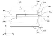
- FIG. 2A is a perspective view showing more details of the configuration in which the semiconductor laser package 40 and the pair of lead terminals 50 are omitted from the laser light source 100 of FIG. 1A.
- the region surrounded by the broken line in FIG. 2A represents an example of the detailed structure of the laser diode chip 10 arranged on the submount 20.
- the submount 20 and the collimating lens 30 are shown in a separated state, but they are actually joined.
- FIG. 2B is a top view schematically showing the laser light source 100 of FIG. 2A.
- FIG. 2C is a sectional view taken along line IIC-IIC parallel to the YZ plane having the configuration of FIG. 2B.
- the side on which the collimating lens 30 is located may be referred to as "forward" with reference to the submount 20.
- the laser diode chip 10 is an end face emission type laser diode chip, and is a semiconductor laminated structure 10a including a first clad layer 10C 1, a second clad layer 10C 2, and a light emitting layer 10L. It has a substrate 10b that supports the semiconductor laminated structure 10a, an emission end surface 10e 1 that emits high-power laser light generated by the light emitting layer 10L, and a rear end surface 10e 2 that is opposite to the emission end surface 10e 1. ..
- the light emitting layer 10L is located between the first clad layer 10C 1 and the second clad layer 10C 2.
- the laser diode chip 10 may include other layers such as a buffer layer and a contact layer.
- the "exiting end face 10e 1 " may be referred to as a "first end face 10e 1”
- the "rear end face 10e 2 " may be referred to as a " second end face 10e 2".
- the laser diode chip 10 is fixed to the submount 20 in a face-down state in which the light emitting layer 10L is closer to the submount 20 than the substrate 10b.
- the total size of the semiconductor laminated structure 10a and the substrate 10b in the laser diode chip 10 in the Y direction is about 80 ⁇ m.
- the total size of the substrate 10b and the first clad layer 10C 1 in the Y direction is larger than the size of the second clad layer 10C 2 in the Y direction.
- the distance between the light emitting layer 10L and the submount 20 is about 1/10 as compared with the face-up state in which the light emitting layer 10L is farther from the submount 20 than the substrate 10b.
- the heat generated by the light emitting layer 10L can be efficiently transferred to the submount 20.
- the output of the laser beam in this embodiment is, for example, 3 W or more and 50 W or less.
- the semiconductor laminated structure 10a may have, for example, a double heterostructure forming an energy level of a quantum well.
- the bandgap of the light emitting layer 10L is smaller than the bandgap of the first clad layer 10C 1 and the second clad layer 10C 2.
- the substrate 10b and the first clad layer 10C 1 on the substrate 10b can each be formed from an n-type semiconductor.
- the light emitting layer 10L may be formed of an intrinsic semiconductor, an n-type semiconductor, or a p-type semiconductor, and the second clad layer 10C 2 on the light emitting layer 10L may be formed of a p-type semiconductor.
- the n-type and the p-type may be reversed.
- the current injection from the p-type clad layer to the n-type clad layer causes a carrier inversion distribution in the light emitting layer 10L, and light is stimulated and emitted from the light emitting layer 10L.
- the refractive index of the light emitting layer 10L is designed to be higher than the refractive index of the first clad layer 10C 1 and the second clad layer 10C 2 , and the light generated by the light emitting layer 10L is totally reflected into the light emitting layer 10L. Be trapped.
- the light emitting layer 10L functions as a resonator, and laser light is emitted from the emission end face 10e 1 of the light emitting layer 10L.
- the cavity length of the light emitting layer 10L is defined by the distance from the exit end face 10e 1 to the rear end face 10e 2.
- the direction of the cavity length is parallel to the Z direction.
- the resonator length is, for example, 500 ⁇ m or more and 5000 ⁇ m or less. When the resonator length is long, the contact area between the laser diode chip 10 and the submount 20 can be widened, so that the heat generated in the light emitting layer 10L can be efficiently transferred to the submount 20.
- the laser beam emitted from the emission end face 10e 1 of the laser diode chip 10 diverges quickly in the YZ plane and diverges slowly in the XZ plane as it propagates.
- the spot of the laser beam is a far field and has an elliptical shape in which the Y direction is the major axis and the X direction is the minor axis in the XY plane.
- the laser diode chip 10 can emit purple, blue, green or red laser light in the visible region, or infrared or ultraviolet laser light.
- the emission peak wavelength of purple is preferably in the range of 350 nm or more and 419 nm or less, and more preferably in the range of 400 nm or more and 415 nm or less.
- the emission peak wavelength of blue light is preferably in the range of 420 nm or more and 494 nm or less, and more preferably in the range of 440 nm or more and 475 nm or less.
- Examples of the semiconductor laser device that emits a purple or blue laser beam include a semiconductor laser device containing a nitride semiconductor.
- the nitride semiconductor for example, GaN, InGaN, and AlGaN can be used.
- the emission peak wavelength of green light is preferably in the range of 495 nm or more and 570 nm or less, and more preferably in the range of 510 nm or more and 550 nm or less.
- the semiconductor laser device that emits a green laser beam include a semiconductor laser device containing a nitride semiconductor.
- the nitride semiconductor for example, GaN, InGaN, and AlGaN can be used.
- the emission peak wavelength of red light is preferably in the range of 605 nm or more and 750 nm or less, and more preferably in the range of 610 nm or more and 700 nm or less.
- the semiconductor laser device that emits a red laser beam include a semiconductor laser device including an InAlGaP-based, GaInP-based, GaAs-based, and AlGaAs-based semiconductor.
- the red light semiconductor laser device a semiconductor laser device having two or more waveguide regions can be used. A semiconductor laser device containing these semiconductors tends to have a lower output due to heat than a semiconductor laser device containing a nitride semiconductor. By increasing the waveguide region, heat can be dispersed and the output decrease of the semiconductor laser device can be reduced.
- the submount 20 is located on the opposite side of the main plane 20s 1 to which the laser diode chip 10 is fixed, the pair of lens support portions 20LS located on both sides of the emission end surface 10e 1 of the laser diode chip 10, and the main plane 20s 1. has a rear surface 20s 2 which, the front end surface 20fe connecting the main planes 20s 1 and the back 20s 2.
- the main plane 20s 1 and the front end face 20fe define the edge 20ed of the main plane 20s 1.
- the pair of lens support portions 20LS are a pair of convex portions located on both sides of the laser diode chip 10 and extending in the Z direction.
- the submount 20 has the following U-shape extending in the Z direction behind the front end surface 20fe.
- This U-shape is mirror-symmetrical with respect to a plane parallel to the YZ plane, and is formed by dividing a square cylinder extending in the Z direction by a plane parallel to the XZ plane.
- the end faces 20se of the pair of lens support portions 20LS project in the resonator length direction from the emission end faces 10e 1 of the laser diode chip 10.
- the normal direction of the main plane 20s 1 is parallel to the Y direction.
- the distance between the end face 20se of the pair of lens support portions 20LS and the emission end face 10e 1 of the laser diode chip 10 in the Z direction can be designed to be substantially equal to the focal length of the collimating lens 30.
- the distance between the end face 20se of the pair of lens support portions 20LS and the emission end face 10e 1 of the laser diode chip 10 in the Z direction is, for example, 50 ⁇ m or more and 100 ⁇ m or less.
- the size of the pair of lens support portions 20LS in the Y direction may be similar to the size of the collimating lens 30 in the Y direction.
- the size of the pair of lens support portions 20LS in the Y direction may be larger, equal to, or smaller than the size of the collimating lens 30 in the Y direction.
- the size of the pair of lens support portions 20LS in the Y direction is, for example, 100 ⁇ m or more and 500 ⁇ m or less.
- the size of the sub-mount 20 in the X direction is, for example, 1 mm or more and 3 mm or less
- the size of the portion of the sub-mount 20 other than the pair of lens support portions 20LS in the Y direction is, for example, 100 ⁇ m or more and 500 ⁇ m or less, and a pair.
- the size of the portion other than the lens support portion 20LS in the Z direction is, for example, 1 mm or more and 6 mm or less.
- the upper limit of the size can be determined from the viewpoint of miniaturization of the laser light source 100.
- the emission end surface 10e 1 of the laser diode chip 10 projects in the resonator length direction from the edge 20ed of the main plane 20s 1.
- the distance between the emission end face 10e 1 of the laser diode chip 10 and the edge 20ed of the main plane 20s 1 in the Z direction is, for example, 2 ⁇ m or more and 50 ⁇ m or less.
- the bonding material for joining the laser diode chip and the submount is attached to the emission end face of the light emitting layer in the laser diode chip.
- the output of the laser beam emitted from the laser diode chip may decrease.
- such a decrease in the output of the laser light can be suppressed.
- Part or all of the submount 20 may be formed from an alloy such as ceramic and CuW containing at least one selected from the group consisting of, for example, AlN, SiC, and alumina.
- the submount 20 can be made, for example, by sintering ceramic powder.
- the thermal conductivity of the ceramic can be, for example, 10 [W / m ⁇ K] or more and 500 [W / m ⁇ K] or less.
- the ceramic may have a low coefficient of thermal expansion in order to suppress deformation due to heat applied when the laser diode chip 10 is fixed.
- the coefficient of thermal expansion can be 2 ⁇ 10 -6 [1 / K] or more and 1 ⁇ 10 -5 [1 / K] or less.
- a metal film such as gold plating having a thickness of, for example, 0.5 ⁇ m or more and 10 ⁇ m or less may be formed on the main plane 20s 1 and the back surface 20s 2 of the submount 20.
- the metal film formed on the main plane 20s 1 allows the laser diode chip 10 to be joined to the main plane 20s 1 with , for example, gold tin.
- the metal film formed on the back surface 20s 2 allows the submount 20 to be joined to the bottom 40b 1 with , for example, gold tin.
- the collimator lens 30 is a so-called FAC (Fast Axis Collimator) lens that collimates a component of the laser light emitted from the laser diode chip 10 that is largely diverged in the YZ plane.
- a so-called SAC (Slow Axis Collimator) lens (not shown) that collimates a small divergent component of the laser beam in the XZ plane can be arranged outside the laser light source 100, if necessary.
- "collimating” includes not only making the laser light parallel light but also reducing the divergence angle of the laser light.
- another lens such as a condenser lens may be used instead of the collimating lens 30.
- the collimating lens 30 is a cylindrical lens having a structure extending in the X direction, and has no curvature in the X-axis direction and has a curvature in the Y direction.
- the direction in which the collimating lens 30 extends is a direction perpendicular to both the normal direction of the main plane 20s 1 of the submount 20 and the longitudinal direction of the resonator. Since the size of the collimating lens 30 and the pair of lens support portions 20LS in the Y direction are about the same, the center of gravity of the collimating lens 30 is located between the pair of lens support portions 20LS when viewed from the resonator length direction. It is easy to install in. Due to this arrangement of the center of gravity of the collimating lens 30, the collimating lens 30 can be stably and accurately provided on the submount 20.
- the height of the upper surface of the pair of lens support portions 20LS in the Y direction is substantially equal to the height of the upper surface of the collimating lens 30 in the Y direction when the back surface 20s 2 of the submount 20 is used as a reference.
- the position of the collimating lens 30 with respect to the pair of lens support portions 20LS is roughly adjusted so that the above two heights are substantially equal to each other.
- the position of the collimating lens 30 with respect to the pair of lens support portions 20LS is finely adjusted so that the laser beam is appropriately collimated.
- the above two heights do not necessarily have to be substantially equal, and may be different.
- the collimating lens 30 in the present embodiment is uniform along the X direction, it is not necessary to consider the alignment of the emission end surface 10e 1 of the laser diode chip 10 with the collimating lens 30 in the X direction.
- the collimating lens 30 only the facing portion and the peripheral portion thereof opposite to the emitting end face 10e 1 of the laser diode chip 10 may be a uniform along the X direction. Therefore, the other side portions do not necessarily have to be uniform along the X direction and need not be transparent.
- the size of both side portions of the collimating lens 30 in the Y direction may be larger, equal to, or smaller than the size of the opposing portion and its peripheral portion in the Y direction.
- the collimating lens 30 can be formed from, for example, at least one of glass, quartz, synthetic quartz, sapphire, clear ceramic, and plastic.
- the collimating lens 30 is joined to the end faces 20se of the pair of lens support portions 20LS in the Z direction. Even if there is some variation in the thickness of the bonding material that joins the collimating lens 30 and the end face 20se of the pair of lens support portions 20LS, the variation has almost no effect on the position of the collimating lens 30 in the Y direction. Unlike the configuration of the present embodiment, it is also possible to arrange a pedestal having a plane parallel to the main plane 20s 1 in front of the submount 20 and provide the collimating lens 30 on the plane of the pedestal.
- the position of the laser diode chip 10 and the collimating lens 30 shifts in the Y direction, and the laser light source There is a possibility that the direction of the optical axis of the laser beam emitted from the 100 to the outside is greatly deviated.
- the positional deviation between the laser diode chip 10 and the collimating lens 30 in the Y direction is less likely to occur, and the optical axis of the laser light emitted to the outside from the laser light source 100 is directed in the design direction. be able to.
- the position of the collimating lens 30 Even if there is some variation in the thickness of the bonding material, the position of the collimating lens 30 only changes slightly along the optical axis of the laser beam, so that variation has almost no effect on the direction of the optical axis of the laser beam. Absent.
- the collimating lens 30 and the end face 20se of the pair of lens support portions 20LS can be joined with a bonding material of an inorganic material such as gold tin.
- a metal film may be formed in advance on the joint surface of the collimating lens 30 and the end surface 20se of the pair of lens support portions 20LS. These metal films allow for joining with, for example, gold tin.
- the bonding temperature of gold tin is about 280 ° C. If the thermal conductivity of the ceramic forming the submount 20 is low, it is possible to reduce the influence of the heat at the time of joining the collimating lens 30 and the end faces 20se of the pair of lens support portions 20LS on the laser diode chip 10.
- the collimating lens 30 and the end face 20se of the pair of lens support portions 20LS can be joined by a bonding material containing a thermosetting resin.
- the bonding temperature of the thermosetting resin is about 100 ° C., which is lower than the bonding temperature of the inorganic material. Therefore, it is possible to further reduce the influence of the heat at the time of joining the collimating lens 30 and the end faces 20se of the pair of lens support portions 20LS on the laser diode chip 10.
- the thermosetting resin can be heated, for example, by irradiating the position of the point P shown in FIG. 2A with a laser beam.
- the distance between the position of the point P and the end face 20se of the pair of lens support portions 20LS in the Z direction is, for example, 50 ⁇ m or more and 500 ⁇ m or less.
- the outgas is a laser. It is possible to suppress the approach to the diode chip 10. As a result, it is possible to suppress the occurrence of dust collection described later on the emission end face 10e 1 of the laser diode chip 10.
- Some inorganic materials may contain organic substances as binders. Even if the bonding material is used for bonding the collimating lens 30 and the end surface 20se of the pair of lens support portions 20LS, it is possible to prevent the outgas generated by heating from approaching the laser diode chip 10.
- the collimating lens 30 and the end face 20se of the pair of lens support portions 20LS may be joined by direct bonding without using a joining material.
- direct bonding include diffusion bonding, room temperature bonding, and anodic bonding.
- the misalignment of the collimating lens 30 in the Y direction can be suppressed as in the bonding using the bonding material.
- the submount 20 supports the laser diode chip 10 and the collimating lens 30. Since the distance between the emission end face 10e 1 of the laser diode chip 10 and the collimating lens 30 is short, it is possible to reduce the divergence of the laser light emitted from the laser diode chip 10 by the small collimating lens 30 before it is largely diverged. it can. Therefore, it is possible to realize a small laser light source 100. Further, the diameter of the collimating beam that has passed through the collimating lens 30 can be reduced.
- the semiconductor laser package 40 may airtightly seal the laser diode chip 10, the submount 20, and the collimating lens 30.
- the laser diode chip 10 emits a laser beam having a short wavelength of, for example, 350 nm or more and 570 nm or less
- the organic gas component contained in the atmosphere is decomposed by the laser beam, and the decomposed product is transferred to the emission end surface 10e 1 of the laser diode chip 10. May adhere.
- the emission end face 10e 1 of the laser diode chip 10 is in contact with the outside air, the end face deterioration may progress during the operation due to dust collection or the like. Such end face deterioration can lead to a decrease in the optical output of the laser diode chip 10.
- the semiconductor laser package 40 tightly seals the laser diode chip 10.
- the airtight sealing by the semiconductor laser package 40 may be performed regardless of the length of the wavelength of the laser light emitted from the laser diode chip 10.
- the substrate 40b in the semiconductor laser package 40 is in thermal contact with the back surface 20s 2 of the submount 20.
- the substrate 40b can be formed from a material having high thermal conductivity.
- the material is, for example, a metal containing at least one selected from the group consisting of Cu, Al, Ag, Fe, Ni, Mo, Cu, W, and CuMo.
- the thermal conductivity is high between the bottom surface 40bt of the substrate 40b and the submount 20 in order to match the heights of the emission end surface 10e 1 of the laser diode chip 10 and the translucent window 40w.
- a member 40 m may be provided.
- the member 40m can be made of the same material as the portion of the substrate 40b that includes the bottom surface 40bt.
- the submount 20 may be arranged on the raised bottom surface 40bt.
- the portion of the substrate 40b that includes the bottom surface 40 bt can be formed, for example, from copper.
- the portion of the substrate 40b that surrounds the laser diode 10, the submount 20, and the collimating lens 30 can be formed, for example, from Kovar.
- Kovar is an alloy in which nickel and cobalt are added to iron, which is the main component.
- the lid 40L in the semiconductor laser package 40 may be formed of the same material as the substrate 40b, or may be formed of a different material.
- the translucent window 40w in the semiconductor laser package 40 is attached to the substrate 40b and transmits the laser light emitted from the laser diode chip 10.
- the translucent window 40w in the semiconductor laser package 40 can be formed from, for example, at least one of glass, quartz, synthetic quartz, sapphire, transparent ceramic, and plastic, similar to the collimating lens 30.
- Each of the pair of lead terminals 50 is electrically connected to the laser diode chip 10 by a wire as follows.
- a metal film such as gold plating is formed on the upper surface of the laser diode chip 10.
- the metal film and one of the pair of lead terminals 50 are electrically connected by a wire.
- a metal film such as gold plating is formed on the main plane 20s 1 of the submount 20.
- the metal film and the other of the pair of lead terminals 50 are electrically connected by a wire.
- a current is injected from the second clad layer 10C 2 to the first clad layer 10C 1 in the laser diode chip 10 by the pair of lead terminals 50.
- the pair of lead terminals 50 are electrically connected to an external circuit (not shown) that adjusts the emission timing and output of the laser beam emitted from the laser diode chip 10.
- the pair of lead terminals 50 are made of a material having good conductivity. Examples of the material include metals such as Fe—Ni alloys and Cu alloys.
- the submount 20 supports the laser diode chip 10 by the main plane 20s 1 between the pair of lens support portions 20LS, and the collimating lens 30 is supported by the end faces 20se of the pair of lens support portions 20LS. I support it.
- the alignment between the laser diode chip 10 and the collimating lens 30 becomes easy, and a compact laser light source 100 can be realized.
- it laser diode chip 10 is also disposed face down on a submount 20, to prevent the bonding material rises parsley the outgoing end face 10e 1 of the laser diode chip 10 Can be done.
- FIG. 3A is a perspective view schematically showing a configuration example of the laser light source 110 according to the first modification of the first embodiment of the present disclosure.
- FIG. 3B is a top view schematically showing the laser light source 110 of FIG. 3A.
- FIG. 3C is a sectional view taken along line IIIC-IIIC parallel to the YZ plane having the configuration of FIG. 3B.
- the difference between the laser light source 110 in the first modification of the first embodiment and the laser light source 100 in the first embodiment is the shape of the submount 20.
- the front end face 20fe in the submount 20 has a central end face 20fe 1 and both side end faces 20fe 2 located on both sides of the central end face 20fe 1 .
- the central end face 20fe 1 is recessed in the resonator length direction with respect to both side end faces 20fe 2.
- Edge 20ed main plane 20s 1 in Modification 1 of Embodiment 1 is defined by a main plane 20s 1 and the central end surface 20Fe 1.
- the size of the depression of the central end surface 20fe 1 in the Z direction is, for example, 5 ⁇ m or more and 100 ⁇ m or less
- the size in the X direction is, for example, 50 ⁇ m or more and 200 ⁇ m or less
- the size from the main plane 20s 1 in the Y direction is, for example, 100 ⁇ m or more. It is 500 ⁇ m or less.
- the recess does not necessarily have to penetrate in the Y direction.
- the emission end surface 10e 1 of the laser diode chip 10 projects in the resonator length direction from the edge 20ed of the main plane 20s 1 defined by the main plane 20s 1 and the central end surface 20fe 1.
- the both end faces 20fe 2 of the submount 20 project in the resonator length direction from the emission end faces 10e 1 of the laser diode chip 10, similarly to the end faces 20se of the pair of lens support portions 20LS.
- the edge 20ed of the main plane 20s 1 defined by the main plane 20s 1 and the central end face 20fe 1 can prevent the bonding material from rising to the exit end face 10e 1 of the laser diode chip 10.
- the sub-mount 20 according to the first modification of the first embodiment may be easily manufactured because only a part of the front end surface 20fe needs to be removed in the above-mentioned U-shape extending in the Z direction. Further, since the collimating lens 30 is joined to the L-shaped end face including the end face 20se and both side end faces 20fe 2 of the pair of lens support portions 20LS, the contact area between the collimating lens 30 and the submount 20 is widened, and the collimating lens 30 is joined. Can be easy.
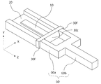
- FIG. 4A is a perspective view schematically showing a configuration example of the laser light source 120 according to the second modification of the first embodiment of the present disclosure.
- FIG. 4B is a top view schematically showing the laser light source 120 of FIG. 4A.
- FIG. 4C is a sectional view taken along line IVC-IVC parallel to the YZ plane having the configuration of FIG. 4B.
- the difference between the laser light source 120 in the second modification of the first embodiment and the laser light source 100 in the first embodiment is the shape of the submount 20.
- the submount 20 in the second modification of the first embodiment has a groove 20d extending along the length direction of the resonator between each of the pair of lens support portions 20LS and the laser diode chip 10.
- the groove 20d is adjacent to the pair of lens support portions 20LS, but it is not always necessary to be adjacent to the groove 20d.
- the size in the X direction of the grooves 20d and for example 100 ⁇ m or 500 ⁇ m or less, the size in the Y direction is, for example, 50 ⁇ m or 300 ⁇ m or less, the size of the main plane 20s 1 edge 20ed in the Z direction, for example, 1mm or 6mm It is as follows.
- the groove 20d does not necessarily have to penetrate in the Z direction.
- the groove 20d can reduce the influence of heat on the laser diode chip 10 at the time of joining the collimating lens 30 and the end face 20se of the pair of lens support portions 20LS.
- FIG. 5A is a perspective view schematically showing a configuration example of the laser light source 130 according to the third modification of the first embodiment of the present disclosure.
- FIG. 5B is a top view schematically showing the laser light source 130 of FIG. 5A.
- FIG. 5C is a sectional view taken along line VC-VC parallel to the YZ plane having the configuration of FIG. 5B.
- the difference between the laser light source 130 in the third modification of the first embodiment and the laser light source 100 in the first embodiment is the configuration of the submount 20.
- the submount 20 in the third modification of the first embodiment includes a first submount portion 20p 1 and a second submount portion 20p 2 .
- the first submount portion 20p 1 has a pair of lens support portions 20LS on the upper surface 20us.
- the first submount portion 20p 1 has the above-mentioned U-shape extending in the Z direction.
- the first submount portion 20p 1 may be formed from an alloy such as ceramic and CuW containing at least one selected from the group consisting of, for example, AlN, SiC, and alumina.
- the second submount portion 20p 2 is fixed to the upper surface 20us of the first submount portion 20p 1 and is located between the pair of lens support portions 20LS.
- the second submount portion 20p 2 has a main plane 20s 1 on which the laser diode chip 10 is mounted and a front end surface 20fe facing the collimating lens 30.
- the main plane 20s 1 is a surface of the first submount portion 20p 1 on the side opposite to the surface fixed to the upper surface 20us. In the present disclosure, it is not necessary that the front end surface 20fe and the back surface 20s 2 are directly connected. In this disclosure, to one side of the front end surface 20Fe, and in contact with one side of the main plane 20s 1, one side and the main plane 20s 1 front end surface 20Fe contact defines a main plane 20s 1 edge 20Ed.
- the second submount portion 20p 2 may be formed from at least one selected from the group consisting of, for example, Cu, Al, Ag, Fe, Ni, Mo, Cu, W, CuW, CuMo, AlN, SiC and alumina. ..
- the size of the second submount portion 20p 2 in the X direction is, for example, 0.5 mm or more and 1.5 mm or less
- the size in the Y direction is, for example, 0.1 mm or more and 0.5 mm or less
- the size in the Z direction is. For example, it is 1 mm or more and 6 mm or less.
- the first sub-mount portions 20p 1 and the second sub-mount portions 20p 2 are separate, the second position of the sub-mount portion 20p 2 on the first sub-mount portions 20p 1 Can be adjusted.
- the portion having the main plane 20s 1 and the portion having the pair of lens support portions 20LS may be separate bodies.
- the size of the void 20 g in the X direction is, for example, 50 ⁇ m or more and 300 ⁇ m or less.
- the size of the gap 20g in the Y and Z directions is determined by the size of the second submount portion 20p 2 in the Y and Z directions, respectively.
- the gap 20 g reduces the influence of heat on the laser diode chip 10 at the time of joining the collimating lens 30 and the end face 20se of the pair of lens support portions 20LS, similarly to the laser light source 120 in the second modification of the first embodiment. Can be done.
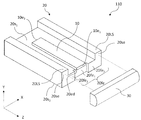
- FIG. 6A is a perspective view schematically showing a configuration example of the laser light source 140 in the modified example 4 of the first embodiment of the present disclosure.
- the laser diode chip 10, the submount 20, and the collimating lens 30 are shown in a separated state, but they are actually joined.
- FIG. 6B is a top view schematically showing the laser light source 140 of FIG. 6A.
- FIG. 6C is a cross-sectional view taken along the line VIC-VIC parallel to the YZ plane having the configuration of FIG. 6B.
- the difference between the laser light source 140 in the fourth modification of the first embodiment and the laser light source 100 in the first embodiment is the configuration of the submount 20.
- the submount 20 in the fourth modification of the first embodiment has a through hole 20h reaching from the main plane 20s 1 to the back surface 20s 2 and a metal 20m filling the through hole 20h.
- the portion of the submount 20 other than the through hole 20h can be formed of, for example, ceramic.
- the metal 20m has a high thermal conductivity and may include, for example, at least one selected from the group consisting of Cu, Al, Ag, Fe, Ni, Mo, Cu, W, and CuMo.
- the maximum size of the metal 20 m in the X direction is, for example, 0.5 mm or more and 1.5 mm or less, and the maximum size in the Z direction is, for example, 1 mm or more and 6 mm or less.
- the metal 20 m may be entirely overlapped with the laser diode chip 10 or may be partially overlapped with the laser diode chip 10 in a top view. By arranging the laser diode chip 10 in contact with the metal 20 m in the submount 20, the heat generated from the laser diode chip 10 can be efficiently transferred to the semiconductor laser package 40 via the metal 20 m.
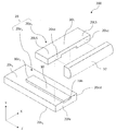
- FIG. 7A is a perspective view schematically showing a configuration example of the laser light source 150 in the modified example 5 of the first embodiment of the present disclosure.
- FIG. 7B is a top view schematically showing the laser light source 150 of FIG. 7A.
- FIG. 7C is a sectional view taken along line VIIC-VIIC parallel to the YZ plane having the configuration of FIG. 7B.
- the difference between the laser light source 150 in the modified example 5 of the first embodiment and the laser light source 100 in the first embodiment is the shape of the collimating lens 30.
- the collimating lens 30 in the fifth modification of the first embodiment has a pair of flat portions 30f and a lens curved portion 30c sandwiched between the pair of flat portions 30f.
- the lens curved surface portion 30c in the modified example 5 of the first embodiment functions as an FAC lens in the same manner as the collimating lens 30 in the first embodiment.
- FIG. 7D is a perspective view schematically showing a state in which the collimating lens 30 in the laser light source 150 of FIG. 7A is joined to the submount 20 by using the collet 60.
- the collet 60 has a bifurcated portion 60a and a support portion 60b connected to the bifurcated portion 60a.
- the collet 60 has a hollow structure and can attract and support the collimating lens 30. Specifically, the tip of the bifurcated portion 60a of the collet 60 attracts the pair of flat portions 30f of the collimating lens 30.
- the support portion 60b is held by the mounting device, the collimating lens 30 is supported by the bifurcated portion 60a, and the collimating lens 30 is joined to the submount 20 so as to be perpendicular to the end surface 20se of the pair of lens support portions 20LS.
- the load can be applied stably in various directions. With the load applied, the bonding material between the collimating lens 30 and the end face 20se of the pair of lens support portions 20LS is heated.
- a mirror may be provided between the bifurcated portions 60a of the collet 60.
- the collimating lens 30 is joined to the submount 20 while emitting the laser beam from the laser diode chip 10 in the Z direction, and the laser beam reflected in the Y direction by a mirror (not shown) is received by the light receiving device to form the collimating lens 30.
- the alignment of the laser diode chip 10 with the emission end face 10e 1 can be performed with high accuracy.
- the light receiving device can be, for example, a power meter, a parallelism measuring instrument, or a beam profiler.
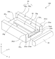
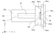
- FIG. 8A is a perspective view schematically showing a configuration example of the laser light source 200 according to the second embodiment of the present disclosure.
- FIG. 8B is a top view schematically showing the laser light source 200 of FIG. 8A.
- FIG. 8C is a sectional view taken along line VIIIC-VIIIC parallel to the YZ plane having the configuration of FIG. 8B.
- FIG. 8D is a rear view schematically showing the laser light source 200 of FIG. 8A.
- the difference between the laser light source 200 in the second embodiment and the laser light source 100 in the first embodiment is the configuration of the submount 20.
- the submount 20 in the second embodiment includes a third submount portion 20p 3 and a fourth submount portion 20p 4 .
- the third submount portion 20p 3 has a main plane 20s 1 , a back surface 20s 2 , and a front end surface 20fe.
- the fourth submount portion 20p 4 has a pair of lens support portions 20LS fixed to the main plane 20s 1 of the third submount portion 20p 3 and a connecting portion 20L connecting the pair of lens support portions 20LS. Connecting portion 20L connects the pair of lens support portions 20LS so as not to interfere with the propagation of laser light emitted from the emission end surface 10e 1 of the laser diode chip 10.
- the third submount portion 20p 3 and the fourth submount portion 20p 4 are separate bodies.
- the portion having the main plane 20s 1 and the portion having the pair of lens support portions 20LS may be separate bodies.
- the third submount portion 20p 3 , the fourth submount portion 20p 4 , and the collimating lens 30 are described in a separated state, but they are actually joined.
- the pair of lens support portions 20LS and the connecting portion 20L in the fourth submount portion 20p 4 are integrally molded.
- the connecting portion 20L overlaps the emission end surface 10e 1 of the laser diode chip 10 in top view.
- the fourth submount portion 20p 4 is arranged on the main plane 20s 1 of the third submount portion 20p 3 so as to straddle the laser diode chip 10. Since the size of the fourth submount portion 20p 4 in the X direction is larger than the size of the third submount portion 20p 3 in the X direction, the area of the end faces 20se of the pair of lens support portions 20LS can be increased. .. As a result, it becomes easy to join the collimating lens 30 to the end faces 20se of the pair of lens support portions 20LS.
- the size of the pair of lens support portions 20LS of the fourth submount portion 20p 4 in the Y direction may be similar to the size of the collimating lens 30 in the Y direction.
- the size of the pair of lens support portions 20LS of the fourth submount portion 20p 4 in the Y direction may be larger, equal to, or smaller than the size of the collimating lens 30 in the Y direction.
- the size of the fourth submount portion 20p 4 in the X direction is, for example, 0.5 mm or more and 4 mm or less
- the maximum size in the Y direction is, for example, 0.5 mm or more and 2 mm or less
- the size in the Z direction is, for example, It is 0.5 mm or more and 1 mm or less.
- the third submount part and step of the main plane 20s 1 bonding the laser diode chip 10 of the 20p 3, third sub-mount portion so as to straddle the laser diode chip 10 20p
- the third sub-mount portions 20p 3 of the laser diode chip 10 is joined to the main plane 20s 1, may be joined to the fourth sub-mount portions 20p 4 to the collimator lens 30 are joined.
- the submount 20 a laser diode chip 10 is supported by the main plane 20s 1 between the pair of lens support portions 20LS, a pair of lenses
- the collimating lens 30 is supported by the end surface 20se of the support portion 20LS. This facilitates the alignment of the laser diode chip 10 and the collimating lens 30, and makes it possible to realize a compact laser light source 200.
- the bonding material emits the laser diode chip 10. it is possible to suppress the rise parsley on the end surface 10e 1.
- FIG. 9A is a perspective view schematically showing a configuration example of the laser light source 210 according to the first modification of the second embodiment of the present disclosure.
- 9B is a top view schematically showing the laser light source 210 of FIG. 9A.
- FIG. 9C is a sectional view taken along line IXC-IXC parallel to the YZ plane having the configuration of FIG. 9B.
- 9D is a rear view schematically showing the laser light source 210 of FIG. 9A.
- the difference between the laser light source 210 in the first modification of the second embodiment and the laser light source 200 in the second embodiment is the shape of the fourth submount portion 20p4 in the submount 20.
- the fourth submount portion 20p 4 in the first modification of the second embodiment has a notch 20co between the pair of lens support portions 20LS in the fourth submount portion 20p 4 in the second embodiment. Due to the notch 20co, as shown in FIGS. 9B and 9C, the connecting portion 20L does not overlap the emitting end surface 10e 1 of the laser diode chip 10 in top view.
- the size of the notch 20co in the X direction is, for example, 0.2 mm or more and 3 mm or less, and the size in the Z direction is, for example, 0.5 mm or more and 1 mm or less.
- Notch size in the Z direction 20co has an end surface 20se of the pair of lens support portions 20LS, larger than the size in the Z direction between the third sub-mount portion 20p of 3 in the main plane 20s 1 edge 20Ed.
- FIG. 10A is a perspective view schematically showing a configuration example of the laser light source 220 in the second modification of the second embodiment of the present disclosure.
- FIG. 10B is a top view schematically showing the laser light source 220 of FIG. 10A.
- FIG. 10C is a cross-sectional view taken along the line XC-XC parallel to the YZ plane having the configuration of FIG. 10B.
- FIG. 10D is a perspective view schematically showing the fourth submount portion 20p 4 and the collimating lens 30 shown in FIG. 10A.
- the difference between the laser light source 220 in the second modification of the second embodiment and the laser light source 200 in the second embodiment is the fourth submount portion 20p 4 in the submount 20 and the collimating lens 30.
- the fourth submount portion 20p 4 and the collimating lens 30 in the second modification of the second embodiment are integrally molded. Since it is not necessary to join the fourth submount portion 20p 4 and the collimating lens 30, the size of the fourth submount portion 20p 4 in the X direction in the second modification of the second embodiment is the fourth size in the second embodiment. It does not have to be as large as the size of the submount portion 20p 4 in the X direction.
- the size of the fourth submount portion 20p 4 in the second modification of the second embodiment in the X direction is, for example, 0.2 mm or more and 3 mm or less, and the maximum size in the Y direction is, for example, 0.3 mm or more and 1 mm or less.
- the size in the Z direction is, for example, 0.5 mm or more and 1 mm or less.
- the integrally molded fourth submount portion 20p 4 and the collimating lens 30 can be formed from, for example, at least one of glass, quartz, synthetic quartz, sapphire, transparent ceramic, and plastic.
- the integrally molded fourth submount portion 20p 4 and the collimating lens 30 are transparent, the alignment between the emission end face 10e 1 of the laser diode chip 10 and the collimating lens 30 becomes easy.
- the laser light source of the present disclosure can be used, for example, as a light source of a direct diode laser that combines a plurality of laser beams to increase the output. Beam coupling is performed by accurately coupling the laser beams emitted from a plurality of laser light sources. A high-intensity laser beam having a wavelength of 570 nm or less facilitates processing of metals such as copper.
- the position of the laser diode chip and the lens is unlikely to shift, so that the direction of the optical axis of the laser beam emitted from the laser light source to the outside does not shift significantly. It is possible to accurately combine the laser beams emitted from a plurality of laser light sources and improve the beam quality.
- the laser light source of the present disclosure can also be used, for example, in a projector and a lighting fixture.
- Laser diode chip 10a Semiconductor laminated structure 10b Substrate 10C 1 First clad layer 10C 2 Second clad layer 10e 1 Emission end face 10e 2 Rear end face 10L Light source 20 Submount 20co Notch 20d Groove 20ed Edge 20fe Front end face 20fe 1 Central end face 20fe 2 Both side end faces 20L Connecting part 20LS Lens support part 20p 1 First submount part 20p 2 Second submount part 20p 3 Third submount part 20p 4 Fourth submount part 20s 1 Main plane 20s 2 Back side 20se End face of pair of lens support parts 20us Top surface of first submount part 30 Collimated lens 30c Lens curved part 30f Flat part 40 Semiconductor laser package 40b Base 40L Lid 40w Translucent window 50 Lead terminal 60 Collet 60a 2 Also part 60b Support part 100, 110, 120, 130, 140, 150 Laser light source 200, 210, 220 Laser light source
Landscapes
- Physics & Mathematics (AREA)
- Condensed Matter Physics & Semiconductors (AREA)
- General Physics & Mathematics (AREA)
- Electromagnetism (AREA)
- Optics & Photonics (AREA)
- Semiconductor Lasers (AREA)
- Optical Head (AREA)
Abstract
Description
まず、図1Aおよび図1B、ならびに図2Aから図2Cを参照して、本開示の実施形態1におけるレーザ光源の基本的な構成例を説明する。
次に、本開示の実施形態1におけるレーザ光源100の変形例1から変形例5を説明する。以下の変形例では、半導体レーザパッケージ40、および一対のリード端子50の記載が省略されている。前述と重複する説明は省略することがある。
次に、図8Aから図8Dを参照して、本開示の実施形態2におけるレーザ光源の基本的な構成例を説明する。
次に、本開示の実施形態2におけるレーザ光源200の変形例1および変形例2を説明する。前述と重複する説明は省略することがある。
本開示のレーザ光源は、例えば、複数のレーザビームを結合して出力を高めるダイレクトダイオードレーザの光源として用いられ得る。ビーム結合は、複数のレーザ光源から出射されたレーザビームを正確に結合することによって行われる。波長が570nm以下の高強度のレーザビームによれば、例えば銅などの金属をも加工することが容易になる。本開示のレーザ光源では、レーザダイオードチップとレンズとの位置ずれが生じにくいので、レーザ光源から外部に出射されるレーザ光の光軸の向きが大きくずれることはない。複数のレーザ光源から出射されたレーザビームを正確に結合させ、ビーム品質を高めることが可能になる。
10a 半導体積層構造体
10b 基板
10C1 第1のクラッド層
10C2 第2のクラッド層
10e1 出射端面
10e2 後方端面
10L 発光層
20 サブマウント
20co 切り欠き
20d 溝
20ed エッジ
20fe 前方端面
20fe1 中央端面
20fe2 両側端面
20L 連結部
20LS レンズ支持部
20p1 第1のサブマウント部分
20p2 第2のサブマウント部分
20p3 第3のサブマウント部分
20p4 第4のサブマウント部分
20s1 主平面
20s2 裏面
20se 一対のレンズ支持部の端面
20us 第1のサブマウント部分の上面
30 コリメートレンズ
30c レンズ曲面部
30f 平坦部
40 半導体レーザパッケージ
40b 基体
40L 蓋体
40w 透光窓
50 リード端子
60 コレット
60a 二又部分
60b 支持部分
100、110、120、130、140、150 レーザ光源
200、210、220 レーザ光源
Claims (20)
- 発光層を含む半導体積層構造体と、前記半導体積層構造体を支持する基板と、前記発光層で発生したレーザ光を出射する第1の端面と、前記第1の端面とは反対側の第2の端面と、を有し、前記第1の端面から前記第2の端面までの距離によって共振器長が規定される、端面出射型のレーザダイオードチップと、
前記レーザダイオードチップが固着された主平面と、前記レーザダイオードチップの前記第1の端面の両側に位置する一対のレンズ支持部と、前記主平面の反対側に位置する裏面と、を持つサブマウントと、
前記一対のレンズ支持部の端面と接合されたレンズと、
前記レーザダイオードチップ、前記レンズ、および前記サブマウントを収容する半導体レーザパッケージと、
を備え、
前記発光層が、前記レーザダイオードチップの前記基板と比較して、前記サブマウントに近い状態で、前記レーザダイオードチップが前記サブマウントに固着されており、
前記レーザダイオードチップの前記第1の端面は、前記主平面のエッジよりも前記共振器長の方向に突出し、
前記一対のレンズ支持部の前記端面は、前記レーザダイオードチップの前記第1の端面よりも前記共振器長の方向に突出する、レーザ光源。 - 前記半導体レーザパッケージは、前記サブマウントの前記裏面に熱的に接触する基体を有し、前記レーザダイオードチップ、前記サブマウント、および前記レンズを気密に封止している、請求項1に記載のレーザ光源。
- 前記サブマウントは、前記主平面および前記裏面をつなぐ前方端面を有し、
前記前方端面は、中央端面、および前記中央端面の両側に位置する両側端面を有し、
前記中央端面は、前記両側端面よりも前記共振器長の方向に窪み、
前記主平面の前記エッジは、前記サブマウントにおける前記主平面と前記中央端面とによって規定される、請求項1または2に記載のレーザ光源。 - 前記サブマウントは、
前記一対のレンズ支持部を上面に有する第1のサブマウント部分と、
前記第1のサブマウント部分の前記上面に固定され、前記主平面を有する第2のサブマウント部分と、
を含む、請求項1または2に記載のレーザ光源。 - 前記一対のレンズ支持部のそれぞれと前記第2のサブマウント部分との間には、空隙が存在する、請求項4に記載のレーザ光源。
- 前記サブマウントは、前記一対のレンズ支持部のそれぞれと前記レーザダイオードチップとの間に、前記共振器長の方向に沿って延びる溝を有している、請求項1または2に記載のレーザ光源。
- 前記レンズは、無機材料によって、前記一対のレンズ支持部の前記端面に接合されている、請求項1から6のいずれか一項に記載のレーザ光源。
- 前記サブマウントの一部または全体は、セラミックから形成されている、請求項1から7のいずれか一項に記載のレーザ光源。
- 前記サブマウントは、前記主平面から前記裏面に達する貫通孔と、前記貫通孔を埋める金属とを有している、請求項8に記載のレーザ光源。
- 前記共振器長の方向から見たとき、前記レンズの重心は前記一対のレンズ支持部の間に位置する、請求項1から9のいずれか一項に記載のレーザ光源。
- 前記レーザ光の波長は、350nm以上570nm以下である、請求項1から10のいずれか一項に記載のレーザ光源。
- 前記レンズは、前記主平面の法線方向および前記共振器長の方向の両方に垂直な方向に沿って延びる構造を有し、
前記レンズは、前記主平面の法線方向および前記共振器長の方向の両方を含む平面内における前記レーザ光の発散角を低減する、請求項1から11のいずれか一項に記載のレーザ光源。 - 前記レンズは、一対の平坦部、および前記一対の平坦部によって挟まれたレンズ曲面部を有する、請求項1から12のいずれか一項に記載のレーザ光源。
- 前記一対のレンズ支持部は、前記レーザダイオードチップの両側において前記共振器長の方向に延びている、請求項1から13のいずれか一項に記載のレーザ光源。
- 前記サブマウントは、前記レーザダイオードチップの前記第1の端面から出射される前記レーザ光の伝搬を妨げないように前記一対のレンズ支持部を連結する連結部をさらに有する、請求項1から13のいずれか一項に記載のレーザ光源。
- 前記連結部は、上面視で、前記レーザダイオードチップの前記第1の端面と重なる、請求項15に記載のレーザ光源。
- 前記一対のレンズ支持部、および前記連結部は一体成型されている、請求項15または16に記載のレーザ光源。
- 前記一対のレンズ支持部、前記連結部、および前記レンズは一体成型されている、請求項15または16に記載のレーザ光源。
- 前記サブマウントは、前記主平面を備える第3のサブマウント部分と、前記一対のレンズ支持部を備える第4のサブマウント部分とを有し、
前記第3のサブマウント部分と前記第4のサブマウント部分とは別体である、請求項1または2に記載のレーザ光源。 - 前記レンズと前記一対のレンズ支持部の端面とは、接合材を介して接合されている、請求項1から19のいずれか一項に記載のレーザ光源。
Priority Applications (8)
| Application Number | Priority Date | Filing Date | Title |
|---|---|---|---|
| EP20906644.8A EP4084239A4 (en) | 2019-12-26 | 2020-09-08 | Laser light source |
| JP2021566816A JP7534654B2 (ja) | 2019-12-26 | 2020-09-08 | レーザ光源 |
| CN202411827449.5A CN119812928A (zh) | 2019-12-26 | 2020-09-08 | 激光光源 |
| US17/788,808 US12413040B2 (en) | 2019-12-26 | 2020-09-08 | Laser light source |
| CN202080089075.5A CN114938693B (zh) | 2019-12-26 | 2020-09-08 | 激光光源 |
| JP2024114842A JP7678389B2 (ja) | 2019-12-26 | 2024-07-18 | レーザ光源 |
| JP2025065735A JP2025106518A (ja) | 2019-12-26 | 2025-04-11 | レーザ光源 |
| US19/298,488 US20250372942A1 (en) | 2019-12-26 | 2025-08-13 | Laser light source |
Applications Claiming Priority (4)
| Application Number | Priority Date | Filing Date | Title |
|---|---|---|---|
| JP2019236440 | 2019-12-26 | ||
| JP2019-236440 | 2019-12-26 | ||
| JP2020114674 | 2020-07-02 | ||
| JP2020-114674 | 2020-07-02 |
Related Child Applications (2)
| Application Number | Title | Priority Date | Filing Date |
|---|---|---|---|
| US17/788,808 A-371-Of-International US12413040B2 (en) | 2019-12-26 | 2020-09-08 | Laser light source |
| US19/298,488 Continuation US20250372942A1 (en) | 2019-12-26 | 2025-08-13 | Laser light source |
Publications (1)
| Publication Number | Publication Date |
|---|---|
| WO2021131171A1 true WO2021131171A1 (ja) | 2021-07-01 |
Family
ID=76575868
Family Applications (1)
| Application Number | Title | Priority Date | Filing Date |
|---|---|---|---|
| PCT/JP2020/033897 Ceased WO2021131171A1 (ja) | 2019-12-26 | 2020-09-08 | レーザ光源 |
Country Status (5)
| Country | Link |
|---|---|
| US (2) | US12413040B2 (ja) |
| EP (1) | EP4084239A4 (ja) |
| JP (3) | JP7534654B2 (ja) |
| CN (2) | CN114938693B (ja) |
| WO (1) | WO2021131171A1 (ja) |
Cited By (2)
| Publication number | Priority date | Publication date | Assignee | Title |
|---|---|---|---|---|
| US20220416501A1 (en) * | 2021-06-25 | 2022-12-29 | Nichia Corporation | Laser light source |
| JP2023116097A (ja) * | 2022-02-09 | 2023-08-22 | 浜松ホトニクス株式会社 | レーザモジュール |
Families Citing this family (2)
| Publication number | Priority date | Publication date | Assignee | Title |
|---|---|---|---|---|
| CN121748920A (zh) * | 2020-05-14 | 2026-03-27 | 新唐科技日本株式会社 | 光源模块 |
| JP7753206B2 (ja) * | 2020-06-19 | 2025-10-14 | ヌヴォトンテクノロジージャパン株式会社 | 半導体発光装置 |
Citations (15)
| Publication number | Priority date | Publication date | Assignee | Title |
|---|---|---|---|---|
| JPS5794968A (en) * | 1980-12-01 | 1982-06-12 | Victor Co Of Japan Ltd | Adapter for tape cassette |
| JPH04264789A (ja) * | 1991-02-19 | 1992-09-21 | Sony Corp | 半導体レーザ装置 |
| JPH05267794A (ja) * | 1992-03-19 | 1993-10-15 | Ando Electric Co Ltd | 半導体レーザモジュールのチップキャリア固定構造 |
| JPH08152549A (ja) * | 1994-11-30 | 1996-06-11 | Ricoh Co Ltd | 樹脂製レンズ |
| JPH0936274A (ja) * | 1995-07-18 | 1997-02-07 | Tokuyama Corp | サブマウント |
| JP2000098190A (ja) | 1998-09-25 | 2000-04-07 | Mitsui Chemicals Inc | 半導体レーザユニット、半導体レーザモジュールおよび 半導体レーザ励起固体レーザ装置 |
| JP2002368320A (ja) * | 2001-06-05 | 2002-12-20 | Matsushita Electric Ind Co Ltd | 半導体レーザアレイユニット、並びに半導体レーザアレイユニットのアライメント調整方法及び装置 |
| JP2004047650A (ja) * | 2002-07-10 | 2004-02-12 | Fuji Photo Film Co Ltd | レーザー装置 |
| JP2005243659A (ja) * | 2003-12-26 | 2005-09-08 | Toshiba Corp | 半導体レーザ装置 |
| JP2010073758A (ja) * | 2008-09-16 | 2010-04-02 | Furukawa Electric Co Ltd:The | 半導体レーザモジュール |
| JP2014006476A (ja) * | 2012-06-27 | 2014-01-16 | Ricoh Co Ltd | 光源装置 |
| WO2014166616A2 (de) * | 2013-04-12 | 2014-10-16 | Jenoptik Laser Gmbh | Optikbaugruppe und lasermodul mit optikbaugruppe |
| WO2019009086A1 (ja) * | 2017-07-07 | 2019-01-10 | パナソニックIpマネジメント株式会社 | 半導体レーザ装置 |
| JP2019062033A (ja) * | 2017-09-26 | 2019-04-18 | パナソニック株式会社 | 半導体レーザ装置 |
| JP2020114674A (ja) | 2015-01-22 | 2020-07-30 | 三菱エンジニアリングプラスチックス株式会社 | レーザー溶着用部材及び成形品 |
Family Cites Families (38)
| Publication number | Priority date | Publication date | Assignee | Title |
|---|---|---|---|---|
| JPS5794968U (ja) * | 1980-12-02 | 1982-06-11 | ||
| JPS6063981A (ja) * | 1984-07-27 | 1985-04-12 | Hitachi Ltd | 半導体発光装置 |
| JP2574233Y2 (ja) * | 1992-05-29 | 1998-06-11 | 株式会社 ピーエフユー | フレキシブルケーブルの不完全挿入防止構造 |
| JPH06196816A (ja) * | 1992-12-22 | 1994-07-15 | Mitsubishi Electric Corp | レンズ付きレーザダイオードおよびその製造方法 |
| US5544184A (en) * | 1994-06-10 | 1996-08-06 | Sdl, Inc. | Semiconductor illumination system with expansion matched components |
| JP2828025B2 (ja) * | 1996-03-29 | 1998-11-25 | 日本電気株式会社 | 半導体レーザモジュール |
| JP3758258B2 (ja) * | 1996-11-29 | 2006-03-22 | 富士通株式会社 | 光結合装置 |
| JP2001053372A (ja) * | 1999-08-05 | 2001-02-23 | Mitsumi Electric Co Ltd | レーザモジュール |
| JP2001052368A (ja) * | 1999-08-05 | 2001-02-23 | Mitsumi Electric Co Ltd | レーザモジュール |
| JP4567213B2 (ja) * | 2001-01-31 | 2010-10-20 | 浜松ホトニクス株式会社 | 半導体レーザ装置、及び、半導体レーザ装置のレンズ位置固定方法 |
| JP2002232064A (ja) | 2001-02-05 | 2002-08-16 | Hamamatsu Photonics Kk | 半導体レーザ装置、及び、半導体レーザ装置のレンズ位置固定方法 |
| JP2002314182A (ja) * | 2001-04-13 | 2002-10-25 | Hamamatsu Photonics Kk | 半導体レーザ装置 |
| JP2002344063A (ja) * | 2001-05-17 | 2002-11-29 | Ricoh Co Ltd | 半導体レーザ装置、サブマウントの製造方法、及び半導体レーザチップのマウント方法 |
| JP2003008128A (ja) * | 2001-06-19 | 2003-01-10 | Furukawa Electric Co Ltd:The | 光モジュール |
| US6975659B2 (en) * | 2001-09-10 | 2005-12-13 | Fuji Photo Film Co., Ltd. | Laser diode array, laser device, wave-coupling laser source, and exposure device |
| JP4131623B2 (ja) * | 2001-09-12 | 2008-08-13 | 三洋電機株式会社 | 電極構造およびその製造方法 |
| JP2003124408A (ja) * | 2001-10-11 | 2003-04-25 | Tokuyama Corp | 放熱性基板 |
| JP2003344719A (ja) * | 2002-05-27 | 2003-12-03 | Toyota Central Res & Dev Lab Inc | レーザ集光機用保持具、及びレーザ集光機 |
| US7830945B2 (en) | 2002-07-10 | 2010-11-09 | Fujifilm Corporation | Laser apparatus in which laser diodes and corresponding collimator lenses are fixed to block, and fiber module in which laser apparatus is coupled to optical fiber |
| JP2004047651A (ja) | 2002-07-10 | 2004-02-12 | Fuji Photo Film Co Ltd | レーザー装置およびその製造方法 |
| JP2004096088A (ja) * | 2002-07-10 | 2004-03-25 | Fuji Photo Film Co Ltd | 合波レーザー光源および露光装置 |
| DE102004057454B4 (de) * | 2004-11-25 | 2009-10-22 | Jenoptik Laserdiode Gmbh | Diodenlasermodul und Verfahren zu dessen Herstellung |
| JP5273922B2 (ja) | 2006-12-28 | 2013-08-28 | 株式会社アライドマテリアル | 放熱部材および半導体装置 |
| JP2009224382A (ja) | 2008-03-13 | 2009-10-01 | Toshiba Corp | 光半導体素子及び光半導体装置 |
| CA2718504A1 (en) | 2008-03-14 | 2009-09-17 | Mitsubishi Electric Corporation | Optical module |
| JP5368957B2 (ja) | 2009-12-04 | 2013-12-18 | シャープ株式会社 | 半導体レーザチップの製造方法 |
| JP6272067B2 (ja) * | 2014-02-13 | 2018-01-31 | 三菱電機株式会社 | レーザ光源モジュールおよびレーザ光源装置 |
| JP6447081B2 (ja) * | 2014-12-15 | 2019-01-09 | 日亜化学工業株式会社 | 光源装置及び該光源装置を備えたプロジェクタ |
| US11431146B2 (en) * | 2015-03-27 | 2022-08-30 | Jabil Inc. | Chip on submount module |
| DE102015106712A1 (de) * | 2015-04-30 | 2016-11-03 | Osram Opto Semiconductors Gmbh | Anordnung mit einem Substrat und einem Halbleiterlaser |
| US11437774B2 (en) * | 2015-08-19 | 2022-09-06 | Kyocera Sld Laser, Inc. | High-luminous flux laser-based white light source |
| JP2017201652A (ja) * | 2016-05-02 | 2017-11-09 | 住友電気工業株式会社 | 光モジュール |
| KR101937915B1 (ko) * | 2017-09-27 | 2019-01-11 | 한국광기술원 | 수동 정렬이 가능한 고출력 레이저 다이오드 광모듈 |
| JP2019096637A (ja) * | 2017-11-17 | 2019-06-20 | 株式会社小糸製作所 | レーザー光源ユニット |
| JP7324665B2 (ja) | 2019-09-13 | 2023-08-10 | シチズンファインデバイス株式会社 | サブマウント |
| JP7152670B2 (ja) | 2019-09-20 | 2022-10-13 | 日亜化学工業株式会社 | 光源装置およびその製造方法 |
| EP3796489B1 (en) | 2019-09-20 | 2022-04-27 | Nichia Corporation | Light source device and method of manufacturing the same |
| JP7656188B2 (ja) * | 2021-06-23 | 2025-04-03 | 日亜化学工業株式会社 | 半導体レーザ装置 |
-
2020
- 2020-09-08 EP EP20906644.8A patent/EP4084239A4/en active Pending
- 2020-09-08 US US17/788,808 patent/US12413040B2/en active Active
- 2020-09-08 WO PCT/JP2020/033897 patent/WO2021131171A1/ja not_active Ceased
- 2020-09-08 CN CN202080089075.5A patent/CN114938693B/zh active Active
- 2020-09-08 CN CN202411827449.5A patent/CN119812928A/zh active Pending
- 2020-09-08 JP JP2021566816A patent/JP7534654B2/ja active Active
-
2024
- 2024-07-18 JP JP2024114842A patent/JP7678389B2/ja active Active
-
2025
- 2025-04-11 JP JP2025065735A patent/JP2025106518A/ja active Pending
- 2025-08-13 US US19/298,488 patent/US20250372942A1/en active Pending
Patent Citations (15)
| Publication number | Priority date | Publication date | Assignee | Title |
|---|---|---|---|---|
| JPS5794968A (en) * | 1980-12-01 | 1982-06-12 | Victor Co Of Japan Ltd | Adapter for tape cassette |
| JPH04264789A (ja) * | 1991-02-19 | 1992-09-21 | Sony Corp | 半導体レーザ装置 |
| JPH05267794A (ja) * | 1992-03-19 | 1993-10-15 | Ando Electric Co Ltd | 半導体レーザモジュールのチップキャリア固定構造 |
| JPH08152549A (ja) * | 1994-11-30 | 1996-06-11 | Ricoh Co Ltd | 樹脂製レンズ |
| JPH0936274A (ja) * | 1995-07-18 | 1997-02-07 | Tokuyama Corp | サブマウント |
| JP2000098190A (ja) | 1998-09-25 | 2000-04-07 | Mitsui Chemicals Inc | 半導体レーザユニット、半導体レーザモジュールおよび 半導体レーザ励起固体レーザ装置 |
| JP2002368320A (ja) * | 2001-06-05 | 2002-12-20 | Matsushita Electric Ind Co Ltd | 半導体レーザアレイユニット、並びに半導体レーザアレイユニットのアライメント調整方法及び装置 |
| JP2004047650A (ja) * | 2002-07-10 | 2004-02-12 | Fuji Photo Film Co Ltd | レーザー装置 |
| JP2005243659A (ja) * | 2003-12-26 | 2005-09-08 | Toshiba Corp | 半導体レーザ装置 |
| JP2010073758A (ja) * | 2008-09-16 | 2010-04-02 | Furukawa Electric Co Ltd:The | 半導体レーザモジュール |
| JP2014006476A (ja) * | 2012-06-27 | 2014-01-16 | Ricoh Co Ltd | 光源装置 |
| WO2014166616A2 (de) * | 2013-04-12 | 2014-10-16 | Jenoptik Laser Gmbh | Optikbaugruppe und lasermodul mit optikbaugruppe |
| JP2020114674A (ja) | 2015-01-22 | 2020-07-30 | 三菱エンジニアリングプラスチックス株式会社 | レーザー溶着用部材及び成形品 |
| WO2019009086A1 (ja) * | 2017-07-07 | 2019-01-10 | パナソニックIpマネジメント株式会社 | 半導体レーザ装置 |
| JP2019062033A (ja) * | 2017-09-26 | 2019-04-18 | パナソニック株式会社 | 半導体レーザ装置 |
Non-Patent Citations (1)
| Title |
|---|
| See also references of EP4084239A4 |
Cited By (2)
| Publication number | Priority date | Publication date | Assignee | Title |
|---|---|---|---|---|
| US20220416501A1 (en) * | 2021-06-25 | 2022-12-29 | Nichia Corporation | Laser light source |
| JP2023116097A (ja) * | 2022-02-09 | 2023-08-22 | 浜松ホトニクス株式会社 | レーザモジュール |
Also Published As
| Publication number | Publication date |
|---|---|
| JP2024147733A (ja) | 2024-10-16 |
| US12413040B2 (en) | 2025-09-09 |
| JP7534654B2 (ja) | 2024-08-15 |
| CN119812928A (zh) | 2025-04-11 |
| JP7678389B2 (ja) | 2025-05-16 |
| US20250372942A1 (en) | 2025-12-04 |
| US20230031544A1 (en) | 2023-02-02 |
| JPWO2021131171A1 (ja) | 2021-07-01 |
| CN114938693B (zh) | 2025-02-07 |
| CN114938693A (zh) | 2022-08-23 |
| JP2025106518A (ja) | 2025-07-15 |
| EP4084239A4 (en) | 2024-01-10 |
| EP4084239A1 (en) | 2022-11-02 |
Similar Documents
| Publication | Publication Date | Title |
|---|---|---|
| JP7709086B2 (ja) | レーザ光源の製造方法 | |
| JP7678389B2 (ja) | レーザ光源 | |
| CN115513768A (zh) | 半导体激光器装置 | |
| US20230100183A1 (en) | Semiconductor light-emitting device and light source device including the same | |
| JPWO2020036053A1 (ja) | 発光装置および投射型表示装置 | |
| JP7525780B2 (ja) | 光源ユニット | |
| JP7428867B2 (ja) | レーザ光源、光学デバイス、およびレーザ光源の製造方法 | |
| JP2026015607A (ja) | 発光装置およびバックライト | |
| JP7493544B2 (ja) | レーザ光源およびその製造方法 | |
| US11588296B2 (en) | Package, light-emitting device, and laser device | |
| US20250055250A1 (en) | Light-emitting device | |
| US20240039249A1 (en) | Light-emitting module | |
| US20230283041A1 (en) | Light-emitting device, method for producing package, and method for producing light-emitting device | |
| US20220416501A1 (en) | Laser light source | |
| JP2024018650A (ja) | 発光装置 | |
| JP2023161108A (ja) | レーザ光源およびその製造方法 | |
| US20230187898A1 (en) | Light emitting device, method of manufacturing a light emitting device, and method of manufacturing a submount | |
| JP7656180B2 (ja) | 発光装置の製造方法、および発光装置 | |
| JP7728327B2 (ja) | 半導体レーザ発光装置 | |
| JP2024018649A (ja) | 発光装置、光学装置、発光モジュール、および発光装置の製造方法 |
Legal Events
| Date | Code | Title | Description |
|---|---|---|---|
| 121 | Ep: the epo has been informed by wipo that ep was designated in this application |
Ref document number: 20906644 Country of ref document: EP Kind code of ref document: A1 |
|
| ENP | Entry into the national phase |
Ref document number: 2021566816 Country of ref document: JP Kind code of ref document: A |
|
| NENP | Non-entry into the national phase |
Ref country code: DE |
|
| ENP | Entry into the national phase |
Ref document number: 2020906644 Country of ref document: EP Effective date: 20220726 |
|
| WWG | Wipo information: grant in national office |
Ref document number: 202080089075.5 Country of ref document: CN |
|
| WWG | Wipo information: grant in national office |
Ref document number: 17788808 Country of ref document: US |