WO2021132257A1 - Condensateur à film et film pour condensateurs à film - Google Patents
Condensateur à film et film pour condensateurs à film Download PDFInfo
- Publication number
- WO2021132257A1 WO2021132257A1 PCT/JP2020/047994 JP2020047994W WO2021132257A1 WO 2021132257 A1 WO2021132257 A1 WO 2021132257A1 JP 2020047994 W JP2020047994 W JP 2020047994W WO 2021132257 A1 WO2021132257 A1 WO 2021132257A1
- Authority
- WO
- WIPO (PCT)
- Prior art keywords
- film
- organic material
- linear expansion
- metal layer
- dielectric resin
- Prior art date
- Legal status (The legal status is an assumption and is not a legal conclusion. Google has not performed a legal analysis and makes no representation as to the accuracy of the status listed.)
- Ceased
Links
Images


Classifications
-
- H—ELECTRICITY
- H01—ELECTRIC ELEMENTS
- H01G—CAPACITORS; CAPACITORS, RECTIFIERS, DETECTORS, SWITCHING DEVICES, LIGHT-SENSITIVE OR TEMPERATURE-SENSITIVE DEVICES OF THE ELECTROLYTIC TYPE
- H01G4/00—Fixed capacitors; Processes of their manufacture
- H01G4/33—Thin- or thick-film capacitors (thin- or thick-film circuits; capacitors without a potential-jump or surface barrier specially adapted for integrated circuits, details thereof, multistep manufacturing processes therefor)
-
- H—ELECTRICITY
- H01—ELECTRIC ELEMENTS
- H01G—CAPACITORS; CAPACITORS, RECTIFIERS, DETECTORS, SWITCHING DEVICES, LIGHT-SENSITIVE OR TEMPERATURE-SENSITIVE DEVICES OF THE ELECTROLYTIC TYPE
- H01G4/00—Fixed capacitors; Processes of their manufacture
- H01G4/002—Details
- H01G4/018—Dielectrics
- H01G4/06—Solid dielectrics
- H01G4/14—Organic dielectrics
- H01G4/18—Organic dielectrics of synthetic material, e.g. derivatives of cellulose
-
- H—ELECTRICITY
- H01—ELECTRIC ELEMENTS
- H01G—CAPACITORS; CAPACITORS, RECTIFIERS, DETECTORS, SWITCHING DEVICES, LIGHT-SENSITIVE OR TEMPERATURE-SENSITIVE DEVICES OF THE ELECTROLYTIC TYPE
- H01G4/00—Fixed capacitors; Processes of their manufacture
- H01G4/32—Wound capacitors
Definitions
- the present invention relates to a film capacitor and a film for a film capacitor.
- a film capacitor having a structure in which a first counter electrode and a second counter electrode are arranged so as to face each other with the resin film sandwiched between them while using a flexible resin film as a dielectric.
- Such a film capacitor is produced, for example, by winding or laminating a resin film on which a first counter electrode is formed and a resin film on which a second counter electrode is formed.
- Patent Documents 1 to 3 describe that a dielectric resin film made of a curable resin such as a thermosetting resin is used.
- Patent Document 1 describes a cured product obtained by reacting at least two kinds of organic materials including the first and second organic materials, the first organic material being a polyol, and the second organic material.
- the organic material of the above is an isocyanate compound, an epoxy resin or a melamine resin having a plurality of functional groups in the molecule.
- a dielectric resin film using a curable resin such as a thermosetting resin has a feature of having higher heat resistance and withstand voltage than a dielectric resin film using a thermoplastic resin.
- Patent Document 3 describes that the dielectric breakdown strength of a film at 125 ° C. is 300 V / ⁇ m or more as the withstand voltage strength of the film.
- the withstand voltage strength in a higher temperature region has not been examined.
- the present invention has been made to solve the above problems, and an object of the present invention is to provide a film capacitor including a dielectric resin film having a high dielectric breakdown strength at 145 ° C. It is also an object of the present invention to provide a film for the film capacitor.
- the film capacitor of the present invention includes a dielectric resin film made of a cured product of a first organic material and a second organic material, and a metal layer provided on at least one surface of the dielectric resin film.
- the first organic material is composed of an organic polymer having a hydroxyl group and a benzene ring in a repeating unit.
- the second organic material comprises diphenylmethane diisocyanate, a modified diphenylmethane diisocyanate, or a mixture thereof.
- the linear expansion coefficient at 40 ° C is ⁇ 40 ° C
- the linear expansion coefficient at 80 ° C is ⁇ 80 ° C
- the linear expansion coefficient at 120 ° C is ⁇ .
- ⁇ is 120 ° C.
- the value of ⁇ 40 ° C./ ⁇ 80 ° C. is 1.05 or more
- the value of ⁇ 80 ° C./ ⁇ 120 ° C. is 1.1 or more.
- the film for a film capacitor of the present invention comprises a cured product of a first organic material and a second organic material.
- the first organic material is composed of an organic polymer having a hydroxyl group and a benzene ring in a repeating unit.
- the second organic material comprises diphenylmethane diisocyanate, a modified diphenylmethane diisocyanate, or a mixture thereof.
- the linear expansion coefficient at 40 ° C is ⁇ 40 ° C
- the linear expansion coefficient at 80 ° C is ⁇ 80 ° C
- the linear expansion coefficient at 120 ° C is ⁇ .
- the value of ⁇ 40 ° C./ ⁇ 80 ° C. is 1.05 or more
- the value of ⁇ 80 ° C./ ⁇ 120 ° C. is 1.1 or more.
- a film capacitor including a dielectric resin film having a high dielectric breakdown strength at 145 ° C.
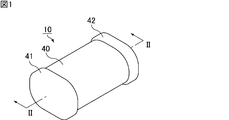
- FIG. 1 is a perspective view schematically showing an example of the film capacitor of the present invention.
- FIG. 2 is a sectional view taken along line II-II of the film capacitor shown in FIG.
- FIG. 3 is a perspective view schematically showing an example of a wound body of a metallized film constituting the film capacitors shown in FIGS. 1 and 2.
- the film capacitor of the present invention and the film for a film capacitor will be described.
- the present invention is not limited to the following configurations, and can be appropriately modified and applied without changing the gist of the present invention.
- a combination of two or more of the individual desirable configurations of the invention described below is also the invention.
- the film capacitor of the present invention includes a dielectric resin film and a metal layer provided on at least one surface of the dielectric resin film.
- the film capacitor of the present invention has, for example, a columnar column having an elongated cross section, and external terminal electrodes formed by, for example, metal spraying (metallic spraying) are provided at both ends in the direction of the central axis.
- a first dielectric resin film provided with a first metal layer and a second dielectric resin film provided with a second metal layer are laminated.
- a winding type film capacitor, which is wound in a wound state will be described as an example.
- the film capacitor of the present invention is a laminated type in which a first dielectric resin film provided with a first metal layer and a second dielectric resin film provided with a second metal layer are laminated. It may be a film capacitor or the like. Further, in the film capacitor of the present invention, a first dielectric resin film provided with a first metal layer and a second metal layer and a second dielectric resin film not provided with a metal layer are wound. It may be a film capacitor that has been rotated or laminated.
- FIG. 1 is a perspective view schematically showing an example of the film capacitor of the present invention.
- FIG. 2 is a sectional view taken along line II-II of the film capacitor shown in FIG.
- the film capacitor 10 shown in FIGS. 1 and 2 is a winding type film capacitor, and is a metallized film wound in a state in which a first metallized film 11 and a second metallized film 12 are laminated. 40, and a first external terminal electrode 41 and a second external terminal electrode 42 connected to both ends of the metallized film winding body 40 are provided.
- the first metallized film 11 is a first metal layer (counter electrode) provided on one surface of a first dielectric resin film 13 and a first dielectric resin film 13.
- the second metallized film 12 is a second metal layer (counter electrode) provided on one surface of the second dielectric resin film 14 and the second dielectric resin film 14. It has 16.
- the first metal layer 15 and the second metal layer 16 face each other with the first dielectric resin film 13 or the second dielectric resin film 14 interposed therebetween. Further, the first metal layer 15 is electrically connected to the first external terminal electrode 41, and the second metal layer 16 is electrically connected to the second external terminal electrode 42.
- the first dielectric resin film 13 and the second dielectric resin film 14 may have different configurations, but it is desirable that they have the same configuration.
- the first metal layer 15 is formed so as to reach one side edge on one surface of the first dielectric resin film 13 but not to the other side edge.
- the second metal layer 16 is formed so as not to reach one side edge on one surface of the second dielectric resin film 14, but to reach the other side edge.
- the first metal layer 15 and the second metal layer 16 are composed of, for example, an aluminum layer.
- FIG. 3 is a perspective view schematically showing an example of a wound body of a metallized film constituting the film capacitors shown in FIGS. 1 and 2.
- the end of the first metal layer 15 on the side reaching the side edge of the first dielectric resin film 13 and the second end of the second metal layer 16 The width of the first dielectric resin film 13 and the width of the second dielectric resin film 14 are such that the end portions on the side reaching the side edge of the dielectric resin film 14 are exposed from the laminated film.
- the layers are stacked so as to be shifted in the direction (left-right direction in FIG. 2).
- the wound body 40 of the metallized film is formed, and the first metal layer 15 and the second metal are formed.
- the layers 16 are held in a state of being exposed at the ends and are in a stacked state.
- the second dielectric resin film 14 is located outside the first dielectric resin film 13, and the first dielectric resin film 13 and the second dielectric resin film 14 are formed.
- Each of the first metal layer 15 and the second metal layer 16 is wound so as to face inward.
- the first external terminal electrode 41 and the second external terminal electrode 42 are formed by spraying, for example, zinc or the like onto each end surface of the wound body 40 of the metallized film obtained as described above. ..
- the first external terminal electrode 41 comes into contact with the exposed end of the first metal layer 15 and is thereby electrically connected to the first metal layer 15.
- the second external terminal electrode 42 comes into contact with the exposed end of the second metal layer 16 and is thereby electrically connected to the second metal layer 16.
- the wound body of the metallized film is pressed into a flat shape such as an ellipse or an oval, and has a more compact shape than when the cross-sectional shape is a perfect circle. ..
- the film capacitor of the present invention may include a cylindrical winding shaft.
- the winding shaft is arranged on the central axis of the metallized film in the wound state, and serves as a winding shaft when the metallized film is wound.
- examples of the metal contained in the metal layer include aluminum (Al), titanium (Ti), zinc (Zn), magnesium (Mg), tin (Sn), nickel (Ni) and the like. Be done.
- the thickness of the metal layer is not particularly limited, but is, for example, 5 nm or more and 40 nm or less.
- the thickness of the metal layer is specified by observing a cross section of a dielectric resin film provided with the metal layer cut in the thickness direction using an electron microscope such as a field emission scanning electron microscope (FE-SEM). can do.
- FE-SEM field emission scanning electron microscope
- the metal layer is provided with a fuse portion.
- the fuse portion means a portion where the metal layer serving as the counter electrode is divided into a plurality of electrodes and the electrode portion is connected to the electrode portion.
- the pattern of the metal layer having the fuse portion is not particularly limited, and for example, the electrode patterns disclosed in JP-A-2004-363431, JP-A-5-251266 and the like can be used.
- the film for the film capacitor of the present invention is used as the dielectric resin film.
- the film for a film capacitor of the present invention may be used for both the first dielectric resin film 13 and the second dielectric resin film 14.
- the film for a film capacitor of the present invention may be used for only one of them.
- the film for a film capacitor of the present invention comprises a cured product of a first organic material and a second organic material.
- the film for a film capacitor of the present invention is made of a cured product obtained by reacting a hydroxyl group (OH group) of a first organic material with an isocyanate group (NCO group) of a second organic material.
- the first organic material is composed of an organic polymer having a hydroxyl group and a benzene ring in a repeating unit.
- the first organic material is preferably made of a phenoxy resin.
- the second organic material consists of diphenylmethane diisocyanate, a modified diphenylmethane diisocyanate, or a mixture thereof.
- the second organic material is preferably composed of 4,4'-diphenylmethane diisocyanate, a modified 4,4'-diphenylmethane diisocyanate, or a mixture thereof.
- the film for a film capacitor of the present invention may contain at least one of a hydroxyl group and an isocyanate group.
- the film for a film capacitor of the present invention may contain either a hydroxyl group or an isocyanate group, or may contain both a hydroxyl group and an isocyanate group.
- FT-IR Fourier transform infrared spectrophotometer
- the coefficient of linear expansion at 40 ° C is ⁇ 40 ° C
- the coefficient of linear expansion at 80 ° C is ⁇ 80 ° C, 120 ° C.
- the coefficient of linear expansion is ⁇ 120 ° C.
- the value of ⁇ 40 ° C./ ⁇ 80 ° C. is 1.05 or more
- the value of ⁇ 80 ° C./ ⁇ 120 ° C. is 1.1 or more.
- the dielectric breakdown strength at 145 ° C. is 300 V / ⁇ m or more.
- the coefficient of linear expansion of the film is a value calculated from the rate of change in length from 0 ° C to each temperature of the film by the thermomechanical analysis (TMA) method.
- ⁇ 40 ° C./ ⁇ 80 ° C. is 1.05 or more.
- the value of ⁇ 40 ° C./ ⁇ 80 ° C. is, for example, 1.35 or less.
- ⁇ 80 ° C./ ⁇ 120 ° C. is 1.1 or more, preferably 1.15 or more.
- the value of ⁇ 80 ° C./ ⁇ 120 ° C. is, for example, 1.40 or less.
- ⁇ 40 ° C./ ⁇ 120 ° C. is not particularly limited, but is preferably 1.2 or more, and more preferably 1.25 or more. On the other hand, the value of ⁇ 40 ° C./ ⁇ 120 ° C. is, for example, 1.50 or less.
- the film for a film capacitor of the present invention may also contain an additive for adding other functions.
- smoothness can be imparted by adding a leveling agent.
- the additive is a material that has a functional group that reacts with a hydroxyl group and / or an isocyanate group and forms a part of the crosslinked structure of the cured product. Examples of such a material include a resin having at least one functional group selected from the group consisting of an epoxy group, a silanol group and a carboxyl group.
- the thickness of the film for a film capacitor of the present invention is not particularly limited, but if the film is too thin, it tends to become brittle. Therefore, the thickness of the film for a film capacitor of the present invention is preferably 1 ⁇ m or more, and more preferably 3 ⁇ m or more. On the other hand, if the film is too thick, defects such as cracks are likely to occur during film formation. Therefore, the thickness of the film for a film capacitor of the present invention is preferably 10 ⁇ m or less, and more preferably 5 ⁇ m or less.
- the thickness of the film means the thickness of the film alone, not including the thickness of the metal layer. The thickness of the film can be measured using an optical film thickness meter.
- the film for a film capacitor of the present invention is obtained by molding a resin solution containing a first organic material and a second organic material into a film, and then heat-treating and curing the resin solution.
- the resin solution is prepared, for example, by dissolving the above-mentioned first organic material and second organic material in a solvent, mixing them, and adding additives as necessary.
- the solvent contained in the resin solution may be present as a residue in the cured film.
- the weight ratio of the first organic material to the second organic material is preferably 50/50 or more and 75/25 or less.
- the solvent it is preferable to use a mixed solvent containing methyl ethyl ketone (MEK) and tetrahydrofuran (THF).
- MEK methyl ethyl ketone
- THF tetrahydrofuran
- the weight ratio of MEK to THF (MEK / THF) is preferably 15/85 or more and 85/15 or less.
- a metallized film is obtained by using the film for a film capacitor of the present invention as a dielectric resin film and forming a metal layer on one surface of the dielectric resin film.
- the method for forming the metal layer include a method such as thin film deposition.
- a laminated body is obtained by laminating two metallized films having a metal layer formed on one surface of a dielectric resin film in a state of being shifted by a predetermined distance in the width direction and then winding the film. If necessary, the laminate may be sandwiched from a direction perpendicular to the width direction and pressed into an elliptical cylinder shape.
- a film capacitor as shown in FIG. 1 can be obtained.
- thermal spraying can be mentioned.
- Example 1 As the first organic material, a phenoxy resin having a bisphenol A skeleton was prepared, and as the second organic material, a mixture of 4,4'-diphenylmethane diisocyanate (MDI) and a modified product thereof was prepared.
- MDI 4,4'-diphenylmethane diisocyanate
- the first organic material and the second organic material are dissolved in a mixed solvent of MEK and THF and mixed, and a silicone-based surface conditioner BYK370 (manufactured by Big Chemie Japan Co., Ltd.) is further added to the coating composition ( Resin solution) was prepared.
- the coating composition is coated on a polyethylene terephthalate (PET) film which is a base film, and after coating, a hot air of 70 ° C. is applied to dry the solvent, and then the coating composition is peeled off from the PET film to make the thickness. A 3 ⁇ m film was formed. The obtained film was heat-treated at 150 ° C. for 4 hours to cure.
- PET polyethylene terephthalate
- Example 1 As described above, the sample of Example 1 was prepared.
- Example 2 A sample was prepared in the same manner as in Example 1 except that the drying temperature of the solvent was changed from 70 ° C. to 100 ° C.
- Example 1 A sample was prepared in the same manner as in Example 1 except that the drying temperature of the solvent was changed from 70 ° C. to 140 ° C.
- Example 2 A sample was prepared in the same manner as in Example 1 except that the drying temperature of the solvent was changed from 70 ° C. to 180 ° C.
- the dielectric breakdown strength at 145 ° C. is 300 V. It was less than / ⁇ m.
- Film capacitor 11 First metallized film 12 Second metallized film 13 First dielectric resin film 14 Second dielectric resin film 15 First metal layer 16 Second metal layer 40 Metallic film Winding body 41 First external terminal electrode 42 Second external terminal electrode
Landscapes
- Engineering & Computer Science (AREA)
- Power Engineering (AREA)
- Microelectronics & Electronic Packaging (AREA)
- Manufacturing & Machinery (AREA)
- Fixed Capacitors And Capacitor Manufacturing Machines (AREA)
- Polyurethanes Or Polyureas (AREA)
Abstract
Condensateur à film (10) qui est pourvu : d'un film de résine diélectrique (par exemple, d'un premier film de résine diélectrique (13) qui est formé à partir d'un produit durci d'un premier matériau organique et d'un second matériau organique ; et d'une couche métallique (par exemple, une première couche métallique (15) qui est disposée sur au moins une surface du film de résine diélectrique. Le premier matériau organique est composé d'un polymère organique qui présente un groupe hydroxyle et un cycle benzène dans une unité répétitive. Le second matériau organique est composé de diisocyanate de diphénylméthane, d'un diisocyanate de diphénylméthane modifié ou d'un mélange de ceux-ci. Parmi les coefficients d'expansion linéaire du film décrit ci-dessus, sur la base de celui à 0 °C, si α40°C est le coefficient de dilatation linéaire à 40 °C, α80°C est le coefficient de dilatation linéaire à 80 °C et α120°C est le coefficient de dilatation linéaire à 120 °C, la valeur de α40°C/α80°C est de 1,05 ou plus, et la valeur α80°C/α120°C est de 1,1 ou plus.
Priority Applications (2)
| Application Number | Priority Date | Filing Date | Title |
|---|---|---|---|
| CN202080048023.3A CN114051648B (zh) | 2019-12-27 | 2020-12-22 | 薄膜电容器以及薄膜电容器用薄膜 |
| JP2021567490A JP7136369B2 (ja) | 2019-12-27 | 2020-12-22 | フィルムコンデンサ、及び、フィルムコンデンサ用フィルム |
Applications Claiming Priority (2)
| Application Number | Priority Date | Filing Date | Title |
|---|---|---|---|
| JP2019-237617 | 2019-12-27 | ||
| JP2019237617 | 2019-12-27 |
Publications (1)
| Publication Number | Publication Date |
|---|---|
| WO2021132257A1 true WO2021132257A1 (fr) | 2021-07-01 |
Family
ID=76572987
Family Applications (1)
| Application Number | Title | Priority Date | Filing Date |
|---|---|---|---|
| PCT/JP2020/047994 Ceased WO2021132257A1 (fr) | 2019-12-27 | 2020-12-22 | Condensateur à film et film pour condensateurs à film |
Country Status (3)
| Country | Link |
|---|---|
| JP (1) | JP7136369B2 (fr) |
| CN (1) | CN114051648B (fr) |
| WO (1) | WO2021132257A1 (fr) |
Families Citing this family (1)
| Publication number | Priority date | Publication date | Assignee | Title |
|---|---|---|---|---|
| US12456584B2 (en) | 2022-07-11 | 2025-10-28 | Rubycon Corporation | Thin film polymer laminated capacitor and manufacturing method therefor |
Citations (2)
| Publication number | Priority date | Publication date | Assignee | Title |
|---|---|---|---|---|
| WO2018142922A1 (fr) * | 2017-02-03 | 2018-08-09 | 株式会社村田製作所 | Condensateur à film, procédé de fabrication d'un condensateur à film, film de résine diélectrique et procédé de fabrication d'un film de résine diélectrique |
| WO2019097750A1 (fr) * | 2017-11-15 | 2019-05-23 | 株式会社村田製作所 | Condensateur à film et film métallisé |
Family Cites Families (6)
| Publication number | Priority date | Publication date | Assignee | Title |
|---|---|---|---|---|
| CN102034608B (zh) * | 2009-09-24 | 2014-12-17 | 日立Aic株式会社 | 金属化薄膜电容器 |
| JP5734069B2 (ja) * | 2011-04-13 | 2015-06-10 | 小島プレス工業株式会社 | フィルムコンデンサ素子及びフィルムコンデンサ並びにフィルムコンデンサ素子の製造方法 |
| CN104137203B (zh) | 2012-02-29 | 2017-04-05 | 株式会社村田制作所 | 薄膜电容器用电介质树脂组合物和薄膜电容器 |
| JP2016168833A (ja) * | 2015-03-12 | 2016-09-23 | 東レ株式会社 | 成型用積層フィルム及びそれを用いた成型品 |
| JP7278971B2 (ja) * | 2018-01-18 | 2023-05-22 | 日精エー・エス・ビー機械株式会社 | 容器 |
| EP3736841B1 (fr) | 2018-01-25 | 2025-12-17 | Murata Manufacturing Co., Ltd. | Condensateur à film, et boîtier extérieur pour condensateur à film |
-
2020
- 2020-12-22 WO PCT/JP2020/047994 patent/WO2021132257A1/fr not_active Ceased
- 2020-12-22 CN CN202080048023.3A patent/CN114051648B/zh active Active
- 2020-12-22 JP JP2021567490A patent/JP7136369B2/ja active Active
Patent Citations (2)
| Publication number | Priority date | Publication date | Assignee | Title |
|---|---|---|---|---|
| WO2018142922A1 (fr) * | 2017-02-03 | 2018-08-09 | 株式会社村田製作所 | Condensateur à film, procédé de fabrication d'un condensateur à film, film de résine diélectrique et procédé de fabrication d'un film de résine diélectrique |
| WO2019097750A1 (fr) * | 2017-11-15 | 2019-05-23 | 株式会社村田製作所 | Condensateur à film et film métallisé |
Also Published As
| Publication number | Publication date |
|---|---|
| CN114051648A (zh) | 2022-02-15 |
| CN114051648B (zh) | 2023-02-24 |
| JPWO2021132257A1 (fr) | 2021-07-01 |
| JP7136369B2 (ja) | 2022-09-13 |
Similar Documents
| Publication | Publication Date | Title |
|---|---|---|
| JP7268734B2 (ja) | フィルムコンデンサ、及び、フィルムコンデンサ用フィルム | |
| JP6944161B2 (ja) | フィルムコンデンサ及びフィルムコンデンサの製造方法 | |
| JP6677358B2 (ja) | フィルムコンデンサ、及び、フィルムコンデンサ用フィルム | |
| JP2021180336A (ja) | フィルムコンデンサ、フィルムコンデンサの製造方法、誘電体樹脂フィルム、及び、誘電体樹脂フィルムの製造方法 | |
| WO2017175511A1 (fr) | Condensateur à film, film pour condensateur et procédé de production de condensateur à film | |
| JP7180699B2 (ja) | フィルムコンデンサ、及び、フィルムコンデンサ用の誘電体樹脂フィルム | |
| CN111328424B (zh) | 薄膜电容器以及金属化薄膜 | |
| JP7234831B2 (ja) | フィルムコンデンサ用フィルム、フィルムコンデンサ用フィルムの製造方法、フィルムコンデンサ、及び、フィルムコンデンサの製造方法 | |
| WO2021132257A1 (fr) | Condensateur à film et film pour condensateurs à film | |
| JP7099636B2 (ja) | フィルムコンデンサ、及び、フィルムコンデンサ用フィルム | |
| WO2022065295A1 (fr) | Condensateur à film | |
| JP7525301B2 (ja) | フィルムコンデンサおよびフィルムコンデンサ用フィルム | |
| JP7348960B2 (ja) | フィルムコンデンサ、及び、フィルムコンデンサ用フィルム | |
| WO2023105990A1 (fr) | Condensateur à film et film de résine | |
| JP7200997B2 (ja) | フィルムコンデンサ、フィルムコンデンサ用フィルム及びフィルムコンデンサ用フィルムの製造方法 | |
| JP2021175564A (ja) | 樹脂シートの製造方法およびフィルムコンデンサの製造方法 | |
| JP2022045539A (ja) | フィルムコンデンサおよびフィルムコンデンサ用フィルム | |
| CN118318281A (zh) | 薄膜电容器 | |
| WO2023282077A1 (fr) | Condensateur à film | |
| JP2022045538A (ja) | フィルムコンデンサおよび樹脂フィルム |
Legal Events
| Date | Code | Title | Description |
|---|---|---|---|
| 121 | Ep: the epo has been informed by wipo that ep was designated in this application |
Ref document number: 20907495 Country of ref document: EP Kind code of ref document: A1 |
|
| ENP | Entry into the national phase |
Ref document number: 2021567490 Country of ref document: JP Kind code of ref document: A |
|
| NENP | Non-entry into the national phase |
Ref country code: DE |
|
| 122 | Ep: pct application non-entry in european phase |
Ref document number: 20907495 Country of ref document: EP Kind code of ref document: A1 |