WO2021182017A1 - 位置検出センサ及び位置検出センサの製法 - Google Patents
位置検出センサ及び位置検出センサの製法 Download PDFInfo
- Publication number
- WO2021182017A1 WO2021182017A1 PCT/JP2021/005392 JP2021005392W WO2021182017A1 WO 2021182017 A1 WO2021182017 A1 WO 2021182017A1 JP 2021005392 W JP2021005392 W JP 2021005392W WO 2021182017 A1 WO2021182017 A1 WO 2021182017A1
- Authority
- WO
- WIPO (PCT)
- Prior art keywords
- position detection
- base material
- terminal
- detection sensor
- conductors
- Prior art date
- Legal status (The legal status is an assumption and is not a legal conclusion. Google has not performed a legal analysis and makes no representation as to the accuracy of the status listed.)
- Ceased
Links
Images





Classifications
-
- G—PHYSICS
- G06—COMPUTING OR CALCULATING; COUNTING
- G06F—ELECTRIC DIGITAL DATA PROCESSING
- G06F3/00—Input arrangements for transferring data to be processed into a form capable of being handled by the computer; Output arrangements for transferring data from processing unit to output unit, e.g. interface arrangements
- G06F3/01—Input arrangements or combined input and output arrangements for interaction between user and computer
- G06F3/03—Arrangements for converting the position or the displacement of a member into a coded form
- G06F3/041—Digitisers, e.g. for touch screens or touch pads, characterised by the transducing means
- G06F3/046—Digitisers, e.g. for touch screens or touch pads, characterised by the transducing means by electromagnetic means
-
- G—PHYSICS
- G06—COMPUTING OR CALCULATING; COUNTING
- G06F—ELECTRIC DIGITAL DATA PROCESSING
- G06F3/00—Input arrangements for transferring data to be processed into a form capable of being handled by the computer; Output arrangements for transferring data from processing unit to output unit, e.g. interface arrangements
- G06F3/01—Input arrangements or combined input and output arrangements for interaction between user and computer
- G06F3/03—Arrangements for converting the position or the displacement of a member into a coded form
- G06F3/041—Digitisers, e.g. for touch screens or touch pads, characterised by the transducing means
- G06F3/0416—Control or interface arrangements specially adapted for digitisers
- G06F3/04164—Connections between sensors and controllers, e.g. routing lines between electrodes and connection pads
-
- G—PHYSICS
- G06—COMPUTING OR CALCULATING; COUNTING
- G06F—ELECTRIC DIGITAL DATA PROCESSING
- G06F2203/00—Indexing scheme relating to G06F3/00 - G06F3/048
- G06F2203/041—Indexing scheme relating to G06F3/041 - G06F3/045
- G06F2203/04102—Flexible digitiser, i.e. constructional details for allowing the whole digitising part of a device to be flexed or rolled like a sheet of paper
-
- G—PHYSICS
- G06—COMPUTING OR CALCULATING; COUNTING
- G06F—ELECTRIC DIGITAL DATA PROCESSING
- G06F2203/00—Indexing scheme relating to G06F3/00 - G06F3/048
- G06F2203/041—Indexing scheme relating to G06F3/041 - G06F3/045
- G06F2203/04103—Manufacturing, i.e. details related to manufacturing processes specially suited for touch sensitive devices
Definitions
- the present invention relates to a position detection sensor in which a plurality of electrode conductors are arranged on a base material in order to detect a position indicated by a position indicator, and a method for manufacturing the position detection sensor.
- Patent Document 1 Japanese Unexamined Patent Publication No. 2013-186784
- a plurality of electrode conductors are formed of copper on a sheet-like substrate or a film-like substrate.
- the foil pattern is formed as a predetermined pattern by printing or vapor deposition.
- Patent Document 2 Japanese Unexamined Patent Publication No. 7-253840 discloses a method for producing a position detection sensor at low cost. That is, in the method described in Patent Document 2, guide pins (pins for cloth wires) are arranged on a flat plate so that a predetermined electrode conductor pattern can be formed, and a coated conductor wire (insulation sensor) is provided. The wire) is hooked on the guide pin in sequence, and the wire is laid while being folded back to form an electrode conductor pattern.
- the position detection sensor of Patent Document 2 does not have a terminal portion, and the coated conductor wire constituting the electrode conductor is simply extended from the flat plate and led out as a lead portion. For this reason, in order to connect each of the plurality of electrode conductors of the position detection sensor to the external circuit, it is necessary to peel off the coated conductor of the lead portion and solder each of them, which is very troublesome. There was a problem that it was not suitable for mass production.
- a position detection sensor is provided so as to be superimposed on the display screen of the display for display so that the input operation on the display screen using the position indicator by the user can be detected by the position detection sensor.
- An input device is provided.
- the detection area of the position detection sensor is set to exactly overlap the display area of the display screen of the display so that the operation input in the entire display screen can be detected as the operation input. It is composed of. Then, in this type of input device, it is required to make the outer frame portion of the display screen as narrow as possible regardless of whether the display is large or small.
- the terminal portion since the terminal portion is formed on the same surface as the electrode conductor pattern, it exists outside the detection region including the region where the electrode conductor is formed. It will be. Therefore, the area of the terminal portion exists outside the detection area of the position detection sensor, which is the same size as the display screen of the display, and the size of the outer frame portion of the display screen is corresponding to the area of the terminal portion. There is a problem that the size becomes large.
- An object of the present invention is to provide a position detection sensor capable of solving the above problems.
- each of the plurality of electrode conductors made of coated conductors is allowed to overlap with each other so as to form a predetermined pattern.
- the material is adhered and disposed with an adhesive, and the ends of the coated conductors of the plurality of electrode conductors are aligned so as to be connectable to the corresponding terminal conductors of the terminal portions.
- the arranged sensor pattern part and With A bent region is formed between the region of the terminal portion and the region of the sensor pattern portion on the one surface of the base material.
- each of the plurality of electrode conductors in the bent region is arranged in an extendable state between the terminal portion and the sensor pattern portion.
- the position detection sensor since a bending region exists between the terminal portion formed on one surface of the base material made of a bendable material and the sensor pattern portion, the position detection sensor is bent in the bending region to form a terminal.
- the portion can be located on the side opposite to the one side of the base material.
- one side of the equipment can be substantially limited to the area of the sensor pattern portion, and when the position detection sensor is arranged so as to be superimposed on the display screen of the display for display, the size of the outer frame portion thereof. Can be narrowed.
- each end of the plurality of electrode conductors of the sensor pattern portion is usually extended to the terminal portion via the bent region so as to be electrically connected, but the bent region of the electrode conductor is formed. If there is no room in the upper stretched portion, the bending stress generated when the terminal portion is bent to the side opposite to the one surface side of the base material causes the electrical connection between the end portion of the electrode conductor and the terminal portion. May become defective or the electrode conductor may break.
- each of the plurality of electrode conductors in the bent region is arranged in an extendable state between the terminal portion and the sensor pattern portion, the electrode conductors There is a margin in the stretched portion on the bent region, and the bending stress generated when the terminal portion is bent to the side opposite to the one surface side of the base material causes a poor electrical connection between the end portion of the electrode conductor and the terminal portion. It is possible to prevent the electrode conductor from becoming broken or breaking.
- FIG. 1 shows the flowchart for demonstrating the flow of an example of the manufacturing method of the embodiment of the position detection sensor by this invention. It is a figure used for demonstrating an example of the manufacturing method of the Embodiment of the position detection sensor by this invention. It is a figure used for demonstrating an example of the manufacturing method of the Embodiment of the position detection sensor by this invention. It is a figure for demonstrating the structural example of another embodiment of the position detection sensor by this invention. It is a figure used for demonstrating the manufacturing method of another embodiment of the position detection sensor by this invention.
- the embodiment of the position detection sensor described below is an electromagnetic induction type position detection sensor, and each pattern of the plurality of electrode conductors constituting the sensor pattern portion is a loop coil pattern.
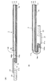
- FIG. 1 is a diagram for explaining the configuration of the position detection sensor 1 of this embodiment, and FIG. 1 (A) shows a surface on which the sensor pattern portion of the position detection sensor 1 is formed orthogonal to the surface.
- FIG. 1 (B) is a conceptual diagram of a cross-sectional structure of the position detection sensor 1.
- a rectangular sheet-like or film-like substrate made of a bendable insulating material, for example, PET (Polyethylene terephthalate).
- a sensor pattern portion 13 composed of a plurality of loop coils as a plurality of electrode conductors is adhered and arranged on one surface 11a of the (board) 11 by an adhesive material 12.
- a flexible substrate can be used as the base material 11.
- the sensor pattern portion 13 occupies most of the vertical direction on one surface 11a of the rectangular base material 11, and is a rectangular region ARa excluding the left side portion in the horizontal direction of the base material 11. ..
- a space air layer
- the protective sheet 14 is provided to the base material 11 by the adhesive material 12 via the space portion of the sensor pattern portion 13. It is glued and joined.
- the terminal portion 16 is provided via the adhesive 15 at the lateral end portion of the lateral left portion on the one surface 11a of the base material 11 where the sensor pattern portion 13 is not arranged. It is adhered. That is, the terminal portion 16 is provided in the region ARb of the lateral edge portion of the base material 11 which does not overlap with the region ARa in which the sensor pattern portion 13 is arranged.
- the terminal portion 16 is used for electrical connection with each of a plurality of electrode conductors of the sensor pattern portion 13 on a sheet-like or film-like substrate made of an insulating material, for example, PET.
- the terminal conductor 17 made of a copper foil pattern is formed by, for example, printing.
- the region between the region ARa of the sensor pattern portion 13 and the region ARb of the terminal portion 16 is a bending region ARc.
- the upper part of the region ARb and the bent region ARc of the terminal portion 16 is not covered with the protective sheet 14.
- the bent region ARc is not coated with the adhesive material 15.
- the lateral length of the base material 11 of the bent region ARc is such that the terminal portion 16 side is the base material 11 from the vicinity of the lateral end of the region ARa of the sensor pattern portion 13 of the bent region ARc. The length is selected so that it can be bent so as to be located on the side opposite to the one side 11a side.
- the sensor pattern unit 13 is composed of a plurality of loop coils as an example of a plurality of electrode conductors.
- the plurality of loop coils are composed of a plurality of X-axis direction loop coils 13X and a plurality of Y-axis direction loop coils 13Y.
- the X-axis direction loop coil 13X is composed of a rectangular loop coil whose long side direction is the vertical direction (Y-axis direction of position coordinates) of the base material 11, and a plurality of the X-axis direction loop coils 13X are the base materials. 11 are arranged and arranged at predetermined intervals in the lateral direction (X-axis direction of position coordinates). Further, the Y-axis direction loop coil 13Y is composed of a rectangular loop coil whose long side direction is the lateral direction of the base material 11, and the Y-axis direction loop coils are arranged in the vertical direction of the base material 11 at predetermined intervals. And arranged.
- each of the plurality of X-axis direction loop coils 13X and the plurality of Y-axis direction loop coils 13Y constituting the sensor pattern portion 13 is allowed to overlap with each other by the coated conductors 18, and is a base material. It is arranged on one side 11a of 11.
- each of the X-axis direction loop coil 13X and the Y-axis direction loop coil 13Y is located at a predetermined position on one surface 11a of the base material 11 in this embodiment, as shown in FIG. 1 (A). , They are arranged so as to have a predetermined pattern.
- the ends 18E of each of the X-axis direction loop coil 13X and the Y-axis direction loop coil 13Y are located on the lateral terminal portion 16 side of the region ARa of the sensor pattern portion 13 as shown in FIG.
- the terminal portion 16 At the edge of the terminal portion 16, it is arranged so as to extend laterally from the protective sheet 14 toward the terminal portion 16 side and extend to the region ARb of the terminal portion 16 so as to straddle the bent region ARc.
- the derivation positions of the both end portions 18E of the X-axis direction loop coil 13X and the Y-axis direction loop coil 13Y from the sensor pattern portion 13 are preliminarily assumed that the both end portions 18E of the terminal portion 16 should be connected. It is aligned so as to match the defined position of the corresponding terminal conductor 17.
- both end portions 18E of the X-axis direction loop coil 13X and the Y-axis direction loop coil 13Y straddle the bending region ARc from the end edge of the sensor pattern portion 13 on the lateral terminal portion 16 side of the region ARa.
- it When it is linearly extended in the direction, it is configured to be in a state of being just positioned on the corresponding terminal conductor 17 of the terminal portion 16.
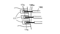
- the insulating coating of the coated conductor 18 is peeled off from the tip portions 18Ea of both end portions 18E of the X-axis direction loop coil 13X and the Y-axis direction loop coil 13Y.
- the lead wire is exposed, and the tip portion 18Ea from which the lead wire is exposed is located on the terminal conductor 17 of the terminal portion 16.
- each of the terminal conductors 17 of the terminal portion 16 and the tip portions 18Ea of both end portions 18E of the X-axis direction loop coil 13X and the Y-axis direction loop coil 13Y are soldered, for example. It is electrically connected.
- each of the terminal conductors 17 of the terminal portion 16 is preliminarily filled with solder, and the terminal 18Ea at both ends 18E of each of the X-axis direction loop coil 13X and the Y-axis direction loop coil 13Y is located.
- each of the terminal conductors 17 of the terminal portion 16 and the tip portions 18Ea of both end portions 18E of the X-axis direction loop coil 13X and the Y-axis direction loop coil 13Y are formed. Is soldered.
- a metal sheet 19 as an example of the electromagnetic shield layer is adhered so as to cover the entire surface opposite to one surface 11a of the base material 11.
- the metal sheet 19 is composed of an aluminum sheet and an amorphous sheet.
- the amorphous sheet of the metal sheet 19 prevents the electromagnetic waves radiated from the sensor pattern portion 13 from being emitted to the outside on the side opposite to the one side 11a of the base material 11, and the aluminum sheet is opposite to the one side 11a of the base material 11. It plays a role of preventing noise from the outside on the side from being mixed into the sensor pattern portion 13.
- the metal sheet 19 does not cover the entire surface of the base material 11 opposite to the one surface 11a, but the sensor pattern portion 13 of the surface of the base material 11 opposite to the one surface 11a.
- the coating may be applied so as to cover only the region on the back side of the region ARa.
- the coated lead wire 18 is used to form the sensor pattern portion 13 including the X-axis direction loop coil 13X and the Y-axis direction loop coil 13Y, and this sensor pattern is formed.
- the portion 13 is fixed between the base material 11 and the protective sheet 14 by the adhesive material 12. Therefore, the position detection sensor 1 can be manufactured at low cost.
- the terminal portion 16 on which the terminal conductor 17 is formed in advance is formed on one surface 11a of the base material 11, and the loop coil of the sensor pattern portion 13 is covered.
- the tips 18Ea of both ends 18E of the conductor 18 are aligned so that they can be connected to the corresponding terminal conductor 17 of the terminal 16, for example, by soldering, the corresponding terminal conductor 17 of the terminal 16. Can be easily electrically connected to each of the above.
- the position detection sensor 1 of this embodiment has an electrode conductor formed by using the coated conductor 18, and can provide a position detection sensor having an inexpensive and simple structure, and can be connected to an external circuit. By using the terminal portion 16, it becomes very easy.
- the circuit board 22 is connected to the terminal portion 16 via the flexible board 21.
- the flexible substrate 21 is formed with a conductive pattern 21a that is electrically connected to each of the terminal conductors 17 of the terminal portion 16, and one end side of the conductive pattern 21a is the terminal conductor 17 of the terminal portion 16. The other end is electrically connected to each of the terminal conductors (not shown) of the connector terminal portion of the circuit board 22.
- a position detection circuit as described later is formed on the circuit board 22.
- FIGS. 2A and 2B in the position detection sensor 1, the base material 11 is bent at the position of the bending region ARc on the side opposite to the one side 11a side, and in this example, the terminal portion 16.
- the flexible substrate 21 and the circuit substrate 22 are configured to be located on the side opposite to the one side 11a side of the substrate 11.
- FIG. 2A is a diagram for clarifying the bent state of the position detection sensor 1 shown in FIG. 2B, which is the same as FIG. 1B.
- the region ARb and the bent region ARc of the terminal portion 16 of the base material 11 are located on the side opposite to the one side 11a side of the base material 11, and the one side 11a side of the base material 11 is substantially a sensor. Only the pattern portion 13 can be occupied. Therefore, it is possible to reduce the size of the frame region when the position detection sensor 1 of this embodiment is superposed on the display screen of the display device and arranged.
- both end portions 18E of the X-axis direction loop coil 13X and the Y-axis direction loop coil 13Y of the sensor pattern portion 13 are extended to the region ARb of the terminal portion 16 via the bending region ARc, and the terminals are terminal. It is electrically connected to the unit 16.
- both end portions 18E of the X-axis direction loop coil 13X and the Y-axis direction loop coil 13Y are linearly extended to the region ARb of the terminal portion 16 via the bending region ARc, There is no margin in the stretched portion of both end portions 18E in the bending region ARc, and the bending stress generated when the terminal portion 16 is bent to the side opposite to the one surface 11a side of the base material 11 causes the tip portions 18Ea of both end portions 18E to be separated from each other. There is a risk that the electrical connection of the terminal portion 16 with the terminal conductor 17 will be poor, or that the coated conductor 18 will be broken.
- both end portions 18E of the X-axis direction loop coil 13X and the Y-axis direction loop coil 13Y are arranged so as to linearly connect the sensor pattern portion 13 and the terminal portion 16. Instead of providing it, it is arranged so as to be in an extendable state in the bent region ARc between the terminal portion 16 and the sensor pattern portion 13.
- each end portion 18E of the X-axis direction loop coil 13X and the Y-axis direction loop coil 13Y is a bending region.
- the ARc is configured to include a margin portion composed of a non-linear portion, and is arranged so as to be in an extendable state in the bent region ARc.
- the coated conductors 18 at both ends 18E of the X-axis direction loop coil 13X and the Y-axis direction loop coil 13Y in the bending region ARc are coiled once or a plurality of times. It is composed of winding margin portions 18Eb and 18Ec wound in a shape.
- the winding margin portions 18Eb and 18Ec have a coated lead wire on the guide pin used when patterning the X-axis direction loop coil 13X and the Y-axis direction loop coil 13Y on the sensor pattern portion 13, as will be described later. It is formed by wrapping it.
- both end portions 18E of the X-axis direction loop coil 13X and the Y-axis direction loop coil 13Y in the bending region ARc are in a state in which they can be extended in the bending region ARc between the terminal portion 16 and the sensor pattern portion 13. It is molded and arranged so as to have winding margin portions 18Eb and 18Ec.
- the base material 11 of the position detection sensor 1 of this embodiment is bent at the position of the bending region ARc to the side opposite to the one surface 11a side of the base material 11, the X-axis direction loop in the bending region ARc
- the coated conductors 18 at both ends 18E of the coil 13X and the Y-axis direction loop coil 13Y have a margin for bending stress due to the presence of the winding margins 18Eb and 18Ec, and the tip 18Ea and the terminal portion of both ends 18E are provided. It is possible to prevent the electrical connection with the terminal conductor 17 of 16 from becoming defective and the coated conductor 18 from being broken.
- the pen-type position indicator 3 used together with the position detection sensor 1 of this embodiment includes a coil 31 and a capacitor 32 connected in parallel to the coil 31. It has a built-in resonance circuit.
- X-axis direction loop coil 13X is, n arranged in the X-axis direction (n is an integer of 2 or more) has become the loop coils 13X 1 ⁇ 13X n rectangular present, Further, the loop coil 13Y in the Y-axis direction is composed of m (m is an integer of 2 or more) loop coils 13Y 1 to 13Y m arranged in the Y-axis direction.
- the position detection circuit 200 includes the selection circuit 201, the oscillator 202, the current driver 203, the transmission / reception switching circuit 204, the reception amplifier 205, the instruction position detection circuit 206, and the processing control unit 207. It is configured with.
- the selection circuit 201 sequentially selects one of the plurality of X-axis direction loop coils 13X and the plurality of Y-axis direction loop coils 13Y, and the selected loop coil is used with respect to the position indicator 3. The signal is transmitted and the signal returned from the position indicator 3 is received.
- a transmission / reception switching circuit 204 which is switched and controlled by the processing control unit 207, is connected to the selection circuit 201.
- the transmission / reception switching circuit 204 is connected to the transmission side terminal T, an AC signal is supplied from the oscillator 202 to the selection circuit 201, and when the transmission / reception switching circuit 204 is connected to the reception side terminal R, the signal from the selection circuit 201 is the reception amplifier 205. It is supplied to the indicated position detection circuit 206 through.
- the indicated position detection circuit 206 detects the induced voltage generated in the loop coil of the position detection sensor 1, that is, the received signal, converts the detected output signal into a digital signal, and outputs the detected output signal to the processing control unit 207.
- the processing control unit 207 positions the indicated positions in the X-axis direction and the Y-axis direction of the position indicator 3 based on the digital signal from the indicated position detection circuit 206, that is, the level of the voltage value of the induced voltage generated in each loop coil. Calculate the coordinate values.
- FIG. 4 is a diagram showing a configuration example of a manufacturing apparatus for a position detection sensor that executes the manufacturing method of this embodiment.
- the manufacturing apparatus for the position detection sensor in this example includes a wiring supply unit 100, a pretreatment unit 110, and a wiring unit 120.
- the wiring unit 120 includes a workbench 121 for forming the position detection sensor 1 and a biaxial mobile wiring device 122 provided on the workbench 121.
- the two-axis moving wiring device 122 has a moving bridge 1221 that slides in the X-axis direction of the position detection sensor 1 (see the direction of the arrow Ax in FIG. 3) and a Y-axis direction of the position detection sensor 1 (the direction of the arrow in FIG. 3). It is provided with a wiring nozzle mechanism 1222 that slides and moves in the direction of Ay).
- the moving bridge 1221 is a bridge that bridges the position detection sensor 1 between the two legs 1221a and 1221b and the two legs 1221a and 1221b in the direction along the Y-axis direction. It is provided with an entangled portion 1221c.
- the two legs 1221a and 1221b of the moving bridge 1221 are mounted on the workbench 121 on the two rails 121a and 121b provided in the X-axis direction, respectively. While the bridge entanglement portion 1221c is maintained in a state parallel to the Y-axis direction, the bridge entanglement portion 1221c is guided by the two rails 121a and 121b and slides in the X-axis direction.
- the wiring nozzle mechanism 1222 is movably attached to the bridging portion 1221c of the moving bridge 1221 in the bridging direction (Y-axis direction of the position detection sensor 1 (see the direction of the arrow direction Ay in FIG. 4)). There is. A wiring nozzle 1222a is attached to a portion of the wiring nozzle mechanism 1222 facing the surface of the workbench 121. The wiring nozzle 1222a feeds the coated conductor wire pretreated by the pretreatment unit 110 to the outside from its injection port.
- the wiring nozzle 1222a is caused by the sliding movement of the moving bridge 1221 in the biaxial moving wiring device 122 in the X-axis direction and the sliding movement of the wiring nozzle mechanism 1222 in the Y-axis direction. It is possible to move in any direction on the dimensional plane.
- the two-axis moving wiring device 122 includes a movement control unit (not shown in FIG. 4), which allows the moving bridge 1221 to slide in the X-axis direction and the wiring nozzle mechanism 1222 to slide in the Y-axis direction. It is configured to control dynamic movement. Then, in this embodiment, the movement control unit moves the wiring nozzle 1222a so as to dispose of each of the plurality of X-axis direction loop coils 13X and each of the plurality of Y-axis direction loop coils 13Y.
- the locus information is stored in advance.
- the movement control unit of the biaxially moving wiring device 122 controls the sliding movement of the moving bridge 1221 in the X-axis direction and the sliding movement of the wiring nozzle mechanism 1222 in the Y-axis direction based on the stored information. Then, the wiring nozzle 1222a is moved and controlled so as to dispose each of the plurality of X-axis direction loop coils 13X and each of the plurality of Y-axis direction loop coils 13Y.
- the workbench 121 of the wiring unit 120 has a pin table 123 provided with guide pins for guiding the X-axis direction loop coil 13X and the Y-axis direction loop coil 13Y so as to be formed as a pattern by coated conductors. It is provided.
- FIG. 5 is a diagram for explaining a configuration example of the pin table 123.
- the pin table 123 includes a guide pin mounting plate 1231, an intermediate plate 1232, and a release sheet 1233.
- the pin table 123 is configured by connecting the guide pin mounting plate 1231, the intermediate plate 1232, and the release sheet 1233 as shown in the lower part of FIG.
- the lower view of the pin table 123 in FIG. 5 is an enlarged view of the corresponding area of the area surrounded by the dotted line in the upper view of FIG.
- the guide pin mounting plate 1231 is guided so as to form each of the plurality of X-axis direction loop coils 13X and each of the plurality of Y-axis direction loop coils 13Y by the coated conductors discharged from the wiring nozzle 1222a.
- a large number of guide pins 124 are attached.
- the guide pins 124 are shown to be attached only to the ends of the guide pin mounting plates 1231 for illustration purposes, but in practice at least a plurality of X-axis direction loops. It is provided at each of the point positions where each of the coils 13X and the plurality of Y-axis direction loop coils 13Y are bent.
- the intermediate plate 1232 is provided between the guide pin mounting plate 1231 and the release sheet 1233, and as shown in FIG. 5, a position corresponding to each of the guide pins 124 provided on the guide pin mounting plate 1231.
- a through hole 125 is formed in the hole 125.
- the release sheet 1233 is provided on the intermediate plate 1232 attached to the guide pin mounting plate 1231. At this time, the guide pin 124 pierces the release sheet 1233, and the tip of the guide pin 124 protrudes onto the release sheet 1233. In this example, the tip of the guide pin 124 is sharpened like a needle.
- the guide pin mounting plate 1231, the intermediate plate 1232, and the release sheet 1233 are joined as shown in the lower part of FIG. 5, and a large number of guide pins 124 are planted at predetermined positions.
- the pin table 123 is configured.
- the plurality of X-axis direction loop coils 13X and the plurality of Y-axis direction loop coils 13Y are respectively provided by the coated conductors drawn from the wiring nozzle 1222a of the wiring nozzle mechanism 1222. Is formed as a predetermined loop coil pattern, and the sensor pattern portion 13 is formed.
- the surface of the release sheet 1233 is processed so that the formed sensor pattern portion 13 can be easily peeled off from the pin table 123.
- the position detection sensor 1 is manufactured by the procedure as described below by using the position detection sensor manufacturing device having the above configuration.
- the position detection sensor manufacturing apparatus of FIG. 4 uses a sequence control unit (not shown) to sequence control the operations of the wiring supply unit 100, the preprocessing unit 110, and the wiring unit 120 to control the position detection sensor 1. Perform manufacturing.
- the guide pins of the pin table 123 required to form one Y-axis direction loop coil 13Y and X-axis direction loop coil 13X.
- the arrangement positions of 124 and the pattern generation of their loop coils 13Y and 13X will be described with reference to FIG.
- the bent region ARc is provided with guide pins 124g and 124h for forming the winding margin portions 18Eb and 18Ec as an example of the margin portion composed of the non-linear portion.
- the coated conductor 18 is laid around the guide pins 124a to 124d and 124e, 124f as shown in FIG. 6, so that the region ARa of the sensor pattern portion 13 has a rectangular Y-axis direction loop coil. 13Y is formed, and both ends 18E of the coated conductor 18 of the Y-axis direction loop coil 13Y extending from the region ARa of the sensor pattern portion 13 to the region ARb of the terminal portion 16 via the bending region ARc are formed. ..
- both end portions 18E of the Y-axis direction loop coil 13Y are composed of one end portion 18Es and the other end portion 18Et, and the lead-out position of one end portion 18Es is the terminal portion. It is set to the position of the corresponding terminal conductor 17 of 16. Therefore, it is possible to connect the terminal conductor 17 of the terminal portion 16 by extending the one end portion 18Es of both end portions 18E of the Y-axis direction loop coil 13Y in a straight line across the bending region ARc. It becomes.
- the one end 18Es is not arranged in a straight line, but as shown in FIG. 6, once or a plurality of times with respect to the guide pin 124 g of the bending region ARc. It is configured to have a winding margin portion 18Eb configured by being wound.
- the other end portion 18Et of both end portions 18E of the Y-axis direction loop coil 13Y is also configured to be wound once or a plurality of times with respect to the guide pin 124h of the bending region ARc. It is configured to have a winding margin portion 18Ec.
- each of the other end portions 18Et of both end portions 18E of the plurality of Y-axis direction loop coils 13Y are connected in common to each other to form a ground wire portion GD, and FIG. As shown in A), it is connected to the terminal conductor connected to the ground electrode of the terminal portion 16.
- the winding margin portion 18Ec of the other end portion 18Et is formed between the lead-out position from the sensor pattern portion 13 and the ground wire portion GD in the bending region ARc.
- the region ARa of the sensor pattern portion 13 of the base material 11 of the pin table 123 corresponds to a vertically long rectangular shape.
- the coated conductor 18 is laid around the guide pins 124i to 124l and 124m, 124n as shown in FIG. 6, so that the rectangular X-axis direction loop coil 13X is formed in the region ARa of the sensor pattern portion 13.
- both end portions 18E of the coated conductor 18 of the X-axis direction loop coil 13X extending from the region ARa of the sensor pattern portion 13 to the region ARb of the terminal portion 16 via the bent region ARc are formed.
- the lead-out position of one end 18Es of both ends 18E of the X-axis direction loop coil 13X is set to the position of the corresponding terminal conductor 17 of the terminal portion 16.
- one end 18Es and the other end 18Et of both ends of the X-axis direction loop coil 13X are guide pins 124o of the bending region ARc as shown in FIG. And 124p are configured to have a winding margin portion 18Eb and a winding margin portion 18Ec that are wound once or a plurality of times, respectively.
- the winding margin portions 18Eb and 18Ec formed at both ends 18E of the Y-axis direction loop coil 13Y and the X-axis direction loop coil 13X are from the guide pins 124g, 124h, 124o, 124p.
- it When it is pulled out, it becomes an air-core coil and acts as a margin portion that can be extended and displaced in the lateral direction of the base material 11. Therefore, as described above, when the base material 11 is bent in the bending region ARc, it becomes an extension margin portion of the coated conducting wire 18, and the above-mentioned problems due to bending stress can be prevented.
- the sequence control unit instructs the wiring supply unit 100 to feed the coated conductor 18 to the pretreatment unit 110 (step S101).
- the coated lead wire 18 from the wiring supply unit 100 is cut to a length suitable for each of the X-axis direction loop coil 13X or the Y-axis direction loop coil 13Y, and the X-axis direction loop coil 13X or the X-axis direction loop coil 13X or Pretreatment is performed to expose the lead wire by peeling off the coating on the tip portion 18Ea of both end portions 18E of the Y-axis direction loop coil 13Y.
- the pretreatment unit 110 sends the pretreated covered conducting wire 18 to the wiring nozzle mechanism 1222 of the wiring unit 120 (step S102).
- the wiring unit 120 moves and controls the wiring nozzle 1222a of the wiring nozzle mechanism 1222 by the movement control unit of the two-axis moving wiring device 122, so that the coated conductor 18 is hooked on the guide pin on the pin table 123 and is X-axis.
- Each of the directional loop coil 13X and the Y-axis direction loop coil 13Y is formed, and at both ends 18E of each of the X-axis direction loop coil 13X and the Y-axis direction loop coil 13Y, a margin portion in the bending region ARc, in this example, a margin portion. ,
- the winding margin portions 18Eb and 18Ec are formed (step S103).
- the tips 18Ea of both ends 18E of the X-axis direction loop coil 13X and the Y-axis direction loop coil 13Y from which the coating of the coated lead wire 18 is peeled off to expose the lead wire are pins as shown in FIG.
- the base material 11 is made to protrude from the table 123 in the lateral direction (X-axis direction). Then, the positions of the tip portions 18Ea of the both end portions 18E are guided by the guide pins 124 and the coated conducting wires 18 are arranged, so that the terminal portions 16 correspond to the positions as shown in the above-described explanation of FIG. It is in a aligned state so that it is located on the terminal conductor 17.
- the sequence control unit sets the plurality of X-axis direction loop coils 13X and the plurality of Y-axis direction loops on the pin table 123.
- it is determined whether or not the sensor pattern portion 13 is completed it is determined whether or not the sensor pattern portion 13 is completed (step S104).
- step S104 the sequence control unit returns the process to step S101 and returns the processing to the plurality of X-axis direction loop coils 13X or the plurality of Y-axis direction loop coils.
- Each of the 13Ys is controlled so as to perform the same processing as in steps S101 to S103.
- step S104 When it is determined in step S104 that the sensor pattern portion 13 is completed, as shown in FIG. 8, the base material is placed on the sensor pattern portion 13 on the pin table 123 via, for example, an adhesive material 12 made of double-sided tape. 11 is aligned and pressed so that the sensor pattern portion 13 on the pin table 123 is adhered to the base material 11 by the adhesive material 12 (step S105).
- a terminal portion 16 on which a plurality of terminal conductors 17 (omitted in FIG. 8, see FIG. 1) is formed is formed on the surface 11a of the base material 11 facing the pin table 123. , Pre-adhered and formed.
- the base material 11 has a region ARb in which the terminal portion 16 is formed, a bent region ARc, and a region ARa of the sensor pattern portion (region shown by a dotted line in FIG. 8). See).
- the double-sided tape constituting the adhesive 12 has a size corresponding to the size of the region ARa of the sensor pattern portion 13, and in this example, the region ARb and the bent region where the terminal portion 16 is formed.
- the adhesive 12 is positioned on the ARc so as not to be present.
- the base material 11 is positioned so that the sensor pattern portion 13 of the pin table 123 corresponds to the region ARa of the sensor pattern portion 13, and is pressed onto the pin table 123 via the adhesive material 12.
- Positioning of the double-sided tape and the base material 11 as the adhesive 12 is performed by a predetermined guide pin 124 (for example, one corresponding to the four corner positions of the region ARa) protruding on the pin table 123.
- the adhesive material 12 may be adhered to the region ARa of the base material 11 in advance.
- both end portions 18E of the plurality of X-axis direction loop coils 13X or the plurality of Y-axis direction loop coils 13Y are on the bending region ARc.
- the bent region from the region ARa of the sensor pattern portion 13 so that the tip portion 18Ea exposed to the conductors of the both end portions 18E is connected to each of the corresponding terminal conductors 17 of the terminal portion 16. It is in a state of protruding in the direction of the terminal portion 16 across the ARc.
- the guide pin 124 When the one side 11a side of the base material 11 is pressed against the pin table 123 in the aligned state as described above, the guide pin 124 is in a state of penetrating the base material 11 and piercing the pin table 123.
- the portion 13 is in a state of being adhered to the ARa of the base material 11 by the adhesive material 12.
- the coatings of the coated conductors 18 of each of the plurality of X-axis direction loop coils 13X or the plurality of Y-axis direction loop coils 13Y are peeled off to expose the conductors at both ends 18E.
- the tip portion 18Ea is in a state of being located on the corresponding terminal conductor 17 of the terminal portion 16.
- the base material 11 is peeled off from the pin table 123 (step S106).
- the base material 11 is lifted from the guide pin 124 together with the intermediate plate 1232 and the release sheet 1233 by a lifting mechanism using a robot hand or the like, which is not shown. Be removed.
- the guide is held in a state where the base material 11 is held together with the intermediate plate 1232 and the release sheet 1233 by a robot hand or the like (not shown).
- the pin mounting plate 1231 may be removed from the base material 11 from the guide pin 124 by lowering it downward by the height of the guide pin or more.
- the base material 11 with the release sheet 1233 removed from the guide pin 124 is turned upside down and placed on a mounting table (not shown) different from the pin table 123. Then, the release sheet 1233 is peeled off from the sensor pattern portion 13 that is adhered to one surface 11a of the base material 11.
- the sensor pattern portion 13 is adhered to one surface 11a of the base material 11 removed from the pin table 123, and as described above, a plurality of X-axis direction loop coils 13X or a plurality of X-axis direction loop coils 13X.
- the tip portion 18Ea of each end portion 18E of each of the Y-axis direction loop coils 13Y, in which the coating of the coated conductor 18 is peeled off and the conductor is exposed, is located on the corresponding terminal conductor 17 of the terminal portion 16. It has become.
- solder 17a is preliminarily piled up on each terminal conductor 17 of the terminal portion 16 on one surface 11a of the base material 11. Then, in this embodiment, by heating the solder 17a portion of each terminal conductor 17 of the terminal portion 16, the solder 17a is melted, the coating of the coated conductor 18 is peeled off, and both ends where the conductor is exposed. The tip portion 18Ea of 18E is soldered to the corresponding terminal conductor 17 of the terminal portion 16 and electrically connected (step S107).
- the protective sheet 14 (see FIG. 1) is adhered and covered with an adhesive on the sensor pattern portion 13 of the region ARa of the one surface 11a of the base material 11 (step S108).
- the metal sheet 19 constituting the electromagnetic shield layer is adhered to the surface of the base material 11 opposite to one surface 11a (step S109).
- the flexible substrate 21 is connected to the terminal portion 16 so that each of the terminal conductors 17 of the terminal portion 16 and the terminal portion of the circuit board 22 are connected (step S110).
- the position detection sensor 1 of this embodiment can be manufactured. Then, when the position detection sensor 1 of this embodiment is superimposed on the display screen of the input device, for example, and arranged on the back side of the display screen, the position detection sensor 1 has the bending region ARc as described above. Bend it at the place and arrange it.
- the adhesive material for attaching the protective sheet 14 may be used separately from the adhesive material 12, or the adhesive material 12 (of the sensor pattern portion 13) existing in a portion other than the sensor pattern portion 13.
- the adhesive material 12) in the region where the coated conductive wire forming the loop coil pattern does not exist may be used for adhering the protective sheet 14 to one surface 11a of the base material 11.
- the sensor pattern portion 13 is easily arranged on one surface 11a of the base material by using the coated conductor wire, and the terminal conductor 17 of the terminal portion 16 is provided. And, it is possible to manufacture the position detection sensor 1 which can be easily electrically connected to each loop coil of the sensor pattern unit 13. Then, by using the manufacturing method of this embodiment, mass production of the position detection sensor 1 becomes possible.
- margin portion formed by the non-linear portion of the coated conductor in the bent region ARc is wound around both ends 18E of the X-axis direction loop coil 13X and the Y-axis direction loop coil 13Y. This was achieved by forming the margins 18Eb and 18Ec.
- the margin portion formed by the non-linear portion in the bending region ARc is not limited to this example.
- FIGS. 10 and 11 are views for explaining an example of the position detection sensor 1A in which the configuration of the margin portion composed of the non-linear portion in the bent region ARc is different from that of the position detection sensor 1 of the above-described embodiment.
- An example is an example in which a margin portion is realized by forming a bending portion at both end portions 18E of each of the X-axis direction loop coil 13X and the Y-axis direction loop coil 13Y.
- FIG. 10 is a diagram corresponding to FIG. 1 of the position detection sensor 1 of the above-described embodiment
- FIG. 10A shows a surface on which the sensor pattern portion 13 of the position detection sensor 1A is formed. It is a view seen from the orthogonal direction
- FIG. 10B is a conceptual diagram of the cross-sectional structure of the position detection sensor 1A.
- FIG. 11 is a diagram corresponding to FIG. 6 in the position detection sensor 1 of the above-described embodiment, in which the pattern generation and bending region ARc of one Y-axis direction loop coil 13Y and one X-axis direction loop coil 13X, respectively. This is to explain the generation of the margin part of.
- the configuration of the terminal portion 16 is the same as that of the position detection sensor 1 of the above-described embodiment.
- one end 18Es and the other end 18Et of both ends 18E of the Y-axis direction loop coil 13Y and the X-axis direction loop coil 13X are bent at each.
- Two guide pins 124q, 124r and 124s, 124t are provided to form 18Ed.
- one end 18Es and the other end 18Es of both ends 18E of the Y-axis direction loop coil 13Y and the X-axis direction loop coil 13X are respectively the guide pins 124q, 124r and these.
- a bent portion 18Ed that bends in a polygonal line shape is formed in the bent region ARc.
- the guide pins 124u and 124v are also located at positions where both end portions 18E are led out from the sensor pattern portion 13 to the bending region ARc. Is provided. Others are configured in the same manner as the position detection sensor 1 of the above-described embodiment.
- the bending portions 18Ed formed at both ends 18E of the Y-axis direction loop coil 13Y and the X-axis direction loop coil 13X are slackened in the bending region ARc when pulled out from the pin table 123. It works as a margin portion that can be extended and displaced in the lateral direction of the base material 11. Therefore, as described above, when the base material 11 is bent in the bending region ARc, it becomes an extension margin portion of the coated conducting wire 18, and the above-mentioned problems due to bending stress can be prevented.
- the margin portion formed by the non-straight portion of the coated conductor in the bending region ARc is not limited to the winding margin portion and the bending portion as in the above example, and the direction in which stress is applied when the base material 11 is bent. In this example, any shape may be used as long as it acts as a margin portion that can be extended and displaced in the lateral direction of the base material 11.
- a layer of the adhesive material 12 is provided on one surface 11a of the base material 11, and a terminal portion 16 and a sensor pattern portion 13 are placed on the layer of the adhesive material 12.
- the wiring nozzle mechanism of the wiring unit does not form a loop coil pattern by hooking it on a guide pin, but presses the coated conductor 18 against the adhesive material 12 side of one surface 11a of the base material 11 to adhere it.
- a loop coil pattern is formed. Since a well-known configuration can be used for that purpose, the configuration example will be omitted here.
- a margin portion composed of a non-linear portion is formed while pressing the coated conducting wire 18.
- the coated lead wire is adhered to the layer of the adhesive.
- the material layer for example, one with an adhesive that melts by heat may be used as the coated wire, and the adhesive of the coated wire may be adhered to the base material while being melted by heat.
- both ends 18E in the bent region ARc are prevented from adhering to one surface 11a of the base material 11.
- the terminal portion 16 is formed on a sheet-like or film-like substrate made of an insulating material, for example, PET, with each of the plurality of electrode conductors of the sensor pattern portion 13.
- the terminal conductor 17 for electrical connection is configured such that, for example, a copper foil pattern is formed by printing or the like, and the terminal portion 16 is adhered to the base material 11 with an adhesive.
- the above-mentioned configuration of the terminal portion 16 and the method of forming the terminal portion 16 on the base material 11 are examples, and are not limited to the above-mentioned example.
- the terminal portion may be formed by directly forming, for example, a terminal conductor 17 made of a copper foil pattern on one surface 11a of the base material 11 by printing or the like.
- each circuit component of the position detection circuit 200 shown in 3 may be provided, or the position detection circuit 200 converted into an IC may be provided.
- the terminal portion 16 of the position detection sensors 1 and 1A and an external device are provided.
- an input / output connection terminal for the processing control unit 207 and a power supply connection terminal may be provided.
- the protective sheet 14 is attached so as to cover only the sensor pattern portion 13.
- the protective sheet 14 may be attached so as to cover not only the sensor pattern portion 13 but also the terminal portion 16.
- the protective sheet 14 does not cover the conductor portion of the terminal portion 16 for connecting the position detection sensor 1 and the external device.
- the soldering process between the terminal conductor 17 of the terminal portion 16 and both ends of the plurality of X-axis direction loop coils 13X or the plurality of Y-axis direction loop coils 13Y is performed. This was done before the protective sheet 14 was applied so as to cover the sensor pattern portion 13, but after the protective sheet 14 covered the sensor pattern portion 13, the terminal portion 16 was soldered. It may be.
- each of the terminal conductors 17 of the terminal portion 16 and both ends of the plurality of X-axis direction loop coils 13X or the plurality of Y-axis direction loop coils 13Y are electrically connected by soldering.
- the protective sheet is used to cover a plurality of X-axis direction loop coils 13X or a plurality of X-axis direction loop coils. Since the tip portions 18Ea of the both end portions 18E of the Y-axis direction loop coil 13Y are pressed by the protective sheet in a state of being in contact with each of the terminal conductors 17, the soldering process may be omitted.
- the outer shape of the position detection sensor has a rectangular shape, but the outer shape is not limited to a rectangular shape and may have any shape. Further, although the base material has a planar shape, it may have a curved surface shape. Needless to say, the pattern shape of the loop coil is not limited to the rectangular shape of the above-described embodiment.
- a plurality of loop coils are arranged in both the X-axis direction and the Y-axis direction, a plurality of loop coils may be arranged in only one direction.
- the pretreatment unit 110 matches the pattern of the electrode conductor and forms the end portion of the electrode conductor.
- the coating on the conductor part was peeled off to expose the internal conductor.
- the pretreatment unit 110 is required to perform the process of forming the sensor pattern portion.
- the coated conductors 18 at both ends 18E of the pattern of the electrode conductor are heated in a state of being aligned with the corresponding terminal conductors 17 of the terminal portions 16 to melt and remove the coated conductors 18.
- the conducting wire may be exposed, and the exposed conducting wire and the terminal conductor 17 may be electrically connected by the solder piled up on the terminal conductor 17.
- the coated conductor is formed into a predetermined pattern shape of the electrode conductor by moving the wiring nozzle mechanism of the wiring unit on a two-dimensional plane.
- a plurality of coated conductors formed into a predetermined pattern shape of the electrode conductor are prepared, and the electrode conductor molded into the predetermined pattern is placed on the base material 11. It may be adhered by an adhesive material.
- the electrode conductors molded into a predetermined pattern may be adhered to the base material 11 one by one, or a plurality of electrode conductors molded into a predetermined pattern (all of the sensor pattern portions). It may be a part thereof, or a part thereof), and those which have been bonded to each other in advance may be bonded to the base material 11. Then, the adhesive may be applied on the base material 11, or the adhesive (which may be a heat-melt type) applied to the coated portion of the coated conductor or is applied to the coated conductor. It may be).
- the position detection sensor of the above-described embodiment is a case where position detection is performed by an electromagnetic induction method, and the electrode conductor is a loop coil pattern.
- the position detection sensor of the present invention is an electromagnetic induction method. Not limited to this, it can be applied to the position detection sensor of the electrostatic coupling method and other methods.
Landscapes
- Engineering & Computer Science (AREA)
- General Engineering & Computer Science (AREA)
- Theoretical Computer Science (AREA)
- Physics & Mathematics (AREA)
- Human Computer Interaction (AREA)
- General Physics & Mathematics (AREA)
- Electromagnetism (AREA)
- Computer Networks & Wireless Communication (AREA)
- Measurement Of Length, Angles, Or The Like Using Electric Or Magnetic Means (AREA)
Abstract
被覆導線からなるセンサパターンを備える位置検出センサを折り曲げ可能に構成する。 折り曲げ可能な材料からなる基材の一面上に、端子部と、センサパターン部とを備える共に、端子部の領域とセンサパターン部の領域との間に折り曲げ領域を形成する。センサパターン部は、被覆導線からなる複数の電極導体のそれぞれが、所定のパターンとなるように、基材に接着材により被着されて配設される。複数の電極導体のそれぞれの被覆導線の端部が、端子部の対応する端子導体と接続可能となるように位置合わせされている。折り曲げ領域を介して、複数の電極導体のそれぞれの端部と、端子部の複数の端子導体とが電気的に接続されていると共に、折り曲げ領域における複数の電極導体のそれぞれは、端子部とセンサパターン部との間で伸長可能な状態で配設されている。
Description
この発明は、位置指示器による指示位置を検出するために、基材の上に複数の電極導体が配設される位置検出センサ及び当該位置検出センサの製法に関する。
従来のこの種の位置検出センサにおいては、一般に、例えば特許文献1(特開2013-186784号公報)に記載されているように、複数の電極導体は、シート状基板またはフィルム状基板に、銅箔パターンを印刷や蒸着により所定のパターンとして形成するようにしている。
この場合に、シート状基板またはフィルム状基板に複数の電極導体を配設する場合には、電極導体の重なりを避けるために、シート状基板またはフィルム状基板にスルーホールを形成して、シート状基板またはフィルム状基板の表面及び裏面の両面を使用するようにしている。
このため、シート状基板またはフィルム状基板に対するスルーホールの形成及び両面使用による電極パターンの形成が必要となり、コスト的に高価になる。特に、大型の位置検出センサの場合には、コストが、より高額となるという問題がある。
これに対して、特許文献2(特開平7-253840号公報)には、安価に位置検出センサを作成する方法が開示されている。すなわち、この特許文献2に記載されている方法は、所定の電極導体パターンを形成することができるようにガイドピン(布線用ピン)を平板に配設しておくと共に、被覆導線(絶縁センサ線)を、このガイドピンに順次に引っ掛け、折り返しながら布線することで、電極導体パターンを形成するものである。
この特許文献2の位置検出センサは端子部を備えず、電極導体を構成する被覆導線を単に平板から延長してリード部として導出している。このため、位置検出センサの複数の電極導体のそれぞれに対して外部回路との接続のために、リード部の被覆導線を剥離してそれぞれを半田付けするようにしなければならず、非常に手間がかかり、量産に適しないという問題があった。
この問題を解決するため、シート状基板またはフィルム状基板からなる基材上に被覆導線を用いて電極導体を形成することでコストを削減することができるようにすると共に、同じ基材上に端子部を備えて、外部回路との接続が容易にできるした位置検出センサが提案されている(特許文献3(WO2016/194543号公報)参照)。
ところで、最近は、位置検出センサを表示用ディスプレイの表示画面に重畳して設けて、使用者による位置指示器を用いた表示画面上での入力操作を、位置検出センサで検出することができるようにした入力装置が提供されている。この種の入力装置では、一般に、位置検出センサの検出領域は、ディスプレイの表示画面の表示領域と丁度重なるようにして、表示画面の全域での操作入力を、操作入力として検出することができるように構成される。そして、この種の入力装置では、ディスプレイが大型であるか、小型であるかに関係なく、表示画面の外枠部分をできるだけ、狭くすることが要望されている。
しかしながら、特許文献3に開示されている位置検出センサでは、端子部は、電極導体パターンと同じ面上に形成されているために、電極導体が形成される領域からなる検出領域の外側に存在することになる。このため、ディスプレイの表示画面と同一の大きさとされる位置検出センサの検出領域の外部に端子部の領域が存在することになり、その端子部の領域分だけ、表示画面の外枠部分の大きさが大きくなってしまうという問題がある。
この発明は、以上の問題点を解決することができるようにした位置検出センサを提供することを目的とする。
上記の課題を解決するために、
折り曲げ可能な材料からなる基材と、
前記基材の一面上に形成された、複数の端子導体が配設されている端子部と、
前記基材の前記一面上の、前記端子部とは重複しない領域において、被覆導線からなる複数の電極導体のそれぞれが、互いの重なりを許容して所定のパターンとなるようにされて、前記基材に接着材により被着されて配設されると共に、前記複数の電極導体のそれぞれの前記被覆導線の端部が、前記端子部の対応する端子導体と接続可能となるように位置合わせされて配設されたセンサパターン部と、
を備え、
前記基材の前記一面上の、前記端子部の領域と前記センサパターン部の領域との間に折り曲げ領域が形成され、
前記折り曲げ領域を介して、前記センサパターン部の前記複数の電極導体のそれぞれの前記端部と、前記端子部の前記複数の端子導体とが電気的に接続されていると共に、
前記折り曲げ領域における前記複数の電極導体のそれぞれは、前記端子部と前記センサパターン部との間で伸長可能な状態で配設されている
ことを特徴とする位置検出センサを提供する。
折り曲げ可能な材料からなる基材と、
前記基材の一面上に形成された、複数の端子導体が配設されている端子部と、
前記基材の前記一面上の、前記端子部とは重複しない領域において、被覆導線からなる複数の電極導体のそれぞれが、互いの重なりを許容して所定のパターンとなるようにされて、前記基材に接着材により被着されて配設されると共に、前記複数の電極導体のそれぞれの前記被覆導線の端部が、前記端子部の対応する端子導体と接続可能となるように位置合わせされて配設されたセンサパターン部と、
を備え、
前記基材の前記一面上の、前記端子部の領域と前記センサパターン部の領域との間に折り曲げ領域が形成され、
前記折り曲げ領域を介して、前記センサパターン部の前記複数の電極導体のそれぞれの前記端部と、前記端子部の前記複数の端子導体とが電気的に接続されていると共に、
前記折り曲げ領域における前記複数の電極導体のそれぞれは、前記端子部と前記センサパターン部との間で伸長可能な状態で配設されている
ことを特徴とする位置検出センサを提供する。
上述の構成の位置検出センサは、折り曲げ可能な材料からなる基材の一面上に形成される端子部とセンサパターン部との間に折り曲げ領域が存在しているので、折り曲げ領域で折り曲げて、端子部は、基材の一面側とは反対側に位置させることができる。このため、機材の一面側は、略、センサパターン部の領域のみとすることができ、位置検出センサを表示用ディスプレイの表示画面と重畳して配設したときに、その外枠部分の大きさを狭くすることが可能である。
そして、この場合に、センサパターン部の複数の電極導体のそれぞれの端部は、通常、折り曲げ領域を介して端子部に延伸させて、電気的に接続するようにするが、電極導体の折り曲げ領域上の延伸部分には余裕がない場合には、端子部を基材の一面側とは反対側に折り曲げたときに発生する曲げ応力によって、電極導体の端部と端子部との電気的な接続が不良になったり、電極導体が断線してしまう恐れがある。
これに対して、上述の構成の位置検出センサでは、折り曲げ領域における複数の電極導体のそれぞれは、端子部とセンサパターン部との間で伸長可能な状態で配設されているので、電極導体の折り曲げ領域上の延伸部分に余裕があり、端子部を基材の一面側とは反対側に折り曲げたときに発生する曲げ応力によって電極導体の端部と端子部との電気的な接続が不良になったり、電極導体が断線してしまうのを防止することができる。
以下、この発明による位置検出センサの実施形態を、図を参照しながら説明する。
[位置検出センサの実施形態]
以下に説明する位置検出センサの実施形態は、電磁誘導方式の位置検出センサであって、センサパターン部を構成する複数個の電極導体のそれぞれのパターンは、ループコイルパターンとされている。
以下に説明する位置検出センサの実施形態は、電磁誘導方式の位置検出センサであって、センサパターン部を構成する複数個の電極導体のそれぞれのパターンは、ループコイルパターンとされている。
図1は、この実施形態の位置検出センサ1の構成を説明するための図であり、図1(A)は、位置検出センサ1のセンサパターン部が形成されている面を、当該面に直交する方向から見た図であり、図1(B)は、位置検出センサ1の断面の構成の概念図である。
この実施形態の位置検出センサ1においては、図1(A)及び(B)に示すように、折り曲げ可能な絶縁性材料、例えばPET(Polyethylene Terephthalate)からなる矩形のシート状あるいはフィルム状の基材(基板)11の一面11a上に、接着材12により複数個の電極導体としての複数個のループコイルからなるセンサパターン部13が被着されて配設されている。基材11は、フレキシブル基板を用いることができる。
センサパターン部13は、この例では、矩形の基材11の一面11a上において、縦方向の大部分を占めると共に、基材11の横方向の左側の部分を除いた矩形領域ARaとされている。このセンサパターン部13の露出している表面の全体を覆うように、絶縁性材料、例えばPETからなる矩形の保護シート14が配設されている。センサパターン部13においては、電極導体部分以外は空間(空気層)となっており、保護シート14は、センサパターン部13の当該空間部を介して、接着材12により、基材11に対して接着されて接合される。
そして、この例では、基材11の一面11a上の、センサパターン部13が配設されていない横方向の左側の部分の横方向の端部には、接着材15を介して端子部16が被着されている。すなわち、センサパターン部13が配設されている領域ARaとは重ならない、基材11の横方向の端縁部の領域ARbに端子部16が設けられている。この端子部16は、この例では、絶縁性材料、例えばPETで構成されたシート状あるいはフィルム状基板の上に、センサパターン部13の複数個の電極導体のそれぞれとの電気的な接続用の銅箔パターンからなる端子導体17が、例えば印刷などにより形成されて構成されている。
そして、この例では、基材11の横方向において、センサパターン部13の領域ARaと、端子部16の領域ARbとの間の領域は、折り曲げ領域ARcとされている。この実施形態では、端子部16の領域ARb及び折り曲げ領域ARcの上部は、保護シート14には覆われていない。そして、折り曲げ領域ARcには、接着材15も塗られていない。折り曲げ領域ARcの基材11の横方向の長さは、当該折り曲げ領域ARcの、センサパターン部13の領域ARaの横方向の端部の近傍のところから、端子部16側を、基材11の一面11a側とは反対側に位置させるように折り曲げることが可能となるのに必要十分な長さに選定されている。
センサパターン部13は、図1(A)に示すように、複数個の電極導体の例としての複数個のループコイルからなる。この例では、複数個のループコイルは、複数個のX軸方向ループコイル13Xと、複数個のY軸方向ループコイル13Yとで構成されている。
X軸方向ループコイル13Xは、基材11の縦方向(位置座標のY軸方向)を長辺方向とした矩形のループコイルで構成され、このX軸方向ループコイル13Xの複数個が、基材11の横方向(位置座標のX軸方向)に、所定間隔で並べられて配設されている。また、Y軸方向ループコイル13Yは、基材11の横方向を長辺方向とした矩形のループコイルで構成され、このY軸方向ループコイルが、基材11の縦方向に、所定間隔で並べられて配設されている。
センサパターン部13を構成する複数個のX軸方向ループコイル13X及び複数個のY軸方向ループコイル13Yのそれぞれは、この実施形態では、被覆導線18によって、互いの重なりを許容して、基材11の一面11a上に配設されている。この場合に、X軸方向ループコイル13X及びY軸方向ループコイル13Yのそれぞれは、図1(A)に示すように、この実施形態では、基材11の一面11a上の予め定められた位置に、予め定められたパターンとなるようにして配設されている。
そして、X軸方向ループコイル13X及びY軸方向ループコイル13Yのそれぞれの両端部18Eは、この実施形態では、図1に示すように、センサパターン部13の領域ARaの横方向の端子部16側の端縁において、端子部16側に向かって横方向に保護シート14からはみ出し、かつ、折り曲げ領域ARcを跨ぐようにして、端子部16の領域ARbにまで延伸するように配設される。このとき、X軸方向ループコイル13X及びY軸方向ループコイル13Yのそれぞれの両端部18Eのセンサパターン部13からの導出位置は、端子部16の、当該両端部18Eが接続されるべきものとして予め定められた、対応する端子導体17の位置に合致するように位置合わせされている。
すなわち、X軸方向ループコイル13X及びY軸方向ループコイル13Yのそれぞれの両端部18Eは、センサパターン部13の領域ARaの横方向の端子部16側の端縁から、折り曲げ領域ARcを跨いで横方向に直線的に延長したときに、端子部16の対応する端子導体17上に丁度位置する状態となるように構成されている。
そして、この例では、X軸方向ループコイル13X及びY軸方向ループコイル13Yのそれぞれの両端部18Eの先端部18Eaは、図1(B)に示すように、被覆導線18の絶縁被覆が剥離されて導線が露出されている状態とされており、当該導線が露出されている先端部18Eaが、端子部16の端子導体17上に位置するようにされている。
そして、図示は省略するが、端子部16の端子導体17のそれぞれと、X軸方向ループコイル13X及びY軸方向ループコイル13Yのそれぞれの両端部18Eの先端部18Eaとが、例えば半田付けされて電気的に接続される。例えば、端子部16の端子導体17のそれぞれには予め半田が盛られており、X軸方向ループコイル13X及びY軸方向ループコイル13Yのそれぞれの両端部18Eの先端部18Eaが位置している端子部16の端子導体17のそれぞれの半田部分を加熱することで、端子部16の端子導体17のそれぞれと、X軸方向ループコイル13X及びY軸方向ループコイル13Yの両端部18Eの先端部18Eaとが半田付けされる。
そして、基材11の一面11aとは反対側の面の全体を覆うように、電磁シールド層の例としてのメタルシート19が被着される。メタルシート19は、この例では、アルミニウムシートとアモルファスシートとで構成される。メタルシート19のアモルファスシートは、センサパターン部13から放射される電磁波の、基材11の一面11aとは反対側の外部への放出を防ぐと共に、アルミニウムシートは基材11の一面11aとは反対側の外部からのノイズのセンサパターン部13への混入を防止する役割をする。なお、メタルシート19は、基材11の一面11aとは反対側の面の全体を覆うようにするのではなく、基材11の一面11aとは反対側の面のうちの、センサパターン部13の領域ARaの裏側の領域のみを覆うように被着するようにしてもよい。
以上のようにして、この実施形態の位置検出センサ1においては、被覆導線18を用いて、X軸方向ループコイル13X及びY軸方向ループコイル13Yからなるセンサパターン部13を形成し、このセンサパターン部13を基材11と保護シート14との間に接着材12により固着する。したがって、低コストで位置検出センサ1を製造することが可能となる。
そして、上述の実施形態の位置検出センサ1においては、基材11の一面11a上に、予め端子導体17が形成されている端子部16が形成されており、センサパターン部13のループコイルの被覆導線18の両端部18Eの先端部18Eaが、端子部16の端子導体17の対応するものと接続可能となるように位置合わせされていて、例えば半田付けにより、端子部16の対応する端子導体17のそれぞれに容易に電気的に接続することができる。
したがって、この実施形態の位置検出センサ1は、被覆導線18を用いて電極導体を構成していて、安価で簡単な構成の位置検出センサを提供することができると共に、外部回路との接続は、端子部16を用いることで、非常に容易になる。
この実施形態では、端子部16に対して、フレキシブル基板21を介して、回路基板22が接続されている。この場合に、フレキシブル基板21には、端子部16の端子導体17のそれぞれと電気的に接続される導電パターン21aが形成されており、この導電パターン21aの一端側が、端子部16の端子導体17のそれぞれに電気的に接続されると共に、他端側が、回路基板22のコネクタ端子部の各端子導体(図示は省略)と電気的に接続されている。回路基板22には、後述するような位置検出回路が形成されている。
そして、図2(A)及び(B)に示すように、位置検出センサ1は、基材11が折り曲げ領域ARcの位置で一面11a側とは反対側に折り曲げられて、この例では、端子部16、フレキシブル基板21及び回路基板22が、基材11の一面11a側とは反対側に位置するように構成される。なお、図2(A)は、図2(B)に示す位置検出センサ1の折り曲げ状態を明確にするための図であり、図1(B)と同一の図である。
したがって、基材11の端子部16の領域ARb及び折り曲げ領域ARcの大部分は、基材11の一面11a側とは反対側に位置するようになり、基材11の一面11a側は、ほぼセンサパターン部13のみが占めるようにすることができる。このため、この実施形態の位置検出センサ1を、表示デバイスの表示画面に重畳して配設する際の枠領域の大きさを狭くすることが可能となる。
この場合に、センサパターン部13のX軸方向ループコイル13X及びY軸方向ループコイル13Yのそれぞれの両端部18Eは、折り曲げ領域ARcを介して、端子部16の領域ARbまで延伸させられて、端子部16と電気的に接続される。この場合に、X軸方向ループコイル13X及びY軸方向ループコイル13Yのそれぞれの両端部18Eを、折り曲げ領域ARcを介して、端子部16の領域ARbにまで、直線状に延伸させるようにすると、折り曲げ領域ARcにおける両端部18Eの延伸部分には余裕がなく、端子部16を基材11の一面11a側とは反対側に折り曲げたときに発生する曲げ応力によって、両端部18Eの先端部18Eaと端子部16の端子導体17との電気的な接続が不良になったり、被覆導線18が断線してしまう恐れがある。
この点に鑑み、この実施形態では、X軸方向ループコイル13X及びY軸方向ループコイル13Yのそれぞれの両端部18Eは、センサパターン部13と端子部16との間を直線状に結ぶように配設するのではなく、端子部16とセンサパターン部13との間の折り曲げ領域ARcにおいて伸長可能な状態となるようにして配設するようにしている。
すなわち、この実施形態では、端子部16とセンサパターン部13との間の折り曲げ領域ARcの範囲内で、X軸方向ループコイル13X及びY軸方向ループコイル13Yのそれぞれの両端部18Eは、折り曲げ領域ARcにおいて非直線部からなる余裕部を備える構成とされて、折り曲げ領域ARcにおいて伸長可能な状態となるように配設される。
図1の例では、非直線部からなる余裕部は、折り曲げ領域ARcにおけるX軸方向ループコイル13X及びY軸方向ループコイル13Yのそれぞれの両端部18Eの被覆導線18が1回あるいは複数回、コイル状に巻回された巻回余裕部18Eb及び18Ecで構成される。この巻回余裕部18Eb及び18Ecは、この実施形態では、後述するように、センサパターン部13にX軸方向ループコイル13X及びY軸方向ループコイル13Yをパターニングする際に用いるガイドピンに被覆導線を巻き付けることで形成するようにする。
このように、折り曲げ領域ARcにおけるX軸方向ループコイル13X及びY軸方向ループコイル13Yのそれぞれの両端部18Eは、端子部16とセンサパターン部13との間の折り曲げ領域ARcで伸長可能な状態となる巻回余裕部18Eb及び18Ecを有するように成型されて配設されている。したがって、この実施形態の位置検出センサ1の基材11を、折り曲げ領域ARcの位置で、当該基材11の一面11a側とは反対側に折り曲げたときにも、折り曲げ領域ARcにおけるX軸方向ループコイル13X及びY軸方向ループコイル13Yのそれぞれの両端部18Eの被覆導線18には、巻回余裕部18Eb及び18Ecの存在により、曲げ応力に対する余裕が生じ、両端部18Eの先端部18Eaと端子部16の端子導体17との電気的な接続が不良になったり、被覆導線18が断線してしまうことを防止することができる。
[実施形態の位置検出センサを用いた位置検出回路について]
次に、上述の実施形態の位置検出センサ1の回路基板22に形成されている電磁誘導方式の位置検出回路200の構成例を、図3を用いて説明する。なお、この実施形態の位置検出センサ1と共に使用する、ペン型の位置指示器3は、図3に示すように、コイル31と、このコイル31に並列に接続されるコンデンサ32とから構成される共振回路を内蔵している。
次に、上述の実施形態の位置検出センサ1の回路基板22に形成されている電磁誘導方式の位置検出回路200の構成例を、図3を用いて説明する。なお、この実施形態の位置検出センサ1と共に使用する、ペン型の位置指示器3は、図3に示すように、コイル31と、このコイル31に並列に接続されるコンデンサ32とから構成される共振回路を内蔵している。
この場合、図3の例においては、X軸方向ループコイル13Xは、X軸方向に配列されたn(nは2以上の整数)本の矩形のループコイル13X1~13Xnからなっており,また、Y軸方向のループコイル13Yは、Y軸方向に配列されたm(mは2以上の整数)本のループコイル13Y1~13Ymからなっている。
図3の例においては、位置検出回路200は、選択回路201と、発振器202と、電流ドライバ203と、送受信切替回路204と、受信アンプ205と、指示位置検出回路206と、処理制御部207とを備えて構成されている。
選択回路201は、複数のX軸方向ループコイル13X及び複数のY軸方向のループコイル13Yのうちの一のループコイルを順次選択して、当該選択されたループコイルにより、位置指示器3に対して信号を送信させると共に、位置指示器3から帰還される信号を受信させる。
選択回路201に対しては、処理制御部207により切替制御される送受信切替回路204が接続される。この送受信切替回路204が送信側端子Tに接続されるときには、発振器202から交流信号が選択回路201に供給され、受信側端子Rに接続されるときには、選択回路201からの信号が、受信アンプ205を通じて指示位置検出回路206に供給される。
指示位置検出回路206は、位置検出センサ1のループコイルに発生した誘導電圧、すなわち受信信号を検波し、その検波出力信号をディジタル信号に変換し、処理制御部207に出力する。処理制御部207は、指示位置検出回路206からのデジタル信号、すなわち、各ループコイルに発生した誘導電圧の電圧値のレベルに基づいて位置指示器3のX軸方向及びY軸方向の指示位置の座標値を算出する。
[実施形態の位置検出センサ1の製法の実施形態]
次に、実施形態の位置検出センサ1の製法の実施形態について説明する。図4及び図5は、位置検出センサ1の製法の実施形態を説明するための図である。図4は、この実施形態の製法を実行する位置検出センサの製造装置の構成例を示す図である。この例の位置検出センサの製造装置は、配線供給ユニット100と、前処理ユニット110と、配線ユニット120とからなる。
次に、実施形態の位置検出センサ1の製法の実施形態について説明する。図4及び図5は、位置検出センサ1の製法の実施形態を説明するための図である。図4は、この実施形態の製法を実行する位置検出センサの製造装置の構成例を示す図である。この例の位置検出センサの製造装置は、配線供給ユニット100と、前処理ユニット110と、配線ユニット120とからなる。
配線ユニット120は、位置検出センサ1を形成するための作業台121と、当該作業台121上に設けられる2軸移動配線装置122とからなる。2軸移動配線装置122は、位置検出センサ1のX軸方向(図3の矢印Axの方向参照)に摺動移動する移動橋1221と、位置検出センサ1のY軸方向(図3の矢印方向Ayの方向参照)に摺動移動する配線ノズル機構1222とを備える。
移動橋1221は、2本の脚部1221a及び1221bと、この2本の2本の脚部1221a及び1221bの間を、位置検出センサ1をそのY軸方向に沿う方向に跨いで橋絡する橋絡部1221cとを備える。移動橋1221の2本の脚部1221a及び1221bは、作業台121において、X軸方向に設けられている2本のレール121a及び121bのそれぞれの上に載置されており、移動橋1221は、橋絡部1221cがY軸方向に平行な状態を維持した状態で、この2本のレール121a及び121bに案内されてX軸方向に摺動移動する。
配線ノズル機構1222は、移動橋1221の橋絡部1221cに対して、その橋絡方向(位置検出センサ1のY軸方向(図4の矢印方向Ayの方向参照))に移動可能に取り付けられている。配線ノズル機構1222の、作業台121の面との対向部には、配線ノズル1222aが取り付けられている。配線ノズル1222aは、前処理ユニット110によって前処理がなされた被覆導線を、その射出口から外部に繰り出す。
以上の構成により、配線ノズル1222aは、2軸移動配線装置122における移動橋1221のX軸方向の摺動移動と、配線ノズル機構1222のY軸方向の摺動移動とにより、作業台121の2次元平面上において、任意の方向に移動することが可能となる。
2軸移動配線装置122は、図4では図示を省略した移動制御部を備え、この移動制御部により、移動橋1221のX軸方向の摺動移動と、配線ノズル機構1222のY軸方向の摺動移動とが制御されるように構成されている。そして、この実施形態では、移動制御部は、複数個のX軸方向ループコイル13Xのそれぞれと、複数個のY軸方向ループコイル13Yのそれぞれとを配設するように配線ノズル1222aを移動させる移動軌跡の情報を予め記憶している。
2軸移動配線装置122の移動制御部は、その記憶している情報に基づいて、移動橋1221のX軸方向の摺動移動と、配線ノズル機構1222のY軸方向の摺動移動とを制御して、配線ノズル1222aを、複数個のX軸方向ループコイル13Xのそれぞれと、複数個のY軸方向ループコイル13Yのそれぞれとを配設するように移動制御する。
配線ユニット120の作業台121には、X軸方向ループコイル13X及びY軸方向ループコイル13Yを、被覆導線によりパターンとして形成するようにガイドするためのガイドピンが配設されているピンテーブル123が設けられている。
図5は、このピンテーブル123の構成例を説明するための図である。図5の上方に示すように、ピンテーブル123は、ガイドピン取付板1231と、中間板1232と、剥離シート1233とからなる。そして、ピンテーブル123は、これらガイドピン取付板1231と、中間板1232と、剥離シート1233とが図5の下方に示すように、結合されて構成される。なお、図5の下方のピンテーブル123の図は、図5の上方の図において、点線で囲んで示す領域の対応する領域の拡大図である。
ガイドピン取付板1231には、配線ノズル1222aから排出される被覆導線によって、複数個のX軸方向ループコイル13Xのそれぞれ及び複数個のY軸方向ループコイル13Yのそれぞれを形成するように案内するための多数個のガイドピン124が取り付けられている。図5においては、ガイドピン124は、説明のために、ガイドピン取付板1231の端部にのみ取り付けられているように示されているが、実際上は、少なくとも、複数個のX軸方向ループコイル13Xのそれぞれ及び複数個のY軸方向ループコイル13Yのそれぞれを屈曲させるポイント位置のそれぞれに設けられている。
中間板1232は、ガイドピン取付板1231と、剥離シート1233との間に設けられるもので、図5に示すように、ガイドピン取付板1231に設けられているガイドピン124のそれぞれと対応する位置には、透孔125が形成されている。
剥離シート1233は、ガイドピン取付板1231と被着された中間板1232の上に設けられる。このとき、ガイドピン124は剥離シート1233を突き刺すようになり、かつ、ガイドピン124の先端が剥離シート1233上に突出している状態となる。なお、ガイドピン124の先端は、この例では、針状に尖らせておくものである。
以上のようにして、ガイドピン取付板1231と、中間板1232と、剥離シート1233とが、図5の下方に示すように結合されて、多数個のガイドピン124が所定の位置に植立されているピンテーブル123が構成される。
そして、このピンテーブル123の剥離シート1233の上に、配線ノズル機構1222の配線ノズル1222aから繰り出される被覆導線によって、複数個のX軸方向ループコイル13X及び複数個のY軸方向ループコイル13Yのそれぞれが、所定のループコイルパターンとして形成されて、センサパターン部13が形成される。剥離シート1233の表面は、形成されたセンサパターン部13を、ピンテーブル123から容易に引き剥がすことができるような加工が施されている。
以上のような構成を備える位置検出センサの製造装置を用いて、位置検出センサ1が、以下に説明するような手順で製造される。なお、図4の位置検出センサの製造装置は、図示を省略したシーケンス制御部により、配線供給ユニット100、前処理ユニット110、配線ユニット120のそれぞれの動作をシーケンス制御することで、位置検出センサ1の製造を実行する。
この実施形態の位置検出センサの製法の工程の全体の流れを説明する前に、1個のY軸方向ループコイル13Y及びX軸方向ループコイル13Xを形成するために必要なピンテーブル123のガイドピン124の配設位置及びそれらのループコイル13Y及び13Xのパターン生成について、図6を参照して説明する。
まず、Y軸方向ループコイル13Yの場合について説明する。図6に示すように、ピンテーブル123の、基材11のセンサパターン部13の領域ARaが対応する領域には、横長の矩形形状のY軸方向ループコイル13Yを形成するための4個のガイドピン124a,124b,124c,124dと、Y軸方向ループコイル13Yの両端部18Eの導出位置を規定するための2個のガイドピン124e,124fとが設けられる。
そして、折り曲げ領域ARcには、非直線部からなる余裕部の例としての巻回余裕部18Eb及び18Ecを形成するためのガイドピン124g及び124hが設けられる。
後述もするように、被覆導線18が、ガイドピン124a~124d及び124e、124fに、図6に示すように巡らされることで、センサパターン部13の領域ARaに、矩形形状のY軸方向ループコイル13Yが形成されると共に、センサパターン部13の領域ARaから折り曲げ領域ARcを介して端子部16の領域ARbに延伸される当該Y軸方向ループコイル13Yの被覆導線18の両端部18Eが形成される。
この場合に、図6に示すように、Y軸方向ループコイル13Yの両端部18Eは、一方の端部18Esと他方の端部18Etとからなり、一方の端部18Esの導出位置が、端子部16の対応する端子導体17の位置となるようにされている。したがって、Y軸方向ループコイル13Yの両端部18Eの当該一方の端部18Esを、折り曲げ領域ARcを跨いで直線状に延伸させることで、端子部16の端子導体17と接続することが可能な状態となる。しかし、この実施形態では、当該一方の端部18Esは、直線状に配設されるのではなく、図6に示すように、折り曲げ領域ARcのガイドピン124gに対して、1回あるいは複数回、巻回されて構成された巻回余裕部18Ebを有するように構成されている。
また、Y軸方向ループコイル13Yの両端部18Eの他方の端部18Etも、図6に示すように、折り曲げ領域ARcのガイドピン124hに対して、1回あるいは複数回、巻回されて構成された巻回余裕部18Ecを有するように構成されている。
そして、この例の位置検出センサ1においては、複数のY軸方向ループコイル13Yの両端部18Eの他方の端部18Etのそれぞれは、互いに共通に接続されてアース線部GDとされ、図1(A)に示すように、端子部16のアース電極に接続される端子導体に接続される。他方の端部18Etの巻回余裕部18Ecは、折り曲げ領域ARcにおいて、センサパターン部13からの導出位置とアース線部GDとの間に形成される。
次に、X軸方向ループコイル13Xの場合についても同様にして、図6に示すように、ピンテーブル123の、基材11のセンサパターン部13の領域ARaが対応する領域には、縦長の矩形形状のX軸方向ループコイル13Xを形成するための4個のガイドピン124i,124j,124k,124lと、X軸方向ループコイル13Xの両端部18Eの導出位置を規定するための2個のガイドピン124m,124nとが設けられる。
そして、被覆導線18が、ガイドピン124i~124l及び124m、124nに、図6に示すように巡らされることで、センサパターン部13の領域ARaに、矩形形状のX軸方向ループコイル13Xが形成されると共に、センサパターン部13の領域ARaから折り曲げ領域ARcを介して端子部16の領域ARbに延伸される当該X軸方向ループコイル13Xの被覆導線18の両端部18Eが形成される。
そして、図6に示すように、X軸方向ループコイル13Xの両端部18Eの一方の端部18Esの導出位置が、端子部16の対応する端子導体17の位置となるようにされ、当該一方の端部18Esを、折り曲げ領域ARcを跨いで直線状に延伸させることで、端子部16の端子導体17と接続することが可能な状態となる。
そして、Y軸方向ループコイル13Yと同様に、このX軸方向ループコイル13Xの両端部の一方の端部18Es及び他方の端部18Etは、図6に示すように、折り曲げ領域ARcのガイドピン124o及び124pのそれぞれに対して、1回あるいは複数回、巻回されて構成された巻回余裕部18Eb及び巻回余裕部18Ecを有するように構成されている。
そして、複数のX軸方向ループコイル13Xの両端部18Eの他方の端部18Etのそれぞれの先端部は、アース線部GDに共通に接続され、図1(A)に示すように、端子部16のアース電極に接続される端子導体17に接続される。
以上のようにして折り曲げ領域ARcにおいて、Y軸方向ループコイル13Y及びX軸方向ループコイル13Xの両端部18Eに形成された巻回余裕部18Eb及び18Ecは、ガイドピン124g、124h、124o,124pから抜き取られることで空芯コイル状のものとなり、基材11の横方向に伸長変位可能な余裕部として働く。したがって、前述したように、基材11が折り曲げ領域ARcで折り曲げられたときに、被覆導線18の伸長余裕部となり、曲げ応力による前述したような不具合を防止できる。
次に、この実施形態の位置検出センサの製法の工程の流れを、図7のフローチャートを参照して説明する。なお、以下の各ステップの処理は、位置検出センサの製造装置のシーケンス制御部の制御により実行される。
先ず、シーケンス制御部は、配線供給ユニット100から、被覆導線18を前処理ユニット110に繰り出すように指示する(ステップS101)。前処理ユニット110では、配線供給ユニット100からの被覆導線18を、X軸方向ループコイル13XまたはY軸方向ループコイル13Yのそれぞれに合わせた長さに切断すると共に、そのX軸方向ループコイル13XまたはY軸方向ループコイル13Yの両端部18Eの先端部18Eaの被覆を剥離して導線を露出させる前処理を行う。そして、前処理ユニット110は、その前処理を行った被覆導線18を、配線ユニット120の配線ノズル機構1222に送る(ステップS102)。
配線ユニット120は、2軸移動配線装置122の移動制御部により、配線ノズル機構1222の配線ノズル1222aを移動制御することにより、ピンテーブル123上で、被覆導線18をガイドピンに引っ掛けながら、X軸方向ループコイル13X及びY軸方向ループコイル13Yのそれぞれを形成すると共に、X軸方向ループコイル13X及びY軸方向ループコイル13Yのそれぞれの両端部18Eに、折り曲げ領域ARcにおいて、余裕部、この例では、巻回余裕部18Eb及び18Ecを形成するようにする(ステップS103)。
この場合に、X軸方向ループコイル13X及びY軸方向ループコイル13Yの、被覆導線18の被覆を剥離して導線を露出させた両端部18Eの先端部18Eaは、図8に示すように、ピンテーブル123から、基材11の横方向(X軸方向)に突出するようにされている。そして、この両端部18Eの先端部18Eaの位置は、ガイドピン124に案内されて被覆導線18が配設されることで、前述の図1の説明で示したように、端子部16の対応する端子導体17の上に位置するように、位置合わせされた状態とされる。
1個のX軸方向ループコイル13XまたはY軸方向ループコイル13Yの形成が終了したら、シーケンス制御部は、ピンテーブル123上において、複数個のX軸方向ループコイル13X及び複数個のY軸方向ループコイル13Yの全ての形成を終了して、センサパターン部13が完成したか否か判別する(ステップS104)。
このステップS104で、センサパターン部13が完成してはいないと判別したときには、シーケンス制御部は、処理をステップS101に戻し、複数個のX軸方向ループコイル13Xまたは複数個のY軸方向ループコイル13Yのそれぞれについて、ステップS101~ステップS103と同様の処理を行うように制御する。
ステップS104で、センサパターン部13が完成したと判別したときには、図8に示すように、ピンテーブル123上のセンサパターン部13の上に、例えば両面テープからなる接着材12を介して、基材11を位置合わせして押し付け、ピンテーブル123上のセンサパターン部13を基材11に接着材12により被着させるようにする(ステップS105)。
この場合、図8に示すように、基材11のピンテーブル123と対向する面11aには、複数個の端子導体17(図8では省略。図1参照)が形成されている端子部16が、予め被着されて形成されている。この実施形態では、図1に示したように、基材11は、この端子部16が形成されている領域ARbと、折り曲げ領域ARcと、センサパターン部の領域ARa(図8で点線で示す領域参照)を備えている。
この実施形態では、接着材12を構成する両面テープは、このセンサパターン部13の領域ARaの大きさに対応した大きさとされ、この例では、端子部16が形成されている領域ARb及び折り曲げ領域ARcの上には、接着材12が存在しないように位置決めされる。そして、基材11が、そのセンサパターン部13の領域ARaに、ピンテーブル123のセンサパターン部13が対応するように位置決めされて、ピンテーブル123の上に、接着材12を介して押し付けられる。
接着材12としての両面テープ及び基材11の位置決めは、ピンテーブル123上に突出しているガイドピン124の所定のもの(例えば領域ARaの4隅位置に対応するもの)により行われる。なお、接着材12は、予め、基材11の領域ARaに被着しておくようにしてもよい。
一方、ピンテーブル123上のセンサパターン部13は、図8に示すように、複数個のX軸方向ループコイル13Xまたは複数個のY軸方向ループコイル13Yのそれぞれの両端部18Eが折り曲げ領域ARc上に導出されると共に、当該両端部18Eの導線が露出された先端部18Eaが、端子部16の対応する端子導体17のそれぞれと接続されるように、センサパターン部13の領域ARaから、折り曲げ領域ARcを跨いで、端子部16の方向に突出する状態となっている。
以上のようにして、基材11の一面11a側を、位置合わせさせた状態でピンテーブル123に対して押し付けると、ガイドピン124は、基材11を貫通して突き刺さる状態となるが、センサパターン部13が、基材11のARaに接着材12により被着される状態となる。そして、図9に示すように、複数個のX軸方向ループコイル13Xまたは複数個のY軸方向ループコイル13Yのそれぞれの、被覆導線18の被覆が剥離されて導線が露出された両端部18Eの先端部18Eaは、端子部16の対応する端子導体17の上に位置する状態とされる。
こうして、基材11の一面11aに、センサパターン部13を接着材12により被着したら、基材11を、ピンテーブル123から引きはがすようにする(ステップS106)。この場合に、図示は省略するロボットハンドなどを用いた持ち上げ機構により、中間板1232及び剥離シート1233の部分と共に基材11が、ガイドピン取付板1231から離間されて持ち上げられて、ガイドピン124から外される。なお、中間板1232及び剥離シート1233の部分と共に基材11を持ち上げるのではなく、図示は省略するロボットハンドなどで、中間板1232及び剥離シート1233の部分と共に基材11を保持した状態において、ガイドピン取付板1231を、下方にガイドピンの高さ以上、下降させることで、基材11からガイドピン124から外すようにしてもよい。
その後、ガイドピン124から外された、剥離シート1233付きの基材11は、表裏が反転されて、ピンテーブル123とは別の載置テーブル(図示は省略)上に載置される。そして、基材11の一面11aに被着されているセンサパターン部13から、剥離シート1233が剥離される。
以上のようにして、ピンテーブル123から取り外された基材11の一面11aには、センサパターン部13が被着されていると共に、前述したように、複数個のX軸方向ループコイル13Xまたは複数個のY軸方向ループコイル13Yのそれぞれの両端部18Eの、被覆導線18の被覆が剥離されて導線が露出された先端部18Eaは、端子部16の対応する端子導体17の上に位置する状態となっている。
この実施形態では、図9に示すように、基材11の一面11a上の端子部16の各端子導体17上には、予め半田17aが盛られている。そして、この実施形態では、当該端子部16の各端子導体17の半田17aの部分を加熱することで、当該半田17aを溶融させ、被覆導線18の被覆が剥離されて導線が露出された両端部18Eの先端部18Eaを、端子部16の対応する端子導体17に対して半田付けして、電気的に接続する(ステップS107)。
次に、この実施形態では、基材11の一面11aの領域ARaのセンサパターン部13の上に保護シート14(図1参照)を接着材により被着して覆うようにする(ステップS108)。次に、この実施形態では、基材11の一面11aとは反対側の面に、電磁シールド層を構成するメタルシート19を被着する(ステップS109)。
そして、この実施形態では、端子部16に対してフレキシブル基板21を接続して、端子部16の端子導体17のそれぞれと、回路基板22の端子部とを接続するようにする(ステップS110)。
以上により、この実施形態の位置検出センサ1を製造することができる。そして、この実施形態の位置検出センサ1を、例えば入力装置の表示画面に重畳して、当該表示画面の裏側に配設する際には、位置検出センサ1は、前述したように、折り曲げ領域ARcのところで折り曲げて、配設するようにする。
なお、保護シート14を被着するための接着材は、接着材12とは別個に使用するようにしてもよいし、センサパターン部13以外に部分に存在する接着材12(センサパターン部13の領域内の、ループコイルパターンを形成する被覆導線が存在していない部分の接着材12)を、保護シート14を基材11の一面11aに接着するためのものとして利用するようにしてもよい。
以上のようにして、この実施形態の位置検出センサの製法によれば、被覆導線を用いてセンサパターン部13を簡単に基材の一面11a上に配設すると共に、端子部16の端子導体17と、センサパターン部13の各ループコイルとの電気的接続も簡単にできる位置検出センサ1を製造することができる。そして、この実施形態の製法を用いることにより、位置検出センサ1の量産化も可能となる。
[折り曲げ領域ARcにおける余裕部の他の例]
上述の実施形態の位置検出センサ1では、折り曲げ領域ARcにおける被覆導線の非直線部からなる余裕部は、X軸方向ループコイル13X及びY軸方向ループコイル13Yのそれぞれの両端部18Eに、巻回余裕部18Eb及び18Ecを形成することで実現した。しかし、折り曲げ領域ARcにおける非直線部からなる余裕部は、この例に限られるものではない。
上述の実施形態の位置検出センサ1では、折り曲げ領域ARcにおける被覆導線の非直線部からなる余裕部は、X軸方向ループコイル13X及びY軸方向ループコイル13Yのそれぞれの両端部18Eに、巻回余裕部18Eb及び18Ecを形成することで実現した。しかし、折り曲げ領域ARcにおける非直線部からなる余裕部は、この例に限られるものではない。
図10及び図11は、折り曲げ領域ARcにおける非直線部からなる余裕部の構成が、上述の実施形態の位置検出センサ1とは異なる位置検出センサ1Aの例を説明するための図であり、この例は、余裕部を、X軸方向ループコイル13X及びY軸方向ループコイル13Yのそれぞれの両端部18Eに、屈曲部を形成することで実現する例である。
図10は、上述の実施形態の位置検出センサ1の図1に対応する図であり、図10(A)は、位置検出センサ1Aのセンサパターン部13が形成されている面を、当該面に直交する方向から見た図であり、図10(B)は、位置検出センサ1Aの断面の構成の概念図である。また、図11は、上述の実施形態の位置検出センサ1における図6に対応する図であり、それぞれ1個のY軸方向ループコイル13Y及びX軸方向ループコイル13Xのパターン生成及び折り曲げ領域ARcでの余裕部の生成を説明するためのである。
以下に説明するこの例の位置検出センサ1Aにおいて、上述の実施形態の位置検出センサ1の構成部分と同一の構成部分には、同一の参照符号を付して、その詳細な説明は省略する。
図10(A)及び(B)並びに図11に示すように、この例の位置検出センサ1Aにおいて、Y軸方向ループコイル13Y及びX軸方向ループコイル13Xの矩形のループコイルパターンを生成する部分及び端子部16の部分の構成は、上述の実施形態の位置検出センサ1と同様である。
この例の位置検出センサ1Aにおいては、折り曲げ領域ARcには、Y軸方向ループコイル13Y及びX軸方向ループコイル13Xの両端部18Eの一方の端部18Esと他方の端部18Etのそれぞれに屈曲部18Edを形成するための2個づつのガイドピン124q、124r及び124s,124tを設ける。
そして、Y軸方向ループコイル13Y及びX軸方向ループコイル13Xの両端部18Eの一方の端部18Esと他方の端部18Etのそれぞれは、図11に示すように、これらのガイドピン124q、124r及び124s,124tに巡らされることで、折り曲げ領域ARcにおいて折れ線状に屈曲する屈曲部18Edが形成される。
なお、この例の場合には、図11に示すように、X軸方向ループコイル13Xについては、その両端部18Eをセンサパターン部13から折り曲げ領域ARcへ導出する位置にも、ガイドピン124u及び124vが設けられるものである。その他は、上述の実施形態の位置検出センサ1と同様に構成される。
以上のようにして折り曲げ領域ARcにおいて、Y軸方向ループコイル13Y及びX軸方向ループコイル13Xの両端部18Eに形成された屈曲部18Edは、ピンテーブル123から抜き取られたときには、折り曲げ領域ARcにおいて弛みとなり、基材11の横方向に伸長変位可能な余裕部として働く。したがって、前述したように、基材11が折り曲げ領域ARcで折り曲げられたときに、被覆導線18の伸長余裕部となり、曲げ応力による前述したような不具合を防止できる。
なお、折り曲げ領域ARcにおける被覆導線の非直線部からなる余裕部は、上述の例のような巻回余裕部や屈曲部に限られるものではなく、基材11が折り曲げられるときに応力がかかる方向、この例では基材11の横方向に伸長変位可能な余裕部として働くものであれば、どのような形状であってもよい。
<位置検出センサの製法の他の実施形態>
上述の実施形態の位置検出センサの製法では、ガイドピン124が形成されたピンテーブル123を用いるようにしたが、ピンテーブル123を使用せずに、位置検出センサ1あるいは位置検出センサ1Aを形成することもできる。
上述の実施形態の位置検出センサの製法では、ガイドピン124が形成されたピンテーブル123を用いるようにしたが、ピンテーブル123を使用せずに、位置検出センサ1あるいは位置検出センサ1Aを形成することもできる。
この位置検出センサの製法の他の実施形態では、基材11の一面11a上に接着材12の層を設け、その接着材12の層に上に、端子部16と、センサパターン部13とを、配線ノズル機構により配設するようにする。その場合の配線ユニットの配線ノズル機構は、ガイドピンに引っ掛けるようにしてループコイルパターンを形成するのではなく、被覆導線18を、基材11の一面11aの接着材12側に押し付けて被着させながら、配線ノズルを移動させることにより、ループコイルパターンを形成するようにする。そのための構成は、周知のものを使用することができるので、ここでは、その構成例は省略する。そして、折り曲げ領域ARcにおいても、被覆導線18を押し付けながら、非直線部からなる余裕部を形成するようにする。その他は、位置検出センサの製法の上述の実施形態と同様である。
なお、上述の位置検出センサの製法の他の実施形態では、基材11の上に接着材の層を塗布した後、被覆導線をその接着材の層に被着するように説明したが、接着材層を塗布する代わりに、被覆導線として例えば熱により溶融する接着材付きのものを用いて、被覆導線の接着材を熱により溶融させながら基材上に被着するようにしてもよい。ただし、折り曲げ領域ARcにおける両端部18Eについては、基材11の一面11aに接着しないようにする。
[その他の実施形態または変形例]
上述の実施形態の位置検出センサ1では、端子部16は、絶縁性材料、例えばPETで構成されたシート状あるいはフィルム状基板の上に、センサパターン部13の複数個の電極導体のそれぞれとの電気的な接続用の端子導体17が、例えば銅箔パターンが印刷などにより形成したものとして構成し、その端子部16を基材11上に接着材により被着する構成とされている。しかし、上述の端子部16の構成および端子部16を基材11上に形成する方法は一例であり、上述の例に限られるものではない。例えば、基材11の一面11a上に、直接的に、例えば銅箔パターンからなる端子導体17を印刷などにより形成することで端子部を形成するようにしてもよい。
上述の実施形態の位置検出センサ1では、端子部16は、絶縁性材料、例えばPETで構成されたシート状あるいはフィルム状基板の上に、センサパターン部13の複数個の電極導体のそれぞれとの電気的な接続用の端子導体17が、例えば銅箔パターンが印刷などにより形成したものとして構成し、その端子部16を基材11上に接着材により被着する構成とされている。しかし、上述の端子部16の構成および端子部16を基材11上に形成する方法は一例であり、上述の例に限られるものではない。例えば、基材11の一面11a上に、直接的に、例えば銅箔パターンからなる端子導体17を印刷などにより形成することで端子部を形成するようにしてもよい。
また、上述の実施形態では、端子部16には、端子導体17のみを形成し、この端子部16にフレキシブル基板21を介して回路基板22を接続するようにしたが、端子部16に、図3に示した位置検出回路200の各回路部品を設けたり、IC化した位置検出回路200を設けたりするようにしてもよい。このように端子部16に、位置検出回路200の各回路部品を設けたり、IC化した位置検出回路200を設けたりした場合には、位置検出センサ1、1Aの当該端子部16と、外部のデバイスとの接続用としては、処理制御部207に対する入出力の接続用端子と、電源供給用の接続用端子とを設ければよい。
また、上述の実施形態においては、保護シート14は、センサパターン部13のみを覆うように被着するようにした。しかし、保護シート14は、センサパターン部13の上だけでなく、端子部16の上も覆うように被着するようにしてもよい。ただし、この場合に、端子部16の、位置検出センサ1と外部のデバイスとの接続用の導体部分の上は、保護シート14で覆わないようにする。
なお、上述の製法の例では、端子部16の端子導体17と、複数個のX軸方向ループコイル13Xまたは複数個のY軸方向ループコイル13Yのそれぞれの両端部との半田付けの処理は、保護シート14でセンサパターン部13の上を覆うように被着する前に行ったが、保護シート14で、センサパターン部13の上を覆った後に、端子部16における半田付けの処理を行うようにしてもよい。
また、上述の実施形態では、端子部16の端子導体17のそれぞれと、複数個のX軸方向ループコイル13Xまたは複数個のY軸方向ループコイル13Yのそれぞれの両端部とは、半田付けにより電気的に接続したが、当該端子部16の端子導体17の部分上を、接着材により保護シートで覆うようにする場合には、当該保護シートで複数個のX軸方向ループコイル13Xまたは複数個のY軸方向ループコイル13Yのそれぞれの両端部18Eの先端部18Eaが、端子導体17のそれぞれに接触した状態で、保護シートにより押さえ付けられるので、半田付け処理を省略してもよい。
また、上述の実施形態では、位置検出センサは、外形が矩形形状であったが、外形は矩形に限らず、どのような形状であってもよい。また、基材は平面形状としたが、曲面形状であってもよい。また、ループコイルのパターン形状も上述の実施形態の矩形形状に限られるものではないことは言うまでもない。
また、ループコイルは、X軸方向及びY軸方向の両方向に複数配列されるようにしたが、一方向のみに、複数配列されていてもよい。
また、上述の位置検出センサの製法では、配線ユニット120により被覆導線によるセンサパターン部を形成する前に、前処理ユニット110で、電極導体のパターンに合わせて、当該電極導体の端部となる被覆導線部分の被覆を剥離して、内部の導線を露出させるようにした。
しかし、この発明においては、電極導体のパターンの端部が、端子部16の対応する端子導体と位置合わせされていればよいので、前処理ユニット110で、センサパターン部を形成する処理を行う前に、電極導体のパターンの端部となる被覆導線部分の被覆を剥離することは必須ではない。例えば、センサパターン部13を形成した後に、センサパターン部13の複数個の電極導体のパターンの両端部18Eのそれぞれの被覆導線部分の被覆を剥離する処理を行うようにしてもよい。あるいは、電極導体のパターンの両端部18Eの被覆導線18部分が、端子部16の対応する端子導体17と位置合わせされている状態で加熱することで、被覆導線18の被覆部分を溶かして除去することで導線を露出させ、端子導体17に盛られている半田により、その露出した導線と端子導体17とを電気的に接続するようにしてもよい。
なお、上述の位置検出センサの製法の実施形態では、配線ユニットの配線ノズル機構を2次元平面上で移動させることにより、被覆導線を電極導体の所定のパターン形状に形成するようにしたが、予め、被覆導線を、電極導体の所定のパターン形状(折り曲げ領域ARcにおける余裕部も含む)に成形したものの複数個を用意しておき、その所定のパターンに成形した電極導体を、基材11上に接着材により接着するようにしてもよい。
その場合に、所定のパターンに成形した電極導体を、1個ずつ、基材11上に被着するようにしてもよいし、所定のパターンに成形した電極導体の複数個(センサパターン部の全部でもよいし、その一部でもよい)を、予め互いに接着したものを、基材11上に接着するようにしてもよい。そして、接着材は、基材11上に塗布しておくようにしてもよいし、被覆導線の被覆部分に付与されている接着材(熱溶融型であってもよいし、被覆導線に塗布されるものであってもよい)を用いるようにしてもよい。
上述の実施形態の位置検出センサは、電磁誘導方式で位置検出を行う場合であって、電極導体がループコイルパターンとされる場合であったが、この発明の位置検出センサは、電磁誘導方式に限らず、静電結合方式やその他の方式の位置検出センサにも適用可能である。
1,1A…位置検出センサ、3…位置指示器、11…基材、12…接着材、13…センサパターン部、14…保護シート、15…接着材、16端子部…、17…端子導体、18…被覆導線、18E…ループコイルの両端部(被覆が剥離されて露出された導線)、18Eb,18Ec…巻回余裕部、18Ed…屈曲部、19…メタルシート、21…フレキシブル基板、22…回路基板、200…位置検出回路、ARa…センサパターン部の領域、ARb…端子部の領域、ARc…折り曲げ領域
Claims (19)
- 折り曲げ可能な材料からなる基材と、
前記基材の一面上に形成された、複数の端子導体が配設されている端子部と、
前記基材の前記一面上の、前記端子部とは重複しない領域において、被覆導線からなる複数の電極導体のそれぞれが、互いの重なりを許容して所定のパターンとなるようにされて、前記基材に接着材により被着されて配設されると共に、前記複数の電極導体のそれぞれの前記被覆導線の端部が、前記端子部の対応する端子導体と接続可能となるように位置合わせされて配設されたセンサパターン部と、
を備え、
前記基材の前記一面上の、前記端子部の領域と前記センサパターン部の領域との間に折り曲げ領域が形成され、
前記折り曲げ領域を介して、前記センサパターン部の前記複数の電極導体のそれぞれの前記端部と、前記端子部の前記複数の端子導体とが電気的に接続されていると共に、
前記折り曲げ領域における前記複数の電極導体のそれぞれは、前記端子部と前記センサパターン部との間で伸長可能な状態で配設されている
ことを特徴とする位置検出センサ。 - 前記折り曲げ領域における前記複数の電極導体のそれぞれは、前記折り曲げ領域内において非直線とされることで、前記端子部と前記センサパターン部との間で伸長可能な状態とされている
ことを特徴とする請求項1に記載の位置検出センサ。 - 前記折り曲げ領域における前記複数の電極導体のそれぞれは、前記折り曲げ領域内において旋回することで、前記端子部と前記センサパターン部との間で伸長可能な状態とされている
ことを特徴とする請求項1に記載の位置検出センサ。 - 前記折り曲げ領域における前記複数の電極導体のそれぞれは、前記折り曲げ領域内において屈曲することで、前記端子部と前記センサパターン部との間で伸長可能な状態とされている
ことを特徴とする請求項1に記載の位置検出センサ。 - 前記センサパターン部の前記複数の電極導体は、前記基材の一面上において、前記被覆導線が所定回数巻回されたループコイルが、第1の方向に所定間隔で複数個配列された第1のループコイル群と、前記第1の方向に直交する第2の方向に所定間隔で複数個配列された第2のループコイル群とからなる
ことを特徴とする請求項1に記載の位置検出センサ。 - 前記センサパターン部の前記第1のループコイル群及び前記第2のループコイル群のそれぞれのループコイルの一端は、前記折り曲げ領域において接地線に接続されている
ことを特徴とする請求項5に記載の位置検出センサ。 - 前記端子部は、前記基材に対して、前記端子部の前記端子導体のそれぞれと接続されている複数の導体パターンが形成されている接続用フレキシブル基板が接合されている部分に構成されている
ことを特徴とする請求項1に記載の位置検出センサ。 - 前記接続用フレキシブル基板の、前記基材の前記端子部とは反対側の端部は、前記複数の導体パターンが接続される別の端子部を備える回路基板が接続されている
ことを特徴とする請求項6に記載の位置検出センサ。 - 前記折り曲げ領域における前記複数の電極導体は、前記基材には接着されていない
ことを特徴とする請求項1に記載の位置検出センサ。 - 前記基材の前記一面とは反対側の面には、メタルシートが配設されている
ことを特徴とする請求項1に記載の位置検出センサ。 - 前記基材は、フレキシブル基板で構成されている
ことを特徴とする請求項1に記載の位置検出センサ。 - 前記基材が、前記折り曲げ領域において、前記一面側とは反対側に曲げられて、前記端子部は、前記基材の前記一面側とは反対側に位置するようにされてなる
ことを特徴とする請求項1に記載の位置検出センサ。 - 前記基材が、前記折り曲げ領域において、前記一面側とは反対側に曲げられて、前記フレキシブル基板及び前記回路基板は、前記基材の前記一面側とは反対側に位置するようにされてなる
ことを特徴とする請求項8に記載の位置検出センサ。 - 前記基材の前記接着材の上に配された前記センサパターン部の上に配され、接着材により、前記センサパターン部を挟んで前記基材に対して接合される保護シートを備える
ことを特徴とする請求項1に記載の位置検出センサ。 - 折り曲げ可能な材料からなり、一面上に、複数の端子導体が形成されている端子部の領域と、センサパターン部が形成される領域と、前記端子部の領域と前記センサパターン部の領域との間の折り曲げ領域とを備える基材を用いた位置検出センサの製法であって、
前記センサパターン部の領域に、被覆導線からなる複数の電極導体を、互いの重なりを許容して、所定のパターンとなるようにして、前記基材に接着材により被着して配設すると共に、前記電極導体の端部を、前記端子部の対応する前記端子導体と接続可能となるように位置合わせして配設する第1の工程と、
前記端子部の領域において、前記基材の上に形成された前記端子部の前記端子導体のそれぞれと、前記センサパターン部の前記電極導体の端部とを電気的に接続する第2の工程と、
前記第1の工程に先立ち、あるいは前記第1の工程の後、前記第2の工程に先立ち、前記折り曲げ領域における前記複数の電極導体のそれぞれを、前記端子部と前記センサパターン部との間で伸長可能な状態にする処理を施す第3の工程と、
を有する位置検出センサの製法。 - 前記第1の工程及び第3の工程に先立ち、前記複数の電極導体のそれぞれの前記被覆導線の端部の被覆を剥離して導線を露出させる第4の工程を備え、
前記第2の工程では、前記端子部の前記複数の端子導体と、前記センサパターン部の前記複数の電極導体のそれぞれの前記露出された前記導線とを電気的に接続する
ことを特徴とする請求項15に記載の位置検出センサの製法。 - 前記第1の工程は、ガイドピンが配設されたピン取付板上において、前記被覆導線からなる複数の前記電極導体を、互いの重なりを許容して前記所定の導体パターンとなるように前記ガイドピンを用いて配設すると共に、前記電極導体の端部を、前記端子部の対応する前記端子導体と接続可能となるように前記ガイドピンにより位置合わせして配設することで、前記センサパターン部を配設し、
前記第3の工程では、前記電極導線を前記端子部と前記センサパターン部との間に差し渡す際に、前記折り曲げ領域に配設されている前記ピン取付板上のガイドピンに前記電極導線を巻回させるようにし、
前記第2の工程では、前記基材に前記センサパターン部を被着させた後に、前記センサパターン部が被着された前記基材を、前記ピン取付板から離間させるようにする
ことを特徴とする請求項15に記載の位置検出センサの製法。 - 前記第1の工程は、ガイドピンが配設されたピン取付板上において、前記被覆導線からなる複数の前記電極導体を、互いの重なりを許容して前記所定の導体パターンとなるように前記ガイドピンを用いて配設すると共に、前記電極導体の端部を、前記端子部の対応する前記端子導体と接続可能となるように前記ガイドピンにより位置合わせして配設することで、前記センサパターン部を配設し、
前記第3の工程では、前記電極導線を前記端子部と前記センサパターン部との間に差し渡す際に、前記折り曲げ領域に配設されている前記ピン取付板上のガイドピンにより屈曲させるようにし、
前記第2の工程では、前記基材に前記センサパターン部を被着させた後に、前記センサパターン部が被着された前記基材を、前記ピン取付板から離間させるようにする
ことを特徴とする請求項15に記載の位置検出センサの製法。 - 前記センサパターン部の前記複数の電極導体は、前記基材の一面上において、前記被覆導線が所定回数巻回されたループコイルが、第1の方向に所定間隔で複数個配列された第1のループコイル群と、前記第1の方向に直交する第2の方向に所定間隔で複数個配列された第2のループコイル群とからなる
ことを特徴とする請求項15に記載の位置検出センサの製法。
Priority Applications (4)
| Application Number | Priority Date | Filing Date | Title |
|---|---|---|---|
| CN202180018807.6A CN115210683B (zh) | 2020-03-11 | 2021-02-15 | 位置检测传感器及位置检测传感器的制造方法 |
| JP2022505858A JP7583025B2 (ja) | 2020-03-11 | 2021-02-15 | 位置検出センサの製法 |
| US17/890,851 US11977710B2 (en) | 2020-03-11 | 2022-08-18 | Position detection sensor including extendable electrodes in a bendable region and method for manufacturing such position detection sensor |
| US18/623,406 US12405697B2 (en) | 2020-03-11 | 2024-04-01 | Position detection sensor including extendable electrodes in a bendable region and method for manufacturing such position detection sensor |
Applications Claiming Priority (2)
| Application Number | Priority Date | Filing Date | Title |
|---|---|---|---|
| JP2020-041493 | 2020-03-11 | ||
| JP2020041493 | 2020-03-11 |
Related Child Applications (1)
| Application Number | Title | Priority Date | Filing Date |
|---|---|---|---|
| US17/890,851 Continuation US11977710B2 (en) | 2020-03-11 | 2022-08-18 | Position detection sensor including extendable electrodes in a bendable region and method for manufacturing such position detection sensor |
Publications (1)
| Publication Number | Publication Date |
|---|---|
| WO2021182017A1 true WO2021182017A1 (ja) | 2021-09-16 |
Family
ID=77672253
Family Applications (1)
| Application Number | Title | Priority Date | Filing Date |
|---|---|---|---|
| PCT/JP2021/005392 Ceased WO2021182017A1 (ja) | 2020-03-11 | 2021-02-15 | 位置検出センサ及び位置検出センサの製法 |
Country Status (4)
| Country | Link |
|---|---|
| US (2) | US11977710B2 (ja) |
| JP (1) | JP7583025B2 (ja) |
| CN (1) | CN115210683B (ja) |
| WO (1) | WO2021182017A1 (ja) |
Families Citing this family (1)
| Publication number | Priority date | Publication date | Assignee | Title |
|---|---|---|---|---|
| US12265677B1 (en) * | 2023-11-27 | 2025-04-01 | Samsung Display Co., Ltd. | Electronic device |
Citations (4)
| Publication number | Priority date | Publication date | Assignee | Title |
|---|---|---|---|---|
| JP2016076146A (ja) * | 2014-10-08 | 2016-05-12 | 凸版印刷株式会社 | タッチパネル |
| WO2016194543A1 (ja) * | 2015-06-01 | 2016-12-08 | 株式会社ワコム | 位置検出センサ及び位置検出センサの製法 |
| JP2019020448A (ja) * | 2017-07-11 | 2019-02-07 | 株式会社ジャパンディスプレイ | 表示装置 |
| WO2019142644A1 (ja) * | 2018-01-22 | 2019-07-25 | アルプスアルパイン株式会社 | 入力装置 |
Family Cites Families (9)
| Publication number | Priority date | Publication date | Assignee | Title |
|---|---|---|---|---|
| JPH07253840A (ja) | 1994-03-15 | 1995-10-03 | Totoku Electric Co Ltd | デジタイザセンサ板 |
| SE0200419L (sv) * | 2002-02-12 | 2003-08-13 | Anoto Ab | Elektronisk penna samt sensorarrangemang och styranordning vid sådan |
| JP2010123680A (ja) * | 2008-11-18 | 2010-06-03 | Toshiba Corp | 半導体装置、接続導体及び半導体装置の製造方法 |
| JP5888733B2 (ja) | 2012-03-09 | 2016-03-22 | 株式会社ワコム | 電磁誘導方式の座標入力装置のセンサ |
| US10582612B2 (en) * | 2014-06-30 | 2020-03-03 | Lg Display Co., Ltd. | Flexible display device with reduced bend stress wires and manufacturing method for the same |
| JP6565280B2 (ja) | 2015-03-31 | 2019-08-28 | ブラザー工業株式会社 | 画像形成装置 |
| HUP1500189A2 (en) * | 2015-04-24 | 2016-10-28 | Geza Balint | Process and recording device for recording data electronically |
| ES3048232T3 (en) * | 2016-08-31 | 2025-12-09 | Nipro Corp | Guide wire and method for manufacturing guide wire |
| KR102809753B1 (ko) * | 2019-07-26 | 2025-05-19 | 삼성디스플레이 주식회사 | 표시 장치 |
-
2021
- 2021-02-15 WO PCT/JP2021/005392 patent/WO2021182017A1/ja not_active Ceased
- 2021-02-15 JP JP2022505858A patent/JP7583025B2/ja active Active
- 2021-02-15 CN CN202180018807.6A patent/CN115210683B/zh active Active
-
2022
- 2022-08-18 US US17/890,851 patent/US11977710B2/en active Active
-
2024
- 2024-04-01 US US18/623,406 patent/US12405697B2/en active Active
Patent Citations (4)
| Publication number | Priority date | Publication date | Assignee | Title |
|---|---|---|---|---|
| JP2016076146A (ja) * | 2014-10-08 | 2016-05-12 | 凸版印刷株式会社 | タッチパネル |
| WO2016194543A1 (ja) * | 2015-06-01 | 2016-12-08 | 株式会社ワコム | 位置検出センサ及び位置検出センサの製法 |
| JP2019020448A (ja) * | 2017-07-11 | 2019-02-07 | 株式会社ジャパンディスプレイ | 表示装置 |
| WO2019142644A1 (ja) * | 2018-01-22 | 2019-07-25 | アルプスアルパイン株式会社 | 入力装置 |
Also Published As
| Publication number | Publication date |
|---|---|
| US20240248572A1 (en) | 2024-07-25 |
| US11977710B2 (en) | 2024-05-07 |
| US12405697B2 (en) | 2025-09-02 |
| JP7583025B2 (ja) | 2024-11-13 |
| US20220391033A1 (en) | 2022-12-08 |
| CN115210683A (zh) | 2022-10-18 |
| JPWO2021182017A1 (ja) | 2021-09-16 |
| CN115210683B (zh) | 2026-02-17 |
Similar Documents
| Publication | Publication Date | Title |
|---|---|---|
| EP2254401B1 (en) | Electromagnetic shielding method and electromagnetic shielding film | |
| CN104471593B (zh) | 功能嵌体的制造方法 | |
| JP6657276B2 (ja) | 位置検出センサの製法 | |
| WO2012061964A1 (zh) | 一种智能双界面卡及其焊接封装工艺 | |
| JP2016029519A (ja) | 位置検出用センサ及び位置検出用センサの製法 | |
| WO2021182017A1 (ja) | 位置検出センサ及び位置検出センサの製法 | |
| US7596864B2 (en) | Stacked module connector | |
| WO2015185879A1 (en) | Method and apparatus for forming a wire structure | |
| CN114051645B (zh) | 用于无线充电的收发器天线、制造该收发器天线的设备及方法 | |
| JP7566871B2 (ja) | 位置検出センサ及び位置検出センサの製法 | |
| CN205987543U (zh) | 柔性电路板及液晶显示装置 | |
| JP4494558B2 (ja) | Icカードの製造方法 | |
| US10276935B2 (en) | Method for fabricating an electromagnetic induction digitizer antenna board | |
| WO2019225096A1 (ja) | 配線部材 | |
| JP2006185741A (ja) | 端末加工同軸ケーブル及びその製造方法 | |
| CN106252827A (zh) | 一种改良型射频天线及其生产工艺 | |
| JPWO2021182017A5 (ja) | ||
| JP2014093017A (ja) | インレット及び非接触icカード並びにこれらの製造方法 | |
| CN103578731B (zh) | 表面贴装线圈电感的制作方法 | |
| CN102104205B (zh) | 电连接器的连接结构及其制造方法 | |
| JP4610613B2 (ja) | Icタグの実装構造および実装用icチップ | |
| JP2014093016A (ja) | インレット及び非接触icカード並びにこれらの製造方法 | |
| TWI251914B (en) | Chip-packaging structure | |
| WO2024000209A9 (zh) | 显示模组和显示装置 | |
| JP2014146947A (ja) | アンテナ素子 |
Legal Events
| Date | Code | Title | Description |
|---|---|---|---|
| 121 | Ep: the epo has been informed by wipo that ep was designated in this application |
Ref document number: 21767489 Country of ref document: EP Kind code of ref document: A1 |
|
| ENP | Entry into the national phase |
Ref document number: 2022505858 Country of ref document: JP Kind code of ref document: A |
|
| NENP | Non-entry into the national phase |
Ref country code: DE |
|
| 122 | Ep: pct application non-entry in european phase |
Ref document number: 21767489 Country of ref document: EP Kind code of ref document: A1 |