WO2021192051A1 - Dispositif de stockage à semi-conducteur - Google Patents
Dispositif de stockage à semi-conducteur Download PDFInfo
- Publication number
- WO2021192051A1 WO2021192051A1 PCT/JP2020/013071 JP2020013071W WO2021192051A1 WO 2021192051 A1 WO2021192051 A1 WO 2021192051A1 JP 2020013071 W JP2020013071 W JP 2020013071W WO 2021192051 A1 WO2021192051 A1 WO 2021192051A1
- Authority
- WO
- WIPO (PCT)
- Prior art keywords
- layer
- semiconductor
- insulating
- insulating layer
- semiconductor layer
- Prior art date
- Legal status (The legal status is an assumption and is not a legal conclusion. Google has not performed a legal analysis and makes no representation as to the accuracy of the status listed.)
- Ceased
Links
Images






Classifications
-
- H—ELECTRICITY
- H10—SEMICONDUCTOR DEVICES; ELECTRIC SOLID-STATE DEVICES NOT OTHERWISE PROVIDED FOR
- H10B—ELECTRONIC MEMORY DEVICES
- H10B43/00—EEPROM devices comprising charge-trapping gate insulators
- H10B43/20—EEPROM devices comprising charge-trapping gate insulators characterised by three-dimensional [3D] arrangements, e.g. with cells on different height levels
- H10B43/23—EEPROM devices comprising charge-trapping gate insulators characterised by three-dimensional [3D] arrangements, e.g. with cells on different height levels with source and drain on different levels, e.g. with sloping channels
- H10B43/27—EEPROM devices comprising charge-trapping gate insulators characterised by three-dimensional [3D] arrangements, e.g. with cells on different height levels with source and drain on different levels, e.g. with sloping channels the channels comprising vertical portions, e.g. U-shaped channels
-
- H—ELECTRICITY
- H10—SEMICONDUCTOR DEVICES; ELECTRIC SOLID-STATE DEVICES NOT OTHERWISE PROVIDED FOR
- H10B—ELECTRONIC MEMORY DEVICES
- H10B43/00—EEPROM devices comprising charge-trapping gate insulators
- H10B43/10—EEPROM devices comprising charge-trapping gate insulators characterised by the top-view layout
-
- H—ELECTRICITY
- H10—SEMICONDUCTOR DEVICES; ELECTRIC SOLID-STATE DEVICES NOT OTHERWISE PROVIDED FOR
- H10B—ELECTRONIC MEMORY DEVICES
- H10B43/00—EEPROM devices comprising charge-trapping gate insulators
- H10B43/20—EEPROM devices comprising charge-trapping gate insulators characterised by three-dimensional [3D] arrangements, e.g. with cells on different height levels
-
- H—ELECTRICITY
- H10—SEMICONDUCTOR DEVICES; ELECTRIC SOLID-STATE DEVICES NOT OTHERWISE PROVIDED FOR
- H10B—ELECTRONIC MEMORY DEVICES
- H10B43/00—EEPROM devices comprising charge-trapping gate insulators
- H10B43/30—EEPROM devices comprising charge-trapping gate insulators characterised by the memory core region
- H10B43/35—EEPROM devices comprising charge-trapping gate insulators characterised by the memory core region with cell select transistors, e.g. NAND
-
- H—ELECTRICITY
- H10—SEMICONDUCTOR DEVICES; ELECTRIC SOLID-STATE DEVICES NOT OTHERWISE PROVIDED FOR
- H10D—INORGANIC ELECTRIC SEMICONDUCTOR DEVICES
- H10D30/00—Field-effect transistors [FET]
- H10D30/01—Manufacture or treatment
- H10D30/021—Manufacture or treatment of FETs having insulated gates [IGFET]
-
- H—ELECTRICITY
- H10—SEMICONDUCTOR DEVICES; ELECTRIC SOLID-STATE DEVICES NOT OTHERWISE PROVIDED FOR
- H10W—GENERIC PACKAGES, INTERCONNECTIONS, CONNECTORS OR OTHER CONSTRUCTIONAL DETAILS OF DEVICES COVERED BY CLASS H10
- H10W20/00—Interconnections in chips, wafers or substrates
- H10W20/40—Interconnections external to wafers or substrates, e.g. back-end-of-line [BEOL] metallisations or vias connecting to gate electrodes
- H10W20/41—Interconnections external to wafers or substrates, e.g. back-end-of-line [BEOL] metallisations or vias connecting to gate electrodes characterised by their conductive parts
- H10W20/42—Vias, e.g. via plugs
-
- H—ELECTRICITY
- H10—SEMICONDUCTOR DEVICES; ELECTRIC SOLID-STATE DEVICES NOT OTHERWISE PROVIDED FOR
- H10W—GENERIC PACKAGES, INTERCONNECTIONS, CONNECTORS OR OTHER CONSTRUCTIONAL DETAILS OF DEVICES COVERED BY CLASS H10
- H10W20/00—Interconnections in chips, wafers or substrates
- H10W20/40—Interconnections external to wafers or substrates, e.g. back-end-of-line [BEOL] metallisations or vias connecting to gate electrodes
- H10W20/41—Interconnections external to wafers or substrates, e.g. back-end-of-line [BEOL] metallisations or vias connecting to gate electrodes characterised by their conductive parts
- H10W20/435—Cross-sectional shapes or dispositions of interconnections
-
- G—PHYSICS
- G11—INFORMATION STORAGE
- G11C—STATIC STORES
- G11C16/00—Erasable programmable read-only memories
- G11C16/02—Erasable programmable read-only memories electrically programmable
- G11C16/04—Erasable programmable read-only memories electrically programmable using variable threshold transistors, e.g. FAMOS
- G11C16/0483—Erasable programmable read-only memories electrically programmable using variable threshold transistors, e.g. FAMOS comprising cells having several storage transistors connected in series
Definitions
- the embodiment relates to a semiconductor storage device.
- a semiconductor storage device in which memory cells are arranged three-dimensionally is known.
- the semiconductor storage device of the embodiment is laminated with the first semiconductor layer extending in the first direction and the first semiconductor layer separated from the first semiconductor layer in the second direction intersecting the first direction.
- a second semiconductor layer extending in the first direction, a first conductive layer intersecting the first semiconductor layer and the second semiconductor layer and extending in the second direction, and the first conductive layer extending in the first direction.
- a first insulating layer provided at a first distance from the conductive layer, intersecting the first semiconductor layer and the second semiconductor layer, and extending in the second direction, and the first insulating layer in the first direction.
- a second conductive layer that is provided at a distance of the first distance, intersects the first semiconductor layer and the second semiconductor layer, and extends in the second direction, and the second conductive layer and the first in the first direction. It is provided at a distance of 1 distance, and includes a third conductive layer that intersects the first semiconductor layer and the second semiconductor layer and extends in the second direction.
- FIG. 1 is a block diagram showing a circuit configuration of the semiconductor storage device of the first embodiment.
- FIG. 2 is a perspective view of the memory cell array according to the first embodiment.
- FIG. 3 is a circuit diagram of the memory cell array in the first embodiment.
- FIG. 4 is a circuit diagram showing a connection between the selection gate line and the global selection gate line in the first embodiment.
- FIG. 5 is a circuit diagram showing the connection between the selection gate line and the global selection gate line in the first embodiment.
- FIG. 6 is a diagram showing a layout configuration of the memory cell array in the first embodiment.
- FIG. 7 is a cross-sectional view of the memory cell array in the first embodiment along the X direction.
- FIG. 8 is an enlarged view of the memory cell area according to the first embodiment.
- FIG. 1 is a block diagram showing a circuit configuration of the semiconductor storage device of the first embodiment.
- FIG. 2 is a perspective view of the memory cell array according to the first embodiment.
- FIG. 3 is a circuit diagram of the
- FIG. 9 is a cross-sectional view taken along line A1-A2 of the memory cell region according to the first embodiment.
- FIG. 10 is a cross-sectional view taken along line B1-B2 of the memory cell region according to the first embodiment.
- FIG. 11 is a diagram showing a manufacturing method in the semiconductor storage device of the first embodiment.
- FIG. 12 is a diagram showing a manufacturing method in the semiconductor storage device of the first embodiment.
- FIG. 13 is a diagram showing a manufacturing method in the semiconductor storage device of the first embodiment.
- FIG. 14 is a diagram showing a manufacturing method in the semiconductor storage device of the first embodiment.
- FIG. 15 is a diagram showing a manufacturing method in the semiconductor storage device of the first embodiment.
- FIG. 16 is a diagram showing a manufacturing method in the semiconductor storage device of the first embodiment.
- FIG. 17 is a diagram showing a manufacturing method in the semiconductor storage device of the first embodiment.
- FIG. 18 is a diagram showing a layout configuration of a semiconductor storage device according to a modification of the first embodiment.
- FIG. 19 is a diagram showing a layout configuration of a memory cell array in the second embodiment.
- FIG. 20 is an enlarged view of the memory cell area in the second embodiment.
- FIG. 21 is a diagram showing a layout configuration of a semiconductor storage device according to a modification of the second embodiment.
- FIG. 1 is an example of a block diagram showing a circuit configuration of a semiconductor storage device.
- FIG. 1 a part of the connection of each block is shown by an arrow line, but the connection between blocks is not limited to this.
- the semiconductor storage device 1 includes an input / output circuit 10, a logic control circuit 11, a status register 12, an address register 13, a command register 14, a sequencer 15, a ready / busy circuit 16, a voltage generation circuit 17, and a memory. It includes a cell array 18, a row decoder 19, a sense amplifier 20, a data register 21, and a column decoder 22.
- the input / output circuit 10 controls the input / output of the signal DQ with the external controller 2.
- the signal DQ includes, for example, data DAT, address ADD, and command CMD.
- the input / output circuit 10 transmits the data DAT received from the controller 2 to the data register 21, the address ADD to the address register 13, and the command CMD to the command register 14. Further, the input / output circuit 10 transmits the status information STS received from the status register 12, the data DAT received from the data register 21, the address ADD received from the address register 13, and the like to the controller 2.
- the logic control circuit 11 receives various control signals from the controller 2.
- the logic control circuit 11 controls the input / output circuit 10 and the sequencer 15 according to the received control signal.
- the status register 12 temporarily holds the status information STS in the write operation, the read operation, and the erase operation, and notifies the controller 2 whether or not these operations are normally completed.
- the address register 13 temporarily holds the received address ADD.
- Address ADD includes row address RADD and column address CADD.
- the address register 13 transfers the low address RADD to the low decoder 19 and transfers the column address CADD to the column decoder 22.
- the command register 14 temporarily stores the received command CMD and transfers it to the sequencer 15.
- the sequencer 15 controls the operation of the entire semiconductor storage device 1. Specifically, the sequencer 15 has, for example, a status register 12, a ready / busy circuit 16, a voltage generation circuit 17, a low decoder 19, a sense amplifier 20, a data register 21, and a column decoder 22 according to the received command CMD. Etc. are controlled, and a write operation, a read operation, an erase operation, and the like are executed.
- the ready / busy circuit 16 transmits a ready / busy signal RBn to the controller 2 according to the operating status of the sequencer 15.
- the voltage generation circuit 17 generates various voltages used in the write operation, the read operation, and the erase operation according to the control of the sequencer 15, and the generated voltages are, for example, the memory cell array 18, the row decoder 19, and the sense amplifier 20. And so on.
- the low decoder 19 and the sense amplifier 20 apply the voltage supplied from the voltage generation circuit 17 to the memory cell transistors in the memory cell array 18.
- the memory cell array 18 includes a plurality of blocks BLK0, BLK1, BLK2, ..., BLKm (m is 0 or more) including a plurality of non-volatile memory cell transistors (hereinafter, also referred to as memory cells) associated with rows and columns. Integer).
- blocks BLK0 to BLKm are not limited, they are referred to as block BLK.
- the block BLK includes a plurality of memory units MU.
- Each of the memory unit MUs includes a plurality of memory groups MG.
- the number of the block BLK in the memory cell array 18, the memory unit MU in the block BLK, and the memory group MG in the memory unit MU is arbitrary. Details of the memory cell array 18 will be described later.
- the low decoder 19 decodes the low address RADD.
- the low decoder 19 applies a control voltage supplied from the voltage generation circuit 17 to the transistors in the memory cell array 18 based on the decoding result.
- the sense amplifier 20 senses the data read from the memory cell array 18 during the read operation. Then, the sense amplifier 20 transmits the read data to the data register 21. Further, the sense amplifier 20 transmits the write data to the memory cell array 18 during the write operation.
- the data register 21 includes a plurality of latch circuits.
- the latch circuit temporarily holds write data or read data.
- the column decoder 22 decodes the column address CADD during, for example, a write operation, a read operation, and an erase operation, and selects a latch circuit in the data register 21 based on the decoding result.
- FIG. 2 is a perspective view of the memory cell array 18.
- a part of the insulating layer between the conductive layers is omitted.
- the memory cell array 18 includes a plurality of semiconductor layers 31, a plurality of word line pillar WLPs, a plurality of word line WLs, a plurality of selection gates SGD and SGS, a plurality of contact plugs CSGD and CSGS, and a plurality of selections.
- the semiconductor layer 31 corresponds to one memory group MG described later, and functions as an active area in which a plurality of memory cell transistors MC and channel layers of the selection transistors ST1 and ST2 are formed.
- the semiconductor layer 31 is stretched in the X direction parallel to the semiconductor substrate, separated in the Z direction perpendicular to the semiconductor substrate, and laminated (via an insulating layer (not shown)). Further, the plurality of semiconductor layers 31 laminated in the Z direction are arranged along the Y direction parallel to the semiconductor substrate and orthogonal to (or intersecting with) the X direction.
- a plurality of word line pillars WLPs extending in the Z direction are arranged along the X direction between the plurality of semiconductor layers 31 arranged in the Y direction.
- the plurality of word line pillar WLPs arranged along the X direction and the plurality of semiconductor layers 31 stacked in the Z direction are alternately arranged along the Y direction.
- a word line WL extending in the Y direction is provided above the word line pillar WLP.
- the word wire pillar WLP includes a contact plug CWL (hereinafter, also referred to as a wiring CWL) electrically connected to the word wire WL provided above, and a block insulating layer provided on the side surface.
- a block insulating layer, a charge storage layer, and a tunnel insulating layer are provided between the contact plug CWL of the word line pillar WLP and the semiconductor layer 31 in each of the plurality of semiconductor layers 31 and a layer at the same height from the semiconductor substrate. ing.
- One memory cell transistor MC is provided at a position where one word line pillar WLP and the semiconductor layer 31 intersect. Therefore, the plurality of memory cell transistors MC are connected in the X direction via the semiconductor layer 31. In other words, the channels of the plurality of memory cell transistors MC are connected in the X direction.
- a contact plug CBL is provided in a region near one end of a plurality of semiconductor layers 31 laminated in the Z direction in the X direction.
- the contact plug CBL penetrates a plurality of semiconductor layers 31 laminated in the Z direction and is connected to the plurality of semiconductor layers 31.
- a plurality of contact plugs CBLs are provided corresponding to the plurality of semiconductor layers 31 arranged along the Y direction.
- a bit wire BL extending in the X direction is provided on each contact plug CBL. The plurality of contact plugs CBL are connected to different bit wire BLs.
- a contact plug CSL is provided in a region near the other end of the plurality of semiconductor layers 31 laminated in the Z direction in the X direction.
- the contact plug CSL penetrates a plurality of semiconductor layers 31 laminated in the Z direction and is connected to the plurality of semiconductor layers 31.
- a plurality of contact plug CSLs are provided corresponding to the plurality of semiconductor layers 31 arranged along the Y direction.
- Source lines SL extending in the Y direction are provided on the plurality of contact plugs CSL.
- a plurality of contact plugs CSLs are commonly connected to the source line SL.
- individual selection gates SGD are provided at one end where the contact plug CBL is arranged via different insulating layers, and the same.
- the selection gate SGD provided in the layer is commonly connected to the selection gate line SGDL extending in the Y direction. Therefore, the semiconductor layer 31 and the selection gate line SGDL are not electrically connected.
- individual selection gate SGS is provided at the other end where the contact plug CSL is arranged via different insulating layers.
- the selective gate SGS provided and provided in the same layer is commonly connected to the selective gate line SGSS extending in the Y direction.
- the semiconductor layer 31 and the selection gate line SGSL are not electrically connected.
- a plurality of selection gate lines SGDL and SGSL corresponding to the semiconductor layers 31 of each layer are laminated on the same layer as the plurality of semiconductor layers 31 laminated in the Z direction, respectively.
- a plurality of global selection gate lines GSGDL are provided along the XY plane below the plurality of semiconductor layers 31 stacked in the Z direction and the plurality of selection gate lines SGDL.
- a contact plug CSGD extending in the Z direction is arranged at the intersection of the selection gate line SGDL and the global selection gate line GSGDL.
- the plurality of contact plugs CSGD are arranged along the Y direction.
- the contact plug CSGD has a connection that is electrically connected to any of the plurality of selective gate lines SGDL. That is, the contact plug CSGD electrically connects one of the global selection gate lines GSGDL and one of the selection gate lines SGDL.
- the connecting portions of the plurality of contact plugs CSGD arranged along the Y direction are connected to the selection gate line SGDL of each layer.
- a plurality of semiconductor layers 31 stacked in the Z direction and a plurality of global selection gate lines GSGSL are provided below the selection gate line SGSL along the XY plane.
- a contact plug CSGS extending in the Z direction is provided at the intersection of the selection gate line SGSL and the global selection gate line GSGSL.
- the plurality of contact plugs CSGS are arranged along the Y direction.
- the contact plug CSGS has a connection that is electrically connected to any of the plurality of selective gate wires SGSL. That is, the contact plug CSGS electrically connects one of the global selection gate lines GSGSL and one of the selection gate lines SGSL.
- a plurality of memory groups MG (semiconductor layer 31) corresponding to one selection gate line SGDL and SGSL and arranged along the Y direction are included in one memory unit MU. Further, a plurality of memory units MUs sharing the word line pillar WLP are included in one block BLK.
- FIG. 3 is a circuit diagram of the memory cell array 18.
- FIG. 4 is a circuit diagram showing a connection between the selection gate line SGDL and the global selection gate line GSGDL.
- FIG. 5 is a circuit diagram showing a connection between the selection gate line SGSL and the global selection gate line GSGSL.
- FIG. 3 shows a plurality of memory groups MG corresponding to a plurality of semiconductor layers 31 stacked in the Z direction and commonly connected to one contact plug CBL.
- the example of FIG. 4 shows a contact plug CSGD and a global selection gate line GSGDL connected to each of a plurality of selection gate lines SGDL stacked in the Z direction.
- the example of FIG. 5 shows a contact plug CSGS and a global selection gate line GSGSL connected to each of a plurality of selection gate lines SGSL stacked in the Z direction.
- the selection gate lines corresponding to the uppermost semiconductor layer 31 are referred to as SGDL1 and SGSL1
- the selection gate lines corresponding to the lowest layer semiconductor layer 31 (memory group MG) are referred to as SGDLk (k). (Integer of 2 or more) and SGSLk.
- the memory cell array 18 includes a plurality of memory groups MG.
- Each of the memory groups MG includes two memory strings MSa and MSb, as well as selection transistors ST1 and ST2.
- the memory strings MSa and MSb are not limited, they are referred to as memory strings MS.
- the memory string MSa includes, for example, four memory cell transistors MCa0 to MCa3.
- the memory string MSb includes, for example, four memory cell transistors MCb0 to MCb3.
- the memory cell transistors MCa0 to MCa3 and MCb0 to MCb3 are not limited, they are referred to as memory cell transistors MC.
- the memory cell transistor MC includes a control gate and a charge storage layer, and holds data non-volatilely.
- the memory cell transistor MC may be an FG (floating gate) type using a conductive layer for the charge storage layer, or a MONOS (metal-oxide) using an insulating layer (or a dielectric layer) for the charge storage layer. -nitride-oxide-silicon) type may be used.
- the number of memory cell transistors MC included in each of the memory string MSs may be 8, 16, 32, 48, 64, 96, 128, etc., and the number is limited. It's not something.
- the current paths of the memory cell transistors MCa0 to MCa3 included in the memory string MSa are connected in series.
- the current paths of the memory cell transistors MCb0 to MCb3 included in the memory string MSb are connected in series.
- the drains of the memory cell transistors MCa0 and MCb0 are commonly connected to the source of the selection transistor ST1.
- the sources of the memory cell transistors MCa3 and MCb3 are commonly connected to the drain of the selection transistor ST2.
- the number of selective transistors ST1 and ST2 included in the memory group MG is arbitrary, and may be one or more for each.
- the gates of the memory cell transistors MC of the plurality of memory groups MG arranged along the Z direction are commonly connected to one word line WL via the contact plug CWL of the word line pillar WLP.
- the gates of a plurality of memory cell transistors MCa0 arranged along the Z direction are commonly connected to the word line WLa0.
- the gates of the memory cell transistors MCa1, MCa2, and MCa3 are connected to the word lines WLa1, WLa2, and WLa3, respectively.
- the gates of the memory cell transistors MCb0 to MCb3 are connected to the word lines WLb0 to WLb3, respectively.
- the drains of the selection transistors ST1 of the plurality of memory groups MG arranged along the Z direction are commonly connected to one bit line BL via the contact plug CBL. Further, the selection gate SGDs of the selection transistors ST1 of the plurality of memory groups MG arranged along the Z direction are connected to different selection gate lines SGDL. Specifically, for example, the selection gate SGD1 of the selection transistor ST1 corresponding to the memory group MG arranged on the uppermost layer is connected to the selection gate line SGDL1. The selection gate SGDk of the selection transistor ST1 corresponding to the memory group MG arranged at the bottom layer is connected to the selection gate line SGDLk.
- the sources of the selection transistors ST2 of the plurality of memory groups MG arranged along the Z direction are commonly connected to one source line SL via the contact plug CSL. Further, the selection gate SGS of the selection transistors ST2 of the plurality of memory groups MG arranged along the Z direction is connected to different selection gate lines SGSL. Specifically, for example, the selection gate SGS1 of the selection transistor ST2 corresponding to the memory group MG arranged on the uppermost layer is connected to the selection gate line SGSL1 and the selection transistor corresponding to the memory group MG arranged on the lowermost layer. The selection gate SGSk of ST2 is connected to the selection gate line SGSLk.
- the connection between the selection gate line SGDL, the contact plug CSGD, and the global selection gate line GSGDL will be described with reference to FIG.
- the contact plug CSGDs corresponding to the plurality of selection gate lines SGDL1 to SGDLk stacked in the Z direction are referred to as CSGD1 to CSGDk, respectively, and the global selection gate lines GSGDL are referred to as GSGDL1 to GSGDLk.
- the selection gate line SGDL1 is connected to the global selection gate line GSGDL1 via the contact plug CSGD1.
- the connection between the selection gate line SGSL, the contact plug CSGS, and the global selection gate line GSGSL will be described with reference to FIG.
- the contact plug CSGS corresponding to each of the plurality of selection gate lines SGSL1 to SGSLk stacked in the Z direction will be referred to as CSGS1 to CSGSk
- the global selection gate lines GSGSL will be referred to as GSGSL1 to GSGSLk.
- the selection gate line SGSL1 is connected to the global selection gate line GSGSL1 via the contact plug CSGS1.
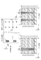
- FIG. 6 is a diagram showing a layout configuration of the memory cell array 18, and is a top view of the uppermost semiconductor layer 31, and the selection gate lines SGDL and SGSL. In the example of FIG. 6, a part of the insulating layer is omitted.
- the memory cell array 18 includes a memory cell area, an SGD area, an SGS area, a selected gate contact area corresponding to the selected gate line SGDL, and a selected gate contact area corresponding to the selected gate line SGSL.
- a memory cell transistor MC is provided in the memory cell area.
- the memory cell transistor MC includes a part of the semiconductor layer 31, a word line pillar WLP, a block insulating layer described later, a charge storage layer, and a tunnel insulating layer.
- the memory cell transistor MC may be simply described as a word line pillar WLP.
- the SGD area is provided adjacent to the memory cell area in the X direction, and functions as a connection area between the semiconductor layer 31 and the contact plug CBL.
- the selection transistor ST1 is provided in the SGD region.
- the SGS region is provided adjacent to the memory cell region in the X direction, and functions as a connection region between the semiconductor layer 31 and the contact plug CSL.
- the selection transistor ST2 is provided in the SGS region.
- the selection gate contact area corresponding to the selection gate line SGDL is provided adjacent to the SGD area in the X direction, and the contact plug CSGD and the selection gate line SGDL are connected.
- the selection gate contact area corresponding to the selection gate line SGSL is provided adjacent to the SGS area in the X direction, and the contact plug CSGS and the selection gate line SGSL are connected to each other.
- the number of memory cell areas, SGD areas, SGS areas, selected gate contact areas corresponding to the selected gate line SGDL, and selected gate contact areas corresponding to the selected gate line SGSL included in the memory cell array 18 is arbitrary.
- a plurality of (12 in the example of FIG. 6) semiconductor layers extending in the X direction (or row direction) are arranged along the Y direction (or column direction).
- Word line pillars WLPs are arranged between the semiconductor layers 31 in the Y direction in a staggered arrangement in the X and Y directions.
- the word line pillars WLP1 and WLP2 are arranged next to each other in the X direction
- the word line pillars WLP3 are arranged between the word line pillars WLP1 and WLP2 in the X direction
- the word line pillars WLP1 and WLP2 are arranged in the Y direction. It is placed in a different position from.
- a plurality of word line pillar WLPs (or memory cell transistors MC) (11 or 12 in the example of FIG. 6) are predetermined between the two semiconductor layers 31 along the X direction. It is arranged at the arrangement pitch P1 of.
- the plurality of word line pillars WLP adjacent to each other in the Y direction are also arranged along the X direction at a predetermined arrangement pitch P1 and are arranged so as to be offset by P1 / 2 in the X direction.
- a plurality of insulating pillars HR1 are arranged at a predetermined distance in the Y direction.
- the insulating pillar HR1 is arranged every other row with respect to the word line pillar WLP arranged in the X direction in the Y direction.
- the insulating pillar HR1 is arranged between two word line pillars WLP arranged in the X direction. In other words, in the word line pillar WLP arranged in the X direction and the Y direction, one row of the word line pillar WLP arranged in the Y direction is replaced with the insulating pillar HR1.
- one row (or a plurality of rows) of word line pillars WLP adjacent to each side in the X direction is a dummy word line pillar with respect to one row of insulating pillars HR1 arranged in the Y direction. It may be set to WDLP.
- the memory cell transistor provided in the dummy word line pillar WDLP is set to a dummy memory cell transistor (hereinafter, also referred to as a dummy cell).
- the number of dummy word line pillars DKLP (that is, dummy memory cell transistors) is arbitrary and may be 0.
- a selective gate SGD is provided on the side surface of the semiconductor layer 31 via a gate oxide layer.
- a plurality of (12 in the example of FIG. 6) contact plugs CBL are connected to a plurality of semiconductor layers 31 arranged along the Y direction.
- the plurality of contact plugs CBLs are provided in a staggered arrangement of four rows (rows) along the Y direction. That is, four contact plugs CBL adjacent to each other in the Y direction are arranged while repeating the four-row pattern in which the four contact plugs CBL are arranged while changing their positions in the X direction.
- the contact plugs CBL1 to CBL4 are arranged while shifting their positions in the X direction in order.
- the contact plug CBL2 adjacent to the contact plug CBL1 is provided at a position different from that of the contact plug CBL1 in the X direction.
- the contact plug CBL3 adjacent to the contact plug CBL2 is provided at a position different from that of the contact plugs CBL1 and CBL2 in the X direction.
- the contact plug CBL4 adjacent to the contact plug CBL3 is provided at a position different from that of the contact plugs CBL1, CBL2, and CBL3 in the X direction.
- the distance between the contact plugs CBL1 and CBL2, the distance between the contact plug CBL2 and the contact plug CBL3, and the distance between the contact plugs CBL3 and CBL4 in the X direction are substantially the same.
- the contact plugs CBL1 to CBL4 are arranged so as to be.
- Such a four-strand staggered arrangement is repeated in the Y direction.
- the contact plug CBL5 adjacent to the contact plug CBL4 in the Y direction is arranged at the same position as the contact plug CBL1 in the X direction.
- the positions of the contact plugs CBL1 to CBL4 in the X direction in the four staggered arrangement are arbitrary.
- the contact plugs CBL1 to CBL4 may not be arranged at the same interval in the X direction, and the order of the contact plugs CBL1 to CBL4 in the X direction may be changed.
- the arrangement of the contact plug CBL is not limited to the quadruple staggered arrangement.
- the plurality of contact plugs CBL may be arranged in a row along the Y direction, or may be arranged in a staggered arrangement of two or more.
- a selective gate SGS is provided on the side surface of the semiconductor layer 31 via a gate oxide layer.
- the two semiconductor layers 31 adjacent to each other along the Y direction are bundled into one and commonly connected to one contact plug CSL.
- two semiconductor layers 31 are commonly connected to one contact plug CSL, but the present invention is not limited to this.
- one contact plug CSL may be provided on one semiconductor layer 31, or three or more semiconductor layers 31 may be bundled and commonly connected to one contact plug CSL.
- a plurality of contact plug CSGDs are provided along the Y direction.
- the plurality of contact plugs CSGD penetrate the plurality of selective gate lines SGDL stacked in the Z direction and are electrically connected to any one of the plurality of selective gate lines SGDL.
- a plurality of insulating pillars HR2 penetrating the plurality of selection gate lines SGDL stacked in the Z direction are provided.
- the arrangement of the insulating pillar HR2 is arbitrary.
- the insulating pillar HR2 is formed by an insulating layer and is not electrically connected to other wiring.
- a plurality of contact plugs CSGS are provided along the Y direction.
- the plurality of contact plugs CSGS penetrate the plurality of selective gate wires SGSL stacked in the Z direction and are electrically connected to any one of the plurality of selective gate wires SGSL.
- a plurality of insulating pillars penetrating the plurality of selection gate lines SGSL stacked in the Z direction are similarly formed in the selection gate contact area corresponding to the selection gate line SGDL.
- HR2 is provided.
- the arrangement of the insulating pillar HR2 is arbitrary.
- the insulating pillar HR2 is formed by an insulating layer and is not electrically connected to other wiring.
- FIG. 7 is a cross-sectional view of the memory cell array 18 along the X direction. In FIG. 7, a part of the insulating layer is omitted.
- a memory cell array 18 is provided above the semiconductor substrate 50.
- the global selection gate lines GSGDL and GSGSL are provided above the semiconductor substrate 50.
- An insulating layer 52 is provided on the global selection gate lines GSGDL and GSGSL.
- a plurality of laminated semiconductor layers 31 are provided above the insulating layer 52.
- the semiconductor layer 31 in the memory cell region is provided with a contact plug CWL_1 (or a word line pillar WLP) so as to penetrate the semiconductor layer 31.
- a word line WL_1 is provided on the contact plug CWL_1.
- a contact plug CBL_1 is provided in the semiconductor layer 31 in the SGD region so as to penetrate the semiconductor layer 31.
- a contact plug CH_1 is provided on the contact plug CBL_1.
- a contact plug VY is provided on the contact plug CH_1. Further, a bit wire BL extending in the X direction is provided on the contact plug VY.
- a contact plug CSL_1 is provided in the semiconductor layer 31 in the SGS region so as to penetrate the semiconductor layer 31. Further, a source line SL_1 is provided on the contact plug CSL_1.
- the contact plug CSGD in the selected gate contact area is connected to any one of the selected gate lines SGDL, and the bottom surface of the contact plug CSGD is connected to the global selected gate line GSGDL.
- the contact plug CSGS is connected to any one of the selection gate lines SGSL, and the bottom surface of the contact plug CSGS is connected to the global selection gate line GSGSL.
- FIG. 8 is an enlarged view of the region RA in FIG. 7, and shows a layout configuration including the insulating pillar HR1 near the center in the memory cell region. In the example of FIG. 8, a part of the insulating layer is omitted.
- each of the plurality of semiconductor layers 31 extends in the X direction.
- the semiconductor layers 31 are arranged at a predetermined distance along the Y direction.
- the semiconductor layer 31 contains, for example, polysilicon to which impurities have been added.
- a memory trench MT is provided between the two semiconductor layers 31 arranged along the Y direction.
- the memory trench MT is a groove provided to separate the semiconductor layer 31 along the Y direction, and an insulating layer 55 is embedded in the memory trench MT.
- the insulating layer 55 contains, for example, silicon oxide (SiO 2 ).
- An insulating layer 32 is provided between the semiconductor layer 31 and the insulating layer 55.
- the insulating layer 32 functions as an etching stopper when forming the tunnel insulating layer 36 and the charge storage layer 35, which will be described later.
- the insulating layer 32 contains, for example, silicon nitride.
- the word line pillar WLP includes a conductive layer 33 (or contact plug CWL) extending in the Z direction and an insulating layer 34.
- the conductive layer 33 is electrically connected to the upper word line WL and functions as a control gate (or word line) of the memory cell transistor MC.
- a conductive material is used for the conductive layer 33.
- the conductive material may be a metal material, a metal compound, or a semiconductor material to which impurities have been added.
- the conductive layer 33 contains, for example, tungsten (W) and titanium nitride (TiN). TiN is used as a barrier metal when W is formed by CVD (chemical vapor deposition).
- the insulating layer 34 is provided on the side surface of the conductive layer 33 so as to surround the periphery of the conductive layer 33 in the X and Y directions.
- the insulating layer 34 functions as a block insulating layer that prevents the charges accumulated in the charge storage layer 35 from diffusing into the conductive layer 33 (ward wire).
- An insulating material is used for the insulating layer 34.
- the insulating material includes, for example, a high dielectric constant film such as an oxide or a nitride such as aluminum (Al), hafnium (Hf), titanium (Ti), zirconia (Zr) and lanthanum (La), or silicon oxide or silicon.
- a high pressure resistant film such as oxynitride, a mixture thereof, or a laminated film is used.
- a charge storage layer 35 and a tunnel insulating layer 36 are provided between the word line pillar WLP and the semiconductor layer 31 from the word line pillar WLP side. Specifically, the charge storage layer 35 is arranged between the insulating layer 34 and the semiconductor layer 31. Further, a tunnel insulating layer 36 is arranged between the charge storage layer 35 and the semiconductor layer 31.
- the charge storage layer 35 has a function of storing the charge injected from the semiconductor layer 31 in the memory cell transistor MC.
- the charge storage layer 35 may be, for example, an FG type using a conductive layer or a MONOS type using an insulating layer.
- the charge storage layer 35 may also include both an FG type using a conductive layer and a MONOS type using an insulating layer.
- the case where the charge storage layer 35 is of the FG type will be described.
- silicon is used, and metal nitrides such as silicon nitride, tantalum nitride (TaN) and titanium nitride (TiN), metallic silicon compounds such as tungsten (W) and ruthenium (Ru), and metals are used.
- metal nitrides such as silicon nitride, tantalum nitride (TaN) and titanium nitride (TiN), metallic silicon compounds such as tungsten (W) and ruthenium (Ru), and metals are used.
- a mixture such as silicon or an insulating film mixed with fine particles, a laminated film, or the like is used.
- the tunnel insulating layer 36 for example, a mixture of silicon oxide (SiO 2 ), silicon nitride (SiN) or silicon oxynitride (SiON), or a laminated film is used.
- a charge storage layer 35, a tunnel insulating layer 36, and a semiconductor layer 31 are provided at the first and second ends of the word line pillar WLP in the Y direction.
- the block insulating layer 34 is arranged so as to surround the conductive layer 33
- the first charge storage layer 35 is arranged at the first end of the block insulating layer 34 in the Y direction
- the first charge storage layer 35 is arranged at the first end of the block insulating layer 34 in the Y direction
- the first charge storage layer 35 is arranged on the side surface of the first tunnel insulating layer 36 in the Y direction
- the semiconductor layer 31 is arranged on the side surface of the first tunnel insulating layer 36 in the Y direction.
- the conductive layer 33, the block insulating layer 34, the first charge storage layer 35, the first tunnel insulating layer 36, and the semiconductor layer 31 constitute, for example, a memory cell transistor MCa.
- the second charge storage layer 35 is arranged at the second end of the block insulating layer 34 in the Y direction
- the second tunnel insulating layer 36 is arranged on the side surface of the second charge storage layer 35 in the Y direction
- the second is further.
- the semiconductor layer 31 is arranged on the side surface of the tunnel insulating layer 36 in the Y direction.
- the conductive layer 33, the block insulating layer 34, the second charge storage layer 35, the second tunnel insulating layer 36, and the semiconductor layer 31 constitute, for example, a memory cell transistor MCb.
- insulating layers 55 are arranged at both ends of the word line pillar WLP in the X direction.
- the plurality of insulating pillars HR1 are arranged between the two word line pillars WLP in the X direction and arranged in a row in the Y direction.
- a word line pillar WLP, an insulating pillar HR1, and a word line pillar WLP are sequentially arranged between the two semiconductor layers 31 along the X direction at a predetermined arrangement pitch.
- An insulating layer 55 (or a memory trench MT) is arranged between the word line pillar WLP and the insulating pillar HR1.
- the second word line pillar WLP is replaced with the insulating pillar HR1.
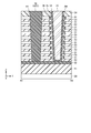
- FIG. 9 is a cross-sectional view taken along the line A1-A2 (or the Y direction) of the memory cell area in the memory cell array 18.
- FIG. 10 is a cross-sectional view taken along line B1-B2 (or the X direction) of the memory cell area in the memory cell array 18.
- the insulating layer 51 is provided on the semiconductor substrate 50.
- the insulating layer 51 may include, for example, a transistor (not shown) formed on the semiconductor substrate 50 or a plurality of wiring layers (not shown).
- the insulating layer 51 contains, for example, silicon oxide (SiO 2 ).
- a memory cell array 18 is provided on the insulating layer 51.
- the insulating layer 52 is provided on the insulating layer 51.
- the insulating layer 52 functions as an etching stopper when processing holes used in memory trench MTs, various contact plugs, and the like.
- the insulating layer 52 may be an insulating material capable of obtaining a sufficient etching selectivity with respect to the insulating layer 53 provided on the upper layer.
- the insulating layer 52 contains, for example, a metal oxide such as silicon nitride (SiN) or aluminum oxide (AlO).
- An insulating layer 53 is provided on the insulating layer 52.
- the insulating layer 53 contains, for example, silicon oxide.
- nine semiconductor layers 31 are laminated with the insulating layer 53 interposed therebetween. That is, nine insulating layers 53 and nine semiconductor layers 31 are alternately laminated on the insulating layer 52 to form a laminated body.
- the number of layers of the semiconductor layer 31 is arbitrary.
- An insulating layer 54 is provided on the uppermost semiconductor layer 31.
- the insulating layer 54 contains, for example, silicon oxide.
- the word wire pillar WLP extends in the Z direction so as to intersect with the insulating layer 54, the alternately laminated nine-layer semiconductor layer 31 and the nine-layer insulating layer 53 (that is, the laminated body).
- the word line pillar WLP is formed in the Z direction between the insulating layer 54, the semiconductor layer 31, and the insulating layer 53 and the insulating layer 54, the semiconductor layer 31, and the insulating layer 53 adjacent to each other in the Y direction from above the insulating layer 54. To reach the insulating layer 52.
- the word wire pillar WLP includes a conductive layer 33 and an insulating layer 34 extending in the Z direction.
- the hole AH is formed in the Z direction so as to intersect the insulating layer 54, the semiconductor layer 31, and the insulating layer 53.
- An insulating layer 34 is formed on the side surface and the bottom surface of the hole AH.
- a conductive layer 33 is formed on the side surface of the insulating layer 34 so as to embed the inside of the hole AH.
- a charge storage layer 35 and a tunnel insulating layer 36 are provided between the insulating layer 34 and the semiconductor layer 31 from the insulating layer 34 side. Specifically, a charge storage layer 35 is provided between the insulating layer 34 and the semiconductor layer 31 so as to come into contact with the side surface of the insulating layer 34. Further, a tunnel insulating layer 36 is provided between the charge storage layer 35 and the semiconductor layer 31.
- the insulating pillar HR1 extends in the Z direction so as to intersect the insulating layer 54, the alternately laminated nine-layer semiconductor layer 31 and the nine-layer insulating layer 53.
- the insulating pillar HR1 is formed in the Z direction between the insulating layer 54, the semiconductor layer 31, and the insulating layer 53 and the insulating layer 54, the semiconductor layer 31, and the insulating layer 53 adjacent to each other in the Y direction from above the insulating layer 54. As it passes, it reaches the insulating layer 52.
- the insulating pillar HR1 includes an insulating layer 56 extending in the Z direction. Specifically, the hole H1 is formed in the Z direction so as to intersect the insulating layer 54, the semiconductor layer 31, and the insulating layer 53. Further, the insulating layer 56 is formed so as to embed the inside of the hole H1.
- the memory trench MT is formed in the Z direction between the insulating layer 54, the semiconductor layer 31, and the insulating layer 53 and the insulating layer 54, the semiconductor layer 31, and the insulating layer 53 adjacent to each other in the Y direction from above the insulating layer 54. As it passes, it reaches the insulating layer 52. An insulating layer 55 is provided inside the memory trench MT. Further, an insulating layer 32 is provided between the insulating layer 55 and the semiconductor layer 31.
- 11 to 17 are views showing a method of manufacturing a part of the memory cell area and the selected gate contact area in the memory cell array 18.
- 11 to 17 show the upper surface (upper surface of the semiconductor layer) of the uppermost semiconductor layer 31 in the manufacturing process, the cross section along the A1-A2 line (A1-A2 cross section), and the cross section along the B1-B2 line (the cross section along the B1-B2 line). B1-B2 cross section) are shown respectively.
- the insulating layer 51 and the insulating layer 52 are sequentially laminated on the semiconductor substrate 50.
- nine insulating layers 53 and nine semiconductor layers 31 are alternately laminated on the insulating layer 52.
- the insulating layer 54 is formed on the uppermost semiconductor layer 31.
- insulating pillars HR1 and HR2 are formed in the memory cell area and the selected gate contact area using the same process, respectively. That is, the insulating pillar HR1 is formed in the memory cell region so as to penetrate the insulating layer 54, the insulating layer 53, and the semiconductor layer 31. Using this step for forming the insulating pillar HR1, the insulating pillar HR2 is formed in the selective gate contact region so as to penetrate the insulating layer 54, the insulating layer 53, and the semiconductor layer 31.
- the hole H1 for the insulating pillar HR1 that penetrates the insulating layer 54, the semiconductor layer 31 of the nine layers, and the insulating layer 53 of the nine layers and reaches the insulating layer 52 at the bottom surface is a memory cell area.
- the hole H2 for the insulating pillar HR2 is formed in the selective gate contact region.
- the insulating layer 56 contains, for example, silicon oxide.
- the insulating pillars HR1 and HR2 are formed in the memory cell region and the selective gate contact region by using the same process, but of course, one of the insulating pillars HR1 and the insulating pillars HR2 is formed first, and then the other is formed. You may.
- a memory trench MT is formed in the memory cell area. Specifically, for example, by dry etching, a memory trench MT is formed which penetrates the insulating layer 54, the semiconductor layer 31 of the nine layers, and the insulating layer 53 of the nine layers, and the bottom surface reaches the insulating layer 52.
- the insulating pillar HR1 is left as it is.
- a plurality of laminated semiconductor layers 31 are formed. These laminated semiconductor layers 31 have a high aspect ratio and are easily collapsed (or buckled). In the present embodiment, since the insulating pillar HR1 is arranged between the laminated semiconductor layers 31, it is possible to prevent such collapse of the semiconductor layers 31.
- a part of the semiconductor layer 31 is removed from the side surface in the memory trench MT, and the insulating layer 32 is formed in the removed region. Further, an insulating layer 55 is formed in the memory trench MT.
- a part of the semiconductor layer 31 is etched from the side surface of the opened memory trench MT to form a recess region.
- the insulating layer 32 is formed on the side surface and the bottom surface in the memory trench MT including the recess region and on the insulating layer 54.
- the side surface and the bottom surface in the memory trench MT and the excess insulating layer 32 on the insulating layer 54 are removed by etching back (or dry etching) to leave the insulating layer 32 in the recess region.
- CVD the inside of the memory trench MT is embedded with the insulating layer 55.
- a part of the insulating layer 55 is removed to form a hole AH in the region where the word line pillar WLP should be provided by, for example, dry etching.
- an insulating layer 36 and a charge storage layer 35 are formed on the side surface of the hole AH in the Y direction.
- the insulating layer 32 around the hole AH is removed by wet etching.
- the side surface of the semiconductor layer 31 exposed from the hole AH is oxidized by the oxidation treatment to form the insulating layer 36.
- the charge storage layer 35 is formed on the side surface and the bottom surface in the hole AH and on the insulating layer 54. Further, the side surface and the bottom surface in the hole AH and the excess charge storage layer 35 on the insulating layer 54 are removed by etchback, leaving the charge storage layer 35 on the side surface of the insulating layer 36.
- the insulating layer 34 is formed on the bottom surface and the side surface in the hole AH, and then the conductive layer 33 is formed inside the hole AH.
- the insulating layer 34 is formed on the bottom surface and the side surface in the hole AH by CVD.
- CVD for example, TiN and W as the conductive layer 33 are sequentially formed.
- TiN and W on the insulating layer 54 are removed by, for example, CMP (chemical mechanical polishing).
- one row of insulating pillars HR1 arranged in the Y direction is provided in the memory cell area. Insulation pillars HR1 arranged in the Y direction may be provided in a plurality of rows.
- FIG. 18 is a diagram showing a layout configuration of a semiconductor storage device of a modified example.
- insulating pillars HR1-1 arranged in the Y direction are provided in the memory cell area at a distance D2 from the contact plug CSGD (or contact plug CBL5). Further, the insulating pillar HR1-2 is provided at a distance D2 from the insulating pillar HR1-1.
- the distance D2 is also set between the insulating pillar HR1-2 and the contact plug CSGSD (or contact plug CSL). That is, the distances D2 between the insulating pillar HR1_1 and the contact plug CSGD, between the insulating pillar HR1-1 and the insulating pillar HR1-2, and between the insulating pillar HR1-2 and the contact plug CSGS are set to be substantially equal.
- one row of the word line pillar WLP arranged in the Y direction is replaced with the insulated pillar HR1-1 and the insulated pillar HR_2, respectively.
- the semiconductor storage device has, for example, a laminate in which a plurality of semiconductor layers 31 and a plurality of insulating layers 53 are laminated in the Z direction.
- a memory trench MT is formed in a laminated body in a manufacturing process of a semiconductor storage device, the laminated body is separated by the memory trench MT to become a laminated body having a high aspect ratio, and the laminated body collapses (or buckles) due to stress. In some cases.
- the insulating pillar HR1 extending in the Z direction is provided in the laminated body in which the plurality of semiconductor layers 31 and the plurality of insulating layers 53 in the memory cell region are laminated.
- the insulating pillars HR1 are arranged near the center of the memory cell region in the X direction at a predetermined distance in the Y direction.
- the distance between the insulating pillar HR1 and the contact plug CSGD (or the contact plug CBL) and the distance between the insulating pillar HR1 and the contact plug CSGS (or the contact plug CSL) are set to approximately equal distance D1.
- one word line pillar WLP is replaced with an insulating pillar HR1.
- the insulating pillars HR1-1 and HR1-2 extending in the Z direction are provided in the laminated body in which the plurality of semiconductor layers 31 and the plurality of insulating layers 53 in the memory cell region are laminated.
- the distance D2 between the insulating pillar HR1-1 and the contact plug CSGD, between the insulating pillar HR1-1 and the insulating pillar HR1-2, and between the insulating pillar HR1-2 and the contact plug CSGS is set to be approximately the same.
- the insulating pillars HR1 or the insulating pillars HR1-1 and HR1-2 support the laminated body, and the laminated body in the memory cell area is prevented from collapsing (or buckling). be able to.
- the insulating pillar HR1 in the memory cell region by using the same process as the manufacturing process of the insulating pillar HR2 provided in the selective gate contact region, it is possible to prevent an increase in the number of manufacturing steps, and the manufacturing process. The increase in strike can be suppressed.
- the semiconductor storage device of the second embodiment will be described.
- the second embodiment instead of replacing the word line pillar WLP with the insulating pillar HR1 as in the first embodiment, an example in which the insulated pillar HR1 is provided between two word line pillar WLPs arranged at a predetermined arrangement pitch. Is shown.
- Other circuit configurations, overall configurations, layout configurations, and cross-sectional structures are the same as those in the first embodiment described above.
- the second embodiment mainly describes the differences from the first embodiment.
- FIG. 19 is a diagram showing a layout configuration of the memory cell array 18, and is a top view of the uppermost semiconductor layer 31, and the selection gate lines SGDL and SGSL. In the example of FIG. 19, a part of the insulating layer is omitted.
- the layout configuration of the memory cell array 18 is the same as the configuration shown in FIG. 6 of the first embodiment except for the configuration of the memory cell area.
- FIG. 20 is an enlarged view of the region RA in FIG. 19, and shows a layout configuration including the insulating pillar HR1 near the center in the memory cell region. In the example of FIG. 20, a part of the insulating layer is omitted.
- word line pillar WLPs (or memory cell transistors MC) are arranged along the X direction (or row direction) at a predetermined array pitch P1.
- a plurality of insulating pillars HR1 are arranged at a predetermined distance in the Y direction near the center of the memory cell area in the X direction.
- the insulating pillar HR1 is arranged every other row with respect to the WLP arranged in the X direction in the Y direction.
- the insulating pillar HR1 is arranged between two word line pillar WLPs arranged in the X direction at an arrangement pitch P1. Further, the insulating pillar HR1 is in contact with these two word line pillar WLPs sandwiching the insulating pillar HR1. Further, an insulating layer 55 is arranged between the word line pillars WLP on which the insulating pillar HR1 is not arranged.
- the semiconductor storage device of the modification of the second embodiment will be described.
- the insulating pillar HR1 is provided between two adjacent word line pillar WLPs so as to be in contact with the word line pillar WLPs.
- the insulating pillar HR1 is provided between two adjacent word line pillar WLPs so as not to come into contact with these word line pillar WLPs.
- an insulating pillar HR1 is provided in the vicinity of the SGD area of the memory cell area.
- FIG. 21 is a diagram showing a layout configuration of a semiconductor storage device of a modified example.
- a plurality of (6 or 7 in the example of FIG. 21) word line pillar WLPs are X. They are arranged at a predetermined array pitch P2 along the direction (or row direction). Similarly, the plurality of word line pillars WLPs adjacent to each other in the Y direction are also arranged at a predetermined arrangement pitch P2 along the X direction and are arranged so as to be offset by P2 / 2 in the X direction.
- a plurality of insulating pillars HR1-1 are arranged in the Y direction at a predetermined distance near the center of the memory cell area in the X direction.
- the insulating pillars HR1-1 are arranged every other row with respect to the word line pillars WLP arranged in the X direction in the Y direction. That is, the plurality of insulating pillars HR1-11 are arranged in a row in the Y direction with the word line pillar WLP interposed between the insulating pillars HR1-1 adjacent to each other in the Y direction.
- the insulating pillar HR1-1 is arranged between two word line pillars WLP arranged at an arrangement pitch P2 in the X direction.
- the insulating pillar HR1-1 is not in contact with the two word line pillar WLPs sandwiching the insulating pillar HR1-1.
- a plurality of insulating pillars HR1-2 are arranged at a predetermined distance in the Y direction.
- the plurality of insulating pillars HR1-2 are arranged at one end of the memory cell area in the X direction.
- the insulating pillar HR1-2 is not in contact with the adjacent word line pillar WLP.
- the insulating pillars HR1-1 arranged in the Y direction are provided at a distance of D3 from the contact plug CSGS (or contact plug CSL).
- the insulating pillars HR1-2 arranged in the Y direction are provided at a distance D3 from the insulating pillars HR1-1. That is, the distance D3 between the insulating pillar HR1-1 and the contact plug CSGS and between the insulating pillar HR1-1 and the insulating pillar HR1-2 are set to be substantially equal.
- the insulating pillar HR1_1 is for preventing the collapse of the memory cell area
- the insulating pillar HR1-2 is for preventing the collapse of the SGD area.
- one row (or a plurality of rows) of word line pillars WLP adjacent to the X direction is set as the dummy word line pillar WDLP with respect to the one row of insulated pillars HR1-2 arranged in the Y direction. May be done.
- the memory cell transistor provided in the dummy word line pillar WDLP is set to the dummy memory cell transistor.
- the number of dummy word line pillars DKLP (that is, dummy memory cell transistors) is arbitrary and may be 0.
- the insulating pillar HR1 extending in the Z direction is provided in the laminated body in which the plurality of semiconductor layers 31 and the plurality of insulating layers 53 in the memory cell region are laminated.
- the insulating pillars HR1 are arranged near the center of the memory cell region in the X direction at a predetermined distance in the Y direction.
- the distance between the insulating pillar HR1 and the contact plug CSGD (or the contact plug CBL) and the distance between the insulating pillar HR1 and the contact plug CSGS (or the contact plug CSL) are set to approximately equal distance D1.
- the insulating pillar HR1 is arranged between two adjacent word line pillar WLPs in a plurality of word line pillar WLPs arranged in the X direction at an array pitch P1 so as to be in contact with the two word line pillar WLPs. ing.
- the insulating pillars HR1-1 and HR1-2 extending in the Z direction are provided in the laminated body in which the plurality of semiconductor layers 31 and the plurality of insulating layers 53 in the memory cell region are laminated.
- the insulating pillars HR1-1 are arranged near the center of the memory cell area in the X direction at a predetermined distance in the Y direction.
- the insulating pillar HR1-1 is arranged between two adjacent word line pillar WLPs in a plurality of word line pillar WLPs arranged in the X direction at an array pitch P2 so as not to contact the two word line pillar WLPs. ..
- the insulating pillars HR1-2 are arranged between the memory cell area and the SGD area at a predetermined distance in the Y direction.
- the distance D3 between the insulating pillar HR1_1 and the contact plug CSGS and between the insulating pillar HR1-1 and the insulating pillar HR1-2 are set to be substantially equal.
- the insulating pillars HR1 and HR1-11 support the laminated body, and the laminated body in the memory cell region can be prevented from collapsing (or buckling). Further, in the modified example, the insulating pillar HR1-2 supports the laminated body, and it is possible to prevent the laminated body in the SGD region from collapsing.
- the insulated pillars HR1 or the insulated pillars HR1-1 and HR1-2 are arranged between two adjacent word line pillars WLPs, so that the memory in the memory cell area is stored. It does not reduce the occupancy of the cell transistor MC.
- the insulating pillars HR1 or the insulating pillars HR1-1 and HR1-2 in the memory cell region by using the same process as the manufacturing process of the insulating pillar HR2 provided in the selection gate contact region. , It is possible to prevent an increase in the number of manufacturing processes and suppress an increase in manufacturing work strikes.
- the NAND flash memory has been described as an example as the semiconductor storage device, but the present invention is not limited to the NAND flash memory, and can be applied to other semiconductor memories in general, and various types other than the semiconductor memory. Applicable to storage devices.
Landscapes
- Semiconductor Memories (AREA)
- Non-Volatile Memory (AREA)
Abstract
Dispositif de stockage à semi-conducteur qui, selon les modes de réalisation, comprend une première couche semi-conductrice qui s'étend dans une première direction, une seconde couche semi-conductrice qui s'étend dans la première direction et est placée de façon à être séparée de la première couche semi-conductrice dans une seconde direction qui croise la première direction, une première couche de conduction qui s'étend dans la seconde direction et coupe la première couche semi-conductrice et la seconde couche semi-conductrice, une première couche d'isolation qui s'étend dans la seconde direction, coupe la première couche semi-conductrice et la seconde couche semi-conductrice, et est placée à une première distance de la première couche de conduction dans la première direction, une deuxième couche de conduction qui s'étend dans la seconde direction, coupe la première couche semi-conductrice et la seconde couche semi-conductrice, et est placée à la première distance de la première couche d'isolation dans la première direction, et une troisième couche de conduction qui s'étend dans la seconde direction, coupe la première couche semi-conductrice et la deuxième couche semi-conductrice, et est placée à la première distance de la deuxième couche de conduction dans la première direction.
Priority Applications (3)
| Application Number | Priority Date | Filing Date | Title |
|---|---|---|---|
| PCT/JP2020/013071 WO2021192051A1 (fr) | 2020-03-24 | 2020-03-24 | Dispositif de stockage à semi-conducteur |
| CN202080098046.5A CN115210871A (zh) | 2020-03-24 | 2020-03-24 | 半导体存储装置 |
| US17/944,063 US20230014439A1 (en) | 2020-03-24 | 2022-09-13 | Semiconductor memory device |
Applications Claiming Priority (1)
| Application Number | Priority Date | Filing Date | Title |
|---|---|---|---|
| PCT/JP2020/013071 WO2021192051A1 (fr) | 2020-03-24 | 2020-03-24 | Dispositif de stockage à semi-conducteur |
Related Child Applications (1)
| Application Number | Title | Priority Date | Filing Date |
|---|---|---|---|
| US17/944,063 Continuation US20230014439A1 (en) | 2020-03-24 | 2022-09-13 | Semiconductor memory device |
Publications (1)
| Publication Number | Publication Date |
|---|---|
| WO2021192051A1 true WO2021192051A1 (fr) | 2021-09-30 |
Family
ID=77891185
Family Applications (1)
| Application Number | Title | Priority Date | Filing Date |
|---|---|---|---|
| PCT/JP2020/013071 Ceased WO2021192051A1 (fr) | 2020-03-24 | 2020-03-24 | Dispositif de stockage à semi-conducteur |
Country Status (3)
| Country | Link |
|---|---|
| US (1) | US20230014439A1 (fr) |
| CN (1) | CN115210871A (fr) |
| WO (1) | WO2021192051A1 (fr) |
Cited By (2)
| Publication number | Priority date | Publication date | Assignee | Title |
|---|---|---|---|---|
| WO2023112236A1 (fr) * | 2021-12-16 | 2023-06-22 | キオクシア株式会社 | Dispositif de mémoire à semi-conducteurs |
| WO2024209331A1 (fr) * | 2023-04-07 | 2024-10-10 | 株式会社半導体エネルギー研究所 | Appareil de stockage et dispositif électronique |
Citations (4)
| Publication number | Priority date | Publication date | Assignee | Title |
|---|---|---|---|---|
| JP2011527515A (ja) * | 2008-07-10 | 2011-10-27 | コミッサリア ア レネルジー アトミーク エ オ ゼネルジ ザルタナテイヴ | マイクロ電子3dnandフラッシュメモリデバイスの構造および製造プロセス |
| JP2015228484A (ja) * | 2014-05-21 | 2015-12-17 | マクロニクス インターナショナル カンパニー リミテッド | 3d独立二重ゲートフラッシュメモリ |
| JP2016062624A (ja) * | 2014-09-17 | 2016-04-25 | 株式会社東芝 | 半導体記憶装置 |
| JP2016100596A (ja) * | 2014-11-19 | 2016-05-30 | マクロニクス インターナショナル カンパニー リミテッド | 垂直3dメモリデバイス、並びにその製造方法 |
Family Cites Families (7)
| Publication number | Priority date | Publication date | Assignee | Title |
|---|---|---|---|---|
| JP2008277543A (ja) * | 2007-04-27 | 2008-11-13 | Toshiba Corp | 不揮発性半導体記憶装置 |
| JP5193796B2 (ja) * | 2008-10-21 | 2013-05-08 | 株式会社東芝 | 3次元積層型不揮発性半導体メモリ |
| JP2014027181A (ja) * | 2012-07-27 | 2014-02-06 | Toshiba Corp | 半導体装置及びその製造方法 |
| US9397110B2 (en) * | 2014-05-21 | 2016-07-19 | Macronix International Co., Ltd. | 3D independent double gate flash memory |
| JP6948892B2 (ja) * | 2017-09-19 | 2021-10-13 | キオクシア株式会社 | 半導体記憶装置 |
| TWI691050B (zh) * | 2018-07-31 | 2020-04-11 | 日商東芝記憶體股份有限公司 | 半導體記憶裝置 |
| JP2020092141A (ja) * | 2018-12-04 | 2020-06-11 | キオクシア株式会社 | 半導体記憶装置 |
-
2020
- 2020-03-24 WO PCT/JP2020/013071 patent/WO2021192051A1/fr not_active Ceased
- 2020-03-24 CN CN202080098046.5A patent/CN115210871A/zh active Pending
-
2022
- 2022-09-13 US US17/944,063 patent/US20230014439A1/en active Pending
Patent Citations (4)
| Publication number | Priority date | Publication date | Assignee | Title |
|---|---|---|---|---|
| JP2011527515A (ja) * | 2008-07-10 | 2011-10-27 | コミッサリア ア レネルジー アトミーク エ オ ゼネルジ ザルタナテイヴ | マイクロ電子3dnandフラッシュメモリデバイスの構造および製造プロセス |
| JP2015228484A (ja) * | 2014-05-21 | 2015-12-17 | マクロニクス インターナショナル カンパニー リミテッド | 3d独立二重ゲートフラッシュメモリ |
| JP2016062624A (ja) * | 2014-09-17 | 2016-04-25 | 株式会社東芝 | 半導体記憶装置 |
| JP2016100596A (ja) * | 2014-11-19 | 2016-05-30 | マクロニクス インターナショナル カンパニー リミテッド | 垂直3dメモリデバイス、並びにその製造方法 |
Cited By (2)
| Publication number | Priority date | Publication date | Assignee | Title |
|---|---|---|---|---|
| WO2023112236A1 (fr) * | 2021-12-16 | 2023-06-22 | キオクシア株式会社 | Dispositif de mémoire à semi-conducteurs |
| WO2024209331A1 (fr) * | 2023-04-07 | 2024-10-10 | 株式会社半導体エネルギー研究所 | Appareil de stockage et dispositif électronique |
Also Published As
| Publication number | Publication date |
|---|---|
| CN115210871A (zh) | 2022-10-18 |
| US20230014439A1 (en) | 2023-01-19 |
Similar Documents
| Publication | Publication Date | Title |
|---|---|---|
| TWI819090B (zh) | 半導體記憶裝置 | |
| US11605646B2 (en) | Semiconductor storage device and method of manufacturing the same | |
| TWI728875B (zh) | 半導體記憶裝置 | |
| CN110416220B (zh) | 半导体存储装置 | |
| CN110943088B (zh) | 半导体存储装置及其制造方法 | |
| TWI780515B (zh) | 半導體記憶裝置 | |
| TWI714210B (zh) | 半導體記憶裝置 | |
| JP2020107673A (ja) | 半導体記憶装置 | |
| TWI777089B (zh) | 半導體記憶裝置 | |
| JP2019153626A (ja) | 半導体記憶装置 | |
| TWI768450B (zh) | 半導體記憶裝置 | |
| US20200185403A1 (en) | Semiconductor memory device | |
| JP2021034650A (ja) | 半導体記憶装置 | |
| US20230014439A1 (en) | Semiconductor memory device | |
| US20210313335A1 (en) | Memory device | |
| US20240099001A1 (en) | Semiconductor memory device and manufacturing method | |
| JP2021034649A (ja) | 半導体記憶装置 | |
| US11973024B2 (en) | Semiconductor memory device | |
| US10910059B2 (en) | Nonvolatile semiconductor memory device | |
| JP2025142809A (ja) | 半導体記憶装置および半導体記憶装置の製造方法 | |
| JP2025143059A (ja) | 半導体記憶装置 | |
| JP2023044255A (ja) | 半導体記憶装置およびその製造方法 |
Legal Events
| Date | Code | Title | Description |
|---|---|---|---|
| 121 | Ep: the epo has been informed by wipo that ep was designated in this application |
Ref document number: 20927812 Country of ref document: EP Kind code of ref document: A1 |
|
| NENP | Non-entry into the national phase |
Ref country code: DE |
|
| 122 | Ep: pct application non-entry in european phase |
Ref document number: 20927812 Country of ref document: EP Kind code of ref document: A1 |
|
| NENP | Non-entry into the national phase |
Ref country code: JP |