WO2021192176A1 - Dispositif de capture d'image - Google Patents
Dispositif de capture d'image Download PDFInfo
- Publication number
- WO2021192176A1 WO2021192176A1 PCT/JP2020/013789 JP2020013789W WO2021192176A1 WO 2021192176 A1 WO2021192176 A1 WO 2021192176A1 JP 2020013789 W JP2020013789 W JP 2020013789W WO 2021192176 A1 WO2021192176 A1 WO 2021192176A1
- Authority
- WO
- WIPO (PCT)
- Prior art keywords
- pixel
- read
- image
- signal
- circuit
- Prior art date
- Legal status (The legal status is an assumption and is not a legal conclusion. Google has not performed a legal analysis and makes no representation as to the accuracy of the status listed.)
- Ceased
Links
Images




Classifications
-
- G—PHYSICS
- G02—OPTICS
- G02B—OPTICAL ELEMENTS, SYSTEMS OR APPARATUS
- G02B7/00—Mountings, adjusting means, or light-tight connections, for optical elements
- G02B7/28—Systems for automatic generation of focusing signals
- G02B7/34—Systems for automatic generation of focusing signals using different areas in a pupil plane
-
- G—PHYSICS
- G03—PHOTOGRAPHY; CINEMATOGRAPHY; ANALOGOUS TECHNIQUES USING WAVES OTHER THAN OPTICAL WAVES; ELECTROGRAPHY; HOLOGRAPHY
- G03B—APPARATUS OR ARRANGEMENTS FOR TAKING PHOTOGRAPHS OR FOR PROJECTING OR VIEWING THEM; APPARATUS OR ARRANGEMENTS EMPLOYING ANALOGOUS TECHNIQUES USING WAVES OTHER THAN OPTICAL WAVES; ACCESSORIES THEREFOR
- G03B13/00—Viewfinders; Focusing aids for cameras; Means for focusing for cameras; Autofocus systems for cameras
- G03B13/32—Means for focusing
- G03B13/34—Power focusing
- G03B13/36—Autofocus systems
-
- H—ELECTRICITY
- H04—ELECTRIC COMMUNICATION TECHNIQUE
- H04N—PICTORIAL COMMUNICATION, e.g. TELEVISION
- H04N23/00—Cameras or camera modules comprising electronic image sensors; Control thereof
- H04N23/60—Control of cameras or camera modules
-
- H—ELECTRICITY
- H04—ELECTRIC COMMUNICATION TECHNIQUE
- H04N—PICTORIAL COMMUNICATION, e.g. TELEVISION
- H04N25/00—Circuitry of solid-state image sensors [SSIS]; Control thereof
- H04N25/40—Extracting pixel data from image sensors by controlling scanning circuits, e.g. by modifying the number of pixels sampled or to be sampled
- H04N25/42—Extracting pixel data from image sensors by controlling scanning circuits, e.g. by modifying the number of pixels sampled or to be sampled by switching between different modes of operation using different resolutions or aspect ratios, e.g. switching between interlaced and non-interlaced mode
-
- H—ELECTRICITY
- H04—ELECTRIC COMMUNICATION TECHNIQUE
- H04N—PICTORIAL COMMUNICATION, e.g. TELEVISION
- H04N25/00—Circuitry of solid-state image sensors [SSIS]; Control thereof
- H04N25/40—Extracting pixel data from image sensors by controlling scanning circuits, e.g. by modifying the number of pixels sampled or to be sampled
- H04N25/44—Extracting pixel data from image sensors by controlling scanning circuits, e.g. by modifying the number of pixels sampled or to be sampled by partially reading an SSIS array
- H04N25/445—Extracting pixel data from image sensors by controlling scanning circuits, e.g. by modifying the number of pixels sampled or to be sampled by partially reading an SSIS array by skipping some contiguous pixels within the read portion of the array
-
- H—ELECTRICITY
- H04—ELECTRIC COMMUNICATION TECHNIQUE
- H04N—PICTORIAL COMMUNICATION, e.g. TELEVISION
- H04N25/00—Circuitry of solid-state image sensors [SSIS]; Control thereof
- H04N25/40—Extracting pixel data from image sensors by controlling scanning circuits, e.g. by modifying the number of pixels sampled or to be sampled
- H04N25/46—Extracting pixel data from image sensors by controlling scanning circuits, e.g. by modifying the number of pixels sampled or to be sampled by combining or binning pixels
-
- H—ELECTRICITY
- H04—ELECTRIC COMMUNICATION TECHNIQUE
- H04N—PICTORIAL COMMUNICATION, e.g. TELEVISION
- H04N25/00—Circuitry of solid-state image sensors [SSIS]; Control thereof
- H04N25/60—Noise processing, e.g. detecting, correcting, reducing or removing noise
- H04N25/63—Noise processing, e.g. detecting, correcting, reducing or removing noise applied to dark current
- H04N25/633—Noise processing, e.g. detecting, correcting, reducing or removing noise applied to dark current by using optical black pixels
-
- H—ELECTRICITY
- H04—ELECTRIC COMMUNICATION TECHNIQUE
- H04N—PICTORIAL COMMUNICATION, e.g. TELEVISION
- H04N25/00—Circuitry of solid-state image sensors [SSIS]; Control thereof
- H04N25/60—Noise processing, e.g. detecting, correcting, reducing or removing noise
- H04N25/67—Noise processing, e.g. detecting, correcting, reducing or removing noise applied to fixed-pattern noise, e.g. non-uniformity of response
-
- H—ELECTRICITY
- H04—ELECTRIC COMMUNICATION TECHNIQUE
- H04N—PICTORIAL COMMUNICATION, e.g. TELEVISION
- H04N25/00—Circuitry of solid-state image sensors [SSIS]; Control thereof
- H04N25/70—SSIS architectures; Circuits associated therewith
- H04N25/703—SSIS architectures incorporating pixels for producing signals other than image signals
- H04N25/704—Pixels specially adapted for focusing, e.g. phase difference pixel sets
-
- H—ELECTRICITY
- H10—SEMICONDUCTOR DEVICES; ELECTRIC SOLID-STATE DEVICES NOT OTHERWISE PROVIDED FOR
- H10F—INORGANIC SEMICONDUCTOR DEVICES SENSITIVE TO INFRARED RADIATION, LIGHT, ELECTROMAGNETIC RADIATION OF SHORTER WAVELENGTH OR CORPUSCULAR RADIATION
- H10F39/00—Integrated devices, or assemblies of multiple devices, comprising at least one element covered by group H10F30/00, e.g. radiation detectors comprising photodiode arrays
- H10F39/80—Constructional details of image sensors
- H10F39/805—Coatings
- H10F39/8053—Colour filters
Definitions
- the present invention relates to an imaging device including an image sensor in which pixels are divided into a plurality of pixels.
- imaging devices such as digital cameras equipped with an image plane phase difference image sensor and performing image plane phase difference AF have become widespread.
- the image plane phase difference AF focuses from the current focus position without searching for the peak of the contrast value. Since the drive direction and the required drive amount of the focus lens for the purpose can be acquired, there is a feature that the focus can be adjusted at high speed.
- the pupil-divided light beam is photoelectrically converted by a photoelectric conversion element (an example of the photoelectric conversion element is a photodiode (PD), which is hereinafter referred to as PD for simplicity). It enables phase difference detection.
- a photoelectric conversion element an example of the photoelectric conversion element is a photodiode (PD), which is hereinafter referred to as PD for simplicity.
- PD photodiode
- the light-shielding image plane phase difference image sensor has a light-shielding structure that blocks a part of the light rays incident on the PD arranged under the microlens in the pixel, and the light rays incident from the photographing lens are captured by the pupil according to the arrangement of the light-shielding structure. It is a division method.
- the PD division type image plane phase difference image sensor is a method in which the light rays incident from the photographing lens are divided into pupils by dividing the PD in the pixel instead of having a light-shielding structure.
- the pupil division method in the PD division method is performed by changing the PD division method.
- pixel data for left pupil division is generated by adding and averaging a part of the 9-divided PD signal, and the other part is added and averaged.
- the pair for detecting the phase difference (for example, left and right pair, upper and lower pair, etc.) can be configured within one pixel, whereas in the light-shielding image plane phase difference image sensor, within one pixel. Since it cannot be configured and requires a plurality of pixels, the former can significantly improve the focus detection accuracy as compared with the latter.
- the number of PDs does not change in the light-shielding image plane phase difference image sensor as compared with the non-image plane phase difference image sensor, but the PD division type image plane phase difference image sensor corresponds to the number of pixel divisions n.
- the number of PDs increases n times.
- the PD division type image plane phase difference image sensor has n times the signal reading time as compared with the light-shielding type image plane phase difference image sensor (and the non-image plane phase difference image sensor), and the imaging rate and the imaging rate and the image sensor are increased.
- the acquisition rate of the phase difference information becomes 1 / n.
- the present invention has been made in view of the above circumstances, and provides an imaging device including an image sensor in which pixels are divided into a plurality of pixels, which can acquire phase difference information while suppressing a decrease in imaging rate. I am aiming.
- the imaging device when a plurality of pixels are arranged in a row direction and a direction in which the row direction intersects, and n is an integer of 2 or more, the plurality of pixels are each one microlens.
- An image that includes n photoelectric conversion elements and outputs an imaging signal related to n divided pixel signals generated by photoelectric conversion of light from the microlens by the n photoelectric conversion elements.
- the image sensor includes a sensor and an image processing circuit for image processing the imaging signal output from the image sensor, and the image sensor has the n for each pixel row composed of a plurality of pixels arranged in the row direction.
- the image pickup signal related to the divided pixel signals can be read out in the first read mode or the second read mode, and the first read mode is one by adding the n divided pixel signals.
- the second read mode n signals are generated from the n divided pixel signals and one pixel row is read in n rows.
- the image processing circuit processes the pixel signals of the pixel rows read in the first read mode and the n signals of the pixel rows read in the second read mode. , Generates image data in which pixel data is arranged in a predetermined order for each pixel row.
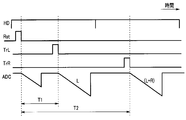
- the timing chart which shows the operation of the reading circuit of 1PD region in the image sensor of the said embodiment.
- the timing chart which shows the operation in the normal reading method of the reading circuit of the 2PD region in the image sensor of the said embodiment.
- the timing chart which shows the operation in the addition reading method of the reading circuit of the 2PD area in the image sensor of the said embodiment.
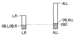
- the divided pixel signal read from the 2PD area and the pixel signal read from the 1PD area when the image sensor operates in the normal reading method and the image sensor has one OB clamp circuit.
- the pixel signal (L + R) read from the 2PD area and the pixel signal ALL read from the 1PD area of the image sensor operating in the additive reading method are OB clamped by one OB clamp circuit.
- the pixel signal (L + R) read from the 2PD area and the pixel signal ALL read from the 1PD area of the image sensor operating in the additive reading method are OB due to the difference in the CDS period.
- FIG. 1 to 15 show an embodiment of the present invention
- FIG. 1 is a block diagram showing a configuration of an image pickup apparatus.
- FIG. 1 shows an example in which the image pickup device is configured as, for example, a digital camera
- the image pickup device is not limited to the digital camera, and the digital video camera, the telephone device with a shooting function, the electronic endoscope, and the like.
- Any of various devices having an imaging function such as a microscope with an imaging function and a telescope with an imaging function, may be used.
- this image pickup apparatus includes a lens 1, an image sensor 2, an image processing circuit 3, a display 4, a camera shake sensor 6, a camera shake correction mechanism 7, a focus control mechanism 8, and the like. It includes a camera operating device 9 and a camera controller 10.
- the recording memory 5 is also shown in FIG. 1, the recording memory 5 may be configured to be detachable from the imaging device, and therefore is not unique to the imaging device. May be good.
- the lens 1 is an imaging optical system that forms an optical image of a subject on an image sensor 2.
- the lens 1 includes one or more lenses including a focus lens for adjusting the focus position (focus position) for focusing, and an aperture for controlling the range of the passing luminous flux.
- the camera shake correction function is also provided.
- a mechanical shutter for controlling the exposure time is further provided between the lens 1 and the image sensor 2.
- the image sensor 2 is arranged on the optical path of the photographing optical axis of the lens 1, and photoelectrically converts the optical image of the subject imaged by the lens 1 and outputs it as an imaging signal which is an electric signal.
- the image sensor 2 is arranged in a row direction and a direction in which a plurality of pixels intersect in the row direction.
- An example of the direction intersecting the row direction is a direction orthogonal to the row direction (column direction), but the direction is not limited to this, and the direction diagonally intersects the row direction (for example, arrangement of a so-called honeycomb structure). ) Etc. may be used.
- the plurality of pixels provided in the image sensor 2 are each a microlens ML (see FIG. 3), n photoelectric conversion elements PD (see FIG. 3), and n. It has. It should be noted that a general optical lens is usually composed of a plurality of lenses along the optical axis direction. Therefore, even in the case of a microlens ML composed of a plurality of lenses along the optical axis direction, it is counted as one microlens ML.
- the image sensor 2 outputs an imaging signal related to n divided pixel signals generated by photoelectric conversion of light from the microlens ML by n photoelectric conversion elements PD.
- the imaging signal related to the n divided pixel signals for example, when one pixel is divided into L (left) and R (right), the n divided pixel signals themselves (divided pixels).
- Signal L and divided pixel signal R signals that can configure n divided pixel signals (pixel signal (L + R) and divided pixel signal L) (or pixel signal (L + R) and divided pixel signal R) n divisions
- pixel signal (L + R) from 2PD region
- pixel signal ALL from 1PD region
- the image sensor 2 is a color image sensor in which color filters of a plurality of filter colors are arranged as repetitions of a predetermined basic arrangement so that one filter color corresponds to one microlens ML.
- the image sensor 2 is not limited to the color image sensor, and may be a monochrome image sensor.
- the predetermined basic array of the image sensor 2 is, for example, a Bayer array of 2 ⁇ 2 pixels (primary color Bayer array, complementary color Bayer array, etc.), but the present invention is not limited to this, and a basic array of 6 ⁇ 6 pixels may be used. I do not care. In the present embodiment, the case where the predetermined basic arrangement is the primary color Bayer arrangement will be described.
- the image sensor 2 is a so-called PD division type image plane phase difference image sensor in which the pixels are divided into a plurality of divided pixels.
- FIG. 3 is a chart showing an example of a 2-division and 4-division pixel division configuration and a read circuit in the image sensor 2.
- the primary color Bayer array is a basic array of 2 vertical x 2 horizontal pixels, and the basic array is periodically repeated in the row direction and the column direction.
- the green filters Gr and Gb are arranged diagonally, the red filter Rr is arranged in the same row as the green filter Gr, and the blue filter Bb is arranged in the same row as the green filter Gb. be.
- the green filter Gr and the green filter Gb have the same spectral characteristics, but they are distinguished according to which of the red filter Rr and the blue filter Bb has the same line.
- the filter color red is described as Rr
- blue is also described as Bb.
- one pixel includes a color filter of any one of the four filter colors Rr, Gr, Gb, and Bb, and one microlens ML.
- one photoelectric conversion element PD corresponds to one pixel.
- the plurality of pixels provided in the image sensor 2 are light-shielded by forming a light-shielding film or the like on the entire surface of the normal pixel and the light-receiving portion of the pixel.
- OB Optical Black: optical black
- An example of arranging the normal pixels and the OB pixels will be described later with reference to FIG.
- the first column of FIG. 3 shows an example in which one pixel is divided into two parts, right (R) and left (L).
- the side-by-side arrangement of the tables is referred to as columns 1 to 3 in order from top to bottom.
- the arrangement of n photoelectric conversion elements PD with respect to one microlens ML is referred to as a divided arrangement.
- This RL division arrangement is suitable for horizontal phase difference detection (so-called vertical line detection).
- each filter color Rr, Gr, Gb, Bb two divided photoelectric conversion element PDs, that is, a photoelectric conversion element PDL on the left side and a photoelectric conversion element PDR on the right side are provided, respectively.
- Each photoelectric conversion element PDL and PDR is configured as, for example, a photodiode, and photoelectrically converts incident light to generate an electric charge.
- Each photoelectric conversion element PDL and PDR are connected to a floating diffusion FD via transistors TrL and TrR that function as read switches, respectively.
- the charge of only one of the photoelectric conversion elements PDL and PDR is transferred to the floating diffusion FD, and the divided pixel signal L is described later.
- the divided pixel signal R can be read out.
- the charges of the photoelectric conversion elements PDL and PDR are transferred to the floating diffusion FD, that is, the charges of the two photoelectric conversion elements PDL and PDR are added to each other, which is usually ( The pixel signal of L + R) can be read out.
- the floating diffusion FD and the transistors TrL and TrR are connected to the power supply voltage VDD via the transistor TrRES that functions as a reset switch. By turning on the transistor TrRES, the floating diffusion FD is reset. At this time, if the transistors TrL and TrR are turned on at the same time, the photoelectric conversion elements PDL and PDR are also reset.
- the floating diffusion FD is connected to the vertical signal line VSL via the transistor TrAMP and the transistor TrSEL.
- the transistor TrAMP is connected to the power supply voltage VDD and is connected to a constant current circuit (not shown) via the transistor TrSEL to function as an amplifier circuit, and the transistor TrSEL functions as a selection switch.
- the transistor TrSEL by turning on the transistor TrSEL, the voltage value of the floating diffusion FD is amplified by the transistor TrAMP and read from the vertical signal line VSL.
- the second column of FIG. 3 shows an example in which one pixel is divided into upper (U) and lower (D).
- each photoelectric conversion element PDs that is, an upper photoelectric conversion element PDU and a lower photoelectric conversion element PDD are provided, respectively. ..
- Each photoelectric conversion element PDU and PDD is configured as, for example, a photodiode, and photoelectrically converts incident light to generate an electric charge.
- the read circuit is the same as in the case of RL2 division, except that the LR is UD.
- the U-divided pixel signal or the D-divided pixel signal can be read out.
- the third column of FIG. 3 shows an example in which one pixel is divided into four parts, right (R), left (L), upper (U), and lower (D).
- n 4 of the divided arrangements shown in the third column: upper left (LU), upper right (RU), lower left (LD), and lower right (RD).
- This 4-split arrangement is suitable for both horizontal phase difference detection (so-called vertical line detection) and vertical phase difference detection (so-called horizontal line detection).
- the photoelectric conversion element PD having four divided arrangements, that is, the photoelectric conversion element PDLU on the upper left side, the photoelectric conversion element PDRU on the upper right side, and the photoelectric on the lower left side.
- a conversion element PDLD and a photoelectric conversion element PDRD on the lower right side are provided, respectively.
- Each photoelectric conversion element PDLU, PDRU, PDLD, PDRD is configured as, for example, a photodiode, and photoelectrically converts incident light to generate an electric charge.
- Each photoelectric conversion element PDLU, PDRU, PDLD, PDRD is connected to a floating diffusion FD via transistors TrLU, TrRU, TrLD, and TrRD that function as read switches, respectively.
- the charge of only one of the photoelectric conversion elements PDLU, PDRU, PDLD, and PDRD is transferred to the floating diffusion FD, and the LU division pixel. It can be read as a signal, a RU-divided pixel signal, an LD-divided pixel signal, or an RD-divided pixel signal.
- the L (LU + LD) divided pixel signal and the R (RU + RD) divided pixel signal can be read out.
- a U (LU + RU) divided pixel signal and a D (LD + RD) divided pixel signal can be read out.
- a normal (LU + RU + LD + RD) pixel signal can be read out.
- the floating diffusion FD and the transistors TrLU, TrRU, TrLD, and TrRD are connected to the power supply voltage VDD via the transistor TrRES that functions as a reset switch. By turning on the transistor TrRES, the floating diffusion FD is reset. At this time, if the transistors TrLU, TrRU, TrLD, and TrRD are turned on at the same time, the photoelectric conversion elements PDLU, PDRU, PDLD, and PDRD are also reset.
- the floating diffusion FD is vertical via a transistor TrAMP which is connected to a power supply voltage VDD and is connected to a constant current circuit (not shown) via a transistor TrSEL to function as an amplifier circuit and a transistor TrSEL which functions as a selection switch. It is connected to the signal line VSL.
- the transistor TrSEL by turning on the transistor TrSEL, the voltage value of the floating diffusion FD is amplified by the transistor TrAMP and read from the vertical signal line VSL.
- a normal image sensor without pixel division is used. It can be read with the same read time as when the pixel signal is read from, but phase difference information cannot be obtained.
- the pixel signal is generated and read by adding the divided pixels, and the two divisions are performed.
- the reading time is about twice as long, and in the case of four divisions, the reading time is about four times as long, so that the imaging rate is lowered.
- the image sensor 2 of the present embodiment reads the imaging signal related to n divided pixel signals in the first read mode or the second read mode for each pixel row composed of a plurality of pixels arranged in the row direction. (A certain pixel row is read in the first read mode, and another pixel row is read in the second read mode). Such a read mode will be appropriately referred to as a high-speed video phase difference read mode.
- the image sensor 2 reads the image pickup signal of the normal pixel in the first read mode and the second read mode (a certain normal pixel line is read in the first read mode, and the other is read.
- the image pickup signal of the OB pixel is read in the first read mode and the second read mode (a certain OB pixel line is read in the first read mode, and the other is read.
- the first read mode is a mode in which n divided pixel signals are added to generate one pixel signal, and one pixel line is read by one line.
- a pixel signal equivalent to a state in which one pixel is composed of only one photoelectric conversion element PD (that is, not divided) is output. Therefore, "1PD" is appropriately used. It is described as.
- the second read mode is a mode in which n signals are generated from n divided pixel signals and one pixel line is read with n lines or less natural number (integer of 1 or more) lines.
- n lines or less natural number integer of 1 or more lines.
- there are two reading modes a normal reading method and an additive reading method. Regardless of which method is used, n or less natural numbers (integers of 1 or more) are used. ) Is output, so the number of read lines is used as appropriate.
- the image sensor 2 of the present embodiment can also operate in the video read mode and the all-phase difference read mode described above, but the case of operating in the high-speed video phase difference read mode will be described below.
- the image pickup signal read from the read circuit is converted into a digital signal by a column-parallel A / D converter (so-called column ADC) provided in the image sensor 2 (not shown), and the OB provided in the image sensor 2
- the OB level is set to a predetermined target level (OB clamp level) (fixed value) by the clamp circuit 2a.
- OB clamp level predetermined target level
- the column ADC and the OB clamp circuit 2a are not limited to be provided one by one, but may be provided in plurality in order to improve the reading speed or the like.
- the image processing circuit 3 inputs an imaging signal (an imaging signal related to n divided pixel signals generated by the n photoelectric conversion elements PD) output from the image sensor 2, and various types of input signals are input. Image processing is performed to generate an image signal for display or recording.
- the display 4 is a display device that displays an image based on a signal that has been image-processed for display by the image processing circuit 3.
- the display 4 displays a live view, a rec-view display of a still image after shooting, a playback display of a recorded still image, a display during video recording, a playback display of a recorded moving image, and the like, and is used on the imaging device.
- Various kinds of related information are also displayed.
- the recording memory 5 is for storing signals (still image signals, moving image signals, etc.) image-processed for recording by the image processing circuit 3, and is, for example, a memory card that can be attached to and detached from an image pickup device, or an image pickup. It is composed of a non-volatile memory or the like provided inside the device.
- the hand shake sensor 6 is a sensing device that includes an acceleration sensor, an angular velocity sensor, and the like, detects the hand shake of the image pickup device, and outputs the camera shake to the camera controller 10.
- the camera shake correction mechanism 7 moves at least one of the lens 1 and the image sensor 2 by an actuator or the like so as to cancel the camera shake detected by the hand shake sensor 6, and the image sensor 2 It is a mechanical mechanism that reduces the influence of camera shake on the optical subject image that is imaged on the lens.
- the focus control mechanism 8 is a mechanical mechanism that drives the focus lens included in the lens 1 based on the control of the camera controller 10 so that the subject image formed on the image sensor 2 comes into focus. Further, the focus control mechanism 8 outputs lens drive information such as a lens position to the camera controller 10.
- the camera operation device 9 is an input device for performing various operations on the image pickup device.
- the camera operating device 9 has, for example, a power switch for turning on / off the power of the image pickup device, a release button for instructing and inputting still image shooting or movie shooting, a still image shooting mode, a movie shooting mode, and a live view.
- Operation members such as mode buttons for setting the mode, still image / video playback mode, and operation buttons for setting the type of file to be recorded (JPEG image file, RAW image file, or a combination thereof, etc.) include.
- the camera controller 10 includes information from the image processing circuit 3 (including information such as exposure level, contrast, and phase difference as described later), camera shake information from the hand shake sensor 6, and lens drive from the focus control mechanism 8. Based on information, input from the camera operating device 9, etc., the entire image pickup device including the lens 1, the image sensor 2, the image processing circuit 3, the recording memory 5, the camera shake correction mechanism 7, the focus control mechanism 8, etc. is controlled. Is what you do.
- the camera controller 10 drives and controls the image sensor 2 to perform imaging. Further, the camera controller 10 controls the aperture of the lens 1 based on the exposure level information.
- the camera controller 10 controls the focus control mechanism 8 based on the contrast or phase difference information, drives the focus lens of the lens 1, and causes autofocus by contrast AF or phase difference AF.
- FIG. 2 is a block diagram showing the configuration of the image processing circuit 3.
- the image processing circuit 3 includes an image data generation circuit 11, a first image processing circuit 12, a memory 13, and a second image processing circuit 14.
- the image data generation circuit 11 generates image data by performing correction processing or the like according to the characteristics of the image sensor on the image pickup signal output from the image sensor 2.
- the first image processing circuit 12 performs processing related to resizing, AE (automatic exposure), and AF (autofocus) based on the signal output from the image data generation circuit 11.
- the memory 13 is a frame memory that stores image data processed or in the process of being processed by the image data generation circuit 11, the first image processing circuit 12, and the second image processing circuit 14, and is, for example, a RAM (Random Access Memory). It is configured to include a volatile storage portion such as, and a non-volatile storage portion such as FROM (Flash ROM: flash memory (registered trademark) (flash memory)).
- a volatile storage portion such as, and a non-volatile storage portion such as FROM (Flash ROM: flash memory (registered trademark) (flash memory)).
- Flash ROM flash memory
- various data stored in the non-volatile storage portion are transferred to the volatile storage portion and then used in various processes.
- the data in the volatile storage portion is transferred to the non-volatile storage portion in order to retain the data for a relatively long time or even when the power is turned off. This is because, in general, the volatile storage portion can operate at high speed, and is inexpensive and easy to configure in a large capacity.
- the camera controller 10 is also accessible to the memory 13, and the information stored in the memory 13 is read by the camera controller 10, or the camera controller 10 stores the information in the memory 13. ..
- the memory 13 temporarily stores the image data generated by the image data generation circuit 11.
- the memory 13 temporarily or non-volatiles the shading image for correction to be referred to when the dark shading correction circuit 23 corresponding to PD mix processing described later of the image data generation circuit 11 performs the dark shading correction.
- the memory 13 temporarily or non-volatilely stores the lens shading data for reference when the lens shading correction circuit 28 described later of the image data generation circuit 11 performs the lens shading correction.
- the second image processing circuit 14 performs image processing on the image data generated by the image data generation circuit 11.
- the image data generation circuit 11 includes a rearrangement circuit 21, a PD mix circuit 22, a dark shading correction circuit 23 for PD mix processing, an OB subtraction circuit 24, a horizontal streak correction circuit 25, a sensitivity correction circuit 26, and linearity.
- a correction circuit 27, a lens shading correction circuit 28, and a defect correction circuit 29 are provided.
- the rearrangement circuit 21 processes the pixel signal of the pixel row read in the first read mode and the n signals of the pixel row read in the second read mode, and the pixel data is generated for each pixel row. Generates image data arranged in a predetermined order.
- the output order of the image pickup signal from the image sensor 2 is not always the line order according to the pixel arrangement on the image sensor 2. For example, when a plurality of column ADCs are provided in the image sensor 2, a plurality of lines are read out in parallel at the same time. Therefore, the rearrangement circuit 21 rearranges the imaging signals sequentially output from the image sensor 2 in an order suitable for processing by each of the subsequent circuits in the image data generation circuit 11.
- the PD mix circuit 22 generates a first pixel data array in the image data from the pixel signals of the pixel rows read in the first read mode, and 1 from the n signals of the pixel rows read in the second read mode.
- This is a first circuit that generates or extracts individual pixel signals to generate a second pixel data array in image data.
- the first pixel data array and the second pixel data array have the same pixel data arrangement order.
- the PD mix circuit 22 generates or extracts a pixel signal from the divided pixel signals included in the image pickup signals sorted by the rearrangement circuit 21 and outputs the pixel signal (PD mix processing). Therefore, each circuit arranged after the PD mix circuit 22 in the image data generation circuit 11 processes image data (so-called RAW image data) composed of only pixel signals (that is, not including divided pixel signals). Will be done. As a result, it becomes possible to use a general processing circuit except for the dark shading correction circuit 23 corresponding to PD mix processing, which will be described later, and it is possible to reduce the cost.
- the dark shading correction circuit 23 corresponding to PD mix processing is a second circuit that performs dark shading correction on image data.
- the dark shading correction circuit 23 corresponding to PD mix processing reads the correction shading image from the memory 13 and subtracts the OB clamp level from the correction shading image to generate dark shading data. Then, the dark shading correction circuit 23 corresponding to PD mix processing performs dark shading correction by subtracting dark shading data according to the pixel position from the pixel signal.
- the dark shading correction circuit 23 corresponding to PD mix processing is each pixel of the first pixel data array generated by the PD mix circuit 22.
- the dark shading data corresponding to the pixel position is subtracted from the data, and the dark shading data corresponding to the pixel position is multiplied by n from each pixel data of the second pixel data array generated by the PD mix circuit 22. Is to be subtracted.
- the dark shading correction by the dark shading correction circuit 23 corresponding to PD mix processing is performed by distinguishing the filter colors.
- the OB subtraction circuit 24 performs OB level subtraction processing on the image data output from the dark shading correction circuit 23 compatible with PD mix processing by distinguishing the filter colors.
- the horizontal streak correction circuit 25 corrects streaks (random streaks) randomly generated on the image in units in which the read circuit operates (for example, in units of one line).
- the sensitivity correction circuit 26 performs sensitivity correction by distinguishing the filter color from each pixel signal of the image data.
- the linearity correction circuit 27 performs linearity correction on each pixel signal of the image data by distinguishing the filter color.
- the lens shading correction circuit 28 performs lens shading correction on each pixel signal of the image data by distinguishing the filter color based on the lens shading data according to the position of the pixel.
- the defect correction circuit 29 corrects the defective pixel signal included in the image data based on the normal pixel signal around the defective pixel signal.
- the defect pixel correction by the defect correction circuit 29 is performed by distinguishing the filter colors.
- the image data generated by the defect correction circuit 29 is stored in the memory 13.
- the first image processing circuit 12 includes a phase difference detection circuit 31, a resizing circuit 32, an exposure level detection circuit 33, and a contrast detection circuit 34.
- the phase difference detection circuit 31 detects the phase difference information from the divided pixel signals included in the image pickup signals sorted by the rearrangement circuit 21. Then, the phase difference detection circuit 31 stores the detected phase difference information in the memory 13.
- the phase difference information detected here is read from the memory 13 by the camera controller 10 and used as information for image plane phase difference AF. That is, the camera controller 10 determines the drive direction of the focus lens and the required drive amount thereof based on the image plane phase difference AF information, and drives the focus lens of the lens 1 by the focus control mechanism 8.
- the normal readout method is based on the divided pixel signal L generated by the L-divided pixel and the R-divided pixel. This is a method of reading out the generated divided pixel signal R and the generated divided pixel signal R, respectively.
- the image sensor 2 reads n divided pixel signals in n rows in the second read mode. Further, as will be described later with reference to FIG. 4, the image sensor 2 generates m (m ⁇ n) signals from n divided pixel signals in the normal read method of the second read mode, and m (m ⁇ n). It is also possible to read in a line.
- the pixel signal (LU + LD + RU + RD) can be generated by adding the signal (LU + LD) and the signal (RU + RD).
- the phase difference detection circuit 31 can perform phase difference detection corresponding to the division direction of L and R by using the signal (LU + LD) and the signal (RU + RD).
- (n-1) signals capable of generating n divided pixel signals by combining one pixel signal obtained by adding n divided pixel signals and one pixel signal. Is a method of reading with n lines. Further, as will be described later with reference to FIG. 5, the image sensor 2 generates m (m ⁇ n) signals from n divided pixel signals in the addition / reading method of the second read mode to generate m rows. It is also possible to read with. One pixel signal obtained by adding n divided pixel signals and (m-1) signals capable of generating m signals by combining with this one pixel signal are generated in m rows. A reading method of reading is also possible.
- m is an integer less than n and greater than or equal to 1.
- the addition / reading method is a method of reading out one divided pixel signal and a signal obtained by adding two divided pixel signals in two lines.
- the divided pixel signal L and the pixel signal (L + R) are read out in two lines, or the divided pixel signal R and the pixel signal (L + R) are read out in two lines.
- the divided pixel signal R (or L) can be generated by subtracting the divided pixel signal L (or R) from the pixel signal (L + R).
- the split pixel signal RD can be generated by subtracting the signal (LU + RU + LD) from the pixel signal (LU + RU + LD + RD)
- the split pixel signal LD is generated by subtracting the signal (LU + RU) from the signal (LU + RU + LD).
- the divided pixel signal RU can be generated by subtracting the divided pixel signal LU from the signal (LU + RU).
- the signal (LU + LD) and the pixel signal (LU + LD + RU + RD) are read out in two lines.
- the signal (RU + RD) can be generated by subtracting the signal (LU + LD) from the pixel signal (LU + LD + RU + RD).
- the phase difference detection circuit 31 can perform phase difference detection corresponding to the division direction of L and R by using the signal (LU + LD) and the signal (RU + RD).
- various methods can be adopted as the addition / reading method, so only one example is given here.
- the phase difference detection circuit 31 detects the phase difference after restoring the divided pixel signal required for the phase difference detection.
- the resizing circuit 32 performs a resizing process of image data (RAW image data) in Bayer format.
- the image data resized here is used for, for example, a REC view or a thumbnail at the time of generating a still image, or at the time of generating a moving image or a live view image, the aspect and the image size of the image from the image sensor 2 are used. It is used when changing. As a result, the processing bandwidth of the system can be optimized when the processing in the subsequent stage is performed.
- the exposure level detection circuit 33 detects the exposure level for controlling the exposure of the image sensor 2 based on the RAW image data. Then, the exposure level detection circuit 33 stores the detected exposure level in the memory 13. The exposure level detected here is read from the memory 13 by the camera controller 10 and used as information for automatic exposure control (AE). Then, the camera controller 10 performs an AE calculation based on the exposure level, drives the aperture of the lens 1 based on the calculation result, and signals amplification factor (so-called ISO sensitivity) of the image sensor 2 (or image processing circuit 3). Is adjusted, and the exposure time is controlled by an electronic shutter (or a mechanical shutter (not shown)) of the image sensor 2.
- AE automatic exposure control
- the contrast detection circuit 34 detects the contrast of the RAW image data. Then, the contrast detection circuit 34 stores the detected contrast in the memory 13. The contrast detected here is read from the memory 13 by the camera controller 10 and used as information for contrast AF. That is, the camera controller 10 determines the drive direction and drive amount of the focus lens based on the contrast AF information, and drives the focus lens of the lens 1 by the focus control mechanism 8.
- the image plane phase difference AF and the contrast AF may be performed, or both may be used in a complementary manner. For example, when both are used, the image plane phase difference AF is performed first to move the focus lens to the approximate focusing position, and then the contrast AF is performed to precisely move the focus lens to the focusing position. There is a usage.
- the second image processing circuit 14 includes a synthesis circuit 41, a dark image correction circuit 42, an image basic processing circuit 43, a RAW compression / decompression file creation circuit 46, and a record / read circuit 47.
- the second image processing circuit 14 includes a synthesis circuit 41, a dark image correction circuit 42, an image basic processing circuit 43, a RAW compression / decompression file creation circuit 46, and a record / read circuit 47. If the configuration requirements required for the system change, it is not necessary to have all of them. Further, it is not necessary to have all the processing functions in each circuit.
- the synthesis circuit 41 synthesizes a plurality of images to generate one composite image. For example, a multiple-exposure image is generated using a plurality of images.
- the dark image correction circuit 42 subtracts the RAW image data obtained in a state where the image sensor 2 is shielded from light from the RAW image data obtained by exposure, and performs dark correction. Further, the dark image correction circuit 42 may similarly perform dark correction on the RAW image data resized by the resizing circuit 32.
- the image basic processing circuit 43 performs demosaic processing, noise cancellation processing, and gamma conversion processing on the RAW image data that has been dark-corrected by the dark image correction circuit 42 or the RAW image data generated by the synthesis circuit 41, if necessary. , White balance processing, color matrix processing, edge processing, and other basic image processing.
- basic image processing is used because the image basic processing circuit 43 performs processing that is commonly executed when a still image, a moving image, or a live view image is generated.
- the image basic processing circuit 43 further includes a still image processing circuit 44 and a moving image processing circuit 45.
- the still image processing circuit 44 performs processing specific to a still image on a still image that has undergone basic image processing, and then performs, for example, JPEG compression (however, the compression method is not limited to JPEG). Generate a JPEG file.
- the moving image processing circuit 45 performs moving image-specific processing on a moving image frame that has undergone basic image processing, and then performs, for example, MPEG compression (however, the compression method is not limited to MPEG) to obtain an MPEG file. To generate.
- MPEG compression although, the compression method is not limited to MPEG
- the video codec technology and the audio codec technology used by the moving image processing circuit 45 appropriate ones may be adopted.
- the RAW compression / decompression file creation circuit 46 includes a RAW compression circuit that compresses RAW image data, a file creation circuit that files RAW image data to generate a RAW image file, and a RAW decompression circuit that decompresses the compressed RAW image data. And also.
- the recording / reading circuit 47 records the RAW image file generated by the RAW compression / decompression file creation circuit 46, the PEG file generated by the still image processing circuit 44, and the MPEG file generated by the moving image processing circuit 45 in the recording memory 5. It also serves as a file recording circuit for reading, and a file reading circuit for reading RAW image files, PEG files, and MPEG files recorded in the recording memory 5.
- FIG. 4 is a diagram illustrating a part of image data in which a portion of the second read mode is read from the image sensor 2 by a normal read method and rearranged by the rearrangement circuit 21.
- lines 1 to 2 and (p + 2) to (p + 3) are read in 1PD (first read mode), and lines p to (p + 1) and (final-1) to last are 2PD. It is read in (second read mode).
- 1PD first read mode
- lines p to (p + 1) and (final-1) to last are 2PD. It is read in (second read mode).
- 2PD that operates by the normal reading method
- one L-divided pixel line and one R-divided pixel line are read for one pixel line. Therefore, the imaging signals related to the two divided pixel signals are the divided pixel signal L and the divided pixel signal R.
- FIG. 4 also shows an example in which the normal read method is used in the case of 4PD.
- the case where the p to (p + 1) line and the (final-1) to the last line are read by the signals (LU + LD) and (RU + RD) generated from the divided pixel signal of 4PD is shown.
- FIG. 5 is a diagram illustrating a part of image data in which the second read mode portion is read from the image sensor 2 by the additive read method and sorted by the sort circuit 21.
- lines 1 to 2 and (p + 2) to (p + 3) are read in 1PD (first read mode), and lines p to (p + 1) and (final-1) to last are 2PD. It is read in (second read mode).
- 1PD first read mode
- lines p to (p + 1) and (final-1) to last are 2PD. It is read in (second read mode).
- second read mode In the case of 2PD operating by the additive reading method, one L-divided pixel line and one (L + R) pixel line are read for one pixel line. Therefore, the imaging signals related to the two divided pixel signals are the divided pixel signal L and the pixel signal (L + R). As described above, the divided pixel signal R may be output instead of the divided pixel signal L.
- FIG. 5 shows an example in which the addition / reading method is used in the case of 4PD. The case where the p to (p + 1) line and the (final-1) to the last line are read by the signal (LU + LD) and the pixel signal (LU + LD + RU + RD) generated from the divided pixel signal of 4PD is shown.
- FIG. 6 is a diagram showing a configuration of image data read from the image sensor 2 and sorted by the sorting circuit 21.
- the horizontal direction is the row direction and the vertical direction is the column direction.
- the arrangement of the image data shown in FIG. 6 is read by the first read mode or the second read mode in the high-speed video phase difference read mode with respect to the physical arrangement of the normal pixels and the OB pixels on the image sensor 2. It shows an example.
- the image data is shaded from top to bottom in order from the sensor clamp region SVOB, the vertical OB region in which the shaded OB pixels are arranged (first vertical OB region VOB1 and second vertical OB region VOB2). It includes an effective region VRef in which no normal pixels are arranged and a dummy region VDM.
- the image data is, in order from left to right, a first horizontal dummy region HDM1, a horizontal OB region HOB in which shaded OB pixels are arranged, a second horizontal dummy region HDM2, and a normal non-shaded normal dummy region HDM2. It has an effective area / execution area HReff in which pixels are arranged.
- 2PD reading is performed in a part of the vertical OB region, for example, the first vertical OB region VOB1, and another part of the vertical OB region, for example, 1PD reading is performed in the second vertical OB area VOB2.
- the start line and end line of the first vertical OB area VOB1 and the start line and end line of the second vertical OB area VOB2 in the vertical OB area can be set as desired.
- the OB level may be detected using the data in the square region set in the first vertical OB region VOB1 and the data in the square region set in the second vertical OB region VOB2.
- the phase difference detection area VRP is set in the effective area VRef.
- the start line and the end line of the phase difference detection area VRP in the effective area VRef can be set as desired.
- a plurality of phase difference detection regions VRP may be set in the effective region VRef. Therefore, by setting an appropriate phase difference detection area VRP for the AF area set according to the subject, it is possible to effectively shorten the reading time of the frame image.
- 1PD read is performed in the area other than the phase difference detection area VRP in the effective area VRef, and 1PD read or 2PD read is performed for each pixel line in the phase difference detection area VRP. Therefore, in the phase difference detection region VRP, the divided pixel rows of 2PD reading in which multiple rows of 2 are continuous and the pixel rows of 1PD reading in which one or more rows are continuous occur alternately.
- the case of 2PD has been described above, but the same applies to the case of 4PD and the like.
- FIG. 7 is a timing chart showing the operation of the reading circuit in the 1PD region of the image sensor 2.
- the floating diffusion FD is reset by turning on the transistor TrRES (high level at the reset signal Rst) at a predetermined timing according to the vertical synchronization signal HD. By turning on the transistor TrSEL after the reset, the reset voltage value is read out as a reset signal.
- the read reset signal is analog-to-digital converted (ADC) by the column ADC.
- the transistor TrL and the transistor TrR high level in the signal applied to TrL and TrR
- the charges of the photoelectric conversion element PDL and the photoelectric conversion element PDR are transferred to the floating diffusion FD.
- the transistor TrSEL By turning on the transistor TrSEL after the transfer, the voltage value of the electric charge accumulated in the floating diffusion FD is a pixel signal (a pixel signal of the electric charge generated by all the photoelectric conversion elements PDL and PDR provided in one pixel). Therefore, it is read as ALL).
- the read pixel signal ALL is analog-to-digital converted (ADC) by the column ADC.
- the reset signal and the pixel signal are read out in the same manner in synchronization with the vertical synchronization signal HD.
- CDS correlated double sampling
- FIG. 8 is a timing chart showing the operation of the reading circuit in the 2PD region of the image sensor 2 in the normal reading method.
- the transistor TrL the electric charge of the photoelectric conversion element PDL is transferred to the floating diffusion FD.
- the transistor TrSEL By turning on the transistor TrSEL after the transfer, the voltage value of the electric charge accumulated in the floating diffusion FD is read out as the divided pixel signal L.
- the read divided pixel signal L is analog-to-digital converted (ADC) by the column ADC.
- CDS correlated double sampling
- the floating diffusion FD is reset at a predetermined timing according to the vertical synchronization signal HD, the reset signal is read out, and ADC is performed.
- the transistor TrR the electric charge of the photoelectric conversion element PDR is transferred to the floating diffusion FD.
- the transistor TrSEL By turning on the transistor TrSEL after the transfer, the voltage value of the electric charge accumulated in the floating diffusion FD is read out as the divided pixel signal R.
- the read divided pixel signal R is analog-to-digital converted (ADC) by the column ADC.
- CDS correlated double sampling
- FIG. 9 is a timing chart showing the operation of the 2PD region reading circuit in the image sensor 2 in the additive reading method.
- the electric charge of the photoelectric conversion element PDL is transferred to the floating diffusion FD, the divided pixel signal L is read out, and ADC is performed.
- CDS correlated double sampling
- the electric charge of the photoelectric conversion element PDR is further transferred to the floating diffusion FD.
- the electric charge of the photoelectric conversion element PDL and the electric charge of the photoelectric conversion element PDR are accumulated in the floating diffusion FD.
- the voltage value of the electric charge accumulated in the floating diffusion FD is read out as a pixel signal (L + R).
- the read pixel signal (L + R) is analog-to-digital converted (ADC) by the column ADC.
- the acquisition time difference between the reset signal and the pixel signal (L + R) at this time is the CDS period T2 shown in FIG. Here, T2> T1.
- the pixel signal read from the 1PD area is described as ALL, but the pixel signal read from the 2PD area is described as (L + R). This is because, as will be described later, the pixel signal ALL and the pixel signal (L + R) are not always the same because the CDS period is different.
- the case of 2PD has been described above, but the same applies to the case of 4PD and the like.
- FIG. 10 shows the divided pixel signals L and R read from the 2PD area and the reading from the 1PD area when the image sensor 2 operates in the normal reading method and the OB clamp circuit 2a of the image sensor 2 is one. It is a figure which shows the example of the OB level with the output pixel signal ALL.
- the divided pixel signal L generated by the photoelectric conversion element PDL and the divided pixel signal R generated by the photoelectric conversion element PDR are usually the photoelectric conversion element PDL and the photoelectric conversion element PDR. It becomes about half of the total pixel signal ALL generated in.
- the image sensor 2 generally sets the OB level of the image pickup signal to a predetermined target level (OB clamp level) (fixed value), and outputs a value obtained by adding a pixel signal proportional to the amount of incident light to the target level (OB clamp level) (fixed value).
- OB clamp level predetermined target level
- the signal level of the light-shielding pixel detected in the sensor clamp area SVOB which is a light-shielded area, is set to a fixed digital value (in the case of a 12-bit ADC, it is often set to, for example, 256 LSB).
- OB level processing (OB clamping processing) is performed so as to be.
- the dark current generated in the photoelectric conversion element PDL and the dark current generated in the photoelectric conversion element PDR are the photoelectric conversion element PDL and the photoelectric conversion element PDR.
- the level of the divided pixel signal is about half the level of the pixel signal, which is the same as the case of the signal generated by photoelectric conversion).
- the image sensor 2 has one OB clamp circuit 2a, and in the sensor clamp area SVOB, the 1PD area and the 2PD area that operates in the normal reading method (that is, L and R are read separately) are not distinguished from each other at the OB level.
- the average value of the dark current in the 1PD region and the 2PD region is detected as the OB level, and the detected OB is detected, although it may change depending on the time constant setting of the OB clamping process and the pattern of the 1PD region and the 2PD region.
- OB clamping is done at the level.
- the average value of the dark currents in the 1PD region and the 2PD region is processed to the OB clamp level OBC, so that the OB level OB_L of the photoelectric conversion element PDL and the photoelectric conversion element are processed after the OB clamp processing.
- the OB level OB_R of the PDR is lower than the OB clamp level OBC which is a fixed value, and the OB level OB_ALL caused by the total dark current generated in the photoelectric conversion element PDL and the photoelectric conversion element PDR is a fixed value OB clamp level. It will be higher than OBC.
- the difference between the OB level OB_L (or OB level OB_R) and the OB level OB_ALL is generated in both the dark current amount generated in the photoelectric conversion element PDL (or the photoelectric conversion element PDR) and the photoelectric conversion element PDL and the photoelectric conversion element PDR. Corresponds to the difference between the amount of dark current and the amount of dark current.
- the signal output from the effective region VRef of the image sensor 2 is above the signal level L and OB level OB_R in which the level of the photoelectric conversion amount (L-OB_L) by the photoelectric conversion element PDL is added to the OB level OB_L.
- the level of the photoelectric conversion amount by the photoelectric conversion element PDR (R-OB_R) is added to the signal level R, the level of the photoelectric conversion amount by the photoelectric conversion element PDL and the photoelectric conversion element PDR (ALL-OB_ALL) on the OB level OB_ALL. Is added to obtain the signal level ALL.
- the OB level (OB_L + OB_R) included in the pixel signal generated by adding the divided pixel signal L generated by the photoelectric conversion element PDL and the divided pixel signal R generated by the photoelectric conversion element PDR is generally set.
- the pixel signal Since it does not match the OB level OB_ALL, the pixel signal is deviated between the 1PD region and the 2PD region. Such a deviation of the signal value becomes conspicuous in a region where the photoelectric conversion amount is small (that is, a dark region).
- the PD mix circuit 22 adds the divided pixel signals R and L read from the 2PD area by the normal reading method while reducing the difference in OB level from the 1PD area to generate a pixel signal ((). 1) to (3) will be described.
- the PD mix circuit 22 converts the signal read from the photoelectric conversion element PDL in the square region (2PD region) set in the first vertical OB region VOB1 into the signal.
- the OB level OB_L is calculated based on the above
- the OB level OB_R is calculated based on the signal read from the photoelectric conversion element PDR in the square region set in the first vertical OB region VOB1.
- the PD mix circuit 22 calculates the OB level OB_ALL based on the signals read from the photoelectric conversion element PDL and the photoelectric conversion element PDR in the square region (1PD region) set in the second vertical OB region VOB2. do.
- n (two in this example, the same applies hereinafter) divided pixel signals L and R read from the normal pixel in the second read mode are added to generate an added normal pixel signal (L + R), and the second The n divided pixel signals OB_L and OB_R read from the OB pixel in the read mode of 2 are added to generate an added OB pixel signal (OB_L + OB_R), and the added OB pixel signal (OB_L + OB_R) is generated from the added normal pixel signal (L + R).
- the provisional OB subtraction pixel signal ⁇ (L-OB_L) + (R-OB_R) ⁇ is generated by subtraction, and the OB pixel signal OB_ALL read from the OB pixel in the first read mode is used as the provisional OB subtraction pixel signal ⁇ ((L-OB_L) + (R-OB_R) ⁇ . It is a process of adding to L-OB_L) + (R-OB_R) ⁇ to generate a calculation result Sum as pixel data. After that, the PD mix circuit 22 arranges the generated pixel data to generate a second pixel data array.
- addition processing for obtaining a pixel signal is performed, OB level OB_L included in the divided pixel signal L is removed (L-OB_L), and the processing is included in the divided pixel signal R. It can be rephrased as a process of removing the OB level OB_R (R-OB_R) and adding the OB level OB_ALL included in the pixel signal in the 1PD region.
- the OB level of the pixel signal read from the 2PD area and added up is converted to the OB level of the pixel signal read from the 1PD area. It can be adjusted accurately. Further, by the same processing as described above, the OB level of the pixel signal read from the 1PD area and added and obtained is accurately matched with the OB level of the pixel signal read from the 2PD area. That can also be achieved.
- the case of 2PD has been described above, but the same applies to the case of 4PD and the like.
- the PD mix circuit 22 includes an OB pixel signal generated or extracted from n signals read from the OB pixels in the second read mode, and an OB pixel signal read from the OB pixels in the first read mode. Is used to perform OB level correction processing on the normal pixel signal generated or extracted from the n signals read from the normal pixel in the second read mode.
- the OB level generally has a slightly different value for each Bayer color (Rr, Gr, Gb, Bb). Since the Bayer color is generated by the color filter, there is no difference in the actual pixel circuit itself even if the color is different. However, if the colors are different, the location where the pixel circuit is arranged is different, and the wiring route to the pixel circuit (wiring location, wiring length, etc.) is also different, so that the difference in OB level occurs due to these differences. It is.
- the PD mix circuit 22 performs the correction process for matching the OB level as described above by distinguishing the filter colors and performing the correction process separately for each pixel filter color (however, the OB level according to the filter color). This is not the case if the difference between the two can be ignored).
- FIG. 11 shows the divided pixel signals L and R read from the 2PD area and the reading from the 1PD area when the image sensor 2 operates in the normal reading method and the image sensor 2 has two OB clamp circuits 2a. It is a figure which shows the example of the OB level with the output pixel signal ALL.
- the first OB clamp circuit 2a is provided to detect the OB level OB_ALL in the 1PD region and perform OB clamp of the pixel signal read in the first read mode.
- the second OB clamp circuit 2a detects the OB level OB_L of the divided pixel signal L and the OB level OB_R of the divided pixel signal R, and performs OB clamping of n divided pixel signals read in the second read mode. It is provided for this purpose.
- the OB clamp level OBC2 of the divided pixel signals L and R in the 2PD region and the OB clamp level OBC1 of the pixel signal in the 1PD region become Should be at the same level. Then, as shown in the OB level comparison diagram on the left side of FIG. 11, it is expected that the difference between the OB level OB_L, OB_R in the 2PD region and the OB level OB_ALL in the 1PD region is absorbed.
- the gain is increased to amplify the photoelectric conversion amount by, for example, 10 times to several hundred times.
- a slight difference CE in the OB clamp level is amplified, which causes a deterioration in image quality.
- the PD mix circuit 22 performs a process of reducing the difference CE of the OB clamp levels of the two OB clamp circuits 2a when the divided pixel signals R and L are added to generate a pixel signal.
- the pixel signal generation processing performed here is the same as the above-mentioned (1) to (3), and is effective processing for the difference CE of the OB clamp level by the plurality of OB clamp circuits 2a.
- the PD mix circuit 22 performs the correction process for matching the OB level separately for each filter color of the pixels by distinguishing the filter colors, as described above.
- FIG. 12 shows one OB clamp circuit in which the pixel signal (L + R) read from the 2PD area and the pixel signal ALL read from the 1PD area of the image sensor 2 operating in the additive reading method are combined with each other. It is a figure which shows the example of the OB level at the time of OB clamp in 2a.
- the pixel signals other than the pixel signals (L + R) read from the 2PD region are also performed by the second OB clamp circuit 2a.
- One OB clamp for both the pixel signal (L + R) read from the 2PD area by the addition reading method of the second read mode and the pixel signal ALL read from the 1PD area in the first read mode When clamped in common in the circuit 2a, the OB levels are basically the same.
- the pixel signal generation processes (1) to (3) in this case are as follows.
- the floating diffusion FD is reset and then the pixel signal ALL is read.
- the time interval up to (CDS period T1) and the time interval from resetting the floating diffusion FD to reading out the pixel signal (L + R) (CDS period T2) are different in time length.
- the OB level OB_ (L + R) of the pixel signal (L + R) read from the 2PD area and the OB level OB_ALL of the pixel signal ALL read from the 1PD area become There may be slight differences. The processing when such a difference occurs will be described with reference to FIG.
- FIG. 13 shows an OB caused by a difference in the CDS period between the pixel signal (L + R) read from the 2PD area and the pixel signal ALL read from the 1PD area of the image sensor 2 operating in the additive reading method. It is a figure which shows the example which the level difference occurs.
- the OB level OB_ of the pixel signal (L + R) (L + R) and the OB level OB_ALL of the pixel signal ALL do not exactly match, and differ by a slight difference TE.
- the PD mix circuit 22 converts the signal read from the photoelectric conversion element PDL in the square region (2PD region) set in the first vertical OB region VOB1 into the signal.
- the OB level OB_L is calculated based on the above
- the OB level OB_ (L + R) is calculated based on the signals read from the photoelectric conversion element PDL and the photoelectric conversion element PDR in the square region set in the first vertical OB region VOB1. ..
- the PD mix circuit 22 calculates the OB level OB_ALL based on the signals read from the photoelectric conversion element PDL and the photoelectric conversion element PDR in the square region (1PD region) set in the second vertical OB region VOB2. do. That is, OB_ (L + R) from the 2PD region and OB_ALL from the 1PD region are distinguished.
- This process extracts the normal pixel signal (L + R) read from the normal pixel in the second read mode, extracts the OB pixel signal OB_ (L + R) read from the OB pixel in the second read mode, and extracts the normal pixel signal.
- the OB pixel signal OB_ (L + R) is subtracted from (L + R) to generate a provisional OB subtraction pixel signal ⁇ (L + R) -OB_ (L + R) ⁇ , and the OB pixel signal OB_ALL read from the OB pixel in the first read mode. Is added to the provisional OB subtraction pixel signal ⁇ (L + R) -OB_ (L + R) ⁇ to generate the calculation result Sum as pixel data.
- the PD mix circuit 22 arranges the generated pixel data to generate a second pixel data array. Further, it is also possible to achieve the process of accurately matching the OB pixel signal OB_ (L + R) read from the normal pixel in the second read mode by the same process as described above.
- the PD mix circuit 22 performs the correction process for matching the OB level separately for each filter color of the pixels by distinguishing the filter colors, as described above.
- the OB clamp of the pixel signal read in the first read mode and the second read mode are read.
- the OB clamp of one pixel signal may be performed by, for example, the first OB clamp circuit 2a.
- the second OB clamp circuit 2a may perform OB clamp of (n-1) signals read in the second read mode.
- the case of 2PD has been described above, but the same processing may be performed in the case of 4PD or the like.
- the PD mix circuit 22 performs the pixel signal generation processing as described above, and outputs image data (RAW image data) composed of only pixel signals (that is, not including divided pixel signals).
- the dark shading correction circuit 23 corresponding to PD mix processing performs dark shading correction on the RAW image data input from the PD mix circuit 22.
- the dark shading correction is a process for uniformly aligning the level fluctuation for each pixel that occurs in the plane of the image sensor 2 in the dark (when the incident light is blocked).
- the corrected image since the dark image is subtracted from the light image, the corrected image has more random noise than the light image before correction (or the dark image). It ends up.
- a plurality of dark images are acquired, the plurality of dark images are averaged to generate a light-shielded image for correction, and the generated correction light image is generated.
- the light-shielded image is stored in advance in the non-volatile storage portion of the memory 13. Then, the influence of random noise is reduced by subtracting the dark image previously held in the memory 13 with respect to the image input from the image sensor 2.
- the correction shading image is not limited to being non-volatilely held in the memory 13, and may be dynamically generated and used.
- a light-shielded image for correction is generated by acquiring and averaging a plurality of dark images before acquiring a light-time image, and temporarily holds the image in a volatile storage portion of a memory 13 in the image processing circuit 3. I will do it. Then, the correction shading image temporarily held in the image processing circuit 3 may be subtracted from the light image acquired thereafter.
- the PD mix processing is performed by the PD mix circuit 22.
- the pixel signal (L + R) obtained by adding the divided pixel signals R and L in the PD mix circuit 22 is doubled (more generally, pixels) by adding dark shading (more broadly, fixed pattern noise).
- k is a natural number (integer of 1 or more) and is a value of n or less.
- FIG. 14 is a diagram showing an example of dark shading in a normal exposure image, a high-speed video phase difference read exposure image (exposure image acquired in the high speed video phase difference read mode), and a light-shielding image for correction. Is.
- the amount of dark shading differs between the image portion corresponding to the 1PD region and the image portion corresponding to the 2PD region.
- FIG. 15 is a diagram for explaining a dark shading correction method for a high-speed video phase difference read exposure image in comparison with a dark shading correction method for a normal exposure image.
- the OB clamp level OBC which is the target level (fixed value) of the OB clamp.
- Dark shading which is a variation with respect to the above, is similarly included in the normal exposure image and the light-shielding image for correction.
- dark shading that fluctuates with respect to the OB clamp level OBC is included even in the lateral direction of the image.
- the OB clamp level OBC is subtracted from each pixel of the correction shading image to generate dark shading data, and the shading data is generated from each pixel data of the normal exposure image according to the pixel position.
- the dark shading data By subtracting the dark shading data, a normal exposure image corrected for dark shading can be obtained.
- dark shading correction is performed by the process shown in the high speed video phase difference read exposure image column of FIG.
- the dark shading correction circuit 23 corresponding to the PD mix processing converts the high-speed video phase difference read exposure image into an image portion corresponding to the 1PD region (each pixel data of the first pixel data array generated by the PD mix circuit 22). And the image portion corresponding to the 2PD region (each pixel data of the second pixel data array generated by the PD mix circuit 22).
- the dark shading correction circuit 23 corresponding to PD mix processing reads out a shading image for correction from the memory 13.
- the dark shading correction circuit 23 corresponding to PD mix processing subtracts the OB clamp level OBC from each pixel of the correction light-shielding image for the image portion corresponding to the 1PD region, as in the normal exposure image, to obtain dark shading data. Is generated, and dark shading correction is performed by subtracting dark shading data according to the pixel position from each pixel data of the image portion corresponding to the 1PD area.
- the dark shading correction circuit 23 corresponding to PD mix processing generates dark shading data by subtracting the OB clamp level OBC from each pixel of the correction shading image for the image portion corresponding to the 2PD area, and creates the dark shading data in the 2PD area.
- the correction method shown in FIG. 15 is more generally applied to the fixed pattern noise (FPN) (fixed pattern noise of vertical stripes, for example). Can be done.
- FPN fixed pattern noise
- the fixed pattern to be corrected is stored in the memory 13 or the like in advance, read from the memory 13 or the like at the time of correction, the image portion corresponding to the 1PD area is subtracted as it is, and the image portion corresponding to the kPD area is obtained. Multiplying by k and subtracting is the same as described above.
- the image sensor 2 since the image sensor 2 can read the image pickup signal related to the n divided pixel signals for each pixel row in the first read mode or the second read mode, the image sensor 2 takes an image. It is possible to obtain an image pickup device including an image sensor in which pixels are divided into a plurality of pixels, which can acquire phase difference information while suppressing a decrease in rate.
- the PD mix circuit 22 is a conventional circuit (described above) arranged after the PD mix circuit 22 in order to generate a first pixel data array and a second pixel data array having the same pixel data arrangement order.
- the conventional circuit can be used as it is without significantly changing the general processing circuit), and it is possible to significantly reduce the cost.
- the imaging signals of the normal pixel and the OB pixel are read out in the first read mode and the second read mode, and the PD mix circuit 22 generates or generates from n signals read from the OB pixel in the second read mode.
- the extracted OB pixel signal and the OB pixel signal read from the OB pixel in the first read mode it is usually generated or extracted from n signals read from the normal pixel in the second read mode. Since the pixel signal is subjected to the OB level correction processing, the OB level can be corrected with high accuracy.
- the added OB pixel signal obtained by adding n divided pixel signals is subtracted from the added normal pixel signal obtained by adding n divided pixel signals, and provisionally Since the OB subtraction pixel signal is generated and the OB pixel signal read from the OB pixel in the first read mode is added to the provisional OB subtraction pixel signal to generate pixel data, it is read in the second read mode.
- the OB level of the normal pixel signal generated from the n output signals can be matched with the OB level of the normal pixel signal read from the normal pixel in the first read mode with high accuracy.
- the image sensor 2 includes a plurality of OB clamp circuits 2a, the first OB clamp circuit 2a performs OB clamp of the pixel signal read in the first read mode, and the second OB clamp circuit 2a is the second.
- the OB clamp of the n divided pixel signals read in the read mode is performed, the OB level can be corrected with high accuracy by applying the same method.
- the normal pixel signal read from the normal pixel is extracted in the second read mode, and the OB pixel signal is read from the OB pixel in the second read mode.
- the OB pixel signal is subtracted from the normal pixel signal to generate a provisional OB subtraction pixel signal, and the OB pixel signal read from the OB pixel in the first read mode is added to the provisional OB subtraction pixel signal to obtain pixel data.
- the first OB clamp circuit 2a is read in the OB clamp of the pixel signal read in the first read mode and in the second read mode.
- OB clamp of one pixel signal is performed, and the second OB clamp circuit 2a performs OB clamp of (n-1) signals read in the second read mode. It is possible to align the OB levels of the pixel signals constituting the RAW image while performing the clamping process at high speed.
- the PD mix circuit 22 performs the OB level correction processing for each filter color by distinguishing the filter colors, so that even if the OB level differs depending on the filter color, the OB level correction with higher accuracy is performed. Can be done.
- an appropriate OB level correction can be performed on the image pickup signal output from the image sensor 2 having the Bayer array as the basic array.
- the dark shading correction circuit 23 corresponding to PD mix processing subtracts dark shading data according to the pixel position from each pixel data of the first pixel data array generated by the PD mix circuit 22, and the PD mix circuit 22 By subtracting the data obtained by multiplying the dark shading data according to the pixel position by n from each pixel data of the second pixel data array generated by, the dark shading correction in the high-speed video phase difference read mode is appropriately performed. It becomes possible to do. Further, if this correction method is applied to the fixed pattern noise, the fixed pattern noise correction can be appropriately performed.
- the memory 13 by configuring the memory 13 to store the correction shading image, it is not necessary to acquire the correction shading image every time the shooting is performed, and the shooting time can be shortened.
- circuits are not limited to electronic circuits configured as hardware, and are used in each circuit section of a processor having an integrated circuit (hardware) such as FPGA (Field Programmable Gate Array). It may be present, or it may be configured to perform the function of each circuit by causing a processor having hardware such as a CPU to execute the software.
- hardware such as FPGA (Field Programmable Gate Array).
- the present invention is not limited to the image pickup device, and may be an image pickup method, or a processing program for causing a computer to perform the same processing as the image pickup device. It may be a non-temporary recording medium or the like that can be read by a computer that records the processing program.
- the present invention is not limited to the above-described embodiment as it is, and at the implementation stage, the components can be modified and embodied within a range that does not deviate from the gist thereof.
- various aspects of the invention can be formed by an appropriate combination of the plurality of components disclosed in the above-described embodiment. For example, some components may be removed from all the components shown in the embodiments. In addition, components across different embodiments may be combined as appropriate. As described above, it goes without saying that various modifications and applications are possible within a range that does not deviate from the gist of the invention.
Landscapes
- Engineering & Computer Science (AREA)
- Multimedia (AREA)
- Signal Processing (AREA)
- Physics & Mathematics (AREA)
- General Physics & Mathematics (AREA)
- Optics & Photonics (AREA)
- Transforming Light Signals Into Electric Signals (AREA)
- Studio Devices (AREA)
- Automatic Focus Adjustment (AREA)
Abstract
Un dispositif de capture d'image selon la présente invention est pourvu d'un capteur d'image (2) ayant une pluralité de pixels dans lequel chaque pixel est divisé n fois, et un circuit de traitement d'image (3) qui effectue un traitement d'image sur un signal de capture d'image émis par le capteur d'image (2). Le capteur d'images (2) peut lire des colonnes de pixels dans un premier mode de lecture qui génère un signal de pixel à partir de n signaux de pixel divisés et lit le signal de pixel dans une colonne, ou dans un second mode de lecture qui génère n signaux à partir de n signaux de pixel divisés et lit les signaux dans n colonnes. Le circuit de traitement d'image (3) traite le signal de pixel qui a été lu dans le premier mode de lecture et les n signaux qui ont été lus dans le second mode de lecture, et génère des données d'image dans lesquelles les données de pixel sont disposées dans un ordre prescrit dans chaque colonne de pixel.
Priority Applications (3)
| Application Number | Priority Date | Filing Date | Title |
|---|---|---|---|
| JP2022510287A JP7329136B2 (ja) | 2020-03-26 | 2020-03-26 | 撮像装置 |
| PCT/JP2020/013789 WO2021192176A1 (fr) | 2020-03-26 | 2020-03-26 | Dispositif de capture d'image |
| US17/950,054 US12035059B2 (en) | 2020-03-26 | 2022-09-21 | Image pickup apparatus |
Applications Claiming Priority (1)
| Application Number | Priority Date | Filing Date | Title |
|---|---|---|---|
| PCT/JP2020/013789 WO2021192176A1 (fr) | 2020-03-26 | 2020-03-26 | Dispositif de capture d'image |
Related Child Applications (1)
| Application Number | Title | Priority Date | Filing Date |
|---|---|---|---|
| US17/950,054 Continuation US12035059B2 (en) | 2020-03-26 | 2022-09-21 | Image pickup apparatus |
Publications (1)
| Publication Number | Publication Date |
|---|---|
| WO2021192176A1 true WO2021192176A1 (fr) | 2021-09-30 |
Family
ID=77889957
Family Applications (1)
| Application Number | Title | Priority Date | Filing Date |
|---|---|---|---|
| PCT/JP2020/013789 Ceased WO2021192176A1 (fr) | 2020-03-26 | 2020-03-26 | Dispositif de capture d'image |
Country Status (3)
| Country | Link |
|---|---|
| US (1) | US12035059B2 (fr) |
| JP (1) | JP7329136B2 (fr) |
| WO (1) | WO2021192176A1 (fr) |
Cited By (1)
| Publication number | Priority date | Publication date | Assignee | Title |
|---|---|---|---|---|
| US12382195B2 (en) | 2022-06-21 | 2025-08-05 | Olympus Corporation | Image pickup apparatus and image processing method |
Families Citing this family (2)
| Publication number | Priority date | Publication date | Assignee | Title |
|---|---|---|---|---|
| US20240007763A1 (en) * | 2022-06-30 | 2024-01-04 | Varex Imaging Corporation | Imaging system with emi correction |
| KR20250032182A (ko) | 2023-08-30 | 2025-03-07 | 에스케이하이닉스 주식회사 | 이미지센서 및 그를 포함하는 이미지처리시스템 |
Citations (3)
| Publication number | Priority date | Publication date | Assignee | Title |
|---|---|---|---|---|
| JP2016010065A (ja) * | 2014-06-25 | 2016-01-18 | キヤノン株式会社 | 撮像装置及びその制御方法、プログラム、記憶媒体 |
| JP2016220078A (ja) * | 2015-05-21 | 2016-12-22 | キヤノン株式会社 | 画像処理装置及び方法、及び撮像装置 |
| JP2017098931A (ja) * | 2015-11-12 | 2017-06-01 | キヤノン株式会社 | 撮像装置及び撮像方法 |
Family Cites Families (7)
| Publication number | Priority date | Publication date | Assignee | Title |
|---|---|---|---|---|
| JP2008113141A (ja) * | 2006-10-30 | 2008-05-15 | Fujifilm Corp | 撮像装置及び信号処理方法 |
| JP2009005061A (ja) | 2007-06-21 | 2009-01-08 | Konica Minolta Holdings Inc | 固体撮像素子およびそれを用いる撮像装置 |
| JP2016092792A (ja) | 2014-11-11 | 2016-05-23 | キヤノン株式会社 | 撮像装置 |
| US10136086B2 (en) * | 2015-11-12 | 2018-11-20 | Canon Kabushiki Kaisha | Image pickup apparatus and image pickup method |
| JP6289515B2 (ja) | 2016-01-12 | 2018-03-07 | キヤノン株式会社 | 撮像装置及び撮像装置の制御方法 |
| JP6900227B2 (ja) * | 2017-04-10 | 2021-07-07 | キヤノン株式会社 | 撮像装置及び撮像装置の駆動方法 |
| JP6493500B2 (ja) | 2017-12-04 | 2019-04-03 | 株式会社リコー | 撮像素子、画像読取装置、画像形成装置及び画像読取方法 |
-
2020
- 2020-03-26 WO PCT/JP2020/013789 patent/WO2021192176A1/fr not_active Ceased
- 2020-03-26 JP JP2022510287A patent/JP7329136B2/ja active Active
-
2022
- 2022-09-21 US US17/950,054 patent/US12035059B2/en active Active
Patent Citations (3)
| Publication number | Priority date | Publication date | Assignee | Title |
|---|---|---|---|---|
| JP2016010065A (ja) * | 2014-06-25 | 2016-01-18 | キヤノン株式会社 | 撮像装置及びその制御方法、プログラム、記憶媒体 |
| JP2016220078A (ja) * | 2015-05-21 | 2016-12-22 | キヤノン株式会社 | 画像処理装置及び方法、及び撮像装置 |
| JP2017098931A (ja) * | 2015-11-12 | 2017-06-01 | キヤノン株式会社 | 撮像装置及び撮像方法 |
Cited By (1)
| Publication number | Priority date | Publication date | Assignee | Title |
|---|---|---|---|---|
| US12382195B2 (en) | 2022-06-21 | 2025-08-05 | Olympus Corporation | Image pickup apparatus and image processing method |
Also Published As
| Publication number | Publication date |
|---|---|
| US20230012537A1 (en) | 2023-01-19 |
| US12035059B2 (en) | 2024-07-09 |
| JP7329136B2 (ja) | 2023-08-17 |
| JPWO2021192176A1 (fr) | 2021-09-30 |
Similar Documents
| Publication | Publication Date | Title |
|---|---|---|
| JP6264616B2 (ja) | 撮像装置及び固体撮像装置 | |
| JP5319347B2 (ja) | 撮像装置及びその制御方法 | |
| US8390692B2 (en) | Image pick up apparatus and image pick up method capable of reading signal charge for image display by newly performing exposure while reading signal charge for still image by simultaneous exposure of all pixels | |
| JP7099446B2 (ja) | 固体撮像装置および電子機器 | |
| JP7556384B2 (ja) | 撮像素子、および撮像装置 | |
| CN107181922B (zh) | 摄像设备及其控制方法 | |
| JP5946421B2 (ja) | 撮像装置及びその制御方法 | |
| US10397502B2 (en) | Method and apparatus for imaging an object | |
| JP5454348B2 (ja) | 撮像装置および画像処理装置 | |
| JP5249136B2 (ja) | 撮像装置 | |
| US12035059B2 (en) | Image pickup apparatus | |
| US11290648B2 (en) | Image capture apparatus and control method thereof | |
| JP2023011824A (ja) | 撮像素子 | |
| US20160353043A1 (en) | Image sensor and image apparatus | |
| CN104641276A (zh) | 摄像装置及信号处理方法 | |
| JP6929106B2 (ja) | 撮像装置及び撮像装置の制御方法 | |
| JP2025084925A (ja) | 撮像素子 | |
| JP5058840B2 (ja) | 撮像装置 | |
| JP5683985B2 (ja) | 固体撮像装置および撮像装置 | |
| JP2018007076A (ja) | 撮像装置および画像処理装置 | |
| JP2017208651A (ja) | 撮像装置 | |
| JP6451315B2 (ja) | 撮像装置 | |
| JP2015005880A (ja) | 撮像素子および撮像装置 | |
| JP2020205527A (ja) | 撮像装置、コンピュータプログラム及び記憶媒体 |
Legal Events
| Date | Code | Title | Description |
|---|---|---|---|
| 121 | Ep: the epo has been informed by wipo that ep was designated in this application |
Ref document number: 20926639 Country of ref document: EP Kind code of ref document: A1 |
|
| ENP | Entry into the national phase |
Ref document number: 2022510287 Country of ref document: JP Kind code of ref document: A |
|
| NENP | Non-entry into the national phase |
Ref country code: DE |
|
| 122 | Ep: pct application non-entry in european phase |
Ref document number: 20926639 Country of ref document: EP Kind code of ref document: A1 |