WO2021192770A1 - 受光装置及び測距装置 - Google Patents
受光装置及び測距装置 Download PDFInfo
- Publication number
- WO2021192770A1 WO2021192770A1 PCT/JP2021/006513 JP2021006513W WO2021192770A1 WO 2021192770 A1 WO2021192770 A1 WO 2021192770A1 JP 2021006513 W JP2021006513 W JP 2021006513W WO 2021192770 A1 WO2021192770 A1 WO 2021192770A1
- Authority
- WO
- WIPO (PCT)
- Prior art keywords
- light receiving
- clamp
- receiving device
- circuit
- light
- Prior art date
- Legal status (The legal status is an assumption and is not a legal conclusion. Google has not performed a legal analysis and makes no representation as to the accuracy of the status listed.)
- Ceased
Links
Images








Classifications
-
- G—PHYSICS
- G01—MEASURING; TESTING
- G01J—MEASUREMENT OF INTENSITY, VELOCITY, SPECTRAL CONTENT, POLARISATION, PHASE OR PULSE CHARACTERISTICS OF INFRARED, VISIBLE OR ULTRAVIOLET LIGHT; COLORIMETRY; RADIATION PYROMETRY
- G01J1/00—Photometry, e.g. photographic exposure meter
- G01J1/42—Photometry, e.g. photographic exposure meter using electric radiation detectors
- G01J1/44—Electric circuits
-
- G—PHYSICS
- G01—MEASURING; TESTING
- G01S—RADIO DIRECTION-FINDING; RADIO NAVIGATION; DETERMINING DISTANCE OR VELOCITY BY USE OF RADIO WAVES; LOCATING OR PRESENCE-DETECTING BY USE OF THE REFLECTION OR RERADIATION OF RADIO WAVES; ANALOGOUS ARRANGEMENTS USING OTHER WAVES
- G01S7/00—Details of systems according to groups G01S13/00, G01S15/00, G01S17/00
- G01S7/48—Details of systems according to groups G01S13/00, G01S15/00, G01S17/00 of systems according to group G01S17/00
- G01S7/483—Details of pulse systems
- G01S7/486—Receivers
-
- H—ELECTRICITY
- H10—SEMICONDUCTOR DEVICES; ELECTRIC SOLID-STATE DEVICES NOT OTHERWISE PROVIDED FOR
- H10F—INORGANIC SEMICONDUCTOR DEVICES SENSITIVE TO INFRARED RADIATION, LIGHT, ELECTROMAGNETIC RADIATION OF SHORTER WAVELENGTH OR CORPUSCULAR RADIATION
- H10F39/00—Integrated devices, or assemblies of multiple devices, comprising at least one element covered by group H10F30/00, e.g. radiation detectors comprising photodiode arrays
- H10F39/80—Constructional details of image sensors
-
- G—PHYSICS
- G01—MEASURING; TESTING
- G01C—MEASURING DISTANCES, LEVELS OR BEARINGS; SURVEYING; NAVIGATION; GYROSCOPIC INSTRUMENTS; PHOTOGRAMMETRY OR VIDEOGRAMMETRY
- G01C3/00—Measuring distances in line of sight; Optical rangefinders
- G01C3/02—Details
- G01C3/06—Use of electric means to obtain final indication
-
- G—PHYSICS
- G01—MEASURING; TESTING
- G01C—MEASURING DISTANCES, LEVELS OR BEARINGS; SURVEYING; NAVIGATION; GYROSCOPIC INSTRUMENTS; PHOTOGRAMMETRY OR VIDEOGRAMMETRY
- G01C3/00—Measuring distances in line of sight; Optical rangefinders
- G01C3/02—Details
- G01C3/06—Use of electric means to obtain final indication
- G01C3/08—Use of electric radiation detectors
-
- G—PHYSICS
- G01—MEASURING; TESTING
- G01S—RADIO DIRECTION-FINDING; RADIO NAVIGATION; DETERMINING DISTANCE OR VELOCITY BY USE OF RADIO WAVES; LOCATING OR PRESENCE-DETECTING BY USE OF THE REFLECTION OR RERADIATION OF RADIO WAVES; ANALOGOUS ARRANGEMENTS USING OTHER WAVES
- G01S17/00—Systems using the reflection or reradiation of electromagnetic waves other than radio waves, e.g. lidar systems
- G01S17/02—Systems using the reflection of electromagnetic waves other than radio waves
- G01S17/06—Systems determining position data of a target
- G01S17/08—Systems determining position data of a target for measuring distance only
- G01S17/10—Systems determining position data of a target for measuring distance only using transmission of interrupted, pulse-modulated waves
-
- G—PHYSICS
- G01—MEASURING; TESTING
- G01S—RADIO DIRECTION-FINDING; RADIO NAVIGATION; DETERMINING DISTANCE OR VELOCITY BY USE OF RADIO WAVES; LOCATING OR PRESENCE-DETECTING BY USE OF THE REFLECTION OR RERADIATION OF RADIO WAVES; ANALOGOUS ARRANGEMENTS USING OTHER WAVES
- G01S7/00—Details of systems according to groups G01S13/00, G01S15/00, G01S17/00
- G01S7/48—Details of systems according to groups G01S13/00, G01S15/00, G01S17/00 of systems according to group G01S17/00
- G01S7/481—Constructional features, e.g. arrangements of optical elements
- G01S7/4816—Constructional features, e.g. arrangements of optical elements of receivers alone
-
- G—PHYSICS
- G01—MEASURING; TESTING
- G01S—RADIO DIRECTION-FINDING; RADIO NAVIGATION; DETERMINING DISTANCE OR VELOCITY BY USE OF RADIO WAVES; LOCATING OR PRESENCE-DETECTING BY USE OF THE REFLECTION OR RERADIATION OF RADIO WAVES; ANALOGOUS ARRANGEMENTS USING OTHER WAVES
- G01S7/00—Details of systems according to groups G01S13/00, G01S15/00, G01S17/00
- G01S7/48—Details of systems according to groups G01S13/00, G01S15/00, G01S17/00 of systems according to group G01S17/00
- G01S7/483—Details of pulse systems
- G01S7/486—Receivers
- G01S7/4861—Circuits for detection, sampling, integration or read-out
-
- G—PHYSICS
- G01—MEASURING; TESTING
- G01S—RADIO DIRECTION-FINDING; RADIO NAVIGATION; DETERMINING DISTANCE OR VELOCITY BY USE OF RADIO WAVES; LOCATING OR PRESENCE-DETECTING BY USE OF THE REFLECTION OR RERADIATION OF RADIO WAVES; ANALOGOUS ARRANGEMENTS USING OTHER WAVES
- G01S7/00—Details of systems according to groups G01S13/00, G01S15/00, G01S17/00
- G01S7/48—Details of systems according to groups G01S13/00, G01S15/00, G01S17/00 of systems according to group G01S17/00
- G01S7/491—Details of non-pulse systems
- G01S7/4912—Receivers
- G01S7/4918—Controlling received signal intensity, gain or exposure of sensor
-
- H—ELECTRICITY
- H10—SEMICONDUCTOR DEVICES; ELECTRIC SOLID-STATE DEVICES NOT OTHERWISE PROVIDED FOR
- H10F—INORGANIC SEMICONDUCTOR DEVICES SENSITIVE TO INFRARED RADIATION, LIGHT, ELECTROMAGNETIC RADIATION OF SHORTER WAVELENGTH OR CORPUSCULAR RADIATION
- H10F30/00—Individual radiation-sensitive semiconductor devices in which radiation controls the flow of current through the devices, e.g. photodetectors
- H10F30/20—Individual radiation-sensitive semiconductor devices in which radiation controls the flow of current through the devices, e.g. photodetectors the devices having potential barriers, e.g. phototransistors
- H10F30/21—Individual radiation-sensitive semiconductor devices in which radiation controls the flow of current through the devices, e.g. photodetectors the devices having potential barriers, e.g. phototransistors the devices being sensitive to infrared, visible or ultraviolet radiation
- H10F30/22—Individual radiation-sensitive semiconductor devices in which radiation controls the flow of current through the devices, e.g. photodetectors the devices having potential barriers, e.g. phototransistors the devices being sensitive to infrared, visible or ultraviolet radiation the devices having only one potential barrier, e.g. photodiodes
- H10F30/225—Individual radiation-sensitive semiconductor devices in which radiation controls the flow of current through the devices, e.g. photodetectors the devices having potential barriers, e.g. phototransistors the devices being sensitive to infrared, visible or ultraviolet radiation the devices having only one potential barrier, e.g. photodiodes the potential barrier working in avalanche mode, e.g. avalanche photodiodes
-
- H—ELECTRICITY
- H10—SEMICONDUCTOR DEVICES; ELECTRIC SOLID-STATE DEVICES NOT OTHERWISE PROVIDED FOR
- H10F—INORGANIC SEMICONDUCTOR DEVICES SENSITIVE TO INFRARED RADIATION, LIGHT, ELECTROMAGNETIC RADIATION OF SHORTER WAVELENGTH OR CORPUSCULAR RADIATION
- H10F39/00—Integrated devices, or assemblies of multiple devices, comprising at least one element covered by group H10F30/00, e.g. radiation detectors comprising photodiode arrays
- H10F39/10—Integrated devices
- H10F39/12—Image sensors
- H10F39/18—Complementary metal-oxide-semiconductor [CMOS] image sensors; Photodiode array image sensors
-
- G—PHYSICS
- G01—MEASURING; TESTING
- G01J—MEASUREMENT OF INTENSITY, VELOCITY, SPECTRAL CONTENT, POLARISATION, PHASE OR PULSE CHARACTERISTICS OF INFRARED, VISIBLE OR ULTRAVIOLET LIGHT; COLORIMETRY; RADIATION PYROMETRY
- G01J1/00—Photometry, e.g. photographic exposure meter
- G01J1/42—Photometry, e.g. photographic exposure meter using electric radiation detectors
- G01J1/44—Electric circuits
- G01J2001/4413—Type
- G01J2001/442—Single-photon detection or photon counting
-
- G—PHYSICS
- G01—MEASURING; TESTING
- G01J—MEASUREMENT OF INTENSITY, VELOCITY, SPECTRAL CONTENT, POLARISATION, PHASE OR PULSE CHARACTERISTICS OF INFRARED, VISIBLE OR ULTRAVIOLET LIGHT; COLORIMETRY; RADIATION PYROMETRY
- G01J1/00—Photometry, e.g. photographic exposure meter
- G01J1/42—Photometry, e.g. photographic exposure meter using electric radiation detectors
- G01J1/44—Electric circuits
- G01J2001/4446—Type of detector
- G01J2001/446—Photodiode
- G01J2001/4466—Avalanche
-
- G—PHYSICS
- G01—MEASURING; TESTING
- G01J—MEASUREMENT OF INTENSITY, VELOCITY, SPECTRAL CONTENT, POLARISATION, PHASE OR PULSE CHARACTERISTICS OF INFRARED, VISIBLE OR ULTRAVIOLET LIGHT; COLORIMETRY; RADIATION PYROMETRY
- G01J1/00—Photometry, e.g. photographic exposure meter
- G01J1/42—Photometry, e.g. photographic exposure meter using electric radiation detectors
- G01J1/44—Electric circuits
- G01J2001/4446—Type of detector
- G01J2001/4473—Phototransistor
-
- G—PHYSICS
- G01—MEASURING; TESTING
- G01S—RADIO DIRECTION-FINDING; RADIO NAVIGATION; DETERMINING DISTANCE OR VELOCITY BY USE OF RADIO WAVES; LOCATING OR PRESENCE-DETECTING BY USE OF THE REFLECTION OR RERADIATION OF RADIO WAVES; ANALOGOUS ARRANGEMENTS USING OTHER WAVES
- G01S17/00—Systems using the reflection or reradiation of electromagnetic waves other than radio waves, e.g. lidar systems
- G01S17/88—Lidar systems specially adapted for specific applications
- G01S17/89—Lidar systems specially adapted for specific applications for mapping or imaging
- G01S17/894—Three-dimensional [3D] imaging with simultaneous measurement of time-of-flight at a two-dimensional [2D] array of receiver pixels, e.g. time-of-flight cameras or flash lidar
-
- G—PHYSICS
- G01—MEASURING; TESTING
- G01S—RADIO DIRECTION-FINDING; RADIO NAVIGATION; DETERMINING DISTANCE OR VELOCITY BY USE OF RADIO WAVES; LOCATING OR PRESENCE-DETECTING BY USE OF THE REFLECTION OR RERADIATION OF RADIO WAVES; ANALOGOUS ARRANGEMENTS USING OTHER WAVES
- G01S17/00—Systems using the reflection or reradiation of electromagnetic waves other than radio waves, e.g. lidar systems
- G01S17/88—Lidar systems specially adapted for specific applications
- G01S17/93—Lidar systems specially adapted for specific applications for anti-collision purposes
- G01S17/931—Lidar systems specially adapted for specific applications for anti-collision purposes of land vehicles
-
- G—PHYSICS
- G01—MEASURING; TESTING
- G01S—RADIO DIRECTION-FINDING; RADIO NAVIGATION; DETERMINING DISTANCE OR VELOCITY BY USE OF RADIO WAVES; LOCATING OR PRESENCE-DETECTING BY USE OF THE REFLECTION OR RERADIATION OF RADIO WAVES; ANALOGOUS ARRANGEMENTS USING OTHER WAVES
- G01S7/00—Details of systems according to groups G01S13/00, G01S15/00, G01S17/00
- G01S7/48—Details of systems according to groups G01S13/00, G01S15/00, G01S17/00 of systems according to group G01S17/00
- G01S7/483—Details of pulse systems
- G01S7/486—Receivers
- G01S7/4861—Circuits for detection, sampling, integration or read-out
- G01S7/4863—Detector arrays, e.g. charge-transfer gates
-
- H—ELECTRICITY
- H10—SEMICONDUCTOR DEVICES; ELECTRIC SOLID-STATE DEVICES NOT OTHERWISE PROVIDED FOR
- H10F—INORGANIC SEMICONDUCTOR DEVICES SENSITIVE TO INFRARED RADIATION, LIGHT, ELECTROMAGNETIC RADIATION OF SHORTER WAVELENGTH OR CORPUSCULAR RADIATION
- H10F39/00—Integrated devices, or assemblies of multiple devices, comprising at least one element covered by group H10F30/00, e.g. radiation detectors comprising photodiode arrays
- H10F39/80—Constructional details of image sensors
- H10F39/809—Constructional details of image sensors of hybrid image sensors
Definitions
- This disclosure relates to a light receiving device and a distance measuring device.
- a light receiving device that uses an element that generates a signal in response to the light reception of a photon as a light receiving element (light detection element).
- a measurement method for measuring the distance to the distance measuring object (subject) for example, the light emitted from the light source toward the distance measuring object is reflected by the distance measuring object and returned.
- the ToF (Time of Flight) method which measures the time until arrival, is adopted.
- a SPAD element Single Photon Avalanche Diode element
- the SPAD element is used by applying a voltage equal to or higher than the breakdown voltage to the anode electrode (or cathode electrode) of the SPAD element due to the configuration of the light receiving device ( For example, see Patent Document 1).
- the SPAD element when the SPAD element is irradiated with a laser beam having a larger amount of light than expected (more than a predetermined amount of light), such as when the SPAD element is directly irradiated with the laser beam, the SPAD element undergoes photoelectric conversion due to the large amount of light. As the influence becomes stronger, the internal impedance drops significantly. As a result, an excessive voltage is applied to the reading circuit that reads the signal generated by the SPAD element, and the circuit elements constituting the reading circuit may be destroyed.
- the present disclosure discloses a light receiving device capable of protecting the circuit element constituting the read-out circuit in the subsequent stage from overvoltage even when the light receiving element is irradiated with a large amount of light equal to or more than a predetermined light amount, and the light receiving device. It is an object of the present invention to provide a ranging device having the device.
- the light receiving device of the present disclosure for achieving the above object is A light receiving element that generates a signal in response to the light received by a photon, A readout circuit that reads out the signal generated by the light receiving element, and A protection circuit provided between the light receiving element and the readout circuit to protect the circuit element of the readout circuit from overvoltage. To be equipped.
- the ranging device of the present disclosure for achieving the above object is A light source unit that irradiates the object to be measured with light, and A light receiving device that receives reflected light from a distance measuring object based on the irradiation light from the light source unit.
- the light receiving device A light receiving element that generates a signal in response to the light received by a photon, A readout circuit that reads out the signal generated by the light receiving element, and A protection circuit provided between the light receiving element and the readout circuit to protect the circuit element of the readout circuit from overvoltage. To be equipped.
- FIG. 1 is a schematic configuration diagram showing an example of a distance measuring device to which the technique according to the present disclosure is applied.
- 2A and 2B are block diagrams showing an example of a specific configuration of the distance measuring device according to this application example.
- FIG. 3 is a circuit diagram showing an example of a basic pixel circuit configuration using a SPAD element.
- FIG. 4A is a characteristic diagram showing the current-voltage characteristics of the PN junction of the SPAD element, and
- FIG. 4B is a waveform diagram provided for explaining the circuit operation of the pixel circuit.
- FIG. 5 is an exploded perspective view of a laminated chip structure of a sensor chip and a circuit chip of a light receiving device.
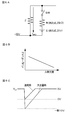
- FIG. 6A is an equivalent circuit diagram showing a breakdown model and a photoelectric conversion model of the SPAD element
- FIG. 6B is a diagram showing a change in the internal impedance of the SPAD element with respect to the amount of incident light
- FIG. It is a waveform figure which shows the cathode potential V CA at the time of light amount.
- FIG. 7 is a circuit diagram showing a configuration example of the light receiving device according to the embodiment of the present disclosure.
- FIG. 8 is a circuit diagram showing a configuration example of the light receiving device according to the first embodiment.
- FIG. 9 is a waveform diagram illustrating a clamping operation when an overvoltage is generated in the light receiving device according to the first embodiment.
- FIG. 10 is a circuit diagram showing an element arrangement example 1 of a SPAD element, a resistance element, a first clamp element, and a second clamp element in a laminated chip structure.
- FIG. 11 is a circuit diagram showing an element arrangement example 2 of a SPAD element, a resistance element, a first clamp element, and a second clamp element in a laminated chip structure.
- FIG. 12 is a circuit diagram showing an element arrangement example 3 of a SPAD element, a resistance element, a first clamp element, and a second clamp element in a laminated chip structure.
- FIG. 13 is a circuit diagram showing a configuration example of the light receiving device according to the second embodiment.
- FIG. 14 is a circuit diagram showing a configuration example of the light receiving device according to the third embodiment.
- FIG. 15 is a circuit diagram showing a configuration example of the light receiving device according to the fourth embodiment.
- FIG. 16 is a circuit diagram showing a configuration example of the light receiving device according to the fifth embodiment.
- FIG. 17 is a circuit diagram showing a configuration example of the light receiving device according to the sixth embodiment.
- FIG. 18 is a circuit diagram showing a configuration example of the light receiving device according to the seventh embodiment.
- FIG. 19 is a circuit diagram showing a configuration example of the light receiving device according to the eighth embodiment.
- FIG. 20 is a circuit diagram showing a configuration example of the light receiving device according to the ninth embodiment.
- FIG. 21 is a block diagram showing an example of a schematic configuration of a vehicle control system, which is an example of a mobile control system to which the technique according to the present disclosure can be applied.
- FIG. 22 is a diagram showing an example of the installation positions of the image pickup unit and the vehicle exterior information detection unit.
- Example 1 (Example of negative bias configuration: Example of protection circuit including clamp circuit) 3-2.
- Example 2 (Modification of Example 1: Example in which the second clamp element is omitted) 3-3.
- Example 3 (Example of negative bias configuration: Example of protection circuit composed of resistance elements) 3-4.
- Example 4 (Modification of Example 1: An example in which the first clamp element is composed of an N-type MOS transistor having a diode connection configuration) 3-5.
- Example 5 (Modification of Example 1: Example in which the first clamp element is composed of a P-type MOS transistor having a diode connection configuration)) 3-6.
- Example 6 (Modification of Example 5: An example in which a resistance element is provided between the gate and drain of a P-type MOS transistor) 3-7.
- Example 7 (Example of positive bias configuration: Example of protection circuit including clamp circuit) 3-8.
- Example 8 (Modification of Example 7: Example in which the second clamp element is omitted) 3-9.
- Example 9 (Example of positive bias configuration: Example in which the protection circuit is composed of a resistance element) 4.
- Application example of the technology according to the present disclosure (example of mobile body) 6. Configuration that can be taken by this disclosure
- the protection circuit may be configured to include a clamp circuit that clamps an overvoltage to a constant voltage.
- the clamp circuit is configured to include a resistance element having one end connected to the light receiving element and a first clamping element connected between the other end of the resistance element and the reference potential node.
- the clamp element may consist of a clamp diode in which the cathode electrode is connected to the other end of the resistance element and the anode electrode is connected to the reference potential node.
- the clamp circuit has a configuration having a second clamp element provided between the first clamp element and the input end of the readout circuit.
- the second clamp element can be configured to consist of a MOS transistor connected between the first clamp element and the input end of the readout circuit and the gate electrode connected to the reference potential node.
- the light receiving device and the distance measuring device of the present disclosure including the above-described preferable configuration have a configuration having a laminated chip structure in which at least two semiconductor substrates, a first semiconductor substrate and a second semiconductor substrate, are laminated. can do. Then, the light receiving element is arranged on the first semiconductor substrate, the resistance element, the first clamping element, and the second clamping element are arranged on the second semiconductor substrate, or the light receiving element and the resistance element are arranged. The first clamping element and the second clamping element are arranged on the first semiconductor substrate, and the light receiving element, the resistance element, and the first clamping element are arranged on the second semiconductor substrate. It can be arranged on the substrate and the second clamping element can be arranged on the second semiconductor substrate.
- the protection circuit may be configured to include a resistance element connected between the light receiving element and the input end of the readout circuit. can. Then, when the N-type MOS transistor connected between the input end of the readout circuit and the reference potential node is provided, the resistance element constituting the protection circuit constitutes the clamp circuit together with the body diode existing in the N-type MOS transistor. Can be done.
- the first clamp element can be configured to include a MOS transistor having a diode connection configuration.
- a second resistance element connected in series with the resistance element, and a P-type MOS connected between the output end of the second resistance element and the reference potential node.
- the gate electrode of the P-type MOS transistor which is composed of a transistor, can be configured to be connected to a common connection node of the resistance element and the second resistance element.
- the readout circuit can be configured to be configured by a CMOS inverter circuit.
- the light receiving element may be configured to be used by applying a voltage equal to or higher than the breakdown voltage. Further, the light receiving element can be configured to include an avalanche photodiode operating in the Geiger mode.
- the light receiving element has a configuration composed of a single photon avalanche diode.
- the single photon avalanche diode can be used by applying a negative bias voltage to the anode electrode, or can be used by applying a positive bias voltage to the cathode electrode.
- FIG. 1 is a schematic configuration diagram showing an example of a distance measuring device (that is, a distance measuring device of the present disclosure) to which the technique according to the present disclosure is applied.
- the distance measuring device 1 according to this application example has a peak wavelength in the infrared wavelength region as a measuring method for measuring the distance to the subject 10 which is the object to be measured.
- the ToF method is used to measure the flight time until the laser beam) is reflected by the subject 10 and returns.
- the distance measuring device 1 according to this application example includes a light source unit 20 and a light receiving device 30. Then, as the light receiving device 30, the light receiving device according to the embodiment of the present disclosure described later can be used.
- the light source unit 20 has, for example, a laser drive unit 21, a laser light source 22, and a diffusion lens 23, and irradiates the subject 10 with a laser beam.
- the laser drive unit 21 drives the laser light source 22 under the control of the control unit 40.
- the laser light source 22 is composed of, for example, a semiconductor laser, and emits laser light when driven by the laser driving unit 21.
- the diffusing lens 23 diffuses the laser light emitted from the laser light source 22 and irradiates the subject 10.
- the light receiving device 30 includes a light receiving lens 31, a light sensor 32 which is a light receiving unit, and a signal processing unit 33, and receives the reflected laser light which is reflected by the subject 10 and returned from the irradiation laser light from the light source unit 20. do.
- the light receiving lens 31 collects the reflected laser light from the subject 10 on the light receiving surface of the light sensor 32.
- the optical sensor 32 receives the reflected laser light from the subject 10 that has passed through the light receiving lens 31 in pixel units and performs photoelectric conversion.
- a two-dimensional array sensor in which pixels including a light receiving element are two-dimensionally arranged in a matrix (array) can be used.
- the output signal of the optical sensor 32 is supplied to the control unit 40 via the signal processing unit 33.
- the control unit 40 is composed of, for example, a CPU (Central Processing Unit) or the like, controls the light source unit 20 and the light receiving device 30, and emits laser light from the light source unit 20 toward the subject 10.
- the time required for the subject 10 to be reflected and returned is measured. Based on this measured time, the distance to the subject 10 can be obtained.
- the timer is started at the timing when the light source unit 20 irradiates the pulsed light, and the timer is stopped at the timing when the light receiving device 30 receives the pulsed light to measure the time.
- pulsed light is irradiated from the light source unit 20 at a predetermined cycle, the cycle when the light receiving device 30 receives the pulsed light is detected, and the phase difference between the light emitting cycle and the light receiving cycle. You may measure the time from.
- the time measurement is executed a plurality of times, and the time is measured by detecting the position of the peak of the ToF histogram obtained by accumulating the times measured a plurality of times.
- the light receiving element of the pixel is an element that generates a signal in response to the light receiving of a photon, for example, a SPAD (Single Photon Avalanche Diode).
- a SPAD Single Photon Avalanche Diode
- a sensor consisting of elements is used. That is, the light receiving device 30 in the distance measuring device 1 according to this application example has a configuration in which a SPAD element is used as the light receiving element of the pixel.
- the SPAD element operates in a Geiger mode in which the element is operated with a reverse voltage exceeding the breakdown voltage (yield voltage).
- the SPAD element is exemplified here as the light receiving element (light detection element) of the pixel, it is not limited to the SPAD element. That is, as the light receiving element of the pixel, in addition to the SPAD element, various elements operating in the Geiger mode such as APD (avalanche photodiode) and SiPM (silicon photomultiplier) can be used.
- APD avalanche photodiode
- SiPM silicon photomultiplier
- FIG. 3 shows an example of the configuration of a basic pixel circuit in the light receiving device 30 using the SPAD element.
- the basic configuration for one pixel is illustrated.
- the cathode electrode of the SPAD element 51 is connected to the terminal 54 to which the power supply voltage V DD is applied via the first control transistor 52 and the current source 53.
- the power supply voltage V DD for example, a voltage of about 3 V is given.
- An anode voltage V ano is applied to the anode electrode of the SPAD element 51.
- the anode voltage V ano a large negative voltage that causes avalanche multiplication, that is, a voltage equal to or higher than the breakdown voltage (for example, about ⁇ 20 V) is applied (see FIG. 4B).
- the first control transistor 52 is composed of, for example, a P-type MOS transistor, and becomes conductive when the enable signal EN applied to the gate electrode becomes low level, and the current from the current source 53 is passed through the MOSFET element 51.
- a second control transistor 55 is connected between the cathode electrode of the SPAD element 51 and the reference potential node (for example, ground).
- the second control transistor 55 is composed of, for example, an N-type MOS transistor, and is in a conductive state when a signal xEN having a phase opposite to that of the enable signal EN is applied to the gate electrode, and the voltage applied to the MOSFET element 51 is a breakdown voltage.
- the SPAD element 51 is put into an inactive state as follows.
- the signal generated by the SPAD element 51 in response to the light reception of photons is read out by the reading circuit 56 as the cathode potential V CA.
- the readout circuit 56 is composed of, for example, a CMOS inverter circuit including a P-type MOS transistor Q p and an N-type MOS transistor Q n , and detects the reaction edge of the MOSFET element 51.
- the output of the read circuit 56 is supplied to the time measuring unit (Time-to-Digital Converter: TDC) 57 as a SPAD output (pixel output). Based on the SPAD output, the time measuring unit 57 measures the time until the light emitted toward the measurement target is reflected by the measurement target and returned.
- TDC Time-to-Digital Converter
- a voltage equal to or higher than the breakdown voltage V BD (for example, about ⁇ 20 V) is applied to the SPAD element 51.
- the excess voltage above the breakdown voltage V BD is called the excess bias voltage V EX. Breakdown voltage
- the characteristics of the SPAD element 51 change depending on how large the excess bias voltage V EX is applied with respect to the voltage value of the BD.
- FIG. 4A illustrates the relationship between the breakdown voltage V BD , the excess bias voltage V EX , and the operating points of the SPAD element 51.
- circuit operation example of a pixel circuit using a SPAD element [Circuit operation example of a pixel circuit using a SPAD element] Subsequently, an example of the circuit operation of the pixel circuit having the above configuration will be described with reference to the waveform diagram of FIG. 4B.
- the cathode potential V CA drops and the voltage between the terminals of the SPAD element 51 becomes the breakdown voltage V BD of the PN diode, the avalanche current stops. Then, generated by avalanche multiplication, the accumulated electrons, the load 54 (e.g., P-type MOS transistor Q L) discharges through, the cathode potential V CA is increased. Then, the cathode potential V CA recovers to the power supply voltage V DD , and returns to the initial state again.
- the load 54 e.g., P-type MOS transistor Q L
- the cathode potential V CA is waveform-shaped by the readout circuit 56 composed of the CMOS inverter circuit, and the pulse signal having the pulse width T starting from the arrival time of one photon is SPAD output (pixel output). It becomes.
- the chip structure of the light receiving device 30 can be a so-called laminated chip structure in which at least two semiconductor substrates, a first semiconductor substrate and a second semiconductor substrate, are laminated. As shown in FIG. 5, the pixels 50 including the SPAD element 51 are arranged in a two-dimensional array of M rows and N columns on the first semiconductor substrate to form a pixel array unit. The first semiconductor substrate on which the pixels 50 are arranged constitutes the sensor chip 101. The sensor chip 101 corresponds to the optical sensor 32 of FIG. 2A.
- a circuit unit 58 is provided for each pixel 50.
- the pixel 50 includes at least the SPAD element 51.
- the circuit unit 58 includes, for example, a first control transistor 52, a current source 53, a second control transistor 55, a read circuit 56, a time measurement unit 57, and the like shown in FIG.
- the circuit unit 58 is arranged on the second semiconductor substrate in a two-dimensional array of M rows and N columns corresponding to each of the pixels 50.
- the second semiconductor substrate on which the circuit unit 58 is arranged constitutes the circuit chip 102.
- the circuit chip 102 is laminated with respect to the sensor chip 101.
- the circuit unit 58 is provided for each pixel 50.
- the readout circuit 56 for detecting the reaction edge of the SPAD element 51 is directly connected to the cathode electrode of the SPAD element 51, and when detecting the reflected light, the amplitude of the voltage set as the Geiger mode is used.
- the circuit configuration is such that a change (for example, about 3V) can be detected.
- FIG. 6A is an equivalent circuit diagram showing a breakdown model and a photoelectric conversion model of the SPAD element 51
- FIG. 6B is a diagram showing a change in the internal impedance of the SPAD element 51 with respect to the amount of incident light
- FIG. 6C is a diagram showing a change in the internal impedance of the SPAD element 51 in a normal state. It is a waveform diagram which shows the cathode potential V CA at the time of (solid line) and a large amount of light (broken line).
- the model of the series circuit of the switch SW, the resistor R, and the voltage source E is the SPAD breakdown model.
- the resistor R of the SPAD element 51 is 20 k ⁇ and the voltage source.
- the model in which E is 20V is illustrated.
- the light intensity dependence is small, and in a normal light intensity of a predetermined light intensity or less, the cathode potential V CA is determined by this SPAD breakdown model.
- the photoelectric conversion model is a model in which the photocurrent I SPAD flows from the second control transistor 55 (see FIG. 3) through the internal impedance Z.
- the internal impedance Z is high, but a large amount of laser light exceeding a predetermined light amount is emitted to the SPAD element 51.
- the internal impedance Z of the SPAD element 51 decreases.
- the internal impedance Z of the SPAD element 51 drops to about 100 ⁇ , and at this time, the cathode potential V CA is calculated. It has been confirmed that there is a possibility of a high potential of -10V or higher.
- the SPAD element 51 when the SPAD element 51 is irradiated with a large amount of laser light, the SPAD element 51 is greatly affected by the photoelectric conversion due to the large amount of light, so that the internal impedance Z is greatly reduced.
- an excessive voltage for example, about several tens of volts
- the P-type MOS transistor Q p and the N-type MOS transistor Q n constituting the read circuit 56, or the first control transistor 52 and the second control transistor 55 Can be destroyed.
- FIG. 7 is a block diagram of a configuration example of the light receiving device according to the embodiment of the present disclosure.
- the SPAD element 51 that generates a signal in response to the light reception of photons
- the readout circuit 56 that reads out the signal generated by the SPAD element 51
- the SPAD element 51 and A protection circuit 60 is provided between the read circuit 56 and the input terminal.
- the protection circuit 60 is a P-type MOS transistor Q p and an N-type MOS transistor Q n constituting the readout circuit 56 from an overvoltage generated when a large amount of laser light is applied to the MOSFET element 51, and a first control. It is an overvoltage protection circuit that acts to protect the transistor 52 and the second control transistor 55.
- the protection circuit 60 when the protection circuit 60 is provided between the SPARC element 51 and the input end of the readout circuit 56, the SPAD element 51 is irradiated with a large amount of laser light equal to or greater than a predetermined amount (more than expected). Even so, due to the action of the protection circuit 60, the P-type MOS transistor Q p and the N-type MOS transistor Q n constituting the read-out circuit 56, and the first control transistor 52 and the second control transistor 55 are removed from the overvoltage. Can be protected.
- the first embodiment is an example of a negative bias configuration, and is an example in which the protection circuit 60 is composed of a clamp circuit.
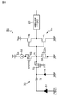
- FIG. 8 shows a circuit diagram of a configuration example of the light receiving device 30 according to the first embodiment.
- the light receiving device 30 according to the first embodiment has a negative bias configuration in which a negative bias voltage (for example, about ⁇ 20 V) is applied to the anode electrode of the SPAD element 51, and the overvoltage is clamped to a constant voltage as the protection circuit 60.
- the configuration uses the clamp circuit 70. That is, in the light receiving device 30 according to the first embodiment, the protection circuit 60 includes a clamp circuit 70 that clamps the overvoltage to a constant voltage.
- the clamp circuit 70 has a structure including a resistance element 71, a first clamp element 72, and a second clamp element 73.
- One end of the resistance element 71 is connected to the cathode electrode of the SPAD element 51.
- the first clamp element 72 is composed of, for example, a clamp diode, the cathode electrode is connected to the other end (output end) of the resistance element 71, and the anode electrode is connected to the reference potential node (for example, ground).
- the resistance element 71 is provided to limit the current value flowing through the clamp diode, which is the first clamp element 72, so as not to exceed the rated forward current of the clamp diode when an overvoltage occurs in the SPAD element 51. ing.
- the first clamp element 72 is not limited to the clamp diode.
- a Schottky barrier diode or the like can be exemplified in addition to the clamp diode.
- the second clamp element 73 is composed of, for example, a P-type MOS transistor, and includes the first clamp element 72 (specifically, the anode electrode of the clamp diode) and the node N to which the input end of the readout circuit 56 is connected. Is connected between.
- the gate electrode is connected to the reference potential node (for example, ground), and the back gate is connected to the source electrode.
- a negative voltage is generated by the clamping operation by the first clamping element 72, and the negative voltage may exceed the withstand voltage of the MOS transistor in the subsequent stage.
- a second clamp element 73 is provided. That is, the second clamping element 73 clamps the voltage of the node N to which the input end of the readout circuit 56 is connected to the gate-source voltage V gs (for example, about 0.5 V) of the P-type MOS transistor.
- V gs for example, about 0.5 V
- an overvoltage generated by irradiating the SPAD element 51 with a large amount of light equal to or more than a predetermined amount by the action of the clamp circuit 70 provided as the protection circuit 60 is generated. It can be clamped to a constant voltage. As a result, the P-type MOS transistor Q p and the N-type MOS transistor Q n constituting the readout circuit 56, and the first control transistor 52 and the second control transistor 55 can be protected from overvoltage.
- the chip structure is a laminated chip structure (see FIG. 5) in which the sensor chip 101 and the circuit chip 102 are laminated as the upper chip and the lower chip.
- the variation of the element arrangement of the SPAD element 51, the resistance element 71, the first clamping element 72, and the second clamping element 73 in the case will be described.
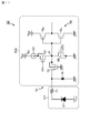
- FIG. 10 is a circuit diagram showing an element arrangement example 1 of the SPAD element 51, the resistance element 71, the first clamp element 72, and the second clamp element 73 in the laminated chip structure.
- the SPAD element 51 is arranged on the sensor chip 101 which is the upper chip, and the resistance element 71 and the first clamping element 72 are arranged on the circuit chip 102 which is the lower chip.
- the second clamp element 73 is arranged, and the first control transistor 52, the current source 53, the second control transistor 55, and the read-out circuit 56 are arranged.
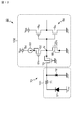
- FIG. 11 is a circuit diagram showing an element arrangement example 2 of the SPAD element 51, the resistance element 71, the first clamp element 72, and the second clamp element 73 in the laminated chip structure.
- the SPAD element 51 and the resistance element 71 are arranged on the sensor chip 101 which is the upper chip, and the first clamping element 72 and the first clamping element 72 and the circuit chip 102 which is the lower chip are arranged.
- a second clamp element 73 is arranged, and a first control transistor 52, a current source 53, a second control transistor 55, and a read-out circuit 56 are arranged.
- FIG. 12 is a circuit diagram showing an element arrangement example 3 of the SPAD element 51, the resistance element 71, the first clamp element 72, and the second clamp element 73 in the laminated chip structure.
- the SPAD element 51, the resistance element 71, and the first clamping element 72 are arranged on the sensor chip 101, which is the upper chip, and the circuit chip 102, which is the lower chip.
- the second clamp element 73, the first control transistor 52, the current source 53, the second control transistor 55, and the read-out circuit 56 are arranged.
- the second embodiment is a modification of the first embodiment, and is an example in which the second clamp element is omitted.
- FIG. 13 shows a circuit diagram of a configuration example of the light receiving device 30 according to the second embodiment.
- the clamp circuit 70 has a resistance element 71 and a first clamp element 72. That is, the light receiving device 30 according to the second embodiment has a configuration in which the second clamp element 73 used as one of the constituent elements of the clamp circuit 70 in the first embodiment is omitted.
- the action and effect of the second clamp element 73 of the first embodiment cannot be obtained, and the voltage of the node N becomes a negative voltage, but an overvoltage (-several tens of volts) is obtained. ) Is extremely low. Therefore, even when a large amount of light equal to or greater than a predetermined amount of light is applied to the MOSFET element 51 and an overvoltage is generated, the P-type MOS transistor Q p and the N-type MOS transistor Q n constituting the readout circuit 56, and the first The control transistor 52 of 1 and the second control transistor 55 can be protected from overvoltage.
- the third embodiment is an example of a negative bias configuration, and is an example in which the protection circuit 60 is composed of a resistance element.
- FIG. 14 shows a circuit diagram of a configuration example of the light receiving device 30 according to the third embodiment.
- the protection circuit 60 is composed of a resistance element 71 connected between the input terminal of the SPAD element 51 and the read circuit 56, that is, the node N. That is, the light receiving device 30 according to the third embodiment has a configuration in which the first clamp element 72 and the second clamp element 73 used as the constituent elements of the clamp circuit 70 in the first embodiment are omitted.
- the resistance element 71 is connected as a second control transistor 55 between the node N to which the input end of the readout circuit 56 is connected and the reference potential node (for example, ground).
- a clamp circuit is formed together with the body diode existing in the N-type MOS transistor.
- the "body diode” is a built-in diode formed by a PN junction between a source and a drain due to the structure of the MOSFET.
- the light receiving device 30 when the SPAD element 51 is irradiated with a large amount of light equal to or more than a predetermined amount of light and an overvoltage occurs, the voltage drops due to the resistance element 71 and the N-type MOS transistor. Due to the clamping action of the body diode of the above, a voltage extremely lower than the overvoltage (-several tens of volts) is applied to the node N.
- the fourth embodiment is a modification of the first embodiment, and is an example in which the first clamp element 73 is configured by using an N-type MOS transistor having a diode connection configuration.
- FIG. 15 shows a circuit diagram of a configuration example of the light receiving device 30 according to the fourth embodiment.
- the first clamp element 72 is composed of an N-type MOS transistor. It is composed.
- the N-type MOS transistor is connected between the other end (output end) of the resistance element 71 and the reference potential node (for example, ground), and has a diode connection configuration in which the gate electrode and the drain electrode are commonly connected. ing.
- the light receiving device 30 uses an N-type MOS transistor having a diode connection configuration as the first clamp element 72 constituting the clamp circuit 70, instead of the clamp diode of the first embodiment. It is composed.
- the same action and effect as in the case of the first embodiment that is, a large amount of light equal to or more than a predetermined amount of light is SPAD.
- the circuit element such as the read circuit 56 in the subsequent stage can be protected from the overvoltage.
- the fifth embodiment is a modification of the first embodiment, and is an example in which the first clamp element 73 is configured by using a P-type MOS transistor having a diode connection configuration.
- FIG. 16 shows a circuit diagram of a configuration example of the light receiving device 30 according to the fifth embodiment.
- the first clamp element 72 is composed of a P-type MOS transistor. It is composed.
- the P-type MOS transistor is connected between the other end (output end) of the resistance element 71 and the reference potential node (for example, ground), and has a diode connection configuration in which the gate electrode and the source electrode are commonly connected. ing.
- the light receiving device 30 uses a P-type MOS transistor having a diode connection configuration as the first clamp element 72 constituting the clamp circuit 70, instead of the clamp diode of the first embodiment. It is composed.
- the same action and effect as in the case of the first embodiment that is, a large amount of light equal to or more than a predetermined amount of light is SPAD.
- the circuit element such as the read circuit 56 in the subsequent stage can be protected from the overvoltage.
- Example 6 is a modification of Example 5, in which a P-type MOS transistor is used as the first clamp element 73 and a resistance element is provided between the gate and drain of the P-type MOS transistor.
- FIG. 17 shows a circuit diagram of a configuration example of the light receiving device 30 according to the sixth embodiment.
- the first clamp element 72 with respect to the resistance element 71. It is composed of a second resistance element 74 connected in series and a P-type MOS transistor connected between the output end of the second resistance element 74 and a reference potential node (for example, ground). ..
- the gate electrode is connected to a common connection node between the resistance element 71 and the second resistance element 74.
- the second resistance element 74 is connected in series to the resistance element 71, and the gate electrode of the P-type MOS transistor is connected to the resistance element 71 and the second resistance element 71. It is configured to be connected to a common connection node with the resistance element 74.
- the P-type MOS transistor can be completely conductive (on state), so that the voltage of the common connection node between the source electrode of the P-type MOS transistor and the output end of the second resistance element 74 is negative. It never becomes a voltage. Therefore, in the case of the sixth embodiment, the second clamp element 73 can be omitted.
- the seventh embodiment is an example of a positive bias configuration, and is an example in which the protection circuit 60 is composed of a clamp circuit.
- FIG. 18 shows a circuit diagram of a configuration example of the light receiving device 30 according to the seventh embodiment.
- the light receiving device 30 according to the seventh embodiment has a positive bias configuration in which a positive bias voltage (for example, about 20 V) is applied to the cathode electrode of the SPAD element 51, and as a protection circuit 60, a clamp that clamps the overvoltage to a constant voltage. It is configured using the circuit 70. That is, the light receiving device 30 according to the seventh embodiment having a positive bias configuration has a circuit configuration corresponding to the light receiving device 30 according to the first embodiment having a negative bias configuration.
- a positive bias voltage for example, about 20 V
- the clamp circuit 70 has a structure including a resistance element 71, a first clamp element 72, and a second clamp element 73.
- One end of the resistance element 71 is connected to the anode electrode of the SPAD element 51.
- the first clamp element 72 is composed of, for example, a clamp diode, the anode electrode is connected to the other end (output end) of the resistance element 71, and the cathode electrode is connected to the node of the power supply voltage V DD.
- the second clamp element 73 is composed of, for example, an N-type MOS transistor, is connected between the first clamp element 72 and the node N, and the gate electrode is connected to the node of the power supply voltage V DD.
- the SPAD element 51 when the SPAD element 51 is irradiated with a large amount of light equal to or more than a predetermined amount by the action of the clamp circuit 70 provided as the protection circuit 60, and an overvoltage occurs. Even so, the read-out circuit 56 in the subsequent stage can be protected from overvoltage. More specifically, the P-type MOS transistor Q p and the N-type MOS transistor Q n constituting the readout circuit 56, and the first control transistor 52 and the second control transistor 55 can be protected from overvoltage.
- Example 8 is a modification of Example 7, and is an example in which the second clamp element is omitted.
- FIG. 19 shows a circuit diagram of a configuration example of the light receiving device 30 according to the eighth embodiment.
- the clamp circuit 70 has a resistance element 71 and a first clamp element 72. That is, the light receiving device 30 according to the eighth embodiment has a configuration in which the second clamp element 73 used as one of the constituent elements of the clamp circuit 70 in the seventh embodiment is omitted, and the negative bias configuration is performed.
- the circuit configuration corresponds to the light receiving device 30 according to 2. Therefore, according to the light receiving device 30 according to the eighth embodiment, basically the same operations and effects as those of the light receiving device 30 according to the second embodiment can be obtained.
- the ninth embodiment is an example of a positive bias configuration, and is an example in which the protection circuit 60 is composed of a resistance element.
- FIG. 20 shows a circuit diagram of a configuration example of the light receiving device 30 according to the ninth embodiment.
- the protection circuit 60 is composed of a resistance element 71 connected between the input terminal of the SPAD element 51 and the read circuit 56, that is, the node N. That is, the light receiving device 30 according to the third embodiment has a configuration in which the first clamp element 72 and the second clamp element 73 used as the constituent elements of the clamp circuit 70 in the first embodiment are omitted, and has a negative bias.
- the circuit configuration corresponds to the light receiving device 30 according to the third embodiment of the configuration. Therefore, according to the light receiving device 30 according to the ninth embodiment, basically the same operations and effects as those of the light receiving device 30 according to the third embodiment can be obtained.
- the first clamp element 72 can have the same configuration as the light receiving device 30 according to the fourth to sixth embodiments having a negative bias configuration. .. That is, the first clamp element 72 can be configured by using a MOS transistor having a diode connection configuration or by combining a second resistance element and a MOS transistor.
- the technology according to the present disclosure can be applied to various products. A more specific application example will be described below.
- the technology according to the present disclosure includes any type of movement such as automobiles, electric vehicles, hybrid electric vehicles, motorcycles, bicycles, personal mobility, airplanes, drones, ships, robots, construction machines, agricultural machines (tractors), and the like. It may be realized as a distance measuring device mounted on the body.
- FIG. 21 is a block diagram showing a schematic configuration example of a vehicle control system 7000, which is an example of a mobile control system to which the technique according to the present disclosure can be applied.
- the vehicle control system 7000 includes a plurality of electronic control units connected via the communication network 7010.
- the vehicle control system 7000 includes a drive system control unit 7100, a body system control unit 7200, a battery control unit 7300, an external information detection unit 7400, an in-vehicle information detection unit 7500, and an integrated control unit 7600. ..
- the communication network 7010 connecting these plurality of control units conforms to any standard such as CAN (Controller Area Network), LIN (Local Interconnect Network), LAN (Local Area Network) or FlexRay (registered trademark). It may be an in-vehicle communication network.
- CAN Controller Area Network
- LIN Local Interconnect Network
- LAN Local Area Network
- FlexRay registered trademark
- Each control unit includes a microcomputer that performs arithmetic processing according to various programs, a storage unit that stores a program executed by the microcomputer or parameters used for various arithmetics, and a drive circuit that drives various control target devices. To be equipped.
- Each control unit is provided with a network I / F for communicating with other control units via the communication network 7010, and is provided by wired communication or wireless communication with devices or sensors inside or outside the vehicle. A communication I / F for performing communication is provided. In FIG.
- control unit 7600 the microcomputer 7610, general-purpose communication I / F 7620, dedicated communication I / F 7630, positioning unit 7640, beacon receiving unit 7650, in-vehicle device I / F 7660, audio image output unit 7670, The vehicle-mounted network I / F 7680 and the storage unit 7690 are shown.
- Other control units also include a microcomputer, a communication I / F, a storage unit, and the like.
- the drive system control unit 7100 controls the operation of the device related to the drive system of the vehicle according to various programs.
- the drive system control unit 7100 provides a driving force generator for generating the driving force of the vehicle such as an internal combustion engine or a driving motor, a driving force transmission mechanism for transmitting the driving force to the wheels, and a steering angle of the vehicle. It functions as a control device such as a steering mechanism for adjusting and a braking device for generating a braking force of a vehicle.
- the drive system control unit 7100 may have a function as a control device such as ABS (Antilock Brake System) or ESC (Electronic Stability Control).
- the vehicle condition detection unit 7110 is connected to the drive system control unit 7100.
- the vehicle state detection unit 7110 may include, for example, a gyro sensor that detects the angular velocity of the axial rotation motion of the vehicle body, an acceleration sensor that detects the acceleration of the vehicle, an accelerator pedal operation amount, a brake pedal operation amount, or steering wheel steering. Includes at least one of the sensors for detecting angular velocity, engine speed, wheel speed, and the like.
- the drive system control unit 7100 performs arithmetic processing using a signal input from the vehicle state detection unit 7110 to control an internal combustion engine, a drive motor, an electric power steering device, a braking device, and the like.
- the body system control unit 7200 controls the operation of various devices mounted on the vehicle body according to various programs.
- the body system control unit 7200 functions as a keyless entry system, a smart key system, a power window device, or a control device for various lamps such as a head lamp, a back lamp, a brake lamp, a winker, or a fog lamp.
- the body system control unit 7200 may be input with radio waves transmitted from a portable device that substitutes for the key or signals of various switches.
- the body system control unit 7200 receives inputs of these radio waves or signals and controls a vehicle door lock device, a power window device, a lamp, and the like.
- the battery control unit 7300 controls the secondary battery 7310, which is the power supply source of the drive motor, according to various programs. For example, information such as the battery temperature, the battery output voltage, or the remaining capacity of the battery is input to the battery control unit 7300 from the battery device including the secondary battery 7310. The battery control unit 7300 performs arithmetic processing using these signals to control the temperature of the secondary battery 7310 or the cooling device provided in the battery device.
- the vehicle outside information detection unit 7400 detects information outside the vehicle equipped with the vehicle control system 7000.
- the imaging unit 7410 and the vehicle exterior information detection unit 7420 is connected to the vehicle exterior information detection unit 7400.
- the imaging unit 7410 includes at least one of a ToF (Time Of Flight) camera, a stereo camera, a monocular camera, an infrared camera, and other cameras.
- the vehicle exterior information detection unit 7420 is used, for example, to detect the current weather or an environmental sensor for detecting the weather, or to detect other vehicles, obstacles, pedestrians, etc. around the vehicle equipped with the vehicle control system 7000. At least one of the ambient information detection sensors is included.
- the environmental sensor may be, for example, at least one of a raindrop sensor that detects rainy weather, a fog sensor that detects fog, a sunshine sensor that detects the degree of sunshine, and a snow sensor that detects snowfall.
- the ambient information detection sensor may be at least one of an ultrasonic sensor, a radar device, and a LIDAR (Light Detection and Ranging, Laser Imaging Detection and Ranging) device.
- the imaging unit 7410 and the vehicle exterior information detection unit 7420 may be provided as independent sensors or devices, or may be provided as a device in which a plurality of sensors or devices are integrated.
- FIG. 22 shows an example of the installation positions of the imaging unit 7410 and the vehicle exterior information detection unit 7420.
- the imaging units 7910, 7912, 7914, 7916, 7918 are provided, for example, at at least one of the front nose, side mirrors, rear bumpers, back door, and upper part of the windshield of the vehicle interior of the vehicle 7900.
- the image pickup unit 7910 provided on the front nose and the image pickup section 7918 provided on the upper part of the windshield in the vehicle interior mainly acquire an image in front of the vehicle 7900.
- the imaging units 7912 and 7914 provided in the side mirrors mainly acquire images of the side of the vehicle 7900.
- the image pickup unit 7916 provided on the rear bumper or the back door mainly acquires an image of the rear of the vehicle 7900.
- the imaging unit 7918 provided on the upper part of the windshield in the vehicle interior is mainly used for detecting a preceding vehicle, a pedestrian, an obstacle, a traffic light, a traffic sign, a lane, or the like.
- FIG. 22 shows an example of the photographing range of each of the imaging units 7910, 7912, 7914, 7916.
- the imaging range a indicates the imaging range of the imaging unit 7910 provided on the front nose
- the imaging ranges b and c indicate the imaging ranges of the imaging units 7912 and 7914 provided on the side mirrors, respectively
- the imaging range d indicates the imaging range d.
- the imaging range of the imaging unit 7916 provided on the rear bumper or the back door is shown. For example, by superimposing the image data captured by the imaging units 7910, 7912, 7914, 7916, a bird's-eye view image of the vehicle 7900 as viewed from above can be obtained.
- the vehicle exterior information detection units 7920, 7922, 7924, 7926, 7928, 7930 provided on the front, rear, side, corners of the vehicle 7900 and the upper part of the windshield in the vehicle interior may be, for example, an ultrasonic sensor or a radar device.
- the vehicle exterior information detection units 7920, 7926, 7930 provided on the front nose, rear bumper, back door, and upper part of the windshield in the vehicle interior of the vehicle 7900 may be, for example, a lidar device.
- These out-of-vehicle information detection units 7920 to 7930 are mainly used for detecting a preceding vehicle, a pedestrian, an obstacle, or the like.
- the vehicle exterior information detection unit 7400 causes the image pickup unit 7410 to capture an image outside the vehicle and receives the captured image data. Further, the vehicle exterior information detection unit 7400 receives detection information from the connected vehicle exterior information detection unit 7420. When the vehicle exterior information detection unit 7420 is an ultrasonic sensor, a radar device, or a lidar device, the vehicle exterior information detection unit 7400 transmits ultrasonic waves, electromagnetic waves, or the like, and receives the received reflected wave information.
- the vehicle exterior information detection unit 7400 may perform object detection processing or distance detection processing such as a person, a vehicle, an obstacle, a sign, or a character on a road surface based on the received information.
- the vehicle exterior information detection unit 7400 may perform an environment recognition process for recognizing rainfall, fog, road surface conditions, etc. based on the received information.
- the vehicle outside information detection unit 7400 may calculate the distance to an object outside the vehicle based on the received information.
- the vehicle exterior information detection unit 7400 may perform image recognition processing or distance detection processing for recognizing a person, a vehicle, an obstacle, a sign, a character on the road surface, or the like based on the received image data.
- the vehicle exterior information detection unit 7400 performs processing such as distortion correction or alignment on the received image data, and synthesizes the image data captured by different imaging units 7410 to generate a bird's-eye view image or a panoramic image. May be good.
- the vehicle exterior information detection unit 7400 may perform the viewpoint conversion process using the image data captured by different imaging units 7410.
- the in-vehicle information detection unit 7500 detects the in-vehicle information.
- a driver state detection unit 7510 that detects the driver's state is connected to the in-vehicle information detection unit 7500.
- the driver state detection unit 7510 may include a camera that captures the driver, a biosensor that detects the driver's biological information, a microphone that collects sound in the vehicle interior, and the like.
- the biosensor is provided on, for example, the seat surface or the steering wheel, and detects the biometric information of the passenger sitting on the seat or the driver holding the steering wheel.
- the in-vehicle information detection unit 7500 may calculate the degree of fatigue or concentration of the driver based on the detection information input from the driver state detection unit 7510, and may determine whether the driver is dozing or not. You may.
- the in-vehicle information detection unit 7500 may perform processing such as noise canceling processing on the collected audio signal.
- the integrated control unit 7600 controls the overall operation in the vehicle control system 7000 according to various programs.
- An input unit 7800 is connected to the integrated control unit 7600.
- the input unit 7800 is realized by a device such as a touch panel, a button, a microphone, a switch or a lever, which can be input-operated by a passenger. Data obtained by recognizing the voice input by the microphone may be input to the integrated control unit 7600.
- the input unit 7800 may be, for example, a remote control device using infrared rays or other radio waves, or an externally connected device such as a mobile phone or a PDA (Personal Digital Assistant) that supports the operation of the vehicle control system 7000. You may.
- the input unit 7800 may be, for example, a camera, in which case the passenger can input information by gesture. Alternatively, data obtained by detecting the movement of the wearable device worn by the passenger may be input. Further, the input unit 7800 may include, for example, an input control circuit that generates an input signal based on the information input by the passenger or the like using the input unit 7800 and outputs the input signal to the integrated control unit 7600. By operating the input unit 7800, the passenger or the like inputs various data to the vehicle control system 7000 and instructs the processing operation.
- the storage unit 7690 may include a ROM (Read Only Memory) for storing various programs executed by the microcomputer, and a RAM (Random Access Memory) for storing various parameters, calculation results, sensor values, and the like. Further, the storage unit 7690 may be realized by a magnetic storage device such as an HDD (Hard Disc Drive), a semiconductor storage device, an optical storage device, an optical magnetic storage device, or the like.
- ROM Read Only Memory
- RAM Random Access Memory
- the general-purpose communication I / F 7620 is a general-purpose communication I / F that mediates communication with various devices existing in the external environment 7750.
- General-purpose communication I / F7620 is a cellular communication protocol such as GSM (registered trademark) (Global System of Mobile communications), WiMAX, LTE (Long Term Evolution) or LTE-A (LTE-Advanced), or wireless LAN (Wi-Fi).
- GSM Global System of Mobile communications
- WiMAX Wireless F
- LTE Long Term Evolution
- LTE-A Long Term Evolution-A
- Wi-Fi wireless LAN
- Other wireless communication protocols such as (also referred to as (registered trademark)) and Bluetooth (registered trademark) may be implemented.
- the general-purpose communication I / F 7620 connects to a device (for example, an application server or a control server) existing on an external network (for example, the Internet, a cloud network, or a business-specific network) via a base station or an access point, for example. You may. Further, the general-purpose communication I / F7620 uses, for example, P2P (Peer To Peer) technology, and is a terminal existing in the vicinity of the vehicle (for example, a terminal of a driver, a pedestrian, or a store, or an MTC (Machine Type Communication) terminal). May be connected with.
- P2P Peer To Peer
- MTC Machine Type Communication
- the dedicated communication I / F 7630 is a communication I / F that supports a communication protocol formulated for use in a vehicle.
- the dedicated communication I / F7630 uses a standard protocol such as WAVE (Wireless Access in Vehicle Environment), DSRC (Dedicated Short Range Communications), or a cellular communication protocol, which is a combination of the lower layer IEEE802.11p and the upper layer IEEE1609. May be implemented.
- the dedicated communication I / F7630 typically includes vehicle-to-vehicle (Vehicle to Vehicle) communication, road-to-vehicle (Vehicle to Infrastructure) communication, vehicle-to-home (Vehicle to Home) communication, and pedestrian-to-pedestrian (Vehicle to Pedestrian) communication. ) Carry out V2X communication, which is a concept that includes one or more of the communications.
- the positioning unit 7640 receives, for example, a GNSS signal from a GNSS (Global Navigation Satellite System) satellite (for example, a GPS signal from a GPS (Global Positioning System) satellite), executes positioning, and executes positioning, and the latitude, longitude, and altitude of the vehicle. Generate location information including.
- the positioning unit 7640 may specify the current position by exchanging signals with the wireless access point, or may acquire position information from a terminal such as a mobile phone, PHS, or smartphone having a positioning function.
- the beacon receiving unit 7650 receives radio waves or electromagnetic waves transmitted from a radio station or the like installed on the road, and acquires information such as the current position, traffic jam, road closure, or required time.
- the function of the beacon receiving unit 7650 may be included in the above-mentioned dedicated communication I / F 7630.
- the in-vehicle device I / F 7660 is a communication interface that mediates the connection between the microcomputer 7610 and various in-vehicle devices 7760 existing in the vehicle.
- the in-vehicle device I / F7660 may establish a wireless connection using a wireless communication protocol such as wireless LAN, Bluetooth (registered trademark), NFC (Near Field Communication) or WUSB (Wireless USB).
- a wireless communication protocol such as wireless LAN, Bluetooth (registered trademark), NFC (Near Field Communication) or WUSB (Wireless USB).
- the in-vehicle device I / F7660 is connected via a connection terminal (and a cable if necessary) (not shown), USB (Universal Serial Bus), HDMI (registered trademark) (High-Definition Multimedia Interface), or MHL (Mobile).
- a wired connection such as High-definition Link may be established.
- the in-vehicle device 7760 may include, for example, at least one of a passenger's mobile device or wearable device, or an information device carried or attached to the vehicle.
- the in-vehicle device 7760 may include a navigation device that searches for a route to an arbitrary destination.
- the in-vehicle device I / F 7660 exchanges control signals or data signals with these in-vehicle devices 7760.
- the in-vehicle network I / F7680 is an interface that mediates communication between the microcomputer 7610 and the communication network 7010.
- the vehicle-mounted network I / F7680 transmits and receives signals and the like according to a predetermined protocol supported by the communication network 7010.
- the microcomputer 7610 of the integrated control unit 7600 is via at least one of general-purpose communication I / F7620, dedicated communication I / F7630, positioning unit 7640, beacon receiving unit 7650, in-vehicle device I / F7660, and in-vehicle network I / F7680. Based on the information acquired in the above, the vehicle control system 7000 is controlled according to various programs. For example, the microcomputer 7610 calculates the control target value of the driving force generator, the steering mechanism, or the braking device based on the acquired information inside and outside the vehicle, and outputs a control command to the drive system control unit 7100. May be good.
- the microcomputer 7610 realizes ADAS (Advanced Driver Assistance System) functions including vehicle collision avoidance or impact mitigation, follow-up driving based on inter-vehicle distance, vehicle speed maintenance driving, vehicle collision warning, vehicle lane deviation warning, and the like. Cooperative control may be performed for the purpose of.
- the microcomputer 7610 automatically travels autonomously without relying on the driver's operation by controlling the driving force generator, steering mechanism, braking device, etc. based on the acquired information on the surroundings of the vehicle. Coordinated control for the purpose of driving or the like may be performed.
- ADAS Advanced Driver Assistance System
- the microcomputer 7610 has information acquired via at least one of general-purpose communication I / F7620, dedicated communication I / F7630, positioning unit 7640, beacon receiving unit 7650, in-vehicle device I / F7660, and in-vehicle network I / F7680. Based on the above, three-dimensional distance information between the vehicle and an object such as a surrounding structure or a person may be generated, and local map information including the peripheral information of the current position of the vehicle may be created. Further, the microcomputer 7610 may predict a danger such as a vehicle collision, a pedestrian or the like approaching or entering a closed road based on the acquired information, and may generate a warning signal.
- the warning signal may be, for example, a signal for generating a warning sound or turning on a warning lamp.
- the audio image output unit 7670 transmits the output signal of at least one of the audio and the image to the output device capable of visually or audibly notifying the passenger or the outside of the vehicle of the information.
- an audio speaker 7710, a display unit 7720, and an instrument panel 7730 are exemplified as output devices.
- the display unit 7720 may include, for example, at least one of an onboard display and a heads-up display.
- the display unit 7720 may have an AR (Augmented Reality) display function.
- the output device may be other devices other than these devices, such as headphones, wearable devices such as eyeglass-type displays worn by passengers, and projectors or lamps.
- the display device displays the results obtained by various processes performed by the microcomputer 7610 or the information received from other control units in various formats such as texts, images, tables, and graphs. Display visually.
- the audio output device converts an audio signal composed of reproduced audio data, acoustic data, or the like into an analog signal and outputs the audio signal audibly.
- At least two control units connected via the communication network 7010 may be integrated as one control unit.
- each control unit may be composed of a plurality of control units.
- the vehicle control system 7000 may include another control unit (not shown).
- the other control unit may have a part or all of the functions carried out by any of the control units. That is, as long as information is transmitted and received via the communication network 7010, predetermined arithmetic processing may be performed by any control unit.
- a sensor or device connected to any control unit may be connected to another control unit, and a plurality of control units may send and receive detection information to and from each other via the communication network 7010. .
- the imaging unit 7410 or the vehicle exterior information detection unit 7420 includes a ToF camera (ToF sensor)
- the ToF camera receives light according to the above-described embodiment.
- the device can be used.
- the light receiving device as a ToF camera of a distance measuring device, for example, when a large amount of light exceeding a predetermined amount of light is irradiated to the light receiving element and an overvoltage occurs in the light receiving element, the element is destroyed by the overvoltage. Since it can be blocked, a highly reliable vehicle control system can be constructed.
- the present disclosure may also have the following configuration.
- a light receiving element that generates a signal in response to the light received by a photon
- a readout circuit that reads out the signal generated by the light receiving element
- a protection circuit provided between the light receiving element and the input end of the readout circuit to protect the circuit element of the readout circuit from overvoltage.
- a light receiving device comprising.
- the protection circuit consists of a clamp circuit that clamps the overvoltage to a constant voltage.
- the clamp circuit is A resistance element with one end connected to the light receiving element, and A first clamp element connected between the other end of the resistance element and the reference potential node, Have, The light receiving device according to the above [A-2].
- the first clamp element comprises a clamp diode in which the cathode electrode is connected to the other end of the resistance element and the anode electrode is connected to the reference potential node.
- the clamp circuit is a second clamp element provided between the first clamp element and the input end of the readout circuit. Have, The light receiving device according to the above [A-3] or the above [A-4].
- the second clamp element is composed of a MOS transistor connected between the first clamp element and the input end of the readout circuit, and the gate electrode is connected to the reference potential node. The light receiving device according to the above [A-5].
- [A-7] It has a laminated chip structure in which at least two semiconductor substrates, a first semiconductor substrate and a second semiconductor substrate, are laminated.
- the light receiving element is arranged on the first semiconductor substrate and is arranged on the first semiconductor substrate.
- the resistance element, the first clamp element, and the second clamp element are arranged on the second semiconductor substrate.
- the light receiving device according to the above [A-5] or the above [A-6].
- [A-8] It has a laminated chip structure in which at least two semiconductor substrates, a first semiconductor substrate and a second semiconductor substrate, are laminated.
- the light receiving element and the resistance element are arranged on the first semiconductor substrate, and the light receiving element and the resistance element are arranged on the first semiconductor substrate.
- the first clamp element and the second clamp element are arranged on the second semiconductor substrate.
- the light receiving device according to the above [A-5] or the above [A-6].
- [A-9] It has a laminated chip structure in which at least two semiconductor substrates, a first semiconductor substrate and a second semiconductor substrate, are laminated. The light receiving element, the resistance element, and the first clamp element are arranged on the first semiconductor substrate. The second clamp element is arranged on the second semiconductor substrate, The light receiving device according to the above [A-5] or the above [A-6].
- the protection circuit consists of a resistance element connected between the light receiving element and the input end of the readout circuit. The light receiving device according to the above [A-1].
- the resistance element that constitutes the protection circuit constitutes the clamp circuit together with the body diode that exists in the N-type MOS transistor.
- the first clamp element is composed of a MOS transistor having a diode connection configuration.
- the first clamp element is A second resistance element connected in series with the resistance element, and It consists of a P-type MOS transistor connected between the output end of the second resistance element and the reference potential node.
- the gate electrode of the P-type MOS transistor is connected to the common connection node of the resistance element and the second resistance element.
- the light receiving device according to the above [A-3].
- the readout circuit is composed of a CMOS inverter circuit.
- the light receiving device according to any one of the above [A-1] to the above [A-13].
- the light receiving element is an element used by applying a voltage equal to or higher than the breakdown voltage.
- the light receiving device according to any one of the above [A-1] to the above [A-14].
- the light receiving element comprises an avalanche photodiode operating in Geiger mode.
- the light receiving device according to the above [A-15].
- the light receiving element is composed of a single photon avalanche diode.
- the light receiving device according to the above [A-16].
- a single photon avalanche diode is used by applying a negative bias voltage to the anode electrode.
- a single photon avalanche diode is used by applying a positive bias voltage to the cathode electrode.
- a light source unit that irradiates a distance measuring object with light
- a light receiving device that receives reflected light from a distance measuring object based on the irradiation light from the light source unit. Equipped with The light receiving device is A light receiving element that generates a signal in response to the light received by a photon, A readout circuit that reads out the signal generated by the light receiving element, and A protection circuit provided between the light receiving element and the readout circuit to protect the circuit element of the readout circuit from overvoltage.
- the protection circuit consists of a clamp circuit that clamps the overvoltage to a constant voltage. The distance measuring device according to the above [B-1].
- the clamp circuit is A resistance element with one end connected to the light receiving element, and A first clamp element connected between the other end of the resistance element and the reference potential node, Have, The distance measuring device according to the above [B-2].
- the first clamp element comprises a clamp diode in which the cathode electrode is connected to the other end of the resistance element and the anode electrode is connected to the reference potential node.
- the clamp circuit is a second clamp element provided between the first clamp element and the input end of the readout circuit. Have, The distance measuring device according to the above [B-3] or the above [B-4].
- the second clamp element is composed of a MOS transistor connected between the first clamp element and the input end of the readout circuit, and the gate electrode is connected to the reference potential node.
- [B-7] It has a laminated chip structure in which at least two semiconductor substrates, a first semiconductor substrate and a second semiconductor substrate, are laminated.
- the light receiving element is arranged on the first semiconductor substrate and is arranged on the first semiconductor substrate.
- the resistance element, the first clamp element, and the second clamp element are arranged on the second semiconductor substrate.
- [B-8] It has a laminated chip structure in which at least two semiconductor substrates, a first semiconductor substrate and a second semiconductor substrate, are laminated.
- the light receiving element and the resistance element are arranged on the first semiconductor substrate, and the light receiving element and the resistance element are arranged on the first semiconductor substrate.
- the first clamp element and the second clamp element are arranged on the second semiconductor substrate.
- the distance measuring device according to the above [B-5] or the above [B-6].
- [B-9] It has a laminated chip structure in which at least two semiconductor substrates, a first semiconductor substrate and a second semiconductor substrate, are laminated. The light receiving element, the resistance element, and the first clamp element are arranged on the first semiconductor substrate.
- the second clamp element is arranged on the second semiconductor substrate, The distance measuring device according to the above [B-5] or the above [B-6].
- the protection circuit consists of a resistance element connected between the light receiving element and the input end of the readout circuit.
- [B-11] Having an N-type MOS transistor connected between the input end of the readout circuit and the reference potential node, The resistance element that constitutes the protection circuit constitutes the clamp circuit together with the body diode that exists in the N-type MOS transistor.
- the first clamp element is composed of a MOS transistor having a diode connection configuration. The distance measuring device according to the above [B-3].
- the first clamp element is A second resistance element connected in series with the resistance element, and It consists of a P-type MOS transistor connected between the output end of the second resistance element and the reference potential node.
- the gate electrode of the P-type MOS transistor is connected to the common connection node of the resistance element and the second resistance element.
- the readout circuit is composed of a CMOS inverter circuit.
- the light receiving element is an element used by applying a voltage equal to or higher than the breakdown voltage. The distance measuring device according to any one of the above [B-1] to the above [B-14].
- the light receiving element comprises an avalanche photodiode operating in Geiger mode.
- the light receiving element is composed of a single photon avalanche diode.
- a single photon avalanche diode is used by applying a negative bias voltage to the anode electrode.
- [B-19] A single photon avalanche diode is used by applying a positive bias voltage to the cathode electrode.
- ranging device 10 ... subject, 20 ... light source unit, 21 ... laser drive unit, 22 ... laser light source, 23 ... diffuser lens, 30 ... light receiving device, 31 ... Light receiving lens, 32 ... Optical sensor, 33 ... Signal processing unit, 40 ... Control unit, 50 ... Pixel, 51 ... SPAD element, 56 ... Read circuit, 57 ... Time measurement unit (TDC), 60 ... Protection circuit, 70 ... Clamp circuit
Landscapes
- Physics & Mathematics (AREA)
- Engineering & Computer Science (AREA)
- General Physics & Mathematics (AREA)
- Radar, Positioning & Navigation (AREA)
- Remote Sensing (AREA)
- Electromagnetism (AREA)
- Computer Networks & Wireless Communication (AREA)
- Spectroscopy & Molecular Physics (AREA)
- Light Receiving Elements (AREA)
- Optical Radar Systems And Details Thereof (AREA)
- Solid State Image Pick-Up Elements (AREA)
Abstract
Description
光子の受光に応じて信号を発生する受光素子、
受光素子が発生する信号を読み出す読出し回路、及び、
受光素子と読出し回路との間に設けられ、読出し回路の回路素子を過電圧から保護する保護回路、
を備える。
測距対象物に対して光を照射する光源部、及び、
光源部からの照射光に基づく、測距対象物からの反射光を受光する受光装置、
を具備する。
そして、受光装置は、
光子の受光に応じて信号を発生する受光素子、
受光素子が発生する信号を読み出す読出し回路、及び、
受光素子と読出し回路との間に設けられ、読出し回路の回路素子を過電圧から保護する保護回路、
を備える。
1.本開示の受光装置及び測距装置、全般に関する説明
2.本開示に係る技術が適用される測距装置
2-1.測距装置の具体的な構成例
2-2.SPAD素子を用いた基本的な画素回路例
2-3.SPAD素子を用いた画素回路の回路動作例
2-4.SPAD素子の読出し回路に印加される過電圧について
3.本開示の実施形態に係る受光装置
3-1.実施例1(負バイアス構成の例:保護回路がクランプ回路から成る例)
3-2.実施例2(実施例1の変形例:第2のクランプ素子を省略した例)
3-3.実施例3(負バイアス構成の例:保護回路が抵抗素子から成る例)
3-4.実施例4(実施例1の変形例:第1のクランプ素子をダイオード接続構成のN型MOSトランジスタで構成する例)
3-5.実施例5(実施例1の変形例:第1のクランプ素子をダイオード接続構成のP型MOSトランジスタで構成する例))
3-6.実施例6(実施例5の変形例:P型MOSトランジスタのゲート-ドレイン間に抵抗素子を設ける例)
3-7.実施例7(正バイアス構成の例:保護回路がクランプ回路から成る例)
3-8.実施例8(実施例7の変形例:第2のクランプ素子を省略した例)
3-9.実施例9(正バイアス構成の例:保護回路が抵抗素子から成る例)
4.変形例
5.本開示に係る技術の適用例(移動体の例)
6.本開示がとることができる構成
本開示の受光装置及び測距装置にあっては、保護回路について、過電圧を一定の電圧にクランプするクランプ回路から成る構成とすることができる。そして、クランプ回路について、受光素子に対して一端が接続された抵抗素子、及び、抵抗素子の他端と基準電位ノードとの間に接続された第1のクランプ素子を有する構成とし、第1のクランプ素子について、カソード電極が抵抗素子の他端に接続され、アノード電極が基準電位ノードに接続されたクランプダイオードから成る構成とすることができる。
図1は、本開示に係る技術が適用される測距装置(即ち、本開示の測距装置)の一例を示す概略構成図である。
本適用例に係る測距装置1の具体的な構成の一例を図2A及び図2Bに示す。光源部20は、例えば、レーザ駆動部21、レーザ光源22、及び、拡散レンズ23を有し、被写体10に対してレーザ光を照射する。レーザ駆動部21は、制御部40による制御の下に、レーザ光源22を駆動する。レーザ光源22は、例えば半導体レーザから成り、レーザ駆動部21によって駆動されることによってレーザ光を出射する。拡散レンズ23は、レーザ光源22から出射されたレーザ光を拡散し、被写体10に対して照射する。
SPAD素子を用いた受光装置30における基本的な画素回路の構成の一例を図3に示す。ここでは、1画素分の基本構成を図示している。
続いて、上記の構成の画素回路の回路動作の一例について、図4Bの波形図を用いて説明する。
受光装置30のチップ構造としては、所謂、第1半導体基板及び第2半導体基板の少なくとも2つの半導体基板が積層されて成る積層型チップ構造とすることができる。SPAD素子51を含む画素50は、図5に示すように、第1半導体基板上に、M行N列の2次元アレイ状に配置されて画素アレイ部を構成している。画素50が配置されて成る第1半導体基板は、センサチップ101を構成している。このセンサチップ101は、図2Aの光センサ32に相当する。
上記の例の場合、SPAD素子51の反応エッジを検出する読出し回路56は、SPAD素子51のカソード電極に直接接続されており、反射光を検出する場合はガイガーモードとして設定される電圧の振幅の変化(例えば、3V程度)を検出できるような回路構成になっている。
図7は、本開示の実施形態に係る受光装置の構成例をブロック図である。図7に示すように、本実施形態では、光子の受光に応じて信号を発生するSPAD素子51、及び、SPAD素子51が発生する信号を読み出す読出し回路56を備える受光装置において、SPAD素子51と読出し回路56の入力端との間に、保護回路60を設けた構成となっている。
実施例1は、負バイアス構成の例であり、保護回路60がクランプ回路から成る例である。実施例1に係る受光装置30の構成例の回路図を図8に示す。
図10は、積層型チップ構造におけるSPAD素子51、抵抗素子71、第1のクランプ素子72、及び、第2のクランプ素子73の素子配置例1を示す回路図である。
図11は、積層型チップ構造におけるSPAD素子51、抵抗素子71、第1のクランプ素子72、及び、第2のクランプ素子73の素子配置例2を示す回路図である。
図12は、積層型チップ構造におけるSPAD素子51、抵抗素子71、第1のクランプ素子72、及び、第2のクランプ素子73の素子配置例3を示す回路図である。
実施例2は、実施例1の変形例であり、第2のクランプ素子を省略した例である。実施例2に係る受光装置30の構成例の回路図を図13に示す。
実施例3は、負バイアス構成の例であり、保護回路60が抵抗素子から成る例である。実施例3に係る受光装置30の構成例の回路図を図14に示す。
実施例4は、実施例1の変形例であり、第1のクランプ素子73を、ダイオード接続構成のN型MOSトランジスタを用いて構成する例である。実施例4に係る受光装置30の構成例の回路図を図15に示す。
実施例5は、実施例1の変形例であり、第1のクランプ素子73を、ダイオード接続構成のP型MOSトランジスタを用いて構成する例である。実施例5に係る受光装置30の構成例の回路図を図16に示す。
実施例6は、実施例5の変形例であり、第1のクランプ素子73としてP型MOSトランジスタを用い、P型MOSトランジスタのゲート-ドレイン間に抵抗素子を設ける例である。実施例6に係る受光装置30の構成例の回路図を図17に示す。
実施例7は、正バイアス構成の例であり、保護回路60がクランプ回路から成る例である。実施例7に係る受光装置30の構成例の回路図を図18に示す。
実施例8は、実施例7の変形例であり、第2のクランプ素子を省略した例である。実施例8に係る受光装置30の構成例の回路図を図19に示す。
実施例9は、正バイアス構成の例であり、保護回路60が抵抗素子から成る例である。実施例9に係る受光装置30の構成例の回路図を図20に示す。
以上、本開示に係る技術について、好ましい実施形態に基づき説明したが、本開示に係る技術は当該実施形態に限定されるものではない。上記の実施形態において説明した受光装置及び測距装置の構成、構造は例示であり、適宜、変更することができる。
本開示に係る技術は、様々な製品に適用することができる。以下に、より具体的な適用例について説明する。例えば、本開示に係る技術は、自動車、電気自動車、ハイブリッド電気自動車、自動二輪車、自転車、パーソナルモビリティ、飛行機、ドローン、船舶、ロボット、建設機械、農業機械(トラクター)などのいずれかの種類の移動体に搭載される測距装置として実現されてもよい。
図21は、本開示に係る技術が適用され得る移動体制御システムの一例である車両制御システム7000の概略的な構成例を示すブロック図である。車両制御システム7000は、通信ネットワーク7010を介して接続された複数の電子制御ユニットを備える。図21に示した例では、車両制御システム7000は、駆動系制御ユニット7100、ボディ系制御ユニット7200、バッテリ制御ユニット7300、車外情報検出ユニット7400、車内情報検出ユニット7500、及び統合制御ユニット7600を備える。これらの複数の制御ユニットを接続する通信ネットワーク7010は、例えば、CAN(Controller Area Network)、LIN(Local Interconnect Network)、LAN(Local Area Network)又はFlexRay(登録商標)等の任意の規格に準拠した車載通信ネットワークであってよい。
尚、本開示は、以下のような構成をとることもできる。
[A-1]光子の受光に応じて信号を発生する受光素子、
受光素子が発生する信号を読み出す読出し回路、及び、
受光素子と読出し回路の入力端との間に設けられ、読出し回路の回路素子を過電圧から保護する保護回路、
を備える受光装置。
[A-2]保護回路は、過電圧を一定の電圧にクランプするクランプ回路から成る、
上記[A-1]に記載の受光装置。
[A-3]クランプ回路は、
受光素子に対して一端が接続された抵抗素子、及び、
抵抗素子の他端と基準電位ノードとの間に接続された第1のクランプ素子、
を有する、
上記[A-2]に記載の受光装置。
[A-4]第1のクランプ素子は、カソード電極が抵抗素子の他端に接続され、アノード電極が基準電位ノードに接続されたクランプダイオードから成る、
上記[A-3]に記載の受光装置。
[A-5]クランプ回路は、第1のクランプ素子と読出し回路の入力端との間に設けられた第2のクランプ素子、
を有する、
上記[A-3]又は上記[A-4]に記載の受光装置。
[A-6]第2のクランプ素子は、第1のクランプ素子と読出し回路の入力端との間に接続され、ゲート電極が基準電位ノードに接続されたMOSトランジスタから成る、
上記[A-5]に記載の受光装置。
[A-7]第1半導体基板及び第2半導体基板の少なくとも2つの半導体基板が積層されて成る積層型チップ構造を有し、
受光素子は、第1半導体基板に配置され、
抵抗素子、第1のクランプ素子、及び、第2のクランプ素子は、第2半導体基板に配置されている、
上記[A-5]又は上記[A-6]に記載の受光装置。
[A-8]第1半導体基板及び第2半導体基板の少なくとも2つの半導体基板が積層されて成る積層型チップ構造を有し、
受光素子及び抵抗素子は、第1半導体基板に配置され、
第1のクランプ素子及び第2のクランプ素子は、第2半導体基板に配置されている、
上記[A-5]又は上記[A-6]に記載の受光装置。
[A-9]第1半導体基板及び第2半導体基板の少なくとも2つの半導体基板が積層されて成る積層型チップ構造を有し、
受光素子、抵抗素子、及び、第1のクランプ素子は、第1半導体基板に配置され、
第2のクランプ素子は、第2半導体基板に配置されている、
上記[A-5]又は上記[A-6]に記載の受光装置。
[A-10]保護回路は、受光素子と読出し回路の入力端との間に接続された抵抗素子から成る、
上記[A-1]に記載の受光装置。
[A-11]読出し回路の入力端と基準電位ノードとの間に接続されたN型MOSトランジスタを有し、
保護回路を構成する抵抗素子は、N型MOSトランジスタに存在するボディダイオードと共にクランプ回路を構成する、
上記[A-10]に記載の受光装置。
[A-12]第1のクランプ素子は、ダイオード接続構成のMOSトランジスタから成る、
上記[A-3]に記載の受光装置。
[A-13]第1のクランプ素子は、
抵抗素子に対して直列に接続された第2の抵抗素子、及び、
第2の抵抗素子の出力端と基準電位ノードとの間に接続されたP型MOSトランジスタから成り、
P型MOSトランジスタのゲート電極は、抵抗素子と第2の抵抗素子との共通接続ノードに接続されている、
上記[A-3]に記載の受光装置。
[A-14]読出し回路は、CMOSインバータ回路によって構成されている、
上記[A-1]乃至上記[A-13]のいずれかに記載の受光装置。
[A-15]受光素子は、ブレークダウン電圧以上の電圧が印加されて使用される素子である、
上記[A-1]乃至上記[A-14]のいずれかに記載の受光装置。
[A-16]受光素子は、ガイガーモードで動作するアバランシェフォトダイオードから成る、
上記[A-15]に記載の受光装置。
[A-17]受光素子は、単一光子アバランシェダイオードから成る、
上記[A-16]に記載の受光装置。
[A-18]単一光子アバランシェダイオードは、アノード電極に負のバイアス電圧が印加されて用いられる、
上記[A-17]に記載の受光装置。
[A-19]単一光子アバランシェダイオードは、カソード電極に正のバイアス電圧が印加されて用いられる、
上記[A-17]に記載の受光装置。
[B-1]測距対象物に対して光を照射する光源部、及び、
光源部からの照射光に基づく、測距対象物からの反射光を受光する受光装置、
を具備し、
受光装置は、
光子の受光に応じて信号を発生する受光素子、
受光素子が発生する信号を読み出す読出し回路、及び、
受光素子と読出し回路との間に設けられ、読出し回路の回路素子を過電圧から保護する保護回路、
を備える測距装置。
[B-2]保護回路は、過電圧を一定の電圧にクランプするクランプ回路から成る、
上記[B-1]に記載の測距装置。
[B-3]クランプ回路は、
受光素子に対して一端が接続された抵抗素子、及び、
抵抗素子の他端と基準電位ノードとの間に接続された第1のクランプ素子、
を有する、
上記[B-2]に記載の測距装置。
[B-4]第1のクランプ素子は、カソード電極が抵抗素子の他端に接続され、アノード電極が基準電位ノードに接続されたクランプダイオードから成る、
上記[B-3]に記載の測距装置。
[B-5]クランプ回路は、第1のクランプ素子と読出し回路の入力端との間に設けられた第2のクランプ素子、
を有する、
上記[B-3]又は上記[B-4]に記載の測距装置。
[B-6]第2のクランプ素子は、第1のクランプ素子と読出し回路の入力端との間に接続され、ゲート電極が基準電位ノードに接続されたMOSトランジスタから成る、
上記[B-5]に記載の測距装置。
[B-7]第1半導体基板及び第2半導体基板の少なくとも2つの半導体基板が積層されて成る積層型チップ構造を有し、
受光素子は、第1半導体基板に配置され、
抵抗素子、第1のクランプ素子、及び、第2のクランプ素子は、第2半導体基板に配置されている、
上記[B-5]又は上記[B-6]に記載の測距装置。
[B-8]第1半導体基板及び第2半導体基板の少なくとも2つの半導体基板が積層されて成る積層型チップ構造を有し、
受光素子及び抵抗素子は、第1半導体基板に配置され、
第1のクランプ素子及び第2のクランプ素子は、第2半導体基板に配置されている、
上記[B-5]又は上記[B-6]に記載の測距装置。
[B-9]第1半導体基板及び第2半導体基板の少なくとも2つの半導体基板が積層されて成る積層型チップ構造を有し、
受光素子、抵抗素子、及び、第1のクランプ素子は、第1半導体基板に配置され、
第2のクランプ素子は、第2半導体基板に配置されている、
上記[B-5]又は上記[B-6]に記載の測距装置。
[B-10]保護回路は、受光素子と読出し回路の入力端との間に接続された抵抗素子から成る、
上記[B-1]に記載の測距装置。
[B-11]読出し回路の入力端と基準電位ノードとの間に接続されたN型MOSトランジスタを有し、
保護回路を構成する抵抗素子は、N型MOSトランジスタに存在するボディダイオードと共にクランプ回路を構成する、
上記[B-10]に記載の測距装置。
[B-12]第1のクランプ素子は、ダイオード接続構成のMOSトランジスタから成る、
上記[B-3]に記載の測距装置。
[B-13]第1のクランプ素子は、
抵抗素子に対して直列に接続された第2の抵抗素子、及び、
第2の抵抗素子の出力端と基準電位ノードとの間に接続されたP型MOSトランジスタから成り、
P型MOSトランジスタのゲート電極は、抵抗素子と第2の抵抗素子との共通接続ノードに接続されている、
上記[B-3]に記載の測距装置。
[B-14]読出し回路は、CMOSインバータ回路によって構成されている、
上記[B-1]乃至上記[B-13]のいずれかに記載の測距装置。
[B-15]受光素子は、ブレークダウン電圧以上の電圧が印加されて使用される素子である、
上記[B-1]乃至上記[B-14]のいずれかに記載の測距装置。
[B-16]受光素子は、ガイガーモードで動作するアバランシェフォトダイオードから成る、
上記[B-15]に記載の測距装置。
[B-17]受光素子は、単一光子アバランシェダイオードから成る、
上記[B-16]に記載の測距装置。
[B-18]単一光子アバランシェダイオードは、アノード電極に負のバイアス電圧が印加されて用いられる、
上記[B-17]に記載の測距装置。
[B-19]単一光子アバランシェダイオードは、カソード電極に正のバイアス電圧が印加されて用いられる、
上記[B-17]に記載の測距装置。
Claims (20)
- 光子の受光に応じて信号を発生する受光素子、
受光素子が発生する信号を読み出す読出し回路、及び、
受光素子と読出し回路の入力端との間に設けられ、読出し回路の回路素子を過電圧から保護する保護回路、
を備える受光装置。 - 保護回路は、過電圧を一定の電圧にクランプするクランプ回路から成る、
請求項1に記載の受光装置。 - クランプ回路は、
受光素子に対して一端が接続された抵抗素子、及び、
抵抗素子の他端と基準電位ノードとの間に接続された第1のクランプ素子、
を有する、
請求項2に記載の受光装置。 - 第1のクランプ素子は、カソード電極が抵抗素子の他端に接続され、アノード電極が基準電位ノードに接続されたクランプダイオードから成る、
請求項3に記載の受光装置。 - クランプ回路は、第1のクランプ素子と読出し回路の入力端との間に設けられた第2のクランプ素子、
を有する、
請求項3に記載の受光装置。 - 第2のクランプ素子は、第1のクランプ素子と読出し回路の入力端との間に接続され、ゲート電極が基準電位ノードに接続されたMOSトランジスタから成る、
請求項5に記載の受光装置。 - 第1半導体基板及び第2半導体基板の少なくとも2つの半導体基板が積層されて成る積層型チップ構造を有し、
受光素子は、第1半導体基板に配置され、
抵抗素子、第1のクランプ素子、及び、第2のクランプ素子は、第2半導体基板に配置されている、
請求項5に記載の受光装置。 - 第1半導体基板及び第2半導体基板の少なくとも2つの半導体基板が積層されて成る積層型チップ構造を有し、
受光素子及び抵抗素子は、第1半導体基板に配置され、
第1のクランプ素子及び第2のクランプ素子は、第2半導体基板に配置されている、
請求項5に記載の受光装置。 - 第1半導体基板及び第2半導体基板の少なくとも2つの半導体基板が積層されて成る積層型チップ構造を有し、
受光素子、抵抗素子、及び、第1のクランプ素子は、第1半導体基板に配置され、
第2のクランプ素子は、第2半導体基板に配置されている、
請求項5に記載の受光装置。 - 保護回路は、受光素子と読出し回路の入力端との間に接続された抵抗素子から成る、
請求項1に記載の受光装置。 - 読出し回路の入力端と基準電位ノードとの間に接続されたN型MOSトランジスタを有し、
保護回路を構成する抵抗素子は、N型MOSトランジスタに存在するボディダイオードと共にクランプ回路を構成する、
請求項10に記載の受光装置。 - 第1のクランプ素子は、ダイオード接続構成のMOSトランジスタから成る、
請求項3に記載の受光装置。 - 第1のクランプ素子は、
抵抗素子に対して直列に接続された第2の抵抗素子、及び、
第2の抵抗素子の出力端と基準電位ノードとの間に接続されたP型MOSトランジスタから成り、
P型MOSトランジスタのゲート電極は、抵抗素子と第2の抵抗素子との共通接続ノードに接続されている、
請求項3に記載の受光装置。 - 読出し回路は、CMOSインバータ回路によって構成されている、
請求項1に記載の受光装置。 - 受光素子は、ブレークダウン電圧以上の電圧が印加されて使用される素子である、
請求項1に記載の受光装置。 - 受光素子は、ガイガーモードで動作するアバランシェフォトダイオードから成る、
請求項15に記載の受光装置。 - 受光素子は、単一光子アバランシェダイオードから成る、
請求項16に記載の受光装置。 - 単一光子アバランシェダイオードは、アノード電極に負のバイアス電圧が印加されて用いられる、
請求項17に記載の受光装置。 - 単一光子アバランシェダイオードは、カソード電極に正のバイアス電圧が印加されて用いられる、
請求項17に記載の受光装置。 - 測距対象物に対して光を照射する光源部、及び、
光源部からの照射光に基づく、測距対象物からの反射光を受光する受光装置、
を具備し、
受光装置は、
光子の受光に応じて信号を発生する受光素子、
受光素子が発生する信号を読み出す読出し回路、及び、
受光素子と読出し回路との間に設けられ、読出し回路の回路素子を過電圧から保護する保護回路、
を備える測距装置。
Priority Applications (8)
| Application Number | Priority Date | Filing Date | Title |
|---|---|---|---|
| JP2022509422A JP7673049B2 (ja) | 2020-03-24 | 2021-02-20 | 受光装置及び測距装置 |
| KR1020227031531A KR20220156541A (ko) | 2020-03-24 | 2021-02-20 | 수광 장치 및 측거 장치 |
| US17/912,251 US11725983B2 (en) | 2020-03-24 | 2021-02-20 | Light receiving device and distance measuring device comprising a circuit to protect a circuit element of a readout circuit from overvoltage |
| EP25205050.5A EP4648579A3 (en) | 2020-03-24 | 2021-02-20 | Light receiving device and distance measuring device |
| EP21776224.4A EP4130657B1 (en) | 2020-03-24 | 2021-02-20 | Light reception device and distance measurement device |
| CN202180021415.5A CN115280519B (zh) | 2020-03-24 | 2021-02-20 | 光接收装置和测距装置 |
| CN202310681749.6A CN116699565A (zh) | 2020-03-24 | 2021-02-20 | 光接收装置和测距装置 |
| US18/319,809 US12247872B2 (en) | 2020-03-24 | 2023-05-18 | Light receiving device and distance measuring device including resistor and transistors between light receiving element and readout circuit |
Applications Claiming Priority (2)
| Application Number | Priority Date | Filing Date | Title |
|---|---|---|---|
| JP2020052503 | 2020-03-24 | ||
| JP2020-052503 | 2020-03-24 |
Related Child Applications (2)
| Application Number | Title | Priority Date | Filing Date |
|---|---|---|---|
| US17/912,251 A-371-Of-International US11725983B2 (en) | 2020-03-24 | 2021-02-20 | Light receiving device and distance measuring device comprising a circuit to protect a circuit element of a readout circuit from overvoltage |
| US18/319,809 Continuation US12247872B2 (en) | 2020-03-24 | 2023-05-18 | Light receiving device and distance measuring device including resistor and transistors between light receiving element and readout circuit |
Publications (1)
| Publication Number | Publication Date |
|---|---|
| WO2021192770A1 true WO2021192770A1 (ja) | 2021-09-30 |
Family
ID=77890048
Family Applications (1)
| Application Number | Title | Priority Date | Filing Date |
|---|---|---|---|
| PCT/JP2021/006513 Ceased WO2021192770A1 (ja) | 2020-03-24 | 2021-02-20 | 受光装置及び測距装置 |
Country Status (6)
| Country | Link |
|---|---|
| US (2) | US11725983B2 (ja) |
| EP (2) | EP4130657B1 (ja) |
| JP (1) | JP7673049B2 (ja) |
| KR (1) | KR20220156541A (ja) |
| CN (2) | CN116699565A (ja) |
| WO (1) | WO2021192770A1 (ja) |
Cited By (4)
| Publication number | Priority date | Publication date | Assignee | Title |
|---|---|---|---|---|
| JP2024031352A (ja) * | 2022-08-26 | 2024-03-07 | 株式会社東芝 | 光検出器、光検出システム、ライダー装置及び移動体 |
| WO2024166532A1 (ja) * | 2023-02-08 | 2024-08-15 | ソニーセミコンダクタソリューションズ株式会社 | 光検出装置及び測距システム |
| JP2025032964A (ja) * | 2023-08-28 | 2025-03-12 | キヤノン株式会社 | 光電変換装置及び光電変換システム |
| WO2025192019A1 (ja) * | 2024-03-11 | 2025-09-18 | ソニーセミコンダクタソリューションズ株式会社 | 光検出装置及び測距システム |
Families Citing this family (1)
| Publication number | Priority date | Publication date | Assignee | Title |
|---|---|---|---|---|
| JP2019075394A (ja) * | 2017-10-12 | 2019-05-16 | ソニーセミコンダクタソリューションズ株式会社 | 固体撮像素子、および、電子装置 |
Citations (10)
| Publication number | Priority date | Publication date | Assignee | Title |
|---|---|---|---|---|
| JPH0346273A (ja) * | 1989-07-14 | 1991-02-27 | Canon Inc | 入力保護装置 |
| JPH0376264A (ja) * | 1989-08-18 | 1991-04-02 | Toshiba Corp | 入力保護回路装置 |
| JPH088391A (ja) * | 1994-06-17 | 1996-01-12 | Mitsubishi Electric Corp | 半導体回路 |
| JPH11220657A (ja) * | 1998-01-30 | 1999-08-10 | Nikon Corp | イメージセンサ及びその補正方法 |
| JP2002314754A (ja) * | 2001-04-09 | 2002-10-25 | Canon Inc | 光電変換装置 |
| US20110240865A1 (en) * | 2008-12-22 | 2011-10-06 | Koninklijke Philips Electronics N.V. | High dynamic range light sensor |
| JP2012004545A (ja) * | 2010-05-18 | 2012-01-05 | Fujifilm Corp | 固体撮像素子及び撮像装置 |
| JP2015004681A (ja) * | 1996-10-15 | 2015-01-08 | ジーメンス アクティエンゲゼルシャフト | 半導体撮像素子 |
| WO2017141957A1 (ja) * | 2016-02-17 | 2017-08-24 | パナソニックIpマネジメント株式会社 | 距離測定装置 |
| JP2019125717A (ja) | 2018-01-17 | 2019-07-25 | シャープ株式会社 | シングルフォトンアバランシェダイオード制御回路 |
Family Cites Families (19)
| Publication number | Priority date | Publication date | Assignee | Title |
|---|---|---|---|---|
| JPS5915344A (ja) * | 1982-07-19 | 1984-01-26 | Nec Corp | 受光装置 |
| JP2864025B2 (ja) | 1989-08-21 | 1999-03-03 | 東芝セラミックス株式会社 | セラミック円板堆積物の支持具 |
| JPH11127038A (ja) * | 1997-10-20 | 1999-05-11 | Nec Corp | 前置増幅回路 |
| JP3788494B2 (ja) | 1997-11-28 | 2006-06-21 | 株式会社サタケ | ブラシレス三相同期発電機 |
| US6821808B2 (en) * | 2002-08-23 | 2004-11-23 | Micron Technology, Inc. | CMOS APS with stacked avalanche multiplication layer which provides linear and logarithmic photo-conversion characteristics |
| CN201387487Y (zh) | 2009-03-23 | 2010-01-20 | 山东交通职业学院 | 激光测距仪接收电路 |
| JP5639554B2 (ja) * | 2011-09-15 | 2014-12-10 | 株式会社東芝 | 受光回路 |
| CN102710907B (zh) * | 2011-09-23 | 2014-05-28 | 东南大学 | 一种工作于线性模式apd阵列的主动成像读出电路 |
| KR102409952B1 (ko) * | 2014-04-07 | 2022-06-17 | 삼성전자주식회사 | 고해상도, 고프레임률, 저전력 이미지 센서 |
| CN104198058B (zh) * | 2014-08-05 | 2017-06-06 | 清华大学 | 单光子雪崩二极管的淬灭和读出电路 |
| CN108291961B (zh) * | 2015-12-08 | 2022-06-28 | 松下知识产权经营株式会社 | 固体摄像装置、距离测定装置及距离测定方法 |
| US9671284B1 (en) * | 2016-01-14 | 2017-06-06 | Kiskeya Microsystems Llc | Single-photon avalanche diode circuit with variable hold-off time and dual delay regime |
| CN206411263U (zh) * | 2016-11-14 | 2017-08-15 | 深圳市镭神智能系统有限公司 | 一种基于tof原理激光雷达的脉冲激光接收电路 |
| CN106791509A (zh) * | 2017-02-16 | 2017-05-31 | 中国电子科技集团公司第四十四研究所 | 带高压保护的雪崩焦平面图像传感器 |
| CN109991612A (zh) | 2017-12-29 | 2019-07-09 | 沈阳新松机器人自动化股份有限公司 | 一种室内高精度激光导航定位装置 |
| JP2020034521A (ja) * | 2018-08-31 | 2020-03-05 | ソニーセミコンダクタソリューションズ株式会社 | 受光素子および測距システム |
| US11774561B2 (en) * | 2019-02-08 | 2023-10-03 | Luminar Technologies, Inc. | Amplifier input protection circuits |
| CN110364511A (zh) * | 2019-07-24 | 2019-10-22 | 德淮半导体有限公司 | 半导体装置 |
| TWI888471B (zh) | 2020-02-27 | 2025-07-01 | 日商索尼半導體解決方案公司 | 受光元件、光學裝置及電子機器 |
-
2021
- 2021-02-20 JP JP2022509422A patent/JP7673049B2/ja active Active
- 2021-02-20 EP EP21776224.4A patent/EP4130657B1/en active Active
- 2021-02-20 KR KR1020227031531A patent/KR20220156541A/ko active Pending
- 2021-02-20 EP EP25205050.5A patent/EP4648579A3/en active Pending
- 2021-02-20 CN CN202310681749.6A patent/CN116699565A/zh active Pending
- 2021-02-20 WO PCT/JP2021/006513 patent/WO2021192770A1/ja not_active Ceased
- 2021-02-20 CN CN202180021415.5A patent/CN115280519B/zh active Active
- 2021-02-20 US US17/912,251 patent/US11725983B2/en active Active
-
2023
- 2023-05-18 US US18/319,809 patent/US12247872B2/en active Active
Patent Citations (10)
| Publication number | Priority date | Publication date | Assignee | Title |
|---|---|---|---|---|
| JPH0346273A (ja) * | 1989-07-14 | 1991-02-27 | Canon Inc | 入力保護装置 |
| JPH0376264A (ja) * | 1989-08-18 | 1991-04-02 | Toshiba Corp | 入力保護回路装置 |
| JPH088391A (ja) * | 1994-06-17 | 1996-01-12 | Mitsubishi Electric Corp | 半導体回路 |
| JP2015004681A (ja) * | 1996-10-15 | 2015-01-08 | ジーメンス アクティエンゲゼルシャフト | 半導体撮像素子 |
| JPH11220657A (ja) * | 1998-01-30 | 1999-08-10 | Nikon Corp | イメージセンサ及びその補正方法 |
| JP2002314754A (ja) * | 2001-04-09 | 2002-10-25 | Canon Inc | 光電変換装置 |
| US20110240865A1 (en) * | 2008-12-22 | 2011-10-06 | Koninklijke Philips Electronics N.V. | High dynamic range light sensor |
| JP2012004545A (ja) * | 2010-05-18 | 2012-01-05 | Fujifilm Corp | 固体撮像素子及び撮像装置 |
| WO2017141957A1 (ja) * | 2016-02-17 | 2017-08-24 | パナソニックIpマネジメント株式会社 | 距離測定装置 |
| JP2019125717A (ja) | 2018-01-17 | 2019-07-25 | シャープ株式会社 | シングルフォトンアバランシェダイオード制御回路 |
Non-Patent Citations (1)
| Title |
|---|
| See also references of EP4130657A4 |
Cited By (6)
| Publication number | Priority date | Publication date | Assignee | Title |
|---|---|---|---|---|
| JP2024031352A (ja) * | 2022-08-26 | 2024-03-07 | 株式会社東芝 | 光検出器、光検出システム、ライダー装置及び移動体 |
| JP7744887B2 (ja) | 2022-08-26 | 2025-09-26 | 株式会社東芝 | 光検出器、光検出システム、ライダー装置及び移動体 |
| WO2024166532A1 (ja) * | 2023-02-08 | 2024-08-15 | ソニーセミコンダクタソリューションズ株式会社 | 光検出装置及び測距システム |
| JP2025032964A (ja) * | 2023-08-28 | 2025-03-12 | キヤノン株式会社 | 光電変換装置及び光電変換システム |
| JP7791251B2 (ja) | 2023-08-28 | 2025-12-23 | キヤノン株式会社 | 光電変換装置及び光電変換システム |
| WO2025192019A1 (ja) * | 2024-03-11 | 2025-09-18 | ソニーセミコンダクタソリューションズ株式会社 | 光検出装置及び測距システム |
Also Published As
| Publication number | Publication date |
|---|---|
| CN115280519A (zh) | 2022-11-01 |
| JPWO2021192770A1 (ja) | 2021-09-30 |
| CN115280519B (zh) | 2025-01-24 |
| US20230145695A1 (en) | 2023-05-11 |
| US11725983B2 (en) | 2023-08-15 |
| JP7673049B2 (ja) | 2025-05-08 |
| EP4648579A2 (en) | 2025-11-12 |
| KR20220156541A (ko) | 2022-11-25 |
| EP4130657A1 (en) | 2023-02-08 |
| EP4648579A3 (en) | 2025-12-24 |
| US20230304858A1 (en) | 2023-09-28 |
| TW202141064A (zh) | 2021-11-01 |
| EP4130657A4 (en) | 2023-09-06 |
| US12247872B2 (en) | 2025-03-11 |
| CN116699565A (zh) | 2023-09-05 |
| EP4130657B1 (en) | 2025-11-05 |
Similar Documents
| Publication | Publication Date | Title |
|---|---|---|
| JP7246863B2 (ja) | 受光装置、車両制御システム及び測距装置 | |
| US12247872B2 (en) | Light receiving device and distance measuring device including resistor and transistors between light receiving element and readout circuit | |
| JP7511562B2 (ja) | 受光装置及び受光装置の制御方法、並びに、測距装置 | |
| CN112997097B (zh) | 光检测设备和距离测量设备 | |
| JP7407734B2 (ja) | 光検出装置及び光検出装置の制御方法、並びに、測距装置 | |
| WO2021111766A1 (ja) | 受光装置及び受光装置の制御方法、並びに、測距装置 | |
| JPWO2020022137A1 (ja) | 受光装置及び測距装置 | |
| WO2022091607A1 (ja) | 受光装置及び測距装置 | |
| JP2021096177A (ja) | 受光装置及び受光装置の制御方法、並びに、測距装置 | |
| WO2021053958A1 (ja) | 受光装置、並びに、測距装置及び測距装置の制御方法 | |
| TWI916350B (zh) | 受光裝置及測距裝置 |
Legal Events
| Date | Code | Title | Description |
|---|---|---|---|
| 121 | Ep: the epo has been informed by wipo that ep was designated in this application |
Ref document number: 21776224 Country of ref document: EP Kind code of ref document: A1 |
|
| ENP | Entry into the national phase |
Ref document number: 2022509422 Country of ref document: JP Kind code of ref document: A |
|
| NENP | Non-entry into the national phase |
Ref country code: DE |
|
| ENP | Entry into the national phase |
Ref document number: 2021776224 Country of ref document: EP Effective date: 20221024 |
|
| WWG | Wipo information: grant in national office |
Ref document number: 202180021415.5 Country of ref document: CN |
|
| WWG | Wipo information: grant in national office |
Ref document number: 2021776224 Country of ref document: EP |