WO2021205904A1 - Tête d'impression thermique, imprimante thermique et procédé de fabrication d'une tête d'impression thermique - Google Patents
Tête d'impression thermique, imprimante thermique et procédé de fabrication d'une tête d'impression thermique Download PDFInfo
- Publication number
- WO2021205904A1 WO2021205904A1 PCT/JP2021/012824 JP2021012824W WO2021205904A1 WO 2021205904 A1 WO2021205904 A1 WO 2021205904A1 JP 2021012824 W JP2021012824 W JP 2021012824W WO 2021205904 A1 WO2021205904 A1 WO 2021205904A1
- Authority
- WO
- WIPO (PCT)
- Prior art keywords
- sub
- print head
- thermal print
- scanning direction
- conductor layer
- Prior art date
- Legal status (The legal status is an assumption and is not a legal conclusion. Google has not performed a legal analysis and makes no representation as to the accuracy of the status listed.)
- Ceased
Links
Images


Classifications
-
- B—PERFORMING OPERATIONS; TRANSPORTING
- B41—PRINTING; LINING MACHINES; TYPEWRITERS; STAMPS
- B41J—TYPEWRITERS; SELECTIVE PRINTING MECHANISMS, i.e. MECHANISMS PRINTING OTHERWISE THAN FROM A FORME; CORRECTION OF TYPOGRAPHICAL ERRORS
- B41J2/00—Typewriters or selective printing mechanisms characterised by the printing or marking process for which they are designed
- B41J2/315—Typewriters or selective printing mechanisms characterised by the printing or marking process for which they are designed characterised by selective application of heat to a heat sensitive printing or impression-transfer material
- B41J2/32—Typewriters or selective printing mechanisms characterised by the printing or marking process for which they are designed characterised by selective application of heat to a heat sensitive printing or impression-transfer material using thermal heads
- B41J2/335—Structure of thermal heads
- B41J2/33505—Constructional details
- B41J2/3352—Integrated circuits
-
- B—PERFORMING OPERATIONS; TRANSPORTING
- B41—PRINTING; LINING MACHINES; TYPEWRITERS; STAMPS
- B41J—TYPEWRITERS; SELECTIVE PRINTING MECHANISMS, i.e. MECHANISMS PRINTING OTHERWISE THAN FROM A FORME; CORRECTION OF TYPOGRAPHICAL ERRORS
- B41J2/00—Typewriters or selective printing mechanisms characterised by the printing or marking process for which they are designed
- B41J2/315—Typewriters or selective printing mechanisms characterised by the printing or marking process for which they are designed characterised by selective application of heat to a heat sensitive printing or impression-transfer material
- B41J2/32—Typewriters or selective printing mechanisms characterised by the printing or marking process for which they are designed characterised by selective application of heat to a heat sensitive printing or impression-transfer material using thermal heads
- B41J2/335—Structure of thermal heads
- B41J2/33505—Constructional details
- B41J2/3351—Electrode layers
-
- B—PERFORMING OPERATIONS; TRANSPORTING
- B41—PRINTING; LINING MACHINES; TYPEWRITERS; STAMPS
- B41J—TYPEWRITERS; SELECTIVE PRINTING MECHANISMS, i.e. MECHANISMS PRINTING OTHERWISE THAN FROM A FORME; CORRECTION OF TYPOGRAPHICAL ERRORS
- B41J2/00—Typewriters or selective printing mechanisms characterised by the printing or marking process for which they are designed
- B41J2/315—Typewriters or selective printing mechanisms characterised by the printing or marking process for which they are designed characterised by selective application of heat to a heat sensitive printing or impression-transfer material
- B41J2/32—Typewriters or selective printing mechanisms characterised by the printing or marking process for which they are designed characterised by selective application of heat to a heat sensitive printing or impression-transfer material using thermal heads
- B41J2/335—Structure of thermal heads
- B41J2/33505—Constructional details
- B41J2/33515—Heater layers
-
- B—PERFORMING OPERATIONS; TRANSPORTING
- B41—PRINTING; LINING MACHINES; TYPEWRITERS; STAMPS
- B41J—TYPEWRITERS; SELECTIVE PRINTING MECHANISMS, i.e. MECHANISMS PRINTING OTHERWISE THAN FROM A FORME; CORRECTION OF TYPOGRAPHICAL ERRORS
- B41J2/00—Typewriters or selective printing mechanisms characterised by the printing or marking process for which they are designed
- B41J2/315—Typewriters or selective printing mechanisms characterised by the printing or marking process for which they are designed characterised by selective application of heat to a heat sensitive printing or impression-transfer material
- B41J2/32—Typewriters or selective printing mechanisms characterised by the printing or marking process for which they are designed characterised by selective application of heat to a heat sensitive printing or impression-transfer material using thermal heads
- B41J2/335—Structure of thermal heads
- B41J2/33505—Constructional details
- B41J2/33525—Passivation layers
-
- B—PERFORMING OPERATIONS; TRANSPORTING
- B41—PRINTING; LINING MACHINES; TYPEWRITERS; STAMPS
- B41J—TYPEWRITERS; SELECTIVE PRINTING MECHANISMS, i.e. MECHANISMS PRINTING OTHERWISE THAN FROM A FORME; CORRECTION OF TYPOGRAPHICAL ERRORS
- B41J2/00—Typewriters or selective printing mechanisms characterised by the printing or marking process for which they are designed
- B41J2/315—Typewriters or selective printing mechanisms characterised by the printing or marking process for which they are designed characterised by selective application of heat to a heat sensitive printing or impression-transfer material
- B41J2/32—Typewriters or selective printing mechanisms characterised by the printing or marking process for which they are designed characterised by selective application of heat to a heat sensitive printing or impression-transfer material using thermal heads
- B41J2/335—Structure of thermal heads
- B41J2/33505—Constructional details
- B41J2/3353—Protective layers
-
- B—PERFORMING OPERATIONS; TRANSPORTING
- B41—PRINTING; LINING MACHINES; TYPEWRITERS; STAMPS
- B41J—TYPEWRITERS; SELECTIVE PRINTING MECHANISMS, i.e. MECHANISMS PRINTING OTHERWISE THAN FROM A FORME; CORRECTION OF TYPOGRAPHICAL ERRORS
- B41J2/00—Typewriters or selective printing mechanisms characterised by the printing or marking process for which they are designed
- B41J2/315—Typewriters or selective printing mechanisms characterised by the printing or marking process for which they are designed characterised by selective application of heat to a heat sensitive printing or impression-transfer material
- B41J2/32—Typewriters or selective printing mechanisms characterised by the printing or marking process for which they are designed characterised by selective application of heat to a heat sensitive printing or impression-transfer material using thermal heads
- B41J2/335—Structure of thermal heads
- B41J2/33505—Constructional details
- B41J2/33535—Substrates
-
- B—PERFORMING OPERATIONS; TRANSPORTING
- B41—PRINTING; LINING MACHINES; TYPEWRITERS; STAMPS
- B41J—TYPEWRITERS; SELECTIVE PRINTING MECHANISMS, i.e. MECHANISMS PRINTING OTHERWISE THAN FROM A FORME; CORRECTION OF TYPOGRAPHICAL ERRORS
- B41J2/00—Typewriters or selective printing mechanisms characterised by the printing or marking process for which they are designed
- B41J2/315—Typewriters or selective printing mechanisms characterised by the printing or marking process for which they are designed characterised by selective application of heat to a heat sensitive printing or impression-transfer material
- B41J2/32—Typewriters or selective printing mechanisms characterised by the printing or marking process for which they are designed characterised by selective application of heat to a heat sensitive printing or impression-transfer material using thermal heads
- B41J2/335—Structure of thermal heads
- B41J2/3354—Structure of thermal heads characterised by geometry
-
- B—PERFORMING OPERATIONS; TRANSPORTING
- B41—PRINTING; LINING MACHINES; TYPEWRITERS; STAMPS
- B41J—TYPEWRITERS; SELECTIVE PRINTING MECHANISMS, i.e. MECHANISMS PRINTING OTHERWISE THAN FROM A FORME; CORRECTION OF TYPOGRAPHICAL ERRORS
- B41J2/00—Typewriters or selective printing mechanisms characterised by the printing or marking process for which they are designed
- B41J2/315—Typewriters or selective printing mechanisms characterised by the printing or marking process for which they are designed characterised by selective application of heat to a heat sensitive printing or impression-transfer material
- B41J2/32—Typewriters or selective printing mechanisms characterised by the printing or marking process for which they are designed characterised by selective application of heat to a heat sensitive printing or impression-transfer material using thermal heads
- B41J2/335—Structure of thermal heads
- B41J2/33545—Structure of thermal heads characterised by dimensions
-
- B—PERFORMING OPERATIONS; TRANSPORTING
- B41—PRINTING; LINING MACHINES; TYPEWRITERS; STAMPS
- B41J—TYPEWRITERS; SELECTIVE PRINTING MECHANISMS, i.e. MECHANISMS PRINTING OTHERWISE THAN FROM A FORME; CORRECTION OF TYPOGRAPHICAL ERRORS
- B41J2/00—Typewriters or selective printing mechanisms characterised by the printing or marking process for which they are designed
- B41J2/315—Typewriters or selective printing mechanisms characterised by the printing or marking process for which they are designed characterised by selective application of heat to a heat sensitive printing or impression-transfer material
- B41J2/32—Typewriters or selective printing mechanisms characterised by the printing or marking process for which they are designed characterised by selective application of heat to a heat sensitive printing or impression-transfer material using thermal heads
- B41J2/335—Structure of thermal heads
- B41J2/3355—Structure of thermal heads characterised by materials
-
- B—PERFORMING OPERATIONS; TRANSPORTING
- B41—PRINTING; LINING MACHINES; TYPEWRITERS; STAMPS
- B41J—TYPEWRITERS; SELECTIVE PRINTING MECHANISMS, i.e. MECHANISMS PRINTING OTHERWISE THAN FROM A FORME; CORRECTION OF TYPOGRAPHICAL ERRORS
- B41J2/00—Typewriters or selective printing mechanisms characterised by the printing or marking process for which they are designed
- B41J2/315—Typewriters or selective printing mechanisms characterised by the printing or marking process for which they are designed characterised by selective application of heat to a heat sensitive printing or impression-transfer material
- B41J2/32—Typewriters or selective printing mechanisms characterised by the printing or marking process for which they are designed characterised by selective application of heat to a heat sensitive printing or impression-transfer material using thermal heads
- B41J2/335—Structure of thermal heads
- B41J2/33555—Structure of thermal heads characterised by type
- B41J2/3357—Surface type resistors
-
- B—PERFORMING OPERATIONS; TRANSPORTING
- B41—PRINTING; LINING MACHINES; TYPEWRITERS; STAMPS
- B41J—TYPEWRITERS; SELECTIVE PRINTING MECHANISMS, i.e. MECHANISMS PRINTING OTHERWISE THAN FROM A FORME; CORRECTION OF TYPOGRAPHICAL ERRORS
- B41J2/00—Typewriters or selective printing mechanisms characterised by the printing or marking process for which they are designed
- B41J2/315—Typewriters or selective printing mechanisms characterised by the printing or marking process for which they are designed characterised by selective application of heat to a heat sensitive printing or impression-transfer material
- B41J2/32—Typewriters or selective printing mechanisms characterised by the printing or marking process for which they are designed characterised by selective application of heat to a heat sensitive printing or impression-transfer material using thermal heads
- B41J2/335—Structure of thermal heads
- B41J2/3359—Manufacturing processes
-
- B—PERFORMING OPERATIONS; TRANSPORTING
- B41—PRINTING; LINING MACHINES; TYPEWRITERS; STAMPS
- B41J—TYPEWRITERS; SELECTIVE PRINTING MECHANISMS, i.e. MECHANISMS PRINTING OTHERWISE THAN FROM A FORME; CORRECTION OF TYPOGRAPHICAL ERRORS
- B41J2/00—Typewriters or selective printing mechanisms characterised by the printing or marking process for which they are designed
- B41J2/315—Typewriters or selective printing mechanisms characterised by the printing or marking process for which they are designed characterised by selective application of heat to a heat sensitive printing or impression-transfer material
- B41J2/32—Typewriters or selective printing mechanisms characterised by the printing or marking process for which they are designed characterised by selective application of heat to a heat sensitive printing or impression-transfer material using thermal heads
- B41J2/335—Structure of thermal heads
- B41J2/34—Structure of thermal heads comprising semiconductors
-
- B—PERFORMING OPERATIONS; TRANSPORTING
- B41—PRINTING; LINING MACHINES; TYPEWRITERS; STAMPS
- B41J—TYPEWRITERS; SELECTIVE PRINTING MECHANISMS, i.e. MECHANISMS PRINTING OTHERWISE THAN FROM A FORME; CORRECTION OF TYPOGRAPHICAL ERRORS
- B41J2/00—Typewriters or selective printing mechanisms characterised by the printing or marking process for which they are designed
- B41J2/315—Typewriters or selective printing mechanisms characterised by the printing or marking process for which they are designed characterised by selective application of heat to a heat sensitive printing or impression-transfer material
- B41J2/32—Typewriters or selective printing mechanisms characterised by the printing or marking process for which they are designed characterised by selective application of heat to a heat sensitive printing or impression-transfer material using thermal heads
- B41J2/345—Typewriters or selective printing mechanisms characterised by the printing or marking process for which they are designed characterised by selective application of heat to a heat sensitive printing or impression-transfer material using thermal heads characterised by the arrangement of resistors or conductors
Definitions
- This disclosure relates to thermal printheads and thermal printers.
- the present disclosure also relates to a method for manufacturing a thermal print head.
- Patent Document 1 discloses an example of a conventional thermal print head.
- the thermal printhead disclosed in the document includes a main substrate on which a conductive layer and a resistor layer are formed, and a circuit board on which a driver IC is mounted.
- the resistor layer has a plurality of heat generating portions arranged in the main scanning direction.
- the conductive layer constitutes an energization path for energizing a plurality of heat generating portions.
- the heat generating part of the resistor layer In printing with a thermal print head, the heat generating part of the resistor layer generates heat when energized. By transferring this heat, the printing medium (for example, thermal paper) develops color and printing is performed.
- the printing medium for example, thermal paper
- One object of the present disclosure is to provide a thermal print head and a thermal printer capable of improving durability and reliability as compared with the conventional case.
- Another subject of the present disclosure is to provide a method for manufacturing such a thermal printhead.
- the thermal printhead provided by the first aspect of the present disclosure comprises a substrate made of a single crystal semiconductor and having a main surface facing one side in the thickness direction, and a substrate supported by the substrate and in the main scanning direction. It includes an arrayed resistor layer having a plurality of heat generating portions, and a wiring layer supported by the substrate and forming an energization path to the plurality of heat generating portions.
- the wiring layer has a conductive portion whose resistance value per unit length in the sub-scanning direction is smaller than that of the heat-generating portion and a resistance value per unit length in the sub-scanning direction for each of the plurality of heat generating portions. Includes a sub-heat-generating portion between the heat-generating portion and the conductive portion.
- the substrate has a convex portion that protrudes from the main surface and extends in the main scanning direction.
- the heat generating portion, the sub heat generating portion, and the conductive portion are formed on the convex portion.
- the sub-heating portion is sandwiched between the heat-generating portion and the conductive portion in the sub-scanning direction.
- the thermal printer provided by the second aspect of the present disclosure comprises a thermal printhead provided by the first aspect and a platen facing the thermal printhead.
- the method for manufacturing a thermal printhead includes a substrate preparation step of preparing a substrate made of a single crystal semiconductor, a main surface of the substrate facing one side in the thickness direction, and the above.
- a substrate processing step of forming a convex portion protruding from the main surface and extending in the main scanning direction, and a resistor forming a resistor layer supported by the substrate and having a plurality of heat generating portions arranged in the main scanning direction. It includes a body layer forming step and a wiring layer forming step of forming a wiring layer supported by the substrate and forming an energizing path to the plurality of heat generating portions.
- the wiring layer has a conductive portion whose resistance value per unit length in the sub-scanning direction is smaller than that of the heat-generating portion and a resistance value per unit length in the sub-scanning direction for each of the plurality of heat generating portions. Includes a sub-heat-generating portion between the heat-generating portion and the conductive portion.
- the heat-generating portion, the sub-heating portion, and the conductive portion are formed on the convex portion, and the sub-heating portion is sandwiched between the heat-generating portion and the conductive portion in the sub-scanning direction.
- the durability and reliability of the thermal print head (and thermal printer) can be improved. Further, according to the method for manufacturing a thermal printhead of the present disclosure, it is possible to manufacture a thermal printhead having excellent durability and reliability.
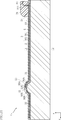
- FIG. 5 is an enlarged cross-sectional view of a main part of the cross-sectional view shown in FIG.
- FIG. 5 is an enlarged cross-sectional view of a main part obtained by enlarging a part of the cross-sectional view shown in FIG.
- FIG. 6 is an enlarged cross-sectional view of a main part of the cross-sectional view shown in FIG. It is an enlarged plan view of the main part which shows the thermal print head which concerns on 2nd Embodiment.
- FIG. 5 is a cross-sectional view taken along the line XX-XX of FIG. It is an enlarged sectional view of the main part which shows the thermal print head which concerns on the modification of 2nd Embodiment. It is sectional drawing of the main part which shows the thermal print head which concerns on 3rd Embodiment.
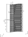
- the thermal print head A1 includes a head substrate 1, an insulating layer 19, a protective layer 2, a wiring layer 3, a resistor layer 4, a connection substrate 5, a plurality of wires 61, 62, a plurality of driver ICs 7, a protective resin 78, and a heat radiating member 8. To be equipped.
- the thermal print head A1 is incorporated in a thermal printer Pr (see FIG. 4) that prints on a print medium (not shown).
- the thermal printer Pr includes a thermal print head A1 and a platen roller 91. The platen roller 91 faces the thermal print head A1.
- the print medium is sandwiched between the thermal print head A1 and the platen roller 91, and is conveyed in the sub-scanning direction by the platen roller 91.
- Examples of such a print medium include thermal paper for producing a barcode sheet and a receipt.
- a platen made of flat rubber may be used instead of the platen roller 91. This platen includes a portion of a columnar rubber having a large radius of curvature that is arched in cross section.
- "platen” includes both a platen roller 91 and a flat platen.
- FIG. 1 is a plan view showing the thermal print head A1.
- FIG. 2 is a plan view of a main part showing the thermal print head A1.
- FIG. 3 is an enlarged plan view of a main part showing the thermal print head A1.
- FIG. 4 is a partially enlarged cross-sectional view of the thermal printer Pr including the thermal print head A1, which corresponds to a cross-sectional view taken along the line IV-IV of FIG.
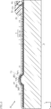
- FIG. 5 is a cross-sectional view of a main part showing the thermal print head A1.
- FIG. 6 is an enlarged cross-sectional view of a main part showing the thermal print head A1.
- the protective layer 2 is omitted.
- the protective resin 78 is omitted.
- FIG. 1 and 3 the protective resin 78 is omitted.
- FIGS. 1 to 3 the lower side in the sub-scanning direction y is the upstream side, and the upper side is the downstream side.
- FIGS. 4 to 6 the right side in the sub-scanning direction y is the upstream side, and the left side is the downstream side.
- the head substrate 1 supports the wiring layer 3 and the resistor layer 4.
- the head substrate 1 has an elongated rectangular shape with the main scanning direction x as the longitudinal direction.
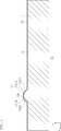
- the thickness direction of the head substrate 1 is defined as the thickness direction z.
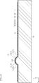
- the size of the head substrate 1 is not particularly limited, but for example, the thickness (z dimension in the thickness direction) is 725 ⁇ m, the main scanning direction x dimension is 50 mm or more and 150 mm or less, and the sub scanning direction y dimension is. It is 2.0 mm or more and 5.0 mm or less.
- the head substrate 1 is made of a single crystal semiconductor, and the single crystal semiconductor is, for example, silicon (Si).
- the head substrate 1 has a first main surface 11 and a first back surface 12, as shown in FIGS. 4 and 5.
- the first main surface 11 and the first back surface 12 are separated from each other in the thickness direction z and face each other in the thickness direction z.
- the wiring layer 3 and the resistor layer 4 are provided on the side of the first main surface 11.
- the head substrate 1 is an example of a "board", and the first main surface 11 is an example of a "main surface".
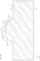
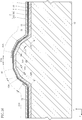
- the head substrate 1 has a convex portion 13.
- the convex portion 13 projects from the first main surface 11 in the thickness direction z and extends long in the main scanning direction x.
- the convex portion 13 is formed in the sub-scanning direction y downstream of the head substrate 1. Since the convex portion 13 is a part of the head substrate 1, it is made of Si, which is a single crystal semiconductor.
- the convex portion 13 has a top portion 130, a pair of first inclined portions 131A and 131B, and a pair of second inclined portions 132A and 132B.
- the top portion 130 is the portion of the convex portion 13 having the largest distance from the first main surface 11.
- the top 130 is, for example, a plane substantially parallel to the first main surface 11.
- the top 130 has an elongated rectangular shape that extends long in the main scanning direction x in the thickness direction z.
- the pair of first inclined portions 131A and 131B are connected to both sides of the top 130 in the sub-scanning direction y.
- the first inclined portion 131A is connected to the top portion 130 from the upstream side in the sub-scanning direction y.
- the first inclined portion 131B is connected to the top portion 130 from the downstream side in the sub-scanning direction y.
- the first inclined portion 131A is an example of the "upstream side first inclined portion”
- the first inclined portion 131B is an example of the "downstream side first inclined portion”.
- the pair of first inclined portions 131A and 131B are inclined by an angle ⁇ 1 with respect to the first main surface 11, respectively (the pair of first inclined portions 131A and 131B are inclined with respect to the first inclined angle ⁇ 1).
- Each of the pair of first inclined portions 131A and 131B is an elongated rectangular plane extending long in the main scanning direction x in the thickness direction z-view.
- the convex portion 13 may be connected to a pair of first inclined portions 131A and 131B and may have inclined portions (not shown) adjacent to the main scanning direction x both ends of the top portion 130.
- the pair of second inclined portions 132A and 132B are connected to the pair of first inclined portions 131A and 131B from the side opposite to the top 130 in the sub-scanning direction y.
- the second inclined portion 132A is sandwiched between the first inclined portion 131A and the first main surface 11 in the sub-scanning direction y.
- the second inclined portion 132A is connected to the first inclined portion 131A from the upstream side in the sub-scanning direction y, and is connected to the first main surface 11 from the downstream side in the sub-scanning direction y.
- the second inclined portion 132B is sandwiched between the first inclined portion 131B and the first main surface 11 in the sub-scanning direction y.
- the second inclined portion 132B is connected to the first inclined portion 131B from the downstream side in the sub-scanning direction y, and is connected to the first main surface 11 from the upstream side in the sub-scanning direction y.
- the second inclined portion 132A is an example of the “upstream side second inclined portion”
- the second inclined portion 132B is an example of the “downstream side second inclined portion”.
- the pair of second inclined portions 132A and 132B are inclined by an angle ⁇ 2 with respect to the first main surface 11, respectively (the pair of second inclined portions 132A and 132B are inclined with respect to the second inclined angle ⁇ 2).
- the angle ⁇ 2 is larger than the angle ⁇ 1.
- the pair of second inclined portions 132A and 132B are elongated rectangular planes extending in the main scanning direction x in the thickness direction z-view, respectively.
- the pair of second inclined portions 132A and 132B are connected to the first main surface 11, respectively.
- the convex portion 13 may be connected to a pair of second inclined portions 132A and 132B and may have an inclined portion (not shown) located at the main scanning direction x both ends of the top scanning direction x the main scanning direction x outside.
- the first main surface 11 is the (100) surface (according to the Miller index).
- the angle ⁇ 1 (see FIG. 6) of each of the first inclined portions 131A and 131B with respect to the first main surface 11 is, for example, 30.1 degrees, and each second with respect to the first main surface 11.
- the angle ⁇ 2 (see FIG. 6) of the inclined portions 132A and 132B is, for example, 54.7 degrees.
- the z dimension of the convex portion 13 in the thickness direction is, for example, 150 ⁇ m or more and 300 ⁇ m or less.
- the insulating layer 19 covers the first main surface 11 and the convex portion 13 as shown in FIGS. 5 and 6.
- the insulating layer 19 is for more reliably insulating the first main surface 11 side of the head substrate 1.
- the insulating layer 19 is made of an insulating material.
- As the insulating material for example, SiO 2 (TEOS-SiO 2 ) formed by using TEOS (tetraethyl orthosilicate) as a raw material gas is adopted. Instead of TEOS-SiO 2 , for example, SiO 2 or SiN formed by another method may be adopted.
- the thickness of the insulating layer 19 is not particularly limited, and an example thereof is, for example, 5 ⁇ m or more and 15 ⁇ m or less (preferably 5 ⁇ m or more and 10 ⁇ m or less).
- the resistor layer 4 is supported by the head substrate 1, and in the present embodiment, as shown in FIGS. 5 and 6, the resistor layer 4 is supported by the head substrate 1 via the insulating layer 19.
- the resistor layer 4 has a plurality of heat generating portions 41.
- the plurality of heat generating portions 41 locally heat the print medium by selectively energizing each of them.
- Each heat generating portion 41 is a region of the resistor layer 4 exposed from the wiring layer 3.
- the plurality of heat generating portions 41 are arranged along the main scanning direction x, and are separated from each other in the main scanning direction x.
- the shape of each heat generating portion 41 is not particularly limited, and is, for example, a rectangular shape having the sub-scanning direction y as the longitudinal direction in the thickness direction z-view.
- the resistor layer 4 is made of a material having a higher resistance than the wiring layer 3.
- the electrical resistivity of the resistor layer 4 is 10 -6 ⁇ m or more.
- the constituent material of the resistor layer 4 for example, TaN is adopted, but instead of TaN, TaSiO 2 , TiON, PolySi, Ta 2 O 5 , RuO 2 , RuTIO, TaSiN, or the like may be adopted.
- the method for forming the resistor layer 4 is not particularly limited, but the resistor layer 4 is formed by, for example, a sputtering method, a CVD method, plating, or the like, and is appropriately selected depending on the constituent material to be adopted.
- the resistor layer 4 is formed by a sputtering method.
- the thickness of the resistor layer 4 is not particularly limited, and an example thereof is 0.02 ⁇ m or more and 0.1 ⁇ m or less (preferably about 0.08 ⁇ m).
- each heat generating portion 41 is formed so as to extend from the first inclined portion 131B to the top 130.
- the sub-scanning direction y upstream end of each heat generating portion 41 is located on the top portion 130, and the sub-scanning direction y downstream end of each heat generating portion 41 is located on the first inclined portion 131B.
- the sub-scanning direction y dimension of the portion of each heat generating portion 41 formed on the top 130 is, for example, about 10% or more and 30% or less of the sub-scanning direction y dimension of the entire heat generating portion 41.
- the wiring layer 3 constitutes an energization path for energizing a plurality of heat generating portions 41.
- the wiring layer 3 is supported by the head substrate 1, and in the present embodiment, as shown in FIGS. 5 and 6, the wiring layer 3 is laminated on the resistor layer 4.
- the wiring layer 3 has a plurality of individual electrodes 31 and a common electrode 32 as shown in FIGS. 1 to 3, 5 and 6.
- each of the plurality of individual electrodes 31 has a strip shape extending substantially in the sub-scanning direction y.
- the plurality of individual electrodes 31 are arranged on the upstream side of the sub-scanning direction y with respect to the plurality of heat generating portions 41.
- the sub-scanning direction y downstream end of each individual electrode 31 is arranged at a position overlapping the top 130 on the sub-scanning direction y upstream side of the convex portion 13.
- each individual electrode 31 has an individual pad 311.
- the individual pad 311 is a portion to which the wire 61 for conducting with the driver IC 7 is connected.
- the common electrode 32 has a connecting portion 323 and a plurality of strip-shaped portions 324.
- Each of the plurality of strip-shaped portions 324 is arranged on the downstream side in the sub-scanning direction y with respect to each heat generating portion 41.
- the sub-scanning direction y upstream end of each strip-shaped portion 324 faces the sub-scanning y downstream end of each individual electrode 31 with the heat generating portion 41 interposed therebetween.
- the sub-scanning direction y upstream end of the strip-shaped portion 324 is arranged at a position overlapping the first inclined portion 131B of the convex portion 13.
- the connecting portion 323 is located on the downstream side in the sub-scanning direction y of the plurality of strip-shaped portions 324, and the plurality of strip-shaped portions 324 are connected to each other.
- the connecting portion 323 is a relatively wide portion extending in the main scanning direction x and having a sub-scanning direction y dimension larger than the main scanning direction x dimension of each strip-shaped portion 324. As shown in FIG. 1, the connecting portion 323 extends from the sub-scanning direction y downstream side of the plurality of heat generating portions 41 to the sub-scanning direction y upstream side by bypassing both sides of the main scanning direction x.
- the sub-scanning direction y downstream side portions of the plurality of strip-shaped portions 324 and the connecting portion 323 are located on the first main surface 11 of the head substrate 1 (in other words, the first main surface). It is formed (above the surface 11).
- the wiring layer 3 (plurality of individual electrodes 31 and common electrodes 32) includes a first conductor layer 301 and a second conductor layer 302 laminated in the thickness direction z.
- the first conductor layer 301 is formed on the resistor layer 4.
- the first conductor layer 301 is made of a material having a lower resistance than the resistor layer 4 and a higher resistance than the second conductor layer 302.
- the electrical conductivity of the first conductor layer 301 is, for example, 10 -6 to 10 -7 ⁇ m.
- the thermal conductivity of the first conductor layer 301 is smaller than, for example, 100 W / m.
- Ti titanium
- Ti titanium
- the method for forming the first conductor layer 301 is not particularly limited, but is formed by, for example, a sputtering method, a CVD method, plating, or the like, and is appropriately selected depending on the constituent material to be adopted.
- the constituent material of the first conductor layer 301 is Ti
- the first conductor layer 301 is formed by a sputtering method.
- the thickness of the first conductor layer 301 is not particularly limited, but an example thereof is 0.1 ⁇ m or more and 0.2 ⁇ m or less.
- the second conductor layer 302 is formed on the first conductor layer 301.
- the second conductor layer 302 partially covers the first conductor layer 301. Therefore, the first conductor layer 301 has a portion exposed from the second conductor layer 302.
- the second conductor layer 302 is made of a material having a lower resistance than the resistor layer 4 and the first conductor layer 301.
- the electrical resistivity of the second conductor layer 302 is, for example, 10 -7 ⁇ m or less.
- the second conductor layer 302 is made of a material having a higher thermal conductivity than the first conductor layer 301.
- the thermal conductivity of the second conductor layer 302 is, for example, 100 W / m or more.
- the constituent material of the second conductor layer 302 for example, Cu is adopted, but instead of Cu, Cu alloy, Al, Al alloy, Au, Ag, Ni, W (tungsten) or the like may be adopted.
- the method for forming the second conductor layer 302 is not particularly limited, but is formed by, for example, a sputtering method, a CVD method, plating, or the like, and is appropriately selected depending on the constituent material to be adopted.
- the constituent material of the second conductor layer 302 is Cu
- the second conductor layer 302 is formed by a sputtering method.
- the second conductor layer 302 When the constituent materials of the second conductor layer 302 are Au, Ag, and Ni, they are generally formed by plating, but in this case, the second conductor layer 302 includes a seed layer (for example, Cu) and the like. You may be.
- the second conductor layer 302 is thicker than the first conductor layer 301.
- the thickness of the second conductor layer 302 depends on the material used, the value of the current flowing through the wiring layer 3, and the like.
- An example of the thickness of the second conductor layer 302 is 0.5 ⁇ m or more and 5 ⁇ m or less.
- the wiring layer 3 has a pair of sub-heating portions 35A and 35B and a pair of conductive portions 36A and 36B for each of the plurality of heat-generating portions 41.
- the pair of sub-heating portions 35A and 35B are composed of portions of the first conductor layer 301 exposed from the second conductor layer 302. That is, the pair of sub-heating portions 35A and 35B are portions in the wiring layer 3 in which the second conductor layer 302 is not laminated on the first conductor layer 301.
- the pair of sub-heating portions 35A and 35B are adjacent to both ends of each of the sub-heating portions 41 in the sub-scanning direction y.
- the sub-heating unit 35A is adjacent to each heat-generating unit 41 from the upstream side in the sub-scanning direction y
- the sub-heating unit 35B is adjacent to each heat-generating unit 41 from the downstream side in the sub-scanning direction y.
- the sub-heating section 35A is an example of the "upstream sub-heating section”
- the sub-heating section 35B is an example of the "downstream sub-heating section”.
- the sub heat generating portion 35A is formed on the top 130. Both ends of the sub-scanning direction y of the sub-heating portion 35A are located on the top 130, respectively.
- the sub-heating portion 35B is formed so as to extend from the first inclined portion 131B to the second inclined portion 132B.
- the sub-scanning direction y upstream end of the sub-heating portion 35B is located on the first inclined portion 131B, and the sub-scanning direction y downstream end of the sub-heating portion 35B is located on the second inclined portion 132B.
- the pair of conductive portions 36A and 36B are composed of a first conductor layer 301 and a second conductor layer 302. That is, the pair of conductive portions 36A and 36B are portions in the wiring layer 3 in which the second conductor layer 302 is laminated on the first conductor layer 301.
- the pair of conductive portions 36A and 36B are located on the opposite side of the pair of sub-heating portions 35A and 35B in the sub-scanning direction y from each of the sub-heating portions 41.
- the conductive portion 36A is adjacent to the sub-heating portion 35A from the upstream side in the sub-scanning direction y
- the conductive portion 36B is adjacent to the sub-heating portion 35B from the downstream side in the sub-scanning direction y.
- the conductive portion 36A is an example of the “upstream conductive portion”
- the conductive portion 36B is an example of the “downstream conductive portion”.
- the conductive portion 36A is formed from the top portion 130 via the first inclined portion 131A and the second inclined portion 132A so as to straddle the first main surface 11 on the side upstream of the convex portion 13 in the sub-scanning direction y.
- the sub-scanning direction y downstream end of the conductive portion 36A is located on the top 130.
- the conductive portion 36B is formed so as to extend from the second inclined portion 132B to the first main surface 11 on the side downstream of the convex portion 13 in the sub-scanning direction y.
- the sub-scanning direction y upstream end of the conductive portion 36B is located on the second inclined portion 132B.
- each of the conductive portions 36A and 36B has a resistance value per unit length in the sub-scanning direction y. It is smaller than each heat generating portion 41. Further, in each of the sub-heating units 35A and 35B, the resistance value per unit length in the sub-scanning direction y is between the heat-generating portion 41 and the conductive portions 36A and 36B.
- the heat generating portions 41 when the heat generating portions 41 are energized, the amount of heat generated by each of the pair of sub heat generating parts 35A and 35B is smaller than the amount of heat generated by each of the heat generating parts 41, and the pair of conductive parts 36A and 36B It is larger than the calorific value in each.
- the pair of sub heat generating portions 35A and 35B are each about 150 to 200 ° C.
- the protective layer 2 covers the wiring layer 3 and the resistor layer 4, and protects the wiring layer 3 and the resistor layer 4.
- the protective layer 2 is made of an insulating material.
- As the insulating material for example, SiN (silicon nitride) is adopted, but SiO 2 (silicon oxide), SiC (silicon carbide), AlN (aluminum nitride) and the like may be adopted instead of SiN.
- the protective layer 2 is composed of a single layer or a plurality of layers including the above-mentioned insulating material.
- the thickness of the protective layer 2 is not particularly limited, but an example thereof is 1.0 ⁇ m or more and 10 ⁇ m or less.
- the protective layer 2 has a plurality of pad openings 21.
- Each pad opening 21 penetrates the protective layer 2 in the thickness direction z.
- Each of the plurality of pad openings 21 exposes the individual pads 311 of the individual electrodes 31.
- the plurality of pad openings 21 may be filled with a conductive material.
- a plating layer may be formed on the conductive material.
- the structure of this plating layer is not particularly limited, but for example, Ni, Pd (palladium), and Au are laminated in this order from the surface of the conductive material.
- connection board 5 is arranged on the side upstream of the sub-scanning direction y with respect to the head board 1.
- the connection board 5 is, for example, a PCB board on which a driver IC 7 and a connector 59 described later are mounted.
- the shape of the connecting substrate 5 is not particularly limited, but in the present embodiment, it is a rectangular shape having the main scanning direction x as the longitudinal direction.
- the connection board 5 has a second main surface 51 and a second back surface 52.
- the second main surface 51 is a surface facing the same side as the first main surface 11 of the head substrate 1
- the second back surface 52 is a surface facing the same side as the first back surface 12 of the head substrate 1.
- the second main surface 51 is located below the first main surface 11 in the thickness direction z figure.
- the driver IC 7 is mounted on the second main surface 51 of the connection board 5, and is for individually energizing a plurality of heat generating portions 41.
- the plurality of driver ICs 7 are connected to the plurality of individual electrodes 31 by the plurality of wires 61.
- the energization control of the plurality of heat generating units 41 by the plurality of driver ICs 7 follows a command signal input from outside the thermal print head A1 via the connection board 5.
- the plurality of driver ICs 7 are connected to the wiring pattern (not shown) of the connection board 5 by the plurality of wires 62.
- the plurality of driver ICs 7 are appropriately provided according to the number of the plurality of heat generating portions 41.
- the plurality of driver ICs 7, the plurality of wires 61, and the plurality of wires 62 are covered with the protective resin 78.
- the protective resin 78 is made of, for example, an insulating resin and is, for example, black.
- the protective resin 78 is formed so as to straddle the head substrate 1 and the connection substrate 5.
- the connector 59 is used to connect the thermal print head A1 to the thermal printer Pr.
- the connector 59 is attached to the connection board 5 and is connected to the wiring pattern (not shown) of the connection board 5.
- the heat radiating member 8 supports the head substrate 1 and the connecting substrate 5, and is for radiating a part of the heat generated by the plurality of heat generating portions 41 to the outside through the head substrate 1.
- the heat radiating member 8 is a block-shaped member made of a metal such as Al.
- the heat radiating member 8 has a first support surface 81 and a second support surface 82.
- the first support surface 81 and the second support surface 82 each face upward in the thickness direction z, and are arranged side by side in the sub-scanning direction y.
- the first back surface 12 of the head substrate 1 is joined to the first support surface 81.
- the second back surface 52 of the connection board 5 is joined to the second support surface 82.
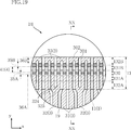
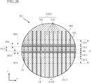
- a substrate material 1K is prepared.
- the substrate material 1K is made of a single crystal semiconductor and is, for example, a part of a substantially circular Si wafer.
- One Si wafer contains a plurality of substrate materials 1K.
- one substrate material 1K (head substrate 1) which is a part of a Si wafer and corresponds to one thermal print head A1 may be illustrated.
- the thickness of the substrate material 1K (in other words, the thickness of the Si wafer) is not particularly limited, but in the present embodiment, it is, for example, about 725 ⁇ m.
- the substrate material 1K has a first main surface 11K and a first back surface 12K facing opposite sides.
- the first main surface 11K is the (100) surface.
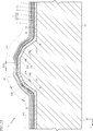
- a convex portion 13K is formed on the substrate material 1K.
- the convex portion 13K protrudes from the first main surface 11K and extends long in the main scanning direction x.
- the convex portion 13K has a top portion 130K and a pair of inclined portions 132K.
- the top 130K is a plane parallel to the first main surface 11K and is the same (100) plane as the first main surface 11K.
- the pair of inclined portions 132K are located on both sides of the top portion 130K in the sub-scanning direction y, and are interposed between the top portion 130K and the first main surface 11K.
- the pair of inclined portions 132K are planes inclined with respect to the top portion 130K and the first main surface 11K, respectively.
- the angle formed by each of the pair of inclined portions 132K and the first main surface 11K and the top portion 130K is 54.7 degrees.
- the convex portion 13 has a top portion 130, a pair of first inclined portions 131A and 131B, and a pair of second inclined portions 132A and 132B.
- the top portion 130 is a portion that was the top portion 130K
- the pair of second inclined portions 132A and 132B are portions that were the pair of inclined portions 132K.
- the pair of first inclined portions 131A and 131B is a portion where the boundary between the top portion 130K and the pair of inclined portions 132K is etched by KOH.
- the angle ⁇ 1 (see FIG. 10) of each of the first inclined portions 131A and 131B with respect to the first main surface 11 is 30.1 degrees
- the angle ⁇ 2 of each of the second inclined portions 132A and 132B with respect to the first main surface 11 is 54.7 degrees.
- the step of forming the head substrate 1 from the substrate material 1K described above is an example of the “board processing step”. In the substrate processing step, the first main surface 11 and the convex portion 13 are formed.
- the insulating layer 19 is formed.
- the insulating layer 19 is formed by depositing SiO 2 formed using TEOS (tetraethyl orthosilicate) as a raw material gas on the head substrate 1 using, for example, CVD.
- TEOS tetraethyl orthosilicate
- the method for forming the insulating layer 19 is not limited to this, and other methods may be used.
- a resistor film 4K is formed.
- a thin film of TaN is formed on the insulating layer 19 by sputtering.
- the method for forming the resistor film 4K is not limited to this, and other methods may be used.
- a wiring film 3K is formed.
- the step of forming the wiring film 3K there are two steps of forming the first conductor film 301K shown in FIG. 13 and forming the second conductor film 302K shown in FIG.
- first film forming step for example, a thin film of Ti is formed on the resistor film 4K by sputtering. At this time, the first conductor film 301K covers substantially the entire surface of the resistor film 4K.
- the second conductor film 302K In the step of forming the second conductor film 302K (second film forming step), for example, a layer made of Cu is formed on the first conductor film 301K by plating, sputtering, or the like. At this time, the second conductor film 302K covers substantially the entire surface of the first conductor film 301K.
- partial removal of the second conductor film 302K, partial removal of the first conductor film 301K, and partial removal of the resistor film 4K are performed in this order.
- a step of partially removing the first conductor film 301K (first partial removal step), a step of partially removing the second conductor film 302K (second partial removal step), and a step of partially removing the resistor film 4K.
- Each step (resistive film partial removal step) is performed by, for example, etching.
- the first conductor layer 301 is formed by the first partial removal step
- the second conductor layer 302 is formed by the second partial removal step
- the resistor layer 4 is formed by the resistor film partial removal step.
- the step of forming the wiring layer 3 includes a first film forming step, a second film forming step, a first partial removing step, and a second partial removing step.
- the step of forming the resistor layer 4 includes a resistor film forming step and a resistor film partial removing step.
- the resistor film partial removal step may be performed before the first film forming step and the second film forming step.
- the formed first conductor layer 301 and second conductor layer 302 constitute the wiring layer 3, and the wiring layer 3 has a plurality of individual electrodes 31 and a common electrode 32. Further, the wiring layer 3 has a plurality of sub-heating portions 35A and 35B and a plurality of conductive portions 36A and 36B.
- the formed resistor layer 4 has a plurality of heat generating portions 41.
- the protective layer 2 is formed.
- the formation of the protective layer 2 is carried out by depositing SiN on the insulating layer 19, the wiring layer 3 (the first conductor layer 301 and the second conductor layer 302) and the resistor layer 4, for example, by using CVD. Further, the pad opening 21 is formed by partially removing the protective layer 2 by etching or the like. After that, one Si wafer is separated into a plurality of head substrates 1 (see FIGS. 1, 4 and 5) by using a dicing device or the like.
- the assembly process is performed on one head substrate 1.
- the process includes steps such as attaching the head substrate 1 and the connecting substrate 5 to the heat radiating member 8, mounting the driver IC 7 on the connecting substrate 5, bonding the plurality of wires 61 and the plurality of wires 62, and forming the protective resin 78.
- the above-mentioned thermal print head A1 is obtained.
- thermal print head A1 The actions and effects of the above-mentioned thermal print head A1 are as follows.
- the sub heat generating portions 35A and 35B are sandwiched between the heat generating portions 41 and the conductive portions 36A and 36B in the sub scanning direction y.
- the sub heat generating portions 35A and 35B are lower than the heat generating portions 41 and have a higher temperature than the conductive portions 36A and 36B.
- the temperature gradient in the sub-scanning direction y can be relaxed as compared with the case where the heat generating portions 41 and the conductive portions 36A and 36B are adjacent to each other. If the heat generating portions 41 and the conductive portions 36A and 36B are adjacent to each other, the thermal stress generated by the temperature difference between them may cause disconnection, for example, at the boundary portion between them.
- the thermal print head A1 can suppress damage caused by thermal stress, and can improve the durability and reliability of the thermal print head A1.
- a pair of sub-heating portions 35A and 35B are provided on both sides of the sub-scanning direction y of each heat-generating portion 41 in order to improve durability and reliability by relaxing the temperature gradient.
- a sub-heating unit 35A is provided on the upstream side in the sub-scanning direction y of each heat-generating unit 41.
- the print medium sent in the sub-scanning direction y is heated by the sub-heating unit 35A and then heated by each of the heat-generating units 41 having a higher temperature.
- the sub heat generating portion 35A generates heat at a temperature higher than that of the conductive portion 36A, for example, it is about 150 to 200 ° C. under energization conditions where each heat generating portion 41 is about 300 ° C.
- the print medium which is a heat-sensitive paper having general sensitivity is sub. No clear color is produced by heating by the heat generating portion 35A.
- color development occurs more quickly and clearly because it was preheated by the sub-heating section 35A. Therefore, it is possible to improve the print quality and the print speed. Further, as compared with the case where the sub heat generating portion 35A is not provided, it is possible to develop the color of the print medium even if the temperature of each heat generating portion 41 is lowered.
- the thermal print head A1 can save energy and extend its life.
- the first conductor layer 301 is made of a material having a lower thermal conductivity than the second conductor layer 302. As a result, it is possible to prevent the sub heat generating portion 35A from releasing the heat generated in the heat generating portion 41 to the conductive portion 36A side. Therefore, since the heat generated in the heat generating unit 41 is suppressed from being unnecessarily released, energy efficiency and heat generation responsiveness can be improved.
- the convex portion 13 has a top portion 130, a pair of first inclined portions 131A and 131B, and a pair of second inclined portions 132A and 132B, and a pair of first inclined portions sandwiching the top portion 130.
- the 131A and 131B and the pair of second inclined portions 132A and 132B are arranged in the sub-scanning direction y. Therefore, the convex portion 13 has a configuration that is inclined in two stages with respect to the top portion 130 (first main surface 11). Therefore, it is possible to reduce the angle ⁇ 1 formed by the top portion 130 and the first inclined portions 131A and 131B, which is preferable for improving the print quality.
- each heat generating portion 41 is formed on the first inclined portion 131B.
- good print quality can be obtained even when the contact center 910 (see FIG. 4) of the platen roller 91 with respect to each heat generating portion 41 is biased toward the downstream side in the sub-scanning direction y with respect to the convex portion 13.
- Such an arrangement is advantageous in avoiding interference between the platen roller 91 and the protective resin 78, and the sub-scanning direction y of the head substrate 1 can be reduced.
- each heat generating portion 41 is formed so as to extend from the first inclined portion 131B to the top 130. As a result, even if the platen roller 91 is displaced in the sub-scanning direction y, deterioration of print quality can be suppressed.
- the sub heat generating portion 35A is formed on the top 130, and is not formed on the first inclined portion 131A.
- the sub heat generating portion 35 is formed so as to extend from the top portion 130 to the first inclined portion 131A in consideration of the positional deviation of the platen roller 91 in the sub scanning direction y.
- the contact center 910 is hardly displaced to the upstream side in the sub-scanning direction y from the top 130.
- the sub-heating portion 35A does not contribute significantly to printing, and the larger the sub-heating portion 35A, the greater the energy loss. From these facts, the thermal print head A1 suppresses energy loss as compared with the case where the sub heat generating portion 35A is formed so as to straddle the top 130 to the first inclined portion 131A, and the printing efficiency due to the energy loss is improved. The decrease can be suppressed. That is, the thermal print head A1 can suppress a decrease in printing efficiency due to energy loss by adjusting the size (formation region) of the sub-heating portion 35A while relaxing the temperature gradient by providing the sub-heating portion 35A. ..
- the common electrode 32 is located on the sub-scanning direction y downstream side with respect to the plurality of heat generating portions 41, a plurality of individual electrodes 32 are located on the sub-scanning direction y upstream side of the plurality of heat generating portions 41. Only the electrodes 31 are arranged. As a result, the arrangement pitch of the plurality of individual electrodes 31 in the main scanning direction x can be reduced, and high-definition printing can be achieved.
- the constituent material of the first conductor layer 301 is, for example, Ti
- the constituent material of the second conductor layer 302 is, for example, Cu.
- the resistance value per unit length in the sub-scanning direction y of the portion of the first conductor layer 301 exposed from the second conductor layer 302, that is, the sub-heating portions 35A and 35B is set to the first conductor layer 301. It can be made larger than the resistance value per unit length in the sub-scanning direction y of the portion where the second conductor layer 302 and the second conductor layer 302 are laminated, that is, the conductive portions 36A and 36B.
- the cross-sectional areas of the sub-heat generating portions 35A and 35B in the wiring layer 3 are smaller than the cross-sectional areas of the conductive portions 36A and 36B.
- the resistance value of each of the sub-heating portions 35A and 35B per unit length in the sub-scanning direction y can be made larger than the resistance value of each of the conductive portions 36A and 36B per unit length in the sub-scanning direction y. ..
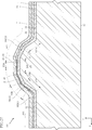
- FIG. 17 is a partially enlarged cross-sectional view of the thermal printer Pr including the thermal print head B1 and corresponds to the cross-sectional view of FIG. 4 in the first embodiment.
- FIG. 18 is a cross-sectional view of a main part showing the thermal print head B1 and corresponds to the cross-sectional view of FIG. 5 in the first embodiment.
- FIG. 19 is an enlarged plan view of a main part showing the thermal print head B1.
- FIG. 20 is an enlarged cross-sectional view of a main part along the line XX-XX of FIG.
- the convex portion 13 is formed so as to be in contact with the end on the downstream side in the sub-scanning direction y of the head substrate 1. That is, the first main surface 11 does not exist in the region on the downstream side of the sub-scanning direction y from the convex portion 13. Therefore, in the wiring layer 3 of the present embodiment, as shown in FIG. 20, the end of the conductive portion 36B on the downstream side in the sub-scanning direction y overlaps with the second inclined portion 132B.
- the wiring layer 3 of the present embodiment has a plurality of individual electrodes 31, a plurality of common electrodes 32, and a plurality of relay electrodes 33.
- the plurality of individual electrodes 31 and the plurality of common electrodes 32 are arranged on the side upstream of the sub-scanning direction y with respect to the plurality of heat generating portions 41.
- the plurality of relay electrodes 33 are arranged on the side downstream of the sub-scanning direction y with respect to the plurality of heat generating portions 41.
- the plurality of individual electrodes 31 and the plurality of common electrodes 32 are arranged substantially in parallel at a predetermined pitch in the main scanning direction x.
- the plurality of relay electrodes 33 are arranged at a predetermined pitch in the main scanning direction x.
- Each relay electrode 33 has a shape that constitutes an energization path that folds back in the sub-scanning direction y.
- Each relay electrode 33 is formed so as to extend from the first inclined portion 131B to the second inclined portion 132B of the convex portion 13.
- the common electrode 32 on the left side of the two common electrodes 32 assigned by the reference numeral “32 (3)” in FIG. 19 will be described as an example.
- the common electrode 32 has a branch portion 325 and two adjacent strip-shaped portions 324.
- the two strip-shaped portions 324 are located at the downstream end in the sub-scanning direction y in each common electrode 32.
- the branch portion 325 is provided on the downstream side in the sub-scanning direction y in each common electrode 32, and is connected to the two strip-shaped portions 324.
- the branch portion 325 is connected to two adjacent heat generating portions 41 (fourth and fifth from the left in FIG.
- the heat generating portion 41 (third and sixth from the left) is arranged. Then, the two heat generating portions 41 located outside the main scanning direction x the two adjacent heat generating portions 41 have two individual electrodes 31 (two individual electrodes located on both sides of the representative common electrode 32). Electrodes 31) are adjacent to each other.
- two adjacent energization paths are configured from one common electrode 32.
- Each of the two energization paths is connected in the order of connection, one common electrode 32, one branch portion 325, one strip-shaped portion 324 of two strip-shaped portions 324, one heat generating portion 41, and one relay electrode 33. It has another heating unit 41 adjacent to the one heating unit 41 described above and one individual electrode 31.
- the two heat generating portions 41 connected between the one individual electrode 31 and the common electrode 32 and adjacent to each other in the main scanning direction x are energized to generate heat. be able to.
- These two adjacent heat generating portions 41 correspond to one point (1 dot) on the print medium.
- the contact center 910 between the platen roller 91 and each heat generating portion 41 is arranged to be located on the sub-scanning direction y downstream side with respect to the convex portion 13 of the head substrate 1.
- the platen roller 91 is pressed against the plurality of heat generating portions 41 formed on the convex portions 13 via the protective layer 2 in a posture biased toward the downstream side in the sub-scanning direction y.
- each sub-heating portion 35A and 35B is sandwiched between each heating portion 41 and each conductive portion 36A and 36B.
- the temperature gradient in the sub-scanning direction y can be relaxed as compared with the case where the heat generating portions 41 and the conductive portions 36A and 36B are adjacent to each other. Therefore, the durability and reliability of the thermal print head B1 can be improved as in the first embodiment.
- the first main surface 11 does not exist in the region on the downstream side of the sub-scanning direction y from the convex portion 13. According to this configuration, the sub-scanning direction y downstream side of the head substrate 1 can be shortened. Therefore, when the print medium is conveyed, it is possible to prevent the print medium from coming into contact with the head substrate 1 on the side downstream of the convex portion 13 in the sub-scanning direction y.
- This is preferable in order to make the thermal printer Pr incorporating the thermal print head B1 a straight pass mechanism because the print medium P1 can be conveyed without being bent or bent as shown in FIG.
- a plastic card having a heat-sensitive layer or the like can be used as a printing medium.
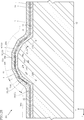
- FIG. 21 is an enlarged cross-sectional view of a main part showing the thermal print head B2 according to such a modification, and corresponds to the cross-sectional view of FIG.
- the thermal print head B2 Since the first main surface 11 of the thermal print head B2 on the sub-scanning direction y downstream side of the convex portion 13 is extremely small, as with the thermal print head B1, when the print medium is conveyed, the thermal print head B2 is more than the convex portion 13. It is also possible to prevent the print medium from coming into contact with the head substrate 1 on the downstream side in the sub-scanning direction y. That is, the thermal print head B2 shown in FIG. 21 is also preferable in terms of forming a straight pass mechanism, like the thermal print head B1.
- FIG. 22 and 23 show the thermal print head C1 according to the third embodiment.
- FIG. 22 is a cross-sectional view of a main part showing the thermal print head C1 and corresponds to FIG.
- FIG. 23 is an enlarged cross-sectional view of a main part showing the thermal print head C1 and corresponds to FIG.
- the thermal print head C1 has a different stacking order of the resistor layer 4 and the wiring layer 3 from the thermal print head A1.
- the wiring layer 3 first conductor layer 301 and second conductor layer 302 is laminated on the head substrate 1 (first main surface 11 and convex portion 13) via the insulating layer 19.
- a resistor layer 4 is formed on the resistor layer 4.
- the resistor layer 4 is formed after the wiring layer 3 is formed.
- the resistor film forming step is not performed, and the first film forming step and the second film forming step are performed. Do it in order.
- the first partial removal step and the second partial removal step are performed.
- the wiring layer 3 (first conductor layer 301 and second conductor layer 302) is laminated on the insulating layer 19. That is, the wiring layer forming step is performed before the resistor film forming step.
- the resistor film forming step and the resistor film partial removing step are performed in this order.
- the resistor layer 4 is laminated on the wiring layer 3 and the insulating layer 19 exposed from the wiring layer 3.
- the processing after the formation of the protective layer 2 is performed as in the case of the thermal print head A1.
- each sub-heating portion 35A and 35B is sandwiched between each heating portion 41 and each conductive portion 36A and 36B.
- the temperature gradient in the sub-scanning direction y can be relaxed as compared with the case where the heat generating portions 41 and the conductive portions 36A and 36B are adjacent to each other. Therefore, the durability and reliability of the thermal print head C1 can be improved as in the first embodiment.
- the wiring layer 3 (first conductor layer 301 and second conductor layer 302) and the resistor layer 4 are laminated in this order on the insulating layer 19. That is, in the method for manufacturing the thermal print head C1, the wiring layer 3 is formed on the insulating layer 19, and then the resistor layer 4 is formed.
- the resistor film 4K, the first conductor film 301K, and the second conductor film 302K are formed in this order, and then each of the first conductor film 301K and the second conductor film 302K, for example, is formed. It is partially removed by etching.
- the resistor film 4K, the first conductor film 301K, and the second conductor film 302K are formed and then etched in sequence, the transfer between the film forming apparatus and the etching apparatus becomes unnecessary, and the conveying work can be reduced.
- the resistor film 4K is also exposed to this etching. Therefore, the resistor film 4K may be damaged depending on the material of the resistor film 4K and the etching methods of the first conductor film 301K and the second conductor film 302K.
- a resistor film 4K (resistor layer 4) is formed after processing the first conductor layer 301 and the second conductor layer 302 (first partial removal step and second partial removal step). Therefore, the resistor film 4K is not damaged. That is, it is possible to reduce the application of processing damage to the resistor layer 4 (each heat generating portion 41).
- the stacking order of the first conductor layer 301 and the second conductor layer 302 is not limited to the above example and may be reversed.
- 24 and 25 show the thermal printhead C2 according to such a modification.
- FIG. 24 is a cross-sectional view of a main part showing the thermal print head C2, which corresponds to FIG. 22.
- FIG. 25 is an enlarged cross-sectional view of a main part showing the thermal print head C2, and corresponds to FIG. 23.
- the wiring layer 3 is laminated on the insulating layer 19 in the order of the second conductor layer 302 and the first conductor layer 301, and the resistor layer 4 is formed. It is laminated on the first conductor layer 301.
- the sub-heat generating portions 35A and 35B are formed by the portion of the first conductor layer 301 that is not formed on the second conductor layer 302, that is, the portion of the first conductor layer 301 that is in contact with the insulating layer 19. Is configured.
- the thermal print head C2 can also have the same effect as the thermal print head C1.
- the resistor layer 4 is interposed between the individual pads 311 and the wiring layer 3, but the size of the individual pads 311 in a plan view is large.
- the thinness of the resistor layer 4 does not significantly affect the continuity between the individual pads 311 and the wiring layer 3. In order to improve the continuity between the individual pads 311 and the wiring layer 3, it is desirable not to provide the resistor layer 4 between them.
- the thermal print heads C1 and C2 even if the first main surface 11 does not exist in the region on the side downstream of the convex portion 13 in the sub-scanning direction y.
- a very small amount of the first main surface 11 may be present.
- FIG. 26 and 27 show the thermal print head D1 according to the fourth embodiment.
- FIG. 26 is an enlarged plan view of a main part showing the thermal print head D1 and corresponds to FIG. 3 in the first embodiment.
- FIG. 27 is an enlarged cross-sectional view of a main part showing the thermal print head D1 and corresponds to FIG. 6 in the first embodiment.
- the thermal print head D1 has a different formation range of the resistor layer 4 and the first conductor layer 301 from the thermal print head A1.
- the resistor layer 4 is formed so as to extend from the top 130 to the first inclined portion 131B, and the first inclined portion 131A, the pair of second inclined portions 132A, 132B and It is not formed on the first main surface 11.
- a part of the first conductor layer 301 is formed on the resistor layer 4, and the other part is directly formed on the insulating layer 19.
- the first conductor layer 301 may be formed on the top 130 or may be formed so as to extend from the first inclined portion 131B to the second inclined portion 132B.
- a part of the second conductor layer 302 is formed on the first conductor layer 301, and the other part is directly formed on the insulating layer 19.
- the second conductor layer 302 is formed so as to straddle the first main surface 11 from the top 130 via the first inclined portion 131A and the second inclined portion 132A, and the second inclined portion 132B to the first main surface 11 Some are formed across.
- the wiring layer 3 (first conductor layer 301 and the second conductor layer 302) and the resistor layer 4 are formed, and these are locally compared with the thermal print head A1. It is formed.
- the sub-heating portions 35A and 35B are configured by the portion of the first conductor layer 301 exposed from the second conductor layer 302, that is, the portion that does not overlap the second conductor layer 302 in the z-direction view. Further, the conductive portions 36A and 36B are formed by the portions where the second conductor layer 302 is formed.
- the resistor film forming step, the resistor film partial removing step, the first film forming step, the first partial removing step, the second film forming step, and the second partial removing step are processed in this order.
- the resistor layer 4 and the wiring layer 3 are formed in order. That is, the wiring layer forming step is performed after the resistor layer forming step.
- the resistor layer 4 and the first conductor layer 301 are locally formed as compared with the thermal print head A1.
- the thermal print head D1 similarly to the thermal print head A1, the sub-heating portions 35A and 35B are sandwiched between the heat-generating portions 41 and the conductive portions 36A and 36B. As a result, the temperature gradient in the sub-scanning direction y can be relaxed as compared with the case where the heat generating portions 41 and the conductive portions 36A and 36B are adjacent to each other. Therefore, the durability and reliability of the thermal print head D1 can be improved as in the first embodiment.
- the resistor layer 4 and the first conductor layer 301 are locally arranged as compared with the thermal print head A1.
- the thermal print head D1 can easily adjust the formation positions and sizes of the heat generating portions 41, the sub heat generating portions 35A and 35B, and the conductive portions 36A and 36B, respectively, and the material cost is lower than that of the thermal print head A1. can.
- the resistor layer 4 and the first conductor layer 301 are locally arranged in the thermal print head A1
- the present invention is not limited to this.
- the resistor layer 4 and the first conductor layer 301 may be locally arranged in each of the thermal print heads C1 and C2.
- FIG. 28 shows a case where the resistor layer 4 and the first conductor layer 301 are locally arranged in the thermal print head C1, and is an enlarged cross-sectional view of a main part showing the thermal print head D2 according to the modified example.
- FIG. 29 shows a case where the resistor layer 4 and the first conductor layer 301 are locally arranged in the thermal print head C2, and is an enlarged cross-sectional view of a main part showing the thermal print head D3 according to the modified example. ..
- the resistor layer 4 and the first conductor layer 301 are locally arranged as shown in FIGS. 28 and 29. Therefore, as with the thermal print head D1, it is easy to adjust the formation positions and sizes of the heat generating portions 41, the sub heat generating portions 35A and 35B, and the conductive portions 36A and 36B, and the material cost is higher than that of the thermal print head A1. Can be cheaper.
- the resistor layer forming step is performed after the wiring layer forming step (that is, after the first partial removing step and the second partial removing step, the resistor film is formed. (Because the forming step is performed), it is possible to reduce the processing damage to the resistor layer 4 in the same manner as in the thermal printheads C1 and C2 (see FIGS. 22 to 25) according to the third embodiment and its modification. can.
- FIG. 30 shows a case where the thermal print head D1 has a very small amount of the first main surface 11 as in the modified example of the second embodiment.
- FIG. 30 is an enlarged cross-sectional view of a main part showing the thermal print head according to the modified example.
- FIG. 31 and 32 show the thermal print head E1 according to the fifth embodiment.
- FIG. 31 is an enlarged cross-sectional view of a main part showing the thermal print head E1 and corresponds to FIG. 6 in the first embodiment.
- FIG. 32 is an enlarged plan view of a main part showing the thermal print head E1 and corresponds to FIG. 3 in the first embodiment.
- the thermal print head E1 has a different wiring layer 3 configuration from the thermal print head A1.
- the wiring layer 3 of the thermal print head E1 is composed of one conductor layer 300.
- the conductor layer 300 may be formed instead of the first conductor layer 301 and the second conductor layer 302.
- the conductor layer 300 is made of Cu, like the second conductor layer 302, for example. As shown in FIG. 31, the conductor layer 300 includes a thick portion 300a and a thin portion 300b having relatively different thicknesses. The thick portion 300a is formed thicker than the thin portion 300b. Since the thin-walled portion 300b has a smaller cross-sectional area than the thick-walled portion 300a, the resistance value per unit length of the thin-walled portion 300b in the sub-scanning direction y is the unit length of the thick-walled portion 300a in the sub-scanning direction y. Greater than resistance.
- each of the sub-heating portions 35A and 35B is composed of a thin-walled portion 300b
- each of the conductive portions 36A and 36B is composed of a thick-walled portion 300a.
- the thickness of each of the thick portion 300a and the thin portion 300b is not particularly limited, but the resistance value per unit length in the sub-scanning direction y is configured to have the above-mentioned relationship.
- each sub-heating portion 35A and 35B is sandwiched between each heating portion 41 and each conductive portion 36A and 36B.
- the temperature gradient in the sub-scanning direction y can be relaxed as compared with the case where the heat generating portions 41 and the conductive portions 36A and 36B are adjacent to each other. Therefore, the durability and reliability of the thermal print head E1 can be improved as in the first embodiment.
- FIG. 33 is an enlarged plan view of a main part showing the thermal print head E2 according to such a modification, and corresponds to FIG. 32.
- the thin portion 300b is patterned in a comb-teeth shape in the z-view in the thickness direction.
- the shape of the patterned thin-walled portion 300b is not limited to the comb-teeth shape shown in FIG. 33.
- each of the sub-heating portions 35A and 35B has been patterned while reducing the thickness of the conductor layer 300 (that is, providing the thin-walled portion 300b). Not limited to. For example, only patterning may be performed while keeping the thickness of the conductor layer 300 uniform (that is, without providing the thin portion 300b).
- the method for manufacturing a thermal print head, a thermal printer, and a thermal print head according to the present disclosure is not limited to the above-described embodiment.
- the specific configuration of each part of the thermal print head and the thermal printer of the present disclosure and the specific processing of each step of the method of manufacturing the thermal print head of the present disclosure can be variously redesigned.
- the disclosure includes embodiments described in the appendix below. Appendix 1.
- a substrate made of a single crystal semiconductor and having a main surface facing one side in the thickness direction,
- the wiring layer has a conductive portion whose resistance value per unit length in the sub-scanning direction is smaller than that of the heat-generating portion and a resistance value per unit length in the sub-scanning direction for each of the plurality of heat generating portions.
- the substrate has a convex portion that protrudes from the main surface and extends in the main scanning direction.
- the heat generating portion, the sub heat generating portion, and the conductive portion are formed on the convex portion.
- the sub-heating portion is a thermal print head sandwiched between the heat-generating portion and the conductive portion in the sub-scanning direction. Appendix 2.
- the convex portion has a top portion having the largest distance from the main surface, a first inclined portion on the upstream side connecting from the upstream side in the sub-scanning direction to the top portion, and a downstream side connecting from the downstream side in the sub-scanning direction to the top portion. Including 1 inclined part
- the upstream side first inclined portion and the downstream side first inclined portion are each inclined with respect to the main surface with a first inclination angle.
- the thermal print head according to Appendix 1, wherein the heat generating portion is formed so as to extend from the first inclined portion on the downstream side to the top portion. Appendix 3.
- the convex portion includes a second inclined portion on the upstream side connected to the side opposite to the top in the sub-scanning direction with respect to the first inclined portion on the upstream side, and the convex portion in the sub-scanning direction with respect to the first inclined portion on the downstream side. Includes a second slope on the downstream side that connects to the opposite side of the top, The upstream side second inclined portion and the downstream side second inclined portion are each inclined with respect to the main surface with a second inclination angle.
- the sub-heating portion includes an upstream-side sub-heating portion located on the upstream side in the sub-scanning direction and a downstream-side sub-heating portion located on the downstream side in the sub-scanning direction with reference to the heat-generating portion.
- the conductive portion includes an upstream conductive portion adjacent to the upstream sub-heating portion in the sub-scanning direction opposite to the heat-generating portion, and the heat-generating portion in the sub-scanning direction with respect to the downstream sub-heating portion.
- the thermal printhead according to Appendix 4 which includes a downstream conductive portion adjacent to the opposite side. Appendix 6.
- Appendix 7 The thermal print head according to Appendix 6, wherein the upstream conductive portion is formed so as to straddle the main surface from the top via the upstream first inclined portion and the upstream second inclined portion.
- Appendix 8 The thermal print head according to any one of Supplementary note 5 to Supplementary note 7, wherein the downstream side sub-heating portion is formed so as to extend from the downstream side second inclined portion to the downstream side first inclined portion.
- Appendix 9. The thermal print head according to Appendix 8, wherein the downstream conductive portion is formed on the downstream second inclined portion.
- each of the plurality of heat generating portions is composed of a portion of the resistor layer that does not overlap with the wiring layer when viewed in the thickness direction.
- the wiring layer includes a first conductor layer and a second conductor layer laminated in the thickness direction.
- the conductive portion is composed of a portion on which the second conductor layer is formed.
- the thermal print head according to Appendix 10, wherein the sub-heating portion is composed of a portion of the first conductor layer that does not overlap with the second conductor layer when viewed in the thickness direction.
- Appendix 12 The resistor layer is formed on the substrate and The first conductor layer is formed on the resistor layer while exposing a part of the resistor layer.
- Appendix 13 The first conductor layer is formed on the substrate and is formed on the substrate.
- the second conductor layer is formed on the first conductor layer while exposing a part of the first conductor layer.
- Appendix 14 The thermal print head according to any one of Appendix 11 to Appendix 13, wherein the first conductor layer is thinner than the second conductor layer. Appendix 15.
- the wiring layer includes a thick portion and a thin portion having relatively different dimensions in the thickness direction.
- the sub-heating portion is composed of the thin-walled portion.
- the thermal print head according to Appendix 10 wherein the conductive portion is composed of the thick portion.
- Appendix 17 The thermal print head according to Appendix 16, wherein the thin portion is patterned when viewed in the thickness direction.
- the thermal printhead according to any one of Supplementary note 1 to Supplementary note 17, wherein the single crystal semiconductor is Si. Appendix 19.
- the thermal print head according to any one of Appendix 1 to Appendix 18, A thermal printer comprising a platen facing the thermal printhead.
- Appendix 20 A substrate preparation process for preparing a substrate made of a single crystal semiconductor, A substrate processing step of forming a main surface facing one side in the thickness direction and a convex portion protruding from the main surface and extending in the main scanning direction on the substrate.
- the wiring layer has a conductive portion whose resistance value per unit length in the sub-scanning direction is smaller than that of the heat-generating portion and a resistance value per unit length in the sub-scanning direction for each of the plurality of heat generating portions. Includes a sub-heating portion that sandwiches between the heat-generating portion and the conductive portion.
- the heat generating portion, the sub heat generating portion, and the conductive portion are formed on the convex portion.
- a method for manufacturing a thermal print head wherein the sub-heating portion is sandwiched between the heat-generating portion and the conductive portion in the sub-scanning direction.
- the resistor layer forming step includes a resistor film forming step of forming a resistor film.
- the wiring layer forming step includes a first film forming step of forming a first conductor film, a first partial removing step of partially removing the first conductor film to form a first conductor layer, and a second conductor. It includes a second film forming step of forming a film and a second partial removing step of partially removing the second conductor film to form a second conductor layer.
- the first conductor layer and the second conductor layer are laminated in the thickness direction.
- the conductive portion is composed of a portion on which the second conductor layer is formed.
- Appendix 22 The method for manufacturing a thermal print head according to Appendix 21, wherein the resistor film forming step is performed before the wiring layer forming step.
- Appendix 23 The method for manufacturing a thermal print head according to Appendix 21, wherein the resistor film forming step is performed after the wiring layer forming step.
Landscapes
- Engineering & Computer Science (AREA)
- Physics & Mathematics (AREA)
- Geometry (AREA)
- Manufacturing & Machinery (AREA)
- Microelectronics & Electronic Packaging (AREA)
- Electronic Switches (AREA)
Abstract
Tête d'impression thermique comprenant un substrat, une couche de résistance et une couche de câblage. Le substrat est composé d'un semi-conducteur cristallin et présente une surface principale faisant face à la direction de l'épaisseur. La couche de résistance est supportée sur le substrat et comprend une pluralité de parties de génération de chaleur disposées dans une direction de balayage principale. La couche de câblage est supportée sur le substrat et constitue un trajet de transport de courant vers la pluralité de parties de génération de chaleur. La couche de câblage comprend, pour chaque partie parmi la pluralité de parties de génération de chaleur : une partie électroconductrice présentant une valeur de résistance par unité de longueur dans une sous-direction de balayage qui est inférieure aux parties de génération de chaleur ; et une sous-partie de génération de chaleur présentant une valeur de résistance par unité de longueur dans la sous-direction de balayage qui est une valeur comprise entre les valeurs de résistance des parties de génération de chaleur et des parties électroconductrices. Le substrat présente une saillie qui fait saillie à partir de la surface principale et s'étend dans la direction de balayage principale. Les parties de génération de chaleur, la sous-partie de génération de chaleur et la partie électroconductrice sont formées sur la saillie. La sous-partie de génération de chaleur est prise en sandwich entre la partie de génération de chaleur et la partie électroconductrice dans la sous-direction de balayage.
Priority Applications (3)
| Application Number | Priority Date | Filing Date | Title |
|---|---|---|---|
| US17/915,274 US12077005B2 (en) | 2020-04-07 | 2021-03-26 | Thermal print head, thermal printer, and method for manufacturing thermal print head |
| CN202180025898.6A CN115379953A (zh) | 2020-04-07 | 2021-03-26 | 热敏打印头、热敏打印机和热敏打印头的制造方法 |
| JP2022514406A JP7723654B2 (ja) | 2020-04-07 | 2021-03-26 | サーマルプリントヘッド、サーマルプリンタ、およびサーマルプリントヘッドの製造方法 |
Applications Claiming Priority (2)
| Application Number | Priority Date | Filing Date | Title |
|---|---|---|---|
| JP2020069149 | 2020-04-07 | ||
| JP2020-069149 | 2020-04-07 |
Publications (1)
| Publication Number | Publication Date |
|---|---|
| WO2021205904A1 true WO2021205904A1 (fr) | 2021-10-14 |
Family
ID=78022928
Family Applications (1)
| Application Number | Title | Priority Date | Filing Date |
|---|---|---|---|
| PCT/JP2021/012824 Ceased WO2021205904A1 (fr) | 2020-04-07 | 2021-03-26 | Tête d'impression thermique, imprimante thermique et procédé de fabrication d'une tête d'impression thermique |
Country Status (4)
| Country | Link |
|---|---|
| US (1) | US12077005B2 (fr) |
| JP (1) | JP7723654B2 (fr) |
| CN (1) | CN115379953A (fr) |
| WO (1) | WO2021205904A1 (fr) |
Cited By (1)
| Publication number | Priority date | Publication date | Assignee | Title |
|---|---|---|---|---|
| JP2023077972A (ja) * | 2021-11-25 | 2023-06-06 | ローム株式会社 | サーマルプリントヘッドおよびサーマルプリンタ |
Citations (7)
| Publication number | Priority date | Publication date | Assignee | Title |
|---|---|---|---|---|
| JPH04288244A (ja) * | 1991-03-18 | 1992-10-13 | Alps Electric Co Ltd | サーマルヘッド |
| JPH10138541A (ja) * | 1996-11-12 | 1998-05-26 | Shinko Electric Co Ltd | サーマルヘッド |
| JP2005205821A (ja) * | 2004-01-26 | 2005-08-04 | Rohm Co Ltd | サーマルプリントヘッド |
| JP2018176549A (ja) * | 2017-04-13 | 2018-11-15 | ローム株式会社 | サーマルプリントヘッド、および、サーマルプリントヘッドの製造方法 |
| JP2019014233A (ja) * | 2017-06-08 | 2019-01-31 | ローム株式会社 | サーマルプリントヘッド |
| CN109484039A (zh) * | 2018-12-03 | 2019-03-19 | 山东华菱电子股份有限公司 | 一种热敏打印头用发热基板的制造方法 |
| JP2019166824A (ja) * | 2018-02-26 | 2019-10-03 | ローム株式会社 | サーマルプリントヘッド |
Family Cites Families (3)
| Publication number | Priority date | Publication date | Assignee | Title |
|---|---|---|---|---|
| US8810618B2 (en) * | 2010-12-25 | 2014-08-19 | Kyocera Corporation | Thermal head and thermal printer including the same |
| JP2017065021A (ja) | 2015-09-29 | 2017-04-06 | 東芝ホクト電子株式会社 | サーマルプリントヘッド |
| CN108883641B (zh) * | 2016-03-29 | 2020-08-28 | 京瓷株式会社 | 热敏头及热敏打印机 |
-
2021
- 2021-03-26 US US17/915,274 patent/US12077005B2/en active Active
- 2021-03-26 JP JP2022514406A patent/JP7723654B2/ja active Active
- 2021-03-26 WO PCT/JP2021/012824 patent/WO2021205904A1/fr not_active Ceased
- 2021-03-26 CN CN202180025898.6A patent/CN115379953A/zh active Pending
Patent Citations (7)
| Publication number | Priority date | Publication date | Assignee | Title |
|---|---|---|---|---|
| JPH04288244A (ja) * | 1991-03-18 | 1992-10-13 | Alps Electric Co Ltd | サーマルヘッド |
| JPH10138541A (ja) * | 1996-11-12 | 1998-05-26 | Shinko Electric Co Ltd | サーマルヘッド |
| JP2005205821A (ja) * | 2004-01-26 | 2005-08-04 | Rohm Co Ltd | サーマルプリントヘッド |
| JP2018176549A (ja) * | 2017-04-13 | 2018-11-15 | ローム株式会社 | サーマルプリントヘッド、および、サーマルプリントヘッドの製造方法 |
| JP2019014233A (ja) * | 2017-06-08 | 2019-01-31 | ローム株式会社 | サーマルプリントヘッド |
| JP2019166824A (ja) * | 2018-02-26 | 2019-10-03 | ローム株式会社 | サーマルプリントヘッド |
| CN109484039A (zh) * | 2018-12-03 | 2019-03-19 | 山东华菱电子股份有限公司 | 一种热敏打印头用发热基板的制造方法 |
Cited By (1)
| Publication number | Priority date | Publication date | Assignee | Title |
|---|---|---|---|---|
| JP2023077972A (ja) * | 2021-11-25 | 2023-06-06 | ローム株式会社 | サーマルプリントヘッドおよびサーマルプリンタ |
Also Published As
| Publication number | Publication date |
|---|---|
| CN115379953A (zh) | 2022-11-22 |
| US12077005B2 (en) | 2024-09-03 |
| US20230140231A1 (en) | 2023-05-04 |
| JPWO2021205904A1 (fr) | 2021-10-14 |
| JP7723654B2 (ja) | 2025-08-14 |
Similar Documents
| Publication | Publication Date | Title |
|---|---|---|
| US8446442B2 (en) | Thermal print head and method of manufacturing the same | |
| JP7204492B2 (ja) | サーマルプリントヘッド | |
| JP7349549B2 (ja) | サーマルプリントヘッド | |
| JP6371529B2 (ja) | サーマルプリントヘッド、サーマルプリンタ | |
| JP7093226B2 (ja) | サーマルプリントヘッド | |
| JP2021100826A (ja) | サーマルプリントヘッド | |
| JP7413066B2 (ja) | サーマルプリントヘッドの製造方法、サーマルプリントヘッドおよびサーマルプリンタ | |
| CN100500442C (zh) | 热敏打印头及其制造方法 | |
| JP7723654B2 (ja) | サーマルプリントヘッド、サーマルプリンタ、およびサーマルプリントヘッドの製造方法 | |
| JP7481337B2 (ja) | サーマルプリントヘッド | |
| JP7022239B2 (ja) | サーマルプリントヘッド | |
| JP2020059223A (ja) | サーマルプリントヘッド、および、その製造方法 | |
| JP7557320B2 (ja) | サーマルプリントヘッド | |
| CN115339245A (zh) | 热敏打印头及热敏打印头的制造方法 | |
| JP7557330B2 (ja) | サーマルプリントヘッド | |
| JP7545854B2 (ja) | サーマルプリントヘッドおよびサーマルプリントヘッドの製造方法 | |
| JP7271248B2 (ja) | サーマルプリントヘッド | |
| CN114728523B (zh) | 热敏打印头及其制造方法 | |
| US11633959B2 (en) | Thermal print head | |
| JP6842576B2 (ja) | サーマルプリントヘッド | |
| JP2022112463A (ja) | サーマルプリントヘッド、サーマルプリンタおよびサーマルプリントヘッドの製造方法 | |
| CN114801503A (zh) | 热敏打印头、热敏打印机和热敏打印头的制造方法 | |
| JP2023160354A (ja) | サーマルプリントヘッド、およびサーマルプリンタ | |
| JP2023121322A (ja) | サーマルプリントヘッド、サーマルプリントヘッドの製造方法、およびサーマルプリンタ | |
| JP2022012222A (ja) | サーマルプリントヘッド |
Legal Events
| Date | Code | Title | Description |
|---|---|---|---|
| 121 | Ep: the epo has been informed by wipo that ep was designated in this application |
Ref document number: 21784581 Country of ref document: EP Kind code of ref document: A1 |
|
| ENP | Entry into the national phase |
Ref document number: 2022514406 Country of ref document: JP Kind code of ref document: A |
|
| NENP | Non-entry into the national phase |
Ref country code: DE |
|
| 122 | Ep: pct application non-entry in european phase |
Ref document number: 21784581 Country of ref document: EP Kind code of ref document: A1 |