WO2021241171A1 - フィルタアレイおよび光検出システム - Google Patents
フィルタアレイおよび光検出システム Download PDFInfo
- Publication number
- WO2021241171A1 WO2021241171A1 PCT/JP2021/017617 JP2021017617W WO2021241171A1 WO 2021241171 A1 WO2021241171 A1 WO 2021241171A1 JP 2021017617 W JP2021017617 W JP 2021017617W WO 2021241171 A1 WO2021241171 A1 WO 2021241171A1
- Authority
- WO
- WIPO (PCT)
- Prior art keywords
- filter array
- wavelength
- filter
- light
- refractive index
- Prior art date
- Legal status (The legal status is an assumption and is not a legal conclusion. Google has not performed a legal analysis and makes no representation as to the accuracy of the status listed.)
- Ceased
Links
Images


Classifications
-
- G—PHYSICS
- G01—MEASURING; TESTING
- G01J—MEASUREMENT OF INTENSITY, VELOCITY, SPECTRAL CONTENT, POLARISATION, PHASE OR PULSE CHARACTERISTICS OF INFRARED, VISIBLE OR ULTRAVIOLET LIGHT; COLORIMETRY; RADIATION PYROMETRY
- G01J3/00—Spectrometry; Spectrophotometry; Monochromators; Measuring colours
- G01J3/28—Investigating the spectrum
- G01J3/2803—Investigating the spectrum using photoelectric array detector
-
- G—PHYSICS
- G01—MEASURING; TESTING
- G01J—MEASUREMENT OF INTENSITY, VELOCITY, SPECTRAL CONTENT, POLARISATION, PHASE OR PULSE CHARACTERISTICS OF INFRARED, VISIBLE OR ULTRAVIOLET LIGHT; COLORIMETRY; RADIATION PYROMETRY
- G01J3/00—Spectrometry; Spectrophotometry; Monochromators; Measuring colours
- G01J3/12—Generating the spectrum; Monochromators
- G01J3/26—Generating the spectrum; Monochromators using multiple reflection, e.g. Fabry-Perot interferometer, variable interference filters
-
- G—PHYSICS
- G01—MEASURING; TESTING
- G01J—MEASUREMENT OF INTENSITY, VELOCITY, SPECTRAL CONTENT, POLARISATION, PHASE OR PULSE CHARACTERISTICS OF INFRARED, VISIBLE OR ULTRAVIOLET LIGHT; COLORIMETRY; RADIATION PYROMETRY
- G01J3/00—Spectrometry; Spectrophotometry; Monochromators; Measuring colours
- G01J3/28—Investigating the spectrum
- G01J3/2823—Imaging spectrometer
-
- G—PHYSICS
- G02—OPTICS
- G02B—OPTICAL ELEMENTS, SYSTEMS OR APPARATUS
- G02B5/00—Optical elements other than lenses
- G02B5/20—Filters
- G02B5/201—Filters in the form of arrays
-
- G—PHYSICS
- G02—OPTICS
- G02B—OPTICAL ELEMENTS, SYSTEMS OR APPARATUS
- G02B5/00—Optical elements other than lenses
- G02B5/20—Filters
- G02B5/28—Interference filters
-
- G—PHYSICS
- G02—OPTICS
- G02B—OPTICAL ELEMENTS, SYSTEMS OR APPARATUS
- G02B5/00—Optical elements other than lenses
- G02B5/20—Filters
- G02B5/28—Interference filters
- G02B5/285—Interference filters comprising deposited thin solid films
- G02B5/286—Interference filters comprising deposited thin solid films having four or fewer layers, e.g. for achieving a colour effect
-
- G—PHYSICS
- G02—OPTICS
- G02B—OPTICAL ELEMENTS, SYSTEMS OR APPARATUS
- G02B5/00—Optical elements other than lenses
- G02B5/20—Filters
- G02B5/28—Interference filters
- G02B5/285—Interference filters comprising deposited thin solid films
- G02B5/288—Interference filters comprising deposited thin solid films comprising at least one thin film resonant cavity, e.g. in bandpass filters
-
- G—PHYSICS
- G01—MEASURING; TESTING
- G01J—MEASUREMENT OF INTENSITY, VELOCITY, SPECTRAL CONTENT, POLARISATION, PHASE OR PULSE CHARACTERISTICS OF INFRARED, VISIBLE OR ULTRAVIOLET LIGHT; COLORIMETRY; RADIATION PYROMETRY
- G01J3/00—Spectrometry; Spectrophotometry; Monochromators; Measuring colours
- G01J3/12—Generating the spectrum; Monochromators
- G01J2003/1213—Filters in general, e.g. dichroic, band
- G01J2003/1217—Indexed discrete filters or choppers
-
- G—PHYSICS
- G01—MEASURING; TESTING
- G01J—MEASUREMENT OF INTENSITY, VELOCITY, SPECTRAL CONTENT, POLARISATION, PHASE OR PULSE CHARACTERISTICS OF INFRARED, VISIBLE OR ULTRAVIOLET LIGHT; COLORIMETRY; RADIATION PYROMETRY
- G01J3/00—Spectrometry; Spectrophotometry; Monochromators; Measuring colours
- G01J3/28—Investigating the spectrum
- G01J3/2803—Investigating the spectrum using photoelectric array detector
- G01J2003/2806—Array and filter array
-
- G—PHYSICS
- G01—MEASURING; TESTING
- G01J—MEASUREMENT OF INTENSITY, VELOCITY, SPECTRAL CONTENT, POLARISATION, PHASE OR PULSE CHARACTERISTICS OF INFRARED, VISIBLE OR ULTRAVIOLET LIGHT; COLORIMETRY; RADIATION PYROMETRY
- G01J3/00—Spectrometry; Spectrophotometry; Monochromators; Measuring colours
- G01J3/28—Investigating the spectrum
- G01J3/2823—Imaging spectrometer
- G01J2003/2826—Multispectral imaging, e.g. filter imaging
Definitions
- This disclosure relates to a filter array and a photodetection system.
- Hyperspectral cameras are used in various fields such as food inspection, biopsy, drug development, and mineral component analysis.
- Patent Document 1 discloses an example of a hyperspectral image pickup device using compressed sensing.
- the image pickup apparatus includes a coding element which is an array of a plurality of optical filters having different wavelength dependences of light transmittance, an image sensor for detecting light transmitted through the coding element, and a signal processing circuit.
- a coding element is arranged on the optical path connecting the subject and the image sensor.
- the image sensor acquires one wavelength division multiplexing image by simultaneously detecting light on which components of a plurality of wavelength bands are superimposed for each pixel.
- the signal processing circuit utilizes the information on the spatial distribution of the spectral transmittance of the coding element to apply compressed sensing to the acquired wavelength-multiplexed image, thereby forming an image for each of a plurality of wavelength bands. Generate data.
- an optical filter array having two or more transmittance peaks (that is, maximum values) in a target wavelength range is used as a coding element.
- Patent Document 2 discloses an example of a filter array including a Fabry-Perot resonator using a dielectric multilayer film as a reflective layer.
- Patent Document 3 discloses an example of a filter array including a plurality of types of color filters.
- the present disclosure provides a light detection system capable of improving the wavelength resolution of a hyperspectral camera, and a filter array used in the light detection system.
- the filter array according to one aspect of the present disclosure is a filter array used in an optical detection device that generates image data corresponding to each of N wavelength bands (N is an integer of 2 or more) included in a specific wavelength range. It has multiple optical filters.
- the plurality of optical filters include a plurality of types of optical filters having different light transmittances for each of the N wavelength bands, and the i-th wavelength band (i is 1 or more) among the N wavelength bands.
- Let ⁇ i be the average value of the light transmittances of the plurality of optical filters for the light having a wavelength included in (an integer of N or less), and the plurality of the light having a wavelength included in the third wavelength band.
- the present disclosure may be implemented in recording media such as systems, devices, methods, integrated circuits, computer programs or computer readable recording discs, systems, devices, methods, integrated circuits, etc. It may be realized by any combination of a computer program and a recording medium.
- the computer-readable recording medium may include a non-volatile recording medium such as a CD-ROM (Compact Disc-Read Only Memory).
- the device may consist of one or more devices. When the device is composed of two or more devices, the two or more devices may be arranged in one device, or may be separately arranged in two or more separated devices.
- "device" can mean not only one device, but also a system of multiple devices.
- the wavelength resolution of the hyperspectral camera can be improved.
- FIG. 1A is a diagram schematically showing a photodetection system according to an exemplary embodiment.
- FIG. 1B is a diagram showing a configuration example of a photodetection system in which the filter array is arranged away from the image sensor.
- FIG. 1C is a diagram showing a configuration example of a photodetection system in which the filter array is arranged away from the image sensor.
- FIG. 1D is a diagram showing a configuration example of a photodetection system in which the filter array is arranged away from the image sensor.
- FIG. 2A is a diagram schematically showing an example of a filter array according to an exemplary embodiment.
- FIG. 2B is a diagram showing an example of the spatial distribution of the transmittance of light in each of a plurality of wavelength bands included in the target wavelength region.
- FIG. 2C is a diagram showing an example of a transmission spectrum of a filter included in the filter array shown in FIG. 2A.
- FIG. 2D is a diagram showing an example of transmission spectra of other filters included in the filter array shown in FIG. 2A.
- FIG. 3A is a diagram for explaining an example of the relationship between a target wavelength region and a plurality of wavelength bands included in the target wavelength region.
- FIG. 3B is a diagram for explaining another example of the relationship between the target wavelength region and the plurality of wavelength bands included therein.
- FIG. 4A is a diagram for explaining the characteristics of the transmission spectrum of a filter in the filter array.
- FIG. 4B is a diagram showing the results of averaging the transmission spectra shown in FIG. 4A for each wavelength band.
- FIG. 5A is a diagram schematically showing a spatial pattern of light transmittance for each of a plurality of wavelength bands in a filter array.
- FIG. 5B is a diagram schematically showing an example of a histogram of the transmittance of the filter array for the third wavelength band.
- FIG. 6A is a diagram schematically showing an example of a captured image in which random noise is superimposed on the original image.
- FIG. 6B is a diagram schematically showing the relationship of the equation (1) in which the captured image data g including random noise is represented by the product of the matrix H and the separated image data f.
- FIG. 1 is a diagram schematically showing a spatial pattern of light transmittance for each of a plurality of wavelength bands in a filter array.
- FIG. 5B is a diagram schematically showing an example of a histogram of the transmittance of the filter array for the third
- FIG. 7A is a diagram showing an example of a transmission spectrum of a filter included in a filter array different from the present embodiment.
- FIG. 7B is a diagram showing an MSE between a correct image and a separated image in five wavelength bands when an image captured by using a filter array different from the present embodiment contains random noise.
- FIG. 7B is a diagram showing an example of a transmission spectrum of a filter included in a filter array different from the present embodiment.
- FIG. 7B is a diagram showing an MSE between a correct image and a separated image in five wavelength bands when an image captured by using a filter array different from the present embodiment contains random noise.
- FIG. 8 shows the average MSE between the correct image and the separated image in the multiple wavelength bands when ⁇
- FIG. 10A is a cross-sectional view schematically showing a first example of a photodetector.
- FIG. 10B is a cross-sectional view schematically showing a second example of the photodetector.
- FIG. 11A is a diagram schematically showing an example of the filter shown in FIG. 10A.
- FIG. 11B is a diagram showing an example of light transmission spectra of a one-sided DBR structure and a two-sided DBR structure when light is vertically incident.
- FIG. 10A is a cross-sectional view schematically showing a first example of a photodetector.
- FIG. 10B is a cross-sectional view schematically showing a second example of the photodetector.
- FIG. 11A is a diagram schematically showing an example of the filter shown in FIG. 10A.
- FIG. 11B is a diagram showing an example of light transmission spectra of a one-sided DBR structure and a two-sided DBR structure when light is vertically incident.
- FIG. 12A is a cross-sectional view schematically showing a third example of the photodetector.
- FIG. 12B is a cross-sectional view schematically showing a fourth example of the photodetector.
- FIG. 13A is a perspective view schematically showing a fifth example of the photodetector.
- FIG. 13B is a perspective view schematically showing an example of a sub-filter array and a photodetection element.
- FIG. 14 is a diagram showing an example of transmission spectra of eight types of subfilter arrays.
- Patent Document 1 discloses an image pickup device capable of generating a high-resolution multi-wavelength image, that is, an image for each of a plurality of wavelength ranges.
- an image of light from an object is encoded and imaged by an optical element called a "coding element".
- the coding element has, for example, a plurality of regions arranged two-dimensionally. Each transmission spectrum of at least two of the plurality of regions has a maximum value of transmittance in a plurality of wavelength regions within the wavelength region to be imaged.
- the plurality of regions may be arranged corresponding to, for example, a plurality of pixels of the image sensor.
- the data of each pixel includes information in a plurality of wavelength ranges.
- the image data acquired by imaging is data in which wavelength information is compressed. Therefore, it is only necessary to hold the two-dimensional data, and the amount of data can be suppressed. For example, even when the capacity of the recording medium is limited, it is possible to acquire moving image data for a long time.
- a multi-wavelength image is generated by reconstructing a plurality of images corresponding to a plurality of wavelength regions from an image acquired by imaging.
- individual images generated for each wavelength range, that is, wavelength band are also referred to as "separated images".
- the coding element can be realized, for example, by a filter array including a plurality of filters arranged two-dimensionally.
- Each of the plurality of filters may comprise, for example, the structure of a so-called Fabry-Perot cavity including two reflective layers and an interference layer located between them.
- the Fabry-Perot resonator for example, the structure disclosed in Patent Document 2 can be adopted.
- the plurality of filters may be designed so that the transmission spectrum of each filter has a plurality of peaks in the wavelength range to be imaged.
- the plurality of filters may include, for example, a plurality of types of color filters disclosed in Patent Document 3.
- the image actually captured using the coding element may contain random noise such as optical shot noise. Random noise reduces the wavelength resolution of the reconstructed separated image. There was room for improvement in the filter array that reduces the effects of random noise.
- the filter array according to the embodiment of the present disclosure includes a plurality of filters whose transmittance for light in the wavelength range to be imaged is appropriately designed. Such a filter array reduces the possibility that the wavelength resolution of the hyperspectral camera will be reduced by random noise.
- a filter array according to an embodiment of the present disclosure and a photodetection system according to the present disclosure including the filter array will be briefly described.
- the filter array according to the first item is a filter array used in a photodetector that generates image data corresponding to each of N wavelength bands (N is an integer of 2 or more) included in a specific wavelength range. And is equipped with a plurality of optical filters.
- the plurality of optical filters include a plurality of types of optical filters having different light transmittances for each of the N wavelength bands, and the i-th wavelength band (i is 1 or more) among the N wavelength bands.
- Let ⁇ i be the average value of the light transmittances of the plurality of optical filters for the light having a wavelength included in (an integer of N or less), and the plurality of the light having a wavelength included in the third wavelength band.
- N may be an integer of 4 or more.
- the wavelength resolution of the hyperspectral camera can be improved by suppressing the influence of random noise on the separated image.
- ⁇ i ⁇ 0.05 may be obtained for each of the N wavelength bands.
- ⁇ i ⁇ 0.2 may be obtained for each of the N wavelength bands.
- the transmission spectrum of the at least one optical filter has a plurality of maximum values in the specific wavelength region, and the reflection layer may not be provided on the second surface.
- This filter array the specific structure, it is possible to satisfy M i ⁇ 0.1.
- the reflective layer may include at least one selected from the group consisting of a distributed Bragg reflector and a metal film.
- the distributed Bragg reflector may include one or more sets of a first refractive index layer and a second refractive index layer.
- the refractive index of the first refractive index layer may be higher than the refractive index of the second refractive index layer.
- the reflectance of the distributed Bragg reflector can be appropriately designed by increasing or decreasing the number of pairs of the first refractive index layer and the second refractive index layer.
- the wavelength included in the specific wavelength range is ⁇
- the refractive index of the first refractive index layer is n H
- the refractive index of the second refractive index layer is n.
- the thickness of the first refractive index layer is ⁇ / (4 n H )
- the thickness of the second refractive index layer is ⁇ / (4 n L )
- the thickness of the interference layer is ⁇ . It may be larger than / (2n H).
- This filter array can efficiently reflect light with a wavelength of ⁇ .
- the thickness of the metal film may be 1 nm or more and 100 nm or less.
- the transmittance of the metal film can be increased by appropriately adjusting the thickness of the metal film.
- the photodetector includes an image sensor, and the filter array is arranged so that light passing through the plurality of optical filters is incident on the image sensor. It may have been done.
- At least one of the plurality of optical filters may be a subfilter array including a plurality of two-dimensionally arranged subfilters.
- the sub-filter array transmits a plurality of types of first sub-filters having different transmission wavelength ranges and N lights each having a wavelength contained in the corresponding wavelength band among the N wavelength bands. It may include one or more second subfilters or openings. The ratio of the area of the one or more second subfilters or openings to the total area of the subfilter array may be 4% or more.
- This filter array the specific structure, it is possible to satisfy M i ⁇ 0.1.
- the plurality of types of first subfilters may include a red filter, a green filter, and a blue filter.
- This filter array the first sub-filter comprising a RGB color filter, it is possible to satisfy M i ⁇ 0.1.
- the photodetection system according to the twelfth item is the specific wavelength arranged at a position where the filter array according to any one of the first item to the eleventh item and the light transmitted through the plurality of optical filters are received. It includes an image sensor having sensitivity to light having a wavelength included in the region.
- the photodetection system (13th item) generates the image data based on the data showing the spatial distribution of the light transmittance of the plurality of optical filters and the compressed image data acquired by the image sensor.
- a processing circuit may be further provided.
- all or part of a circuit, unit, device, member or part, or all or part of a functional block in a block diagram is, for example, a semiconductor device, a semiconductor integrated circuit (IC), or an LSI (lage scale integration). ) Can be performed by one or more electronic circuits.
- the LSI or IC may be integrated on one chip, or may be configured by combining a plurality of chips.
- functional blocks other than the storage element may be integrated on one chip.
- it is called LSI or IC, but the name changes depending on the degree of integration, and it may be called system LSI, VLSI (very large scale integration), or ULSI (ultra large scale integration).
- Field Programmable Gate Array (FPGA) which is programmed after the LSI is manufactured, or reconfigurable logistic device, which can reconfigure the connection relationship inside the LSI or set up the circuit partition inside the LSI, can also be used for the same purpose.
- FPGA Field Programmable Gate Array
- circuits, units, devices, members or parts can be performed by software processing.
- the software is recorded on a non-temporary recording medium such as one or more ROMs, optical discs, hard disk drives, etc., and when the software is run by a processor, the functions identified by the software It is executed by a processor and peripheral devices.
- the system or device may include one or more non-temporary recording media on which the software is recorded, a processor, and the required hardware device, such as an interface.
- FIG. 1A is a diagram schematically showing a photodetection system 400 according to an exemplary embodiment of the present disclosure.
- the photodetection system 400 includes an optical system 40, a filter array 10, an image sensor 60, and a processing circuit 200.
- the filter array 10 has the same function as the "coding element" disclosed in Patent Document 1. Therefore, the filter array 10 can also be referred to as a "coding element”.
- the optical system 40 and the filter array 10 are arranged in an optical path of light incident from the object 70. In the example shown in FIG. 1A, the filter array 10 is arranged between the optical system 40 and the image sensor 60.
- FIG. 1A illustrates an apple as an example of the object 70.
- the object 70 is not limited to an apple, but can be any object.
- the processing circuit 200 generates image data for each of a plurality of wavelength bands included in a specific wavelength range (hereinafter, also referred to as “target wavelength range”) based on the image data generated by the image sensor 60.
- This image data is referred to as “spectroscopic image data” in the present specification.
- the number of wavelength bands included in the target wavelength region is N (N is an integer of 4 or more).
- the spectral image data of a plurality of wavebands being generated separation images 220 W 1, 220 W 2, ⁇ ⁇ ⁇ , referred to as 220 W N collectively referred to as separation image 220.
- a signal indicating an image that is, a set of signals representing pixel values of a plurality of pixels constituting the image may be simply referred to as an "image".
- the filter array 10 includes a plurality of translucent filters arranged in rows and columns.
- the filter array 10 is an optical element in which the transmission spectrum of light, that is, the wavelength dependence of the light transmittance differs depending on the filter.
- the filter array 10 modulates the intensity of the incident light for each wavelength band and passes the light.
- the filter array 10 is arranged near or directly above the image sensor 60.
- the “neighborhood” means that the image of the light from the optical system 40 is close enough to be formed on the surface of the filter array 10 in a state of being clear to some extent. "Directly above” means that they are so close that there is almost no gap.
- the filter array 10 and the image sensor 60 may be integrated.
- the device including the filter array 10 and the image sensor 60 is referred to as a “photodetector 300”.
- the optical system 40 includes at least one lens. Although shown as one lens in FIG. 1A, the optical system 40 may be composed of a combination of a plurality of lenses. The optical system 40 forms an image on the image pickup surface of the image sensor 60 via the filter array 10.
- the filter array 10 may be arranged away from the image sensor 60.
- 1B to 1D are diagrams showing a configuration example of a photodetection system 400 in which the filter array 10 is arranged away from the image sensor 60.
- the filter array 10 is arranged between the optical system 40 and the image sensor 60 and at a position away from the image sensor 60.
- the filter array 10 is arranged between the object 70 and the optical system 40.
- the photodetection system 400 comprises two optical systems 40A and 40B with a filter array 10 disposed between them.
- an optical system including one or more lenses may be arranged between the filter array 10 and the image sensor 60.
- the space between the filter array 10, the optical system 40, and the image sensor 60 may be filled with the atmosphere, or may be sealed with a gas such as nitrogen gas.
- the image sensor 60 includes a plurality of photodetecting elements arranged two-dimensionally.
- the image sensor 60 may be, for example, a CCD (Charge-Coupled Device) sensor, a CMOS (Complementary Metal Oxide Sensor) sensor, or an infrared array sensor.
- the photodetector may include, for example, a photodiode.
- the image sensor 60 may be, for example, a monochrome type sensor or a color type sensor.
- the target wavelength range may be arbitrarily determined. The target wavelength range is not limited to the visible wavelength range, and may be an ultraviolet, near-infrared, mid-infrared, far-infrared, or microwave wavelength range.
- each of the plurality of photodetectors is arranged to face one of the plurality of filters.
- Each of the plurality of photodetectors has sensitivity to light in the wavelength range to be imaged.
- each of the plurality of photodetectors has the substantial sensitivity required to detect light in the wavelength range to be imaged.
- the external quantum efficiency of the photodetector in the wavelength range can be 1% or more.
- the external quantum efficiency of the photodetector may be 10% or more.
- the external quantum efficiency of the photodetector may be 20% or more.
- the photodetector will also be referred to as a "pixel".
- the processing circuit 200 may be an integrated circuit including, for example, a processor and a storage medium such as a memory.
- the processing circuit 200 generates data of a plurality of separated images 220 including information of a plurality of wavelength bands, respectively, based on the image 120 acquired by the image sensor 60. Details of the method of processing the image signals of the plurality of separated images 220 and the processing circuit 200 will be described later.
- the processing circuit 200 may be incorporated in the photodetector 300, or may be a component of the signal processing device electrically connected to the photodetector 300 by wire or wirelessly.
- the filter array 10 according to the present embodiment will be described below.
- the filter array 10 is arranged in the optical path of the light incident from the object, and the intensity of the incident light is modulated for each wavelength and output. This process with a filter array or coding element is referred to herein as "coding".
- FIG. 2A is a diagram schematically showing an example of the filter array 10.
- the filter array 10 includes a plurality of filters arranged two-dimensionally. Each filter has an individually set transmission spectrum.
- the transmission spectrum is represented by the function T ( ⁇ ), where the wavelength of the incident light is ⁇ .
- the transmission spectrum T ( ⁇ ) can take a value of 0 or more and 1 or less.
- the filter array 10 has 48 rectangular filters arranged in 6 rows and 8 columns. This is just an example, and in actual use, more filters may be provided. The number may be, for example, about the same as the number of pixels of the image sensor 60. The number of filters included in the filter array 10 is determined depending on the application, for example, in the range of tens to tens of millions.
- FIG. 2B is a diagram showing an example of the spatial distribution of the transmittance of each of the plurality of wavelength bands W1, W2, ..., Wi included in the target wavelength range.
- the difference in shade of each filter represents the difference in transmittance. The lighter the filter, the higher the transmittance, and the darker the filter, the lower the transmittance.
- the spatial distribution of light transmittance differs depending on the wavelength band.
- 2C and 2D are diagrams showing examples of transmission spectra of the filter A1 and the filter A2 included in the plurality of filters of the filter array 10 of FIG. 2A, respectively.
- the transmission spectrum of the filter A1 and the transmission spectrum of the filter A2 are different from each other.
- the transmission spectrum of the filter array 10 differs depending on the filter. However, the transmission spectra of all filters do not necessarily have to be different.
- the transmission spectra of at least two of the plurality of filters are different from each other. That is, the filter array 10 includes two or more filters having different transmission spectra from each other.
- the number of transmission spectrum patterns of the plurality of filters included in the filter array 10 may be equal to or greater than the number i of wavelength bands included in the wavelength region of interest.
- the filter array 10 may be designed so that the transmission spectra of more than half of the filters are different.
- the target wavelength range W can be set in various ranges depending on the application.
- the target wavelength region W can be, for example, a wavelength region of visible light of about 400 nm to about 700 nm, a wavelength region of near infrared rays of about 700 nm to about 2500 nm, or a wavelength region of near ultraviolet rays of about 10 nm to about 400 nm.
- the target wavelength region W may be a radio wave region such as mid-infrared, far-infrared, terahertz wave, or millimeter wave.
- the wavelength range used is not always the visible light range.
- visible light not only visible light but also invisible light such as near-ultraviolet rays, near-infrared rays, and radio waves are referred to as "light" for convenience.
- i is an arbitrary integer of 4 or more, and the target wavelength region W is equally divided into i, and each is defined as a wavelength band W1, a wavelength band W2, ..., And a wavelength band Wi.
- a plurality of wavelength bands included in the target wavelength region W may be arbitrarily set.
- the bandwidth may be non-uniform depending on the wavelength band.
- the bandwidth differs depending on the wavelength band, and there is a gap between two adjacent wavelength bands.
- the wavelength division number i may be 3 or less.
- FIG. 4A is a diagram for explaining the characteristics of the transmission spectrum of a certain filter in the filter array 10.
- the transmission spectrum has a plurality of maximum values P1 to a maximum value P5 and a plurality of minimum values with respect to the wavelength within the target wavelength region W.
- the maximum value and the minimum value of the light transmittance in the target wavelength region W are normalized to be 1.
- the transmission spectrum has a maximum value in a wavelength band such as the wavelength band W2 and the wavelength band Wi-1.
- the transmission spectrum of each filter has a maximum value in at least two plurality of wavelength bands from the plurality of wavelength bands W1 to the wavelength band Wi.
- the maximum value P1, the maximum value P3, the maximum value P4, and the maximum value P5 are 0.5 or more.
- the filter array 10 transmits a large amount of components of a certain wavelength band among the incident light, and does not transmit so much components of another wavelength band. For example, for light in k wavelength bands out of i wavelength bands, the transmittance is greater than 0.5, and for light in the remaining i-k wavelength bands, the transmittance is 0.5. Can be less than. k is an integer satisfying 2 ⁇ k ⁇ i. If the incident light is white light that evenly contains all the wavelength components of visible light, the filter array 10 filters the incident light for each filter and has a plurality of discrete peaks of intensity with respect to the wavelength. It is modulated to and these multi-wavelength light is superimposed and output.
- FIG. 4B is a diagram showing, as an example, the result of averaging the transmission spectrum shown in FIG. 4A for each of the wavelength band W1, the wavelength band W2, ..., And the wavelength band Wi.
- the averaged transmittance is obtained by integrating the transmission spectrum T ( ⁇ ) for each wavelength band and dividing by the bandwidth of that wavelength band.
- the value of the transmittance averaged for each wavelength band in this way is referred to as the transmittance in the wavelength band.
- the transmittance is remarkably high in the three wavelength bands having the maximum value P1, the maximum value P3, and the maximum value P5.
- the transmittance exceeds 0.8 in the two wavelength bands having the maximum value P3 and the maximum value P5.
- the resolution in the wavelength direction of the transmission spectrum of each filter can be set to about the bandwidth of a desired wavelength band.
- the width of the range having a value equal to or higher than the average value of the minimum value closest to the maximum value and the maximum value is the width of the desired wavelength band. It can be set to about the bandwidth.
- the transmission spectrum is decomposed into frequency components by, for example, Fourier transform, the value of the frequency component corresponding to the wavelength band becomes relatively large.
- the filter array 10 typically has a plurality of filters divided in a grid pattern, as shown in FIG. 2A. Some or all of these filters have different transmission spectra from each other.
- the wavelength distribution and spatial distribution of the light transmittance of the plurality of filters included in the filter array 10 may be, for example, a random distribution or a quasi-random distribution.
- each filter in the filter array 10 can be considered as a vector element having a value of, for example, 0 to 1, depending on the light transmittance.
- the value of the vector element is 0, and when the transmittance is 1, the value of the vector element is 1.
- a set of filters lined up in a row or column can be thought of as a multidimensional vector with values from 0 to 1. Therefore, it can be said that the filter array 10 includes a plurality of multidimensional vectors in the column direction or the row direction.
- the random distribution means that any two multidimensional vectors are independent, that is, they are not parallel.
- the quasi-random distribution means that a configuration that is not independent among some multidimensional vectors is included. Therefore, in the random distribution and the quasi-random distribution, the value of the light transmittance of the first wavelength band in each filter belonging to the set of filters arranged in one row or column included in the plurality of filters is used as an element.
- the vector and the vector whose element is the value of the light transmittance of the first wavelength band in each filter belonging to the set of filters arranged in other rows or columns are independent of each other.
- the light transmittance of the second wavelength band in each filter belonging to the set of filters arranged in one row or column included in the plurality of filters for the second wavelength band different from the first wavelength band.
- the distance between the plurality of filters included in the filter array 10 may be substantially the same as the pixel pitch of the image sensor 60.
- the resolution of the coded light image emitted from the filter array 10 substantially matches the resolution of the pixels.
- the pitch of the filter may be finer according to the distance.
- the filter array 10 has a grayscale transmittance distribution in which the transmittance of each filter can take any value of 0 or more and 1 or less. However, it does not necessarily have to be a grayscale transmittance distribution.
- a binary-scale transmittance distribution may be adopted in which the transmittance of each filter can take either a value of approximately 0 or approximately 1.
- each filter transmits most of the light of at least two wavelength bands among the plurality of wavelength bands included in the target wavelength region, and transmits most of the light of the remaining wavelength bands. I won't let you.
- "most" refers to about 80% or more.
- a part of all filters, for example half of the filters, may be replaced with a transparent filter.
- a transparent filter transmits light of the wavelength band Wi from all the wavelength bands W1 included in the target wavelength region with the same high transmittance.
- the high transmittance is, for example, 0.8 or more.
- the plurality of transparent filters may be arranged, for example, in a checkerboard pattern. That is, in the two arrangement directions of the plurality of filters in the filter array 10, filters having different light transmittances depending on the wavelength and transparent filters may be arranged alternately. In the example shown in FIG. 2A, the two arrangement directions are the horizontal direction and the vertical direction.
- the data showing the spatial distribution of the spectral transmittance of the filter array 10 is acquired in advance based on the design data or the actual measurement calibration, and is stored in the storage medium included in the processing circuit 200. This data is used for arithmetic processing described later.
- the filter array 10 may be configured using, for example, a multilayer film, an organic material, a diffraction grating structure, or a fine structure containing a metal.
- a multilayer film for example, a dielectric multilayer film or a multilayer film including a metal layer can be used.
- at least one of the thickness, material, and stacking order of each multilayer film may be formed differently for each filter. This makes it possible to realize different spectral characteristics depending on the filter.
- the composition using an organic material can be realized by making the pigments or dyes contained different by the filter, or by laminating different materials.
- a configuration using a diffraction grating structure can be realized by providing a diffraction structure having a different diffraction pitch or depth for each filter.
- a fine structure containing a metal When a fine structure containing a metal is used, it can be produced by utilizing spectroscopy due to the plasmon effect.
- multi-wavelength means, for example, a wavelength band larger than the three wavelength bands of RGB acquired by a normal color camera.
- the number of this wavelength band can be, for example, about 4 to 100.
- the number of wavelength bands is also referred to as "the number of spectral bands”. Depending on the application, the number of spectral bands may exceed 100.
- the data to be obtained is the separated image 220, and the data is represented as f.
- f is data in which image data f 1 , f 2 , ..., And f w of each band are integrated.
- the horizontal direction of the image is the x direction
- the vertical direction of the image is the y direction.
- each of the image data f 1 , f 2 , ..., F w is two-dimensional data of n ⁇ m pixels. Is.
- the data f is three-dimensional data having the number of elements n ⁇ m ⁇ w.
- the number of elements of the data g of the image 120 encoded and multiplexed by the filter array 10 is n ⁇ m.
- the data g can be represented by the following equation (1).
- f 1 , f 2 , ..., F w are data having n ⁇ m elements. Therefore, strictly speaking, the vector on the right side is a one-dimensional vector having n ⁇ m ⁇ w rows and one column.
- the vector g is converted into a one-dimensional vector having n ⁇ m rows and one column, and is represented and calculated.
- Matrix H represents the conversion of the components f 1, f 2 of the vector f, ⁇ ⁇ ⁇ , a f w encodes and intensity modulated at different encoding information for each wavelength band, adds them. Therefore, H is a matrix of n ⁇ m rows and n ⁇ m ⁇ w columns.
- the processing circuit 200 uses the redundancy of the image included in the data f to obtain a solution by using a compressed sensing method. Specifically, the obtained data f is estimated by solving the following equation (2).
- f' represents the estimated data of f.
- the first term in parentheses in the above equation represents the amount of deviation between the estimation result Hf and the acquired data g, the so-called residual term.
- the sum of squares is used as the residual term, but the absolute value, the square root of the sum of squares, or the like may be used as the residual term.
- the second term in parentheses is a regularization term or a stabilization term described later.
- Equation (2) means finding f that minimizes the sum of the first term and the second term.
- the processing circuit 200 can converge the solution by recursive iterative operation and calculate the final solution f'.
- the first term in parentheses in the equation (2) means an operation for finding the sum of squares of the differences between the acquired data g and Hf in which the estimation process f is system-transformed by the matrix H.
- the second term ⁇ (f) is a constraint condition in the regularization of f, and is a function that reflects the sparse information of the estimated data. As a function, it has the effect of smoothing or stabilizing the estimated data.
- the regularization term can be represented by, for example, the Discrete Cosine Transform (DCT), Wavelet Transform, Fourier Transform, or Total Variation (TV) of f. For example, when the total variation is used, stable guess data that suppresses the influence of noise in the observation data g can be obtained.
- DCT Discrete Cosine Transform
- TV Total Variation
- the sparsity of the object 70 in the space of each regularization term depends on the texture of the object 70. You may choose a regularization term that makes the texture of the object 70 more sparse in the space of the regularization term. Alternatively, a plurality of regularization terms may be included in the operation.
- ⁇ is a weighting factor. The larger the weighting coefficient ⁇ , the larger the amount of redundant data to be reduced, and the higher the compression ratio. The smaller the weighting factor ⁇ , the weaker the convergence to the solution.
- the weighting factor ⁇ is set to an appropriate value at which f converges to some extent and does not cause overcompression.
- the image encoded by the filter array 10 is acquired in a blurred state on the image pickup surface of the image sensor 60. Therefore, the separated image 220 can be reconstructed by holding this blur information in advance and reflecting the blur information in the above-mentioned system matrix H.
- the blur information is represented by a point spread function (Point Spread Function: PSF).
- PSF is a function that defines the degree of spread of the point image to the peripheral pixels. For example, when a point image corresponding to one pixel on an image spreads in a region of k ⁇ k pixels around the pixel due to blurring, PSF is a coefficient group indicating the influence on the pixel value of each pixel in the region.
- the separated image 220 can be reconstructed by reflecting the influence of the blurring of the coding pattern by the PSF on the system matrix H.
- the position where the filter array 10 is arranged is arbitrary, but a position where the coding pattern of the filter array 10 is too diffused and does not disappear can be selected.
- FIG. 5A is a diagram schematically showing a spatial pattern of light transmittance for each of a plurality of wavelength bands in the filter array 10.
- the spatial pattern is expressed as a mosaic pattern. Let the number of wavelength bands be N (N is an integer of 4 or more). As shown in FIG. 5A, the distribution of the light transmittance of the filter array 10 is different for each wavelength band.
- N is an integer of 4 or more
- 5B is a diagram schematically showing an example of a histogram of the transmittance of the filter array 10 for the i-th (i is an integer of 1 or more and N or less) wavelength band.
- the horizontal axis represents the transmittance and the vertical axis represents the number of filters having the transmittance.
- the average value ⁇ i of the transmittance for the light of the third wavelength band and the finite standard deviation ⁇ i are obtained as the feature quantities of the filter array 10. If the histogram shown in FIG.
- the number of filters transmittance within the scope of the following mu i - [sigma] i or ⁇ i + ⁇ i accounts for approximately 68% of the total.
- Number of filters transmittance within the scope of the following ⁇ i -2 ⁇ i or ⁇ i + 2 ⁇ i accounts for approximately 95% of the total.
- the larger the value of ⁇ i- 2 ⁇ i the greater the number of filters with high transmittance. If ⁇ i is large, it is easy to separate the filters 100 from each other.
- the histogram can be obtained by measuring the transmittance of each optical filter in the filter array 10 by using a photodetector that detects the light intensity at a predetermined number of gradations.
- a histogram can be obtained using a photodetector such as an image sensor that can detect a two-dimensional distribution of light intensity with a predetermined number of gradations such as 8 bits or 16 bits.
- a photodetector such as an image sensor that can detect a two-dimensional distribution of light intensity with a predetermined number of gradations such as 8 bits or 16 bits.
- a histogram as shown in FIG. 5B can be obtained.
- a histogram having a shape different from that in FIG. 5B can be obtained. Since the wavelength dependence of the transmittance differs depending on the filter, the shape of the histogram differs for each wavelength band. Therefore, the average value and standard deviation of the transmittances of the plurality of filters 100 also differ for each wavelength band.
- the number of gradations of the transmittance histogram is 8 bits. Even if the light intensity is detected with a gradation number other than 8 bits, the intensity can be converted into an 8-bit gradation number to obtain a histogram of the transmittance.
- FIG. 6A is a diagram schematically showing an example of a captured image in which random noise is superimposed on the original image. As shown in FIG. 6A, the captured image containing random noise can be blurred as compared to the original image.
- FIG. 6B is a diagram schematically showing the relationship of the equation (1) in which the captured image data g including random noise is represented by the product of the matrix H and the separated image data f.
- the matrix H shown in FIG. 6B includes a component of the spatial distribution of the transmittance for each wavelength band shown in FIG. 5A.
- FIG. 7A is a diagram showing an example of a transmission spectrum of a certain filter included in a filter array different from the present embodiment.
- the target wavelength range W is in the range of 450 nm or more and 850 nm or less.
- the target wavelength region W includes five wavelength bands having a band width of 80 nm.
- the transmission spectrum has eight sharp peaks.
- the maximum value of the transmittance is about 1, and the minimum value is about 0.02.
- the transmittance between two peaks adjacent to each other is sufficiently low.
- the filter 100 having such a transmission spectrum is realized by a resonance structure including two reflective layers having high reflectance in the target wavelength region W and an interference layer between them.
- the filter array includes a plurality of types of filters whose transmission spectra are thus shifted.
- the filter array includes one million filters arranged two-dimensionally.
- the one million filters include 16 types of filters arranged in a random or quasi-random distribution.
- g noise is a value of noise superimposed on each pixel, and can take either a positive value or a negative value.
- ⁇ noise 0, 5, and 10.
- ⁇ noise 0 means that there is no random noise.
- the root-mean square error is calculated using the following equation (4).
- N and M are the number of pixels in the horizontal direction and the vertical direction, respectively.
- I i and j are pixel values of the correct image in the pixel at the position (i, j).
- I'i, j are pixel values of the separated image in the pixel at the position (i, j).
- FIG. 7B it can be seen that as ⁇ noise increases, MSE in all five wavelength bands increases.
- a filter having a transmission spectrum with a large contrast ratio of maximum and minimum transmittance can improve the signal-to-noise ratio between wavelength bands. That is, the difference in the spatial distribution of the transmittance between the wavelength bands shown in FIG. 5A becomes clear.
- the filter array containing the filter is susceptible to random noise. As a result, the wavelength resolution of the hyperspectral camera can be reduced.
- the filter array 10 having a large value of ⁇ i -2 ⁇ i shown in FIG. 5B has noise immunity. This is because such a filter array 10 has a high transmittance.
- the filter array 10 having a large ⁇ i shown in FIG. 5B also has noise immunity. This is because in such a filter array 10, the dispersion of the transmittance between the filters is large and the filters 100 can be easily separated from each other, so that the restoration accuracy of the separated image is improved.
- the filter array 10 according to the present embodiment includes a plurality of types of filters arranged in a random distribution or a quasi-random distribution, as in the above-mentioned example.
- the transmitted light quantity of the filter array 10 is dependent on M i. As the value of M i is small, the amount of transmitted light of the filter array 10 is reduced, the larger the value of M i, the amount of transmitted light of the filter array 10 is increased. If most of the filters 100 included in the filter array 10 have low transmittance and some have high transmittance, the transmittance histogram of the filter array 10 can be asymmetric. In such a filter array 10, M i can be a negative value.
- the captured image does not include random noise.
- the M i ⁇ 0.45
- the average MSE is kept low.
- FIG. 7A if the contrast ratio of the transmittance in the filter 100 is high, the average amount of light transmitted through the filter array 10 is small, the value of M i is small.
- Such a filter array 10 improves the signal-to-noise ratio between wavelength bands. As a result, it is possible to suppress the occurrence of a restoration error of the separated image.
- M i> 0.45 the average MSE increases with increasing M i. If the contrast ratio of the transmittance in the filter 100 is low, the average amount of light transmitted through the filter array 10 is large, the value of M i is large.
- Such a filter array 10 reduces the signal-to-noise ratio between wavelength bands. As a result, the restoration error of the separated image increases.
- the allowable recovery error due to random noise can be, for example, 3% or less.
- MSE 56.
- M i 0.1. From the above, the filter array 10 with M i ⁇ 0.1 can be said to be robust against random noise.
- Filter array 10 also have the following properties in addition to M i ⁇ 0.1. - ⁇ i ⁇ 0.05 for each of the plurality of wavelength bands. In this case, since the filters 100 can be easily separated from each other, the restoration accuracy of the separated images can be improved. - ⁇ i ⁇ 0.2 for each of the plurality of wavelength bands. In this case, M i ⁇ 0.1 for 0.05 ⁇ ⁇ i ⁇ 0.1 shown in FIG. 9C from 8 is satisfied. Maximum M i and minimum M i, respectively When M max and M min for Multiple wavelengths bands, is M max / M min ⁇ 3. In this case, it is possible to suppress the variation in the restoration accuracy of the separated image among the plurality of wavelength bands.
- FIGS. 10A and 10B illustrates an example of a specific structure of the filter array 10 of this embodiment that satisfies the M i ⁇ 0.1 for each of a plurality of wavebands.
- 10A and 10B are cross-sectional views schematically showing a first example and a second example of the photodetector 300, respectively.
- the cross-sectional view shows an example of one row of the filter array 10 shown in FIG. 2A and the cross-sectional structure of the image sensor 60.
- the filter array 10 is arranged on the image sensor 60.
- Each of the plurality of photodetecting elements 60a included in the image sensor 60 is located directly under the plurality of filters 100 included in the filter array 10.
- the filter array 10 and the image sensor 60 may be separated. Even in that case, each of the plurality of photodetecting elements 60a may be arranged at a position where the light transmitted through one of the plurality of filters is received.
- Each component may be arranged so that the light transmitted through the plurality of filters is incident on the plurality of photodetectors 60a via the mirror. In that case, each of the plurality of photodetecting elements 60a is not arranged directly under one of the plurality of filters.
- All the filters 100 included in the filter array 10 according to the present embodiment have a resonance structure.
- the resonance structure means a structure in which light of a certain wavelength forms a standing wave inside and exists stably.
- the resonant structure shown in FIG. 10A includes the laminated substrate 22, the reflective layer 24, and the interference layer 26 in this order.
- the resonance structure shown in FIG. 10B includes the laminated substrate 22, the interference layer 26, and the reflection layer 24 in this order.
- the substrate 22 shown in FIGS. 10A and 10B is uniformly provided over all the filters 100 without any step. Unlike the reflective layer 24 shown in FIG. 10B, the reflective layer 24 shown in FIG. 10A is uniformly provided over all the filters 100 without any step. As shown in FIGS.
- the order of stacking the interference layer 26 and the reflection layer 24 is arbitrary.
- the substrate 22 is not always necessary.
- the reflective layer 24 may include, for example, a Distributed Bragg Reflector (DBR). The details of the configuration of the reflective layer 24 will be described later.
- DBR Distributed Bragg Reflector
- the refractive index and / or thickness of the interference layer 26 may vary depending on the filter 100.
- the transmission spectra of the plurality of filters 100 differ depending on the refractive index and / or the thickness of the interference layer 26.
- the transmission spectrum of each filter 100 has a maximum value of transmittance at a plurality of wavelengths in the target wavelength region W.
- the filter array 10 may include a filter having no wavelength dependence of light transmittance, such as a transparent filter or an ND filter (Neutral Density Filter).
- a filter having no wavelength dependence of light transmittance such as a transparent filter or an ND filter (Neutral Density Filter).
- the interference layer 26 may be exposed to the atmosphere.
- Members such as a lens and a protective cover may be arranged with a space on the surface of the interference layer 26. At this time, the space may be filled with the atmosphere or may be sealed with a gas such as nitrogen gas. The same applies to the surface of the reflective layer 24 in the second example.
- FIG. 11A is a diagram schematically showing an example of the filter 100 shown in FIG. 10A.
- the reflective layer 24 includes a DBR in which a plurality of first refractive index layers 24a and a plurality of second refractive index layers 24b are alternately laminated.
- the DBR includes one or more pairs of the first refractive index layer 24a and the second refractive index layer 24b having different refractive indexes.
- the refractive index of the first refractive index layer 24a is higher than that of the second refractive index layer 24b.
- the distributed Bragg reflector has a wavelength range with high reflectance due to Bragg reflection due to the periodic structure. The wavelength range is called a stop band. When the number of the above pair layers is increased, the reflectance of the stopband approaches 100%.
- the wavelength in the target wavelength range W is ⁇
- the refractive index of the first refractive index layer 24a is n H
- the refractive index of the second refractive index layer 24b is n L.
- a thickness of ⁇ / (4n H) DBR a pair layers comprises one or more pairs of the second refractive index layer 24b first refractive index layer 24a, and the thickness of ⁇ / (4n L), the wavelength lambda Reflects light efficiently.
- the target wavelength region W is in the range of the wavelength ⁇ i or more and the wavelength ⁇ f or less
- the DBR is determined by gradually changing the thickness of the plurality of first refractive index layers 24a and the plurality of second refractive index layers 24b.
- the pair layer corresponding to the wavelength ⁇ i to the pair layer corresponding to the wavelength ⁇ f can be included. As a result, the DBR can efficiently reflect all the light in the target wavelength range W.
- the DBR can be formed from, for example, a material having a low absorption rate for light in the target wavelength region W.
- the material is selected from the group consisting of, for example, SiO 2 , Al 2 O 3 , SiO x N y , Si 3 N 4 , Ta 2 O 5 , and TiO 2.
- the material is, for example, in addition to the above-mentioned SiO 2 , Al 2 O 3 , SiO x N y , Si 3 N 4 , Ta 2 O 5 , and TIO 2.
- the interference layer 26 has a lower surface 26s 1 in contact with the reflective layer 24 and an upper surface 26s 2 on the opposite side thereof.
- the lower surface 26s 1 corresponds to the first surface and the upper surface 26s 2 corresponds to the second surface.
- the upper surface 26s 2 is exposed to the outside and is in contact with air.
- a transparent layer may be further laminated on the interference layer 26. In this case, the upper surface 26s 2 is in contact with the transparent layer. Reflectance of light in the target wavelength range W of the lower face 26s 1 (hereinafter, referred to as "first reflectance".) It may be for example, 80% or more.
- the first reflectance may be lower than 80%, but may be designed to be 40% or more from the viewpoint of suppressing reflection.
- the reflectance (referred to as “second reflectance”) for light in the target wavelength region W on the upper surface 26s 2 is lower than the first reflectance, and may be, for example, 1% or more and less than 30%. There is a certain difference of 10% or more between the first reflectance and the second reflectance.
- the reflection layer 24 is arranged on the upper surface of the interference layer 26.
- the upper surface of the interference layer 26 corresponds to the first surface
- the lower surface corresponds to the second surface.
- the transmission spectrum of the filter 100 has a maximum value of transmittance at a plurality of wavelengths in the target wavelength region W.
- the transmission spectrum of the filter 100 has a plurality of peaks in the target wavelength region W.
- such a filter is referred to as a "multimode filter”.
- the thickness of the interference layer 26 which can realize multi-mode filter, for example, 2 times or more the thickness of the first refractive index layer 24a, i.e. ⁇ / (2n H) That could be the above.
- the multimode filter may be realized by appropriately designing the refractive index of the interference layer 26 instead of the thickness of the interference layer 26.
- both the thickness and the refractive index of the interference layer 26 may be appropriately designed to realize a multimode filter.
- the interference layer 26 can be formed of the same material as the DBR.
- the interference layer 26 is not limited to a single layer, and may include a plurality of laminated layers.
- the plurality of layers may be formed of different materials.
- the refractive indexes of the plurality of layers may differ to such an extent that they do not substantially affect the transmission spectrum of the filter 100. Reflections can occur at the interface of layers with different indices of refraction. However, each of the plurality of layers can be considered as a part of a substantially uniform interference layer 26 as long as it does not substantially affect the transmission spectrum.
- the permissible relative error of the refractive index is 0% or more and 9% or less.
- the relative error is a value obtained by dividing the absolute value of the difference between the maximum refractive index and the minimum refractive index by the maximum refractive index.
- the refractive indexes of Ta 2 O 5 and Si 3 N 4 in the visible light region are 2.2 and 2.05, respectively.
- the relative error of these refractive indexes is about 7%. Therefore, each of the laminated Ta 2 O 5 layer and Si 3 N 4 layer can be considered to be part of a substantially uniform interference layer 26.
- the structure shown in FIG. 11A will be referred to as a “one-sided DBR structure”.
- a structure in which the reflective layer 24 is further laminated on the interference layer 26 is referred to as a “double-sided DBR structure”.
- the one-sided DBR structure one of the lower surface 26s 1 and the upper surface 26s 2 of the interference layer 26 is provided with the reflective layer 24, and the other is not provided.
- the double-sided DBR structure the lower surface 26s 1 and the upper surface of the interference layer 26 are provided. Reflective layers are provided on both sides of 26s 2 .
- FIG. 11B is a diagram showing an example of light transmission spectra of a one-sided DBR structure and a two-sided DBR structure when light is vertically incident.
- the target wavelength range W is 450 nm or more and 850 nm or less.
- the solid line shown in FIG. 11B represents the transmission spectrum of the one-sided DBR structure.
- the dashed line shown in FIG. 11B represents the transmission spectrum of the double-sided DBR structure.
- multimode filters can be obtained from both one-sided and two-sided DBR structures. However, the characteristics of both multimode filters differ in the following points.
- each of the plurality of peaks is wide, the maximum transmittance is about 0.5, and the minimum transmittance is about 0.1. That is, the contrast ratio of the transmittance is low.
- each of the plurality of peaks is sharp, the maximum transmittance is about 1.0, and the minimum transmittance is about 0.02. That is, the contrast ratio of the transmittance is high.
- the one-sided DBR structure has a higher transmittance baseline than the two-sided DBR structure.
- the average transmittance in the target wavelength region W in the one-sided DBR structure is about 0.26
- the average transmittance in the target wavelength region W in the two-sided DBR structure is about 0.1.
- the one-sided DBR structure has about twice the average transmittance as compared to the two-sided DBR structure. As described above, the one-sided DBR structure can suppress the light amount loss at the time of imaging.
- each including a plurality of side DBR structure can satisfy M i ⁇ 0.1 for each of a plurality of wavebands.
- FIGS. 12A and 12B illustrating another example of a specific structure of the filter array 10 of this embodiment that satisfies the M i ⁇ 0.1 for each of a plurality of wavebands.
- 12A and 12B are cross-sectional views schematically showing a third example and a fourth example of the photodetector 300, respectively.
- the reflective layer 25 contains a metal film instead of the DBR, respectively.
- the reflectance of the metal film in the target wavelength range W depends on the material of the metal film.
- the absorption coefficient of the metal film in the target wavelength range W depends on the thickness of the metal film.
- the metal film can be formed of a material having a reflectance of, for example, 90% or more in the target wavelength range W.
- the material of the metal film having a reflectance of 90% or more can be at least one selected from the group consisting of, for example, Ag and Al.
- the material of the metal film having a reflectance of 90% or more can be at least one selected from the group consisting of Ag, Al, Au, and Cu. Even a metal film having a relatively low reflectance is useful in suppressing the reflectance.
- the metal film may be formed from a material having a reflectance of 40% or more and 70% or less in the target wavelength region W.
- the material of the metal film having a reflectance of 40% or more and 70% or less is, for example, at least one selected from the group consisting of Ni and Pt. could be.
- the metal film may be an alloy.
- the metal film may be provided by plating.
- the thickness of the metal film can be, for example, 1 nm or more and 100 nm or less. In this case, the transmittance in the visible light region to the near infrared region of the metal film can be relatively large. As a result, light in the visible light region to the near infrared region can effectively pass through the metal film.
- the thickness of the metal film may be several tens of nm or less.
- the reflective layer was present only on one side of the interference layer 26.
- Reflective layers may be present on both sides of the interference layer 26 as long as the first reflectance and the second reflectance in the interference layer 26 have a certain difference as described above.
- FIGS. 13A and 13B illustrating still another example of a specific structure of the filter array 10 of this embodiment that satisfies the M i ⁇ 0.1 for each of a plurality of wavebands.
- FIG. 13A is a perspective view schematically showing a fifth example of the photodetector 300.
- the filter array 10 includes a plurality of filters 110.
- Each of the plurality of filters 110 is a sub-filter array in which a plurality of sub-filters 30 are arranged.
- the filter array 10 is arranged so that the light that has passed through the plurality of filters 110 is incident on each of the plurality of photodetecting elements 60a in the image sensor 60.
- one photodetection element 60a detects light that passes through 4 ⁇ 4 subfilters 30. It should be noted that not all filters need to be subfilter arrays.
- the filter array according to this embodiment may include at least one subfilter array.
- FIG. 13B is a perspective view schematically showing an example of the filter 110 and the photodetection element 60a, which are sub-filter arrays.
- the plurality of sub-filters 30 include a plurality of types of first sub-filters 30a having different transmission wavelength ranges from each other, and one or more second sub-filters 30b that transmit light of each of the plurality of wavelength bands.
- the hatched subfilter represents the first subfilter 30a and the white subfilter represents the second subfilter 30b.
- the number of the first sub-filters 30a and the number of the second sub-filters 30b are different for each filter 110 which is a sub-filter array.
- the filters 110, which are a plurality of sub-filter arrays have different transmission spectra from each other.
- the first sub-filter 30a of a plurality of types may include, for example, an RGB color filter of a red filter, a green filter, and a blue filter.
- the first sub-filter 30a of a plurality of types may include at least one of a cyan filter, a magenta filter, and a CMY filter of a yellow filter instead of the RGB color filter or in addition to the RBG filter.
- the second sub-filter 30b can be, for example, a transparent filter having a high transmittance in the visible light region. It may be an opening instead of the second sub-filter 30b.
- the second subfilter 30b or the opening can increase the transmittance baseline of the filter 110 shown in FIG. 13B. As a result, the filter array 10 shown in FIG.
- the ratio of the area of the second subfilter 30b or the opening to the total area of the filter 110 which is a subfilter array is 4% or more.
- the ratio of 4% corresponds to, for example, the case where the 5 ⁇ 5 sub-filter 30 includes one second sub-filter 30b.
- FIG. 14 is a diagram showing an example of transmission spectra of eight types of subfilter arrays.
- the 4 ⁇ 4 sub-filters 30 in the filter 110 which is each sub-filter array, consist of 14 first sub-filters 30a in which three types of RBG color filters are arranged and two second sub-filters that transmit white light. Includes a filter 30b.
- the ratio of the area of the second subfilter 30b to the total area of the filter 110 which is a subfilter array is 12.5%. Due to the second subfilter 30b, the minimum transmittance in the transmission spectrum of all subfilter arrays is 0.15 or more.
- an M i 0.18 approximately for each of a plurality of wavebands, M i> 0.1 is satisfied.
- the light detection system and filter array in the present disclosure are useful, for example, in cameras and measuring devices that acquire multi-wavelength two-dimensional images.
- the optical detection system and the filter array in the present disclosure can also be applied to sensing for living organisms / medical / beauty, foreign matter / residual pesticide inspection system for food, remote sensing system, in-vehicle sensing system and the like.
Landscapes
- Physics & Mathematics (AREA)
- General Physics & Mathematics (AREA)
- Spectroscopy & Molecular Physics (AREA)
- Optics & Photonics (AREA)
- Spectrometry And Color Measurement (AREA)
- Solid State Image Pick-Up Elements (AREA)
- Optical Filters (AREA)
- Image Processing (AREA)
- Color Television Image Signal Generators (AREA)
Abstract
フィルタアレイは、特定の波長域に含まれるN個(Nは2以上の整数)の波長バンドのそれぞれに対応する画像データを生成する光検出装置において用いられるフィルタアレイであって、複数の光学フィルタを備える。前記複数の光学フィルタは、前記N個の波長バンドの各々についての光透過率が互いに異なる複数種類の光学フィルタを含む。前記N個の波長バンドのうちの第iの波長バンド(iは1以上N以下の整数)に含まれる波長を有する光についての前記複数の光学フィルタの光透過率の平均値をμiとし、前記第iの波長バンドに含まれる波長を有する前記光についての前記複数の光学フィルタの前記光透過率の標準偏差をσiとし、Mi=μi-σiとすると、前記N個の波長バンドの各々について、Mi≧0.1である。
Description
本開示は、フィルタアレイおよび光検出システムに関する。
各々が狭帯域である多数のバンド、例えば数十バンドのスペクトル情報を活用することにより、従来のRGB画像では不可能であった対象物の詳細な物性を把握することができる。このような多波長の情報を取得するカメラは、「ハイパースペクトルカメラ」と呼ばれる。ハイパースペクトルカメラは、食品検査、生体検査、医薬品開発、および鉱物の成分分析などの様々な分野で利用されている。
特許文献1は、圧縮センシングを利用したハイパースペクトル撮像装置の例を開示している。当該撮像装置は、光透過率の波長依存性が互いに異なる複数の光学フィルタのアレイである符号化素子と、符号化素子を透過した光を検出するイメージセンサと、信号処理回路とを備える。被写体とイメージセンサとを結ぶ光路上に、符号化素子が配置される。イメージセンサは、画素ごとに、複数の波長バンドの成分が重畳された光を同時に検出することにより、1つの波長多重画像を取得する。信号処理回路は、符号化素子の分光透過率(spectral transmittance)の空間分布の情報を利用して、取得された波長多重画像に圧縮センシングを適用することにより、複数の波長バンドのそれぞれについての画像データを生成する。特許文献1に開示された撮像装置においては、符号化素子として、対象波長域内で2つ以上の透過率のピーク(すなわち極大値)をもつ光学フィルタアレイが用いられる。
特許文献2は、誘電体多層膜を反射層に用いたファブリ・ペロー共振器を備えるフィルタアレイの例を開示している。特許文献3は、複数種類のカラーフィルタを備えるフィルタアレイの例を開示している。
本開示は、ハイパースペクトルカメラの波長分解能を向上させることができる光検出システム、および当該光検出システムに用いられるフィルタアレイを提供する。
本開示の一態様に係るフィルタアレイは、特定の波長域に含まれるN個(Nは2以上の整数)の波長バンドのそれぞれに対応する画像データを生成する光検出装置において用いられるフィルタアレイであって、複数の光学フィルタを備える。前記複数の光学フィルタは、前記N個の波長バンドの各々についての光透過率が互いに異なる複数種類の光学フィルタを含み、前記N個の波長バンドのうちの第iの波長バンド(iは1以上N以下の整数)に含まれる波長を有する光についての前記複数の光学フィルタの光透過率の平均値をμiとし、前記第iの波長バンドに含まれる波長を有する前記光についての前記複数の光学フィルタの前記光透過率の標準偏差をσiとし、Mi=μi-σiとすると、前記N個の波長バンドの各々について、Mi≧0.1である。
本開示の包括的または具体的な態様は、システム、装置、方法、集積回路、コンピュータプログラムまたはコンピュータ読み取り可能な記録ディスク等の記録媒体で実現されてもよく、システム、装置、方法、集積回路、コンピュータプログラムおよび記録媒体の任意の組み合わせで実現されてもよい。コンピュータ読み取り可能な記録媒体は、例えばCD-ROM(Compact Disc‐Read Only Memory)等の不揮発性の記録媒体を含み得る。装置は、1つ以上の装置で構成されてもよい。装置が2つ以上の装置で構成される場合、当該2つ以上の装置は、1つの機器内に配置されてもよく、分離した2つ以上の機器内に分かれて配置されてもよい。本明細書および特許請求の範囲では、「装置」とは、1つの装置を意味し得るだけでなく、複数の装置からなるシステムも意味し得る。
本開示の技術によれば、ハイパースペクトルカメラの波長分解能を向上させることができる。
以下、本開示の例示的な実施形態を説明する。なお、以下で説明する実施形態は、いずれも包括的又は具体的な例を示すものである。以下の実施形態で示される数値、形状、構成要素、構成要素の配置位置及び接続形態、ステップ、ステップの順序などは、一例であり、本開示を限定する主旨ではない。また、以下の実施形態における構成要素のうち、最上位概念を示す独立請求項に記載されていない構成要素については、任意の構成要素として説明される。また、各図は模式図であり、必ずしも厳密に図示されたものではない。さらに、各図において、実質的に同一の構成要素に対しては同一の符号を付しており、重複する説明は省略又は簡略化される場合がある。
本開示の実施形態を説明する前に、本開示の基礎となった知見を説明する。
特許文献1は、高い解像度の多波長画像すなわち複数の波長域のそれぞれについての画像を生成することが可能な撮像装置を開示している。当該撮像装置では、対象物からの光の像が、「符号化素子」と称される光学素子によって符号化されて撮像される。符号化素子は、例えば、2次元的に配列された複数の領域を有する。当該複数の領域のうちの少なくとも2つの領域の各々の透過スペクトルは、撮像対象の波長域内の複数の波長域において、それぞれ透過率の極大値を有する。複数の領域は、例えばイメージセンサの複数の画素にそれぞれ対応して配置され得る。当該符号化素子を用いた撮像において、各画素のデータは、複数の波長域の情報を含む。すなわち、撮像によって取得される画像データは、波長情報が圧縮されたデータである。したがって、2次元データを保有するだけで済み、データ量を抑えることができる。例えば、記録媒体の容量に制約がある場合であっても、長時間の動画像のデータを取得することが可能である。多波長画像は、撮像によって取得された画像から、複数の波長域にそれぞれ対応する複数の画像を再構成することによって生成される。以下の説明において、波長域すなわち波長バンドごとに生成される個々の画像を「分離画像」とも称する。
符号化素子は、例えば、2次元的に配列された複数のフィルタを含むフィルタアレイによって実現され得る。複数のフィルタの各々は、例えば、2つの反射層、およびそれらの間に位置する干渉層を含むいわゆるファブリ・ペロー共振器の構造を備え得る。ファブリ・ペロー共振器として、例えば特許文献2に開示された構造を採用することができる。複数のフィルタは、各フィルタの透過スペクトルが、撮像対象の波長域において複数のピークを有するように設計され得る。あるいは、複数のフィルタは、例えば特許文献3に開示された複数種類のカラーフィルタを含み得る。
実際に符号化素子を用いて撮像された画像は、光ショットノイズなどのランダムノイズを含み得る。ランダムノイズは、再構成された分離画像の波長分解能を低下させる。ランダムノイズの影響を低減させるフィルタアレイについては、改善の余地があった。
本開示の実施形態によるフィルタアレイは、撮像対象の波長域の光についての透過率が適切に設計された複数のフィルタを含む。このようなフィルタアレイは、ハイパースペクトルカメラの波長分解能がランダムノイズによって低下する可能性を低減させる。以下に、本開示の実施形態によるフィルタアレイ、およびそのフィルタアレイを備える本開示による光検出システムを簡単に説明する。
(第1の項目)
第1の項目に係るフィルタアレイは、特定の波長域に含まれるN個(Nは2以上の整数)の波長バンドのそれぞれに対応する画像データを生成する光検出装置において用いられるフィルタアレイであって、複数の光学フィルタを備える。前記複数の光学フィルタは、前記N個の波長バンドの各々についての光透過率が互いに異なる複数種類の光学フィルタを含み、前記N個の波長バンドのうちの第iの波長バンド(iは1以上N以下の整数)に含まれる波長を有する光についての前記複数の光学フィルタの光透過率の平均値をμiとし、前記第iの波長バンドに含まれる波長を有する前記光についての前記複数の光学フィルタの前記光透過率の標準偏差をσiとし、Mi=μi-σiとすると、前記N個の波長バンドの各々について、Mi≧0.1である。なお、Nは4以上の整数であってもよい。
第1の項目に係るフィルタアレイは、特定の波長域に含まれるN個(Nは2以上の整数)の波長バンドのそれぞれに対応する画像データを生成する光検出装置において用いられるフィルタアレイであって、複数の光学フィルタを備える。前記複数の光学フィルタは、前記N個の波長バンドの各々についての光透過率が互いに異なる複数種類の光学フィルタを含み、前記N個の波長バンドのうちの第iの波長バンド(iは1以上N以下の整数)に含まれる波長を有する光についての前記複数の光学フィルタの光透過率の平均値をμiとし、前記第iの波長バンドに含まれる波長を有する前記光についての前記複数の光学フィルタの前記光透過率の標準偏差をσiとし、Mi=μi-σiとすると、前記N個の波長バンドの各々について、Mi≧0.1である。なお、Nは4以上の整数であってもよい。
このフィルタアレイでは、ランダムノイズが分離画像に及ぼす影響を抑制することにより、ハイパースペクトルカメラの波長分解能を向上させることができる。
(第2の項目)
第1の項目に係るフィルタアレイにおいて、前記N個の波長バンドの各々について、σi≧0.05であってもよい。
第1の項目に係るフィルタアレイにおいて、前記N個の波長バンドの各々について、σi≧0.05であってもよい。
このフィルタアレイでは、フィルタ同士の分別が容易であることから、分離画像の復元精度を向上させることができる。
(第3の項目)
第1または第2の項目に係るフィルタアレイにおいて、前記N個の波長バンドの各々について、μi≧0.2であってもよい。
第1または第2の項目に係るフィルタアレイにおいて、前記N個の波長バンドの各々について、μi≧0.2であってもよい。
このフィルタアレイでは、透過率を増加させることにより、ノイズ耐性を向上させる、すなわち撮像によって取得される画像データにノイズが重畳されている場合に生じる、画像復元時の誤差を抑制することができる。
(第4の項目)
第1から第3の項目のいずれかに係るフィルタアレイにおいて、前記N個の波長バンドについて、最大のMiをMmaxとし、最小のMiをMminとすると、Mmax/Mmin≦3であってもよい。
第1から第3の項目のいずれかに係るフィルタアレイにおいて、前記N個の波長バンドについて、最大のMiをMmaxとし、最小のMiをMminとすると、Mmax/Mmin≦3であってもよい。
このフィルタアレイでは、複数の波長バンド間での分離画像の復元精度がばらつくことを抑制することができる。
(第5の項目)
第1から第4の項目のいずれかに係るフィルタアレイにおいて、前記複数の光学フィルタのうちの少なくとも1つの光学フィルタが、第1表面、および前記第1表面の反対側の第2表面を有する干渉層、及び前記第1表面上に設けられた反射層を含んでもよい。前記少なくとも1つの光学フィルタの透過スペクトルは、前記特定の波長域に複数の極大値を有し、前記反射層は、前記第2表面上には設けられていなくてもよい。
第1から第4の項目のいずれかに係るフィルタアレイにおいて、前記複数の光学フィルタのうちの少なくとも1つの光学フィルタが、第1表面、および前記第1表面の反対側の第2表面を有する干渉層、及び前記第1表面上に設けられた反射層を含んでもよい。前記少なくとも1つの光学フィルタの透過スペクトルは、前記特定の波長域に複数の極大値を有し、前記反射層は、前記第2表面上には設けられていなくてもよい。
このフィルタアレイでは、具体的な構造により、Mi≧0.1を満たすことができる。
(第6の項目)
第5の項目に係るフィルタアレイにおいて、前記反射層が、分布ブラッグ反射器および金属膜からなる群から選択される少なくとも1つを含んでもよい。
第5の項目に係るフィルタアレイにおいて、前記反射層が、分布ブラッグ反射器および金属膜からなる群から選択される少なくとも1つを含んでもよい。
このフィルタアレイでは、特定の波長域内の光を効率的に反射する反射層を実現することができる。
(第7の項目)
第6の項目に係るフィルタアレイにおいて、前記分布ブラッグ反射器が、第1屈折率層および第2屈折率層の組を1組以上含んでもよい。前記第1屈折率層の屈折率は、前記第2屈折率層の屈折率よりも高くてもよい。
第6の項目に係るフィルタアレイにおいて、前記分布ブラッグ反射器が、第1屈折率層および第2屈折率層の組を1組以上含んでもよい。前記第1屈折率層の屈折率は、前記第2屈折率層の屈折率よりも高くてもよい。
このフィルタアレイでは、第1屈折率層および第2屈折率層の組の数を増減させることにより、分布ブラッグ反射器の反射率を適切に設計することができる。
(第8の項目)
第7の項目に係るフィルタアレイにおいて、前記特定の波長域に含まれる波長をλとし、前記第1屈折率層の前記屈折率をnHとし、前記第2屈折率層の前記屈折率をnLとすると、前記第1屈折率層の厚さがλ/(4nH)であり、前記第2屈折率層の厚さがλ/(4nL)であり、前記干渉層の厚さがλ/(2nH)よりも大きくてもよい。
第7の項目に係るフィルタアレイにおいて、前記特定の波長域に含まれる波長をλとし、前記第1屈折率層の前記屈折率をnHとし、前記第2屈折率層の前記屈折率をnLとすると、前記第1屈折率層の厚さがλ/(4nH)であり、前記第2屈折率層の厚さがλ/(4nL)であり、前記干渉層の厚さがλ/(2nH)よりも大きくてもよい。
このフィルタアレイでは、波長λの光を効率的に反射させることができる。
(第9の項目)
第6の項目に係るフィルタアレイにおいて、前記金属膜の厚さが1nm以上100nm以下であってもよい。
第6の項目に係るフィルタアレイにおいて、前記金属膜の厚さが1nm以上100nm以下であってもよい。
このフィルタアレイでは、金属膜の厚さを適切に調整することにより、金属膜の透過率を増加させることができる。
(第10の項目)
第1から第4の項目のいずれかに係るフィルタアレイにおいて、前記光検出装置はイメージセンサを含み、前記フィルタアレイは、前記複数の光学フィルタを通過した光が前記イメージセンサに入射するように配置されていてもよい。前記複数の光学フィルタの少なくとも1つは、2次元的に配列された複数のサブフィルタを含むサブフィルタアレイであってもよい。前記サブフィルタアレイは、透過波長域が互いに異なる複数種類の第1サブフィルタと、各々が、前記N個の波長バンドのうちの対応する波長バンドに含まれる波長を有するN個の光を透過させる1つ以上の第2サブフィルタまたは開口部と、を含んでもよい。前記サブフィルタアレイの全体の面積に占める前記1つ以上の第2サブフィルタまたは開口部の面積の割合は4%以上であってもよい。
第1から第4の項目のいずれかに係るフィルタアレイにおいて、前記光検出装置はイメージセンサを含み、前記フィルタアレイは、前記複数の光学フィルタを通過した光が前記イメージセンサに入射するように配置されていてもよい。前記複数の光学フィルタの少なくとも1つは、2次元的に配列された複数のサブフィルタを含むサブフィルタアレイであってもよい。前記サブフィルタアレイは、透過波長域が互いに異なる複数種類の第1サブフィルタと、各々が、前記N個の波長バンドのうちの対応する波長バンドに含まれる波長を有するN個の光を透過させる1つ以上の第2サブフィルタまたは開口部と、を含んでもよい。前記サブフィルタアレイの全体の面積に占める前記1つ以上の第2サブフィルタまたは開口部の面積の割合は4%以上であってもよい。
このフィルタアレイでは、具体的な構造により、Mi≧0.1を満たすことができる。
(第11の項目)
第10の項目に係るフィルタアレイにおいて、前記複数種類の第1サブフィルタが、赤フィルタ、緑フィルタ、および青フィルタを含んでもよい。
第10の項目に係るフィルタアレイにおいて、前記複数種類の第1サブフィルタが、赤フィルタ、緑フィルタ、および青フィルタを含んでもよい。
このフィルタアレイでは、RGBカラーフィルタを含む第1サブフィルタにより、Mi≧0.1を満たすことができる。
(第12の項目)
第12の項目に係る光検出システムは、第1の項目から第11の項目のいずれかに係るフィルタアレイと、前記複数の光学フィルタを透過した光を受ける位置に配置された、前記特定の波長域に含まれる波長を有する光に感度を有するイメージセンサと、を備える。
第12の項目に係る光検出システムは、第1の項目から第11の項目のいずれかに係るフィルタアレイと、前記複数の光学フィルタを透過した光を受ける位置に配置された、前記特定の波長域に含まれる波長を有する光に感度を有するイメージセンサと、を備える。
この光検出システムでは、波長分解能および撮像光量が向上したハイパースペクトルカメラを実現することができる。
(第13の項目)
第12の項目に係る光検出システムは、前記複数の光学フィルタの前記光透過率の空間分布を示すデータと、前記イメージセンサによって取得された圧縮画像データとに基づいて、前記画像データを生成する処理回路、をさらに備えていてもよい。
第12の項目に係る光検出システムは、前記複数の光学フィルタの前記光透過率の空間分布を示すデータと、前記イメージセンサによって取得された圧縮画像データとに基づいて、前記画像データを生成する処理回路、をさらに備えていてもよい。
本開示において、回路、ユニット、装置、部材または部の全部または一部、またはブロック図における機能ブロックの全部または一部は、例えば、半導体装置、半導体集積回路(IC)、またはLSI(large scale integration)を含む1つまたは複数の電子回路によって実行され得る。LSIまたはICは、1つのチップに集積されてもよいし、複数のチップを組み合わせて構成されてもよい。例えば、記憶素子以外の機能ブロックは、1つのチップに集積されてもよい。ここでは、LSIまたはICと呼んでいるが、集積の度合いによって呼び方が変わり、システムLSI、VLSI(very large scale integration)、もしくはULSI(ultra large scale integration)と呼ばれるものであってもよい。LSIの製造後にプログラムされる、Field Programmable Gate Array(FPGA)、またはLSI内部の接合関係の再構成またはLSI内部の回路区画のセットアップができるreconfigurable logic deviceも同じ目的で使うことができる。
さらに、回路、ユニット、装置、部材または部の全部または一部の機能または操作は、ソフトウェア処理によって実行することが可能である。この場合、ソフトウェアは1つまたは複数のROM、光学ディスク、ハードディスクドライブなどの非一時的記録媒体に記録され、ソフトウェアが処理装置(processor)によって実行されたときに、そのソフトウェアで特定された機能が処理装置(processor)および周辺装置によって実行される。システムまたは装置は、ソフトウェアが記録されている1つまたは複数の非一時的記録媒体、処理装置(processor)、および必要とされるハードウェアデバイス、例えばインターフェースを備えていてもよい。
(実施形態)
<光検出システム>
図1Aは、本開示の例示的な実施形態による光検出システム400を模式的に示す図である。光検出システム400は、光学系40と、フィルタアレイ10と、イメージセンサ60と、処理回路200とを備える。フィルタアレイ10は、特許文献1に開示されている「符号化素子」と同様の機能を有する。このため、フィルタアレイ10を、「符号化素子」と称することもできる。光学系40およびフィルタアレイ10は、対象物70から入射する光の光路に配置されている。図1Aに示す例では、フィルタアレイ10は、光学系40とイメージセンサ60との間に配置されている。
<光検出システム>
図1Aは、本開示の例示的な実施形態による光検出システム400を模式的に示す図である。光検出システム400は、光学系40と、フィルタアレイ10と、イメージセンサ60と、処理回路200とを備える。フィルタアレイ10は、特許文献1に開示されている「符号化素子」と同様の機能を有する。このため、フィルタアレイ10を、「符号化素子」と称することもできる。光学系40およびフィルタアレイ10は、対象物70から入射する光の光路に配置されている。図1Aに示す例では、フィルタアレイ10は、光学系40とイメージセンサ60との間に配置されている。
図1Aには、対象物70の一例として、リンゴが例示されている。対象物70は、リンゴに限らず、任意の物体であり得る。処理回路200は、イメージセンサ60が生成した画像データに基づいて、特定の波長域(以下、「対象波長域」とも称する。)に含まれる複数の波長バンドのそれぞれについて画像データを生成する。この画像データを、本明細書において「分光画像データ」と称する。ここで、対象波長域に含まれる波長バンドの数をN(Nは4以上の整数)とする。以下の説明において、生成される複数の波長バンドの分光画像データを、分離画像220W1、220W2、・・・、220WNと称し、これらを分離画像220と総称する。本明細書において、画像を示す信号、すなわち、画像を構成する複数の画素の画素値を表す信号の集合を、単に「画像」と称することがある。
フィルタアレイ10は、行および列状に配列された透光性の複数のフィルタを備える。フィルタアレイ10は、光の透過スペクトル、すなわち光透過率の波長依存性がフィルタによって異なる光学素子である。フィルタアレイ10は、入射した光の強度を波長バンドごとに変調させて通過させる。
図1Aに示す例において、フィルタアレイ10は、イメージセンサ60の近傍または直上に配置されている。ここで「近傍」とは、光学系40からの光の像がある程度鮮明な状態でフィルタアレイ10の面上に形成される程度に近接していることを意味する。「直上」とは、ほとんど隙間が生じない程両者が近接していることを意味する。フィルタアレイ10およびイメージセンサ60は一体化されていてもよい。本明細書において、フィルタアレイ10およびイメージセンサ60を備える装置を、「光検出装置300」と称する。
光学系40は、少なくとも1つのレンズを含む。図1Aでは、1つのレンズとして示されているが、光学系40は複数のレンズの組み合わせによって構成されていてもよい。光学系40は、フィルタアレイ10を介して、イメージセンサ60の撮像面上に像を形成する。
フィルタアレイ10は、イメージセンサ60から離れて配置されていてもよい。図1Bから図1Dは、フィルタアレイ10がイメージセンサ60から離れて配置されている光検出システム400の構成例を示す図である。図1Bの例では、フィルタアレイ10が、光学系40とイメージセンサ60との間で且つイメージセンサ60から離れた位置に配置されている。図1Cの例では、フィルタアレイ10が対象物70と光学系40との間に配置されている。図1Dの例では、光検出システム400が2つの光学系40Aおよび40Bを備え、それらの間にフィルタアレイ10が配置されている。これらの例のように、フィルタアレイ10とイメージセンサ60との間に1つ以上のレンズを含む光学系が配置されていてもよい。フィルタアレイ10、光学系40、およびイメージセンサ60の間は大気で満たされていてもよく、また窒素ガスなどのガスによって封止されていてもよい。
イメージセンサ60は、2次元的に配列された複数の光検出素子を備える。イメージセンサ60は、例えばCCD(Charge-Coupled Device)センサ、CMOS(Complementary Metal Oxide Semiconductor)センサ、または赤外線アレイセンサであり得る。光検出素子は、例えばフォトダイオードを含み得る。イメージセンサ60は、例えばモノクロタイプのセンサ、またはカラータイプのセンサであり得る。対象波長域は任意に決定してよい。対象波長域は、可視の波長域に限らず、紫外、近赤外、中赤外、遠赤外、またはマイクロ波の波長範囲であってもよい。
図1Aに示す例において、複数の光検出素子の各々は、複数のフィルタの1つに対向して配置されている。複数の光検出素子の各々は、撮像対象の波長域の光に対して感度を有する。具体的には、複数の光検出素子の各々は、撮像対象の波長域の光を検出するのに必要な実質的な感度を有する。例えば、当該波長域における光検出素子の外部量子効率は1%以上であり得る。光検出素子の外部量子効率は10%以上であってもよい。光検出素子の外部量子効率は20%以上であってもよい。以下の説明において、光検出素子を「画素」とも称する。
処理回路200は、例えばプロセッサとメモリ等の記憶媒体とを備える集積回路であり得る。処理回路200は、イメージセンサ60によって取得された画像120に基づいて、複数の波長バンドの情報をそれぞれ含む複数の分離画像220のデータを生成する。複数の分離画像220、および処理回路200の画像信号の処理方法の詳細については、後述する。なお、処理回路200は、光検出装置300に組み込まれていてもよいし、光検出装置300に有線または無線によって電気的に接続された信号処理装置の構成要素であってもよい。
<フィルタアレイ>
以下に、本実施形態によるフィルタアレイ10を説明する。フィルタアレイ10は、対象物から入射する光の光路に配置され、入射光の強度を波長ごとに変調して出力する。フィルタアレイすなわち符号化素子によるこの過程を、本明細書では「符号化」と称する。
以下に、本実施形態によるフィルタアレイ10を説明する。フィルタアレイ10は、対象物から入射する光の光路に配置され、入射光の強度を波長ごとに変調して出力する。フィルタアレイすなわち符号化素子によるこの過程を、本明細書では「符号化」と称する。
図2Aは、フィルタアレイ10の例を模式的に示す図である。フィルタアレイ10は、2次元的に配列された複数のフィルタを含む。各フィルタは、個別に設定された透過スペクトルを有する。透過スペクトルは、入射光の波長をλとして、関数T(λ)で表される。透過スペクトルT(λ)は、0以上1以下の値を取り得る。
図2Aに示す例では、フィルタアレイ10は、6行8列に配列された48個の矩形状のフィルタを有している。これはあくまで例示であり、実際の用途では、これよりも多くのフィルタが設けられ得る。その数は、例えばイメージセンサ60の画素数と同程度であってもよい。フィルタアレイ10に含まれるフィルタの数は、例えば数十から数千万の範囲で用途に応じて決定される。
図2Bは、対象波長域に含まれる複数の波長バンドW1、W2、・・・、Wiのそれぞれの光の透過率の空間分布の一例を示す図である。図2Bに示す例では、各フィルタの濃淡の違いは、透過率の違いを表している。淡いフィルタほど透過率が高く、濃いフィルタほど透過率が低い。図2Bに示すように、波長バンドによって光透過率の空間分布が異なっている。
図2Cおよび図2Dは、それぞれ、図2Aのフィルタアレイ10の複数のフィルタに含まれるフィルタA1およびフィルタA2の透過スペクトルの例を示す図である。フィルタA1の透過スペクトルとフィルタA2の透過スペクトルとは、互いに異なっている。このように、フィルタアレイ10の透過スペクトルは、フィルタによって異なる。ただし、必ずしもすべてのフィルタの透過スペクトルが異なっている必要はない。フィルタアレイ10において、複数のフィルタのうちの少なくとも2つのフィルタの透過スペクトルが互いに異なっている。すなわち、フィルタアレイ10は、透過スペクトルが互いに異なる2つ以上のフィルタを含む。ある例では、フィルタアレイ10に含まれる複数のフィルタの透過スペクトルのパターンの数は、対象波長域に含まれる波長バンドの数iと同じか、それ以上であり得る。フィルタアレイ10は、半数以上のフィルタの透過スペクトルが異なるように設計されていてもよい。
図3Aおよび図3Bは、対象波長域Wと、それに含まれる複数の波長バンドW1、W2、・・・、Wiとの関係を説明するための図である。対象波長域Wは、用途によって様々な範囲に設定され得る。対象波長域Wは、例えば、約400nmから約700nmの可視光の波長域、約700nmから約2500nmの近赤外線の波長域、または約10nmから約400nmの近紫外線の波長域であり得る。あるいは、対象波長域Wは、中赤外、遠赤外、テラヘルツ波、またはミリ波などの電波域であってもよい。このように、使用される波長域は可視光域とは限らない。本明細書では、可視光に限らず、近紫外線、近赤外線、および電波などの非可視光も便宜上「光」と称する。
図3Aに示す例では、iを4以上の任意の整数として、対象波長域Wをi等分したそれぞれを波長バンドW1、波長バンドW2、・・・、波長バンドWiとしている。ただしこのような例に限定されない。対象波長域Wに含まれる複数の波長バンドは任意に設定してもよい。例えば、波長バンドによって帯域幅を不均一にしてもよい。隣接する波長バンドの間にギャップがあってもよい。図3Bに示す例では、波長バンドによって帯域幅が異なり、かつ、隣接する2つの波長バンドの間にギャップがある。このように、複数の波長バンドは、互いに異なっていればよく、その決め方は任意である。波長の分割数iは3以下でもよい。
図4Aは、フィルタアレイ10におけるあるフィルタの透過スペクトルの特性を説明するための図である。図4Aに示す例では、透過スペクトルは、対象波長域W内の波長に関して、複数の極大値P1から極大値P5、および複数の極小値を有する。図4Aに示す例では、対象波長域W内での光透過率の最大値が1、最小値が0となるように正規化されている。図4Aに示す例では、波長バンドW2、および波長バンドWi-1などの波長バンドにおいて、透過スペクトルが極大値を有している。このように、本実施形態では、各フィルタの透過スペクトルは、複数の波長バンドW1から波長バンドWiのうち、少なくとも2つの複数の波長バンドにおいて極大値を有する。図4Aからわかるように、極大値P1、極大値P3、極大値P4、および極大値P5は0.5以上である。
以上のように、各フィルタの光透過率は、波長によって異なる。したがって、フィルタアレイ10は、入射する光のうち、ある波長バンドの成分を多く透過させ、他の波長バンドの成分をそれほど透過させない。例えば、i個の波長バンドのうちのk個の波長バンドの光については、透過率が0.5よりも大きく、残りのi-k個の波長バンドの光については、透過率が0.5未満であり得る。kは、2≦k<iを満たす整数である。仮に入射光が、すべての可視光の波長成分を均等に含む白色光であった場合には、フィルタアレイ10は、入射光をフィルタごとに、波長に関して離散的な複数の強度のピークを有する光に変調し、これらの多波長の光を重畳して出力する。
図4Bは、一例として、図4Aに示す透過スペクトルを、波長バンドW1、波長バンドW2、・・・、波長バンドWiごとに平均化した結果を示す図である。平均化された透過率は、透過スペクトルT(λ)を波長バンドごとに積分してその波長バンドの帯域幅で除算することによって得られる。本明細書では、このように波長バンドごとに平均化した透過率の値を、その波長バンドにおける透過率と称する。この例では、極大値P1、極大値P3、および極大値P5をとる3つの波長バンドにおいて、透過率が突出して高くなっている。特に、極大値P3、および極大値P5をとる2つの波長バンドにおいて、透過率が0.8を超えている。
各フィルタの透過スペクトルの波長方向の分解能は、所望の波長バンドの帯域幅程度に設定され得る。言い換えれば、透過スペクトル曲線における1つの極大値を含む波長範囲のうち、当該極大値に最も近接する極小値と当該極大値との平均値以上の値をとる範囲の幅は、所望の波長バンドの帯域幅程度に設定され得る。この場合、透過スペクトルを、例えばフーリエ変換によって周波数成分に分解すれば、その波長バンドに相当する周波数成分の値が相対的に大きくなる。
フィルタアレイ10は、典型的には、図2Aに示すように、格子状に区分けされた複数のフィルタを有する。これらのフィルタの一部または全部が、互いに異なる透過スペクトルを有する。フィルタアレイ10に含まれる複数のフィルタの光透過率の波長分布および空間分布は、例えばランダム分布または準ランダム分布であり得る。
ランダム分布および準ランダム分布の考え方は次の通りである。まず、フィルタアレイ10における各フィルタは、光透過率に応じて、例えば0から1の値を有するベクトル要素と考えることができる。ここで、透過率が0の場合、ベクトル要素の値は0であり、透過率が1の場合、ベクトル要素の値は1である。言い換えると、行方向または列方向に一列に並んだフィルタの集合を0から1の値を有する多次元のベクトルと考えることができる。したがって、フィルタアレイ10は、多次元ベクトルを列方向または行方向に複数備えていると言える。このとき、ランダム分布とは、任意の2つの多次元ベクトルが独立である、すなわち平行でないことを意味する。また、準ランダム分布とは、一部の多次元ベクトル間で独立でない構成が含まれることを意味する。したがって、ランダム分布および準ランダム分布においては、複数のフィルタに含まれる1つの行または列に並んだフィルタの集合に属する各フィルタでの第1の波長バンドの光の透過率の値を要素とするベクトルと、他の行または列に並んだフィルタの集合に属する各フィルタにおける第1の波長バンドの光の透過率の値を要素とするベクトルとは、互いに独立である。第1の波長バンドとは異なる第2の波長バンドについても同様に、複数のフィルタに含まれる1つの行または列に並んだフィルタの集合に属する各フィルタにおける第2の波長バンドの光の透過率の値を要素とするベクトルと、他の行または列に並んだフィルタの集合に属する各フィルタにおける第2の波長バンドの光の透過率の値を要素とするベクトルとは、互いに独立である。
フィルタアレイ10をイメージセンサ60の近傍あるいは直上に配置する場合、フィルタアレイ10に含まれる複数のフィルタの相互の間隔は、イメージセンサ60の画素ピッチと略一致させてもよい。このようにすれば、フィルタアレイ10から出射した符号化された光の像の解像度が画素の解像度と略一致する。各フィルタを透過した光が対応する1つの画素にのみ入射するようにすることにより、後述する演算を容易にすることができる。フィルタアレイ10をイメージセンサ60から離して配置する場合には、その距離に応じてフィルタのピッチを細かくしてもよい。
図2Aから図2Dに示す例では、フィルタアレイ10は、各フィルタの透過率が0以上1以下の任意の値をとり得るグレースケールの透過率分布を有する。しかし、必ずしもグレースケールの透過率分布にする必要はない。例えば、各フィルタの透過率がほぼ0またはほぼ1のいずれかの値を取り得るバイナリスケールの透過率分布を採用してもよい。バイナリスケールの透過率分布において、各フィルタは、対象波長域に含まれる複数の波長バンドのうちの少なくとも2つの波長バンドの光の大部分を透過させ、残りの波長バンドの光の大部分を透過させない。ここで「大部分」とは、概ね80%以上を指す。
すべてのフィルタのうちの一部、例えば半分のフィルタを、透明フィルタに置き換えてもよい。そのような透明フィルタは、対象波長域に含まれるすべての波長バンドW1から波長バンドWiの光を同程度の高い透過率で透過させる。当該高い透過率は、例えば0.8以上である。そのような構成では、複数の透明フィルタは、例えば市松(checkerboard)状に配置され得る。すなわち、フィルタアレイ10における複数のフィルタの2つの配列方向において、光透過率が波長によって異なるフィルタと、透明フィルタとが交互に配列され得る。図2Aに示す例において、2つの配列方向は、横方向および縦方向である。
このようなフィルタアレイ10の分光透過率の空間分布を示すデータは、設計データまたは実測キャリブレーションに基づいて事前に取得され、処理回路200が備える記憶媒体に格納される。このデータは、後述する演算処理に利用される。
フィルタアレイ10は、例えば、多層膜、有機材料、回折格子構造、または金属を含む微細構造を用いて構成され得る。多層膜を用いて構成される場合、例えば、誘電体多層膜または金属層を含む多層膜が用いられ得る。この場合、フィルタごとに各多層膜の厚さ、材料、および積層順序の少なくとも1つが異なるように形成され得る。これにより、フィルタによって異なる分光特性を実現できる。多層膜を用いることにより、分光透過率におけるシャープな立ち上がりおよび立下りを実現できる。有機材料を用いた構成は、フィルタによって含有する顔料または染料が異なるようにしたり、異種の材料を積層させたりすることによって実現され得る。回折格子構造を用いた構成は、フィルタごとに異なる回折ピッチまたは深さの回折構造を設けることによって実現され得る。金属を含む微細構造を用いる場合は、プラズモン効果による分光を利用して作製され得る。
<処理回路>
次に、処理回路200によって多波長の分離画像220を再構成する方法を説明する。ここで多波長とは、例えば通常のカラーカメラで取得されるRGBの3色の波長バンドよりも多くの波長バンドを意味する。この波長バンドの数は、例えば4から100程度の数であり得る。この波長バンドの数を、「分光帯域数」とも称する。用途によっては、分光帯域数は100を超えていてもよい。
次に、処理回路200によって多波長の分離画像220を再構成する方法を説明する。ここで多波長とは、例えば通常のカラーカメラで取得されるRGBの3色の波長バンドよりも多くの波長バンドを意味する。この波長バンドの数は、例えば4から100程度の数であり得る。この波長バンドの数を、「分光帯域数」とも称する。用途によっては、分光帯域数は100を超えていてもよい。
求めたいデータは分離画像220であり、そのデータは、fとして表される。分光帯域数をwとすると、fは、各帯域の画像データf1、f2、・・・、fwを統合したデータである。ここで、図1Aに示すように、画像の横方向をx方向、画像の縦方向をy方向とする。求めるべき画像データのx方向の画素数をnとし、y方向の画素数をmとすると、画像データf1、f2、・・・、fwの各々は、n×m画素の2次元データである。したがって、データfは要素数n×m×wの3次元データである。一方、フィルタアレイ10によって符号化および多重化されて取得される画像120のデータgの要素数はn×mである。データgは、以下の式(1)によって表すことができる。
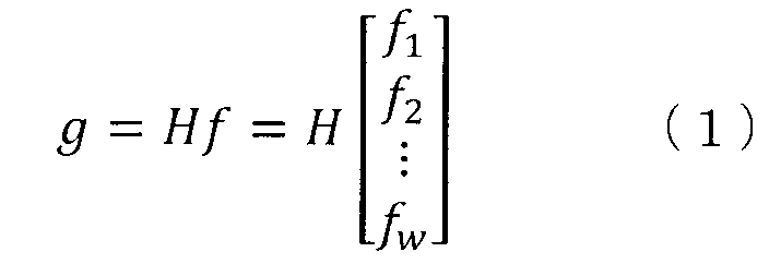
ここで、f1、f2、・・・、fwは、n×m個の要素を有するデータである。したがって、右辺のベクトルは、厳密にはn×m×w行1列の1次元ベクトルである。ベクトルgは、n×m行1列の1次元ベクトルに変換して表され、計算される。行列Hは、ベクトルfの各成分f1、f2、・・・、fwを波長バンドごとに異なる符号化情報で符号化および強度変調し、それらを加算する変換を表す。したがって、Hは、n×m行n×m×w列の行列である。
ベクトルgと行列Hが与えられれば、式(1)の逆問題を解くことにより、fを算出することができそうである。しかし、求めるデータfの要素数n×m×wが取得データgの要素数n×mよりも多いため、この問題は不良設定問題であり、このままでは解くことができない。そこで、処理回路200は、データfに含まれる画像の冗長性を利用し、圧縮センシングの手法を用いて解を求める。具体的には、以下の式(2)を解くことにより、求めるデータfが推定される。

ここで、f’は、推定されたfのデータを表す。上式の括弧内の第1項は、推定結果Hfと取得データgとのずれ量、いわゆる残差項を表す。ここでは2乗和を残差項としているが、絶対値あるいは二乗和平方根等を残差項としてもよい。括弧内の第2項は、後述する正則化項または安定化項である。式(2)は、第1項と第2項との和を最小化するfを求めることを意味する。処理回路200は、再帰的な反復演算によって解を収束させ、最終的な解f’を算出することができる。
式(2)の括弧内の第1項は、取得データgと、推定過程のfを行列Hによってシステム変換したHfとの差分の二乗和を求める演算を意味する。第2項のΦ(f)は、fの正則化における制約条件であり、推定データのスパース情報を反映した関数である。働きとしては、推定データを滑らかまたは安定にする効果がある。正則化項は、例えば、fの離散的コサイン変換(DCT)、ウェーブレット変換、フーリエ変換、またはトータルバリエーション(TV)などによって表され得る。例えば、トータルバリエーションを使用した場合、観測データgのノイズの影響を抑えた安定した推測データを取得できる。それぞれの正則化項の空間における対象物70のスパース性は、対象物70のテキスチャによって異なる。対象物70のテキスチャが正則化項の空間においてよりスパースになる正則化項を選んでもよい。あるいは、複数の正則化項を演算に含んでもよい。τは、重み係数である。重み係数τが大きいほど冗長的なデータの削減量が多くなり、圧縮する割合が高まる。重み係数τが小さいほど解への収束性が弱くなる。重み係数τは、fがある程度収束し、かつ、過圧縮にならない適度な値に設定される。
なお、図1Bから図1Dの構成においては、フィルタアレイ10によって符号化された像は、イメージセンサ60の撮像面上でボケた状態で取得される。したがって、予めこのボケ情報を保有しておき、そのボケ情報を前述のシステム行列Hに反映させることにより、分離画像220を再構成することができる。ここで、ボケ情報は、点拡がり関数(Point Spread Function:PSF)によって表される。PSFは、点像の周辺画素への拡がりの程度を規定する関数である。例えば、画像上で1画素に相当する点像が、ボケによってその画素の周囲のk×k画素の領域に広がる場合、PSFは、その領域内の各画素の画素値への影響を示す係数群、すなわち行列として規定され得る。PSFによる符号化パターンのボケの影響を、システム行列Hに反映させることにより、分離画像220を再構成することができる。フィルタアレイ10が配置される位置は任意であるが、フィルタアレイ10の符号化パターンが拡散しすぎて消失しない位置が選択され得る。
なお、ここでは式(2)に示す圧縮センシングを用いた演算例を示したが、その他の方法を用いて解いてもよい。例えば、最尤推定法またはベイズ推定法などの他の統計的方法を用いることができる。また、分離画像220の数は任意であり、各波長バンドも任意に設定してよい。再構成の方法の詳細は、特許文献1に開示されている。特許文献1の開示内容の全体を本明細書に援用する。
<フィルタアレイ10が有する特徴量>
実際にフィルタアレイ10を用いて撮像された画像は、光ショットノイズと呼ばれるランダムノイズを含み得る。ランダムノイズは、検出光量の平方根に比例して増加する。ここでは、図5Aおよび図5Bを参照して、後述のランダムノイズの議論に用いられる、本実施形態によるフィルタアレイ10が有する特徴量を説明する。図5Aは、フィルタアレイ10における複数の波長バンドの各々についての光透過率の空間パターンを模式的に示す図である。当該空間パターンは、モザイクパターンとして表現されている。波長バンドの数をN(Nは4以上の整数)とする。図5Aに示すように、波長バンドごとに、フィルタアレイ10の光透過率の分布が異なる。図5Bは、第i(iは1以上N以下の整数)の波長バンドについて、フィルタアレイ10が有する透過率のヒストグラムの例を模式的に示す図である。図5Bに示す例において、横軸は透過率を表し、縦軸はその透過率を有するフィルタの数を表す。図5Bに示すヒストグラムから、フィルタアレイ10の特徴量として、第iの波長バンドの光についての透過率の平均値μiおよび有限の標準偏差σiが得られる。図5Bに示すヒストグラムがガウス分布を有する場合、透過率がμi-σi以上μi+σi以下の範囲内に含まれるフィルタの数は、全体の約68%を占める。透過率がμi-2σi以上μi+2σi以下の範囲内に含まれるフィルタの数は、全体の約95%を占める。図5Bに示すように、μi-2σiの値が大きければ、高い透過率を有するフィルタの数が増加する。σiが大きければ、フィルタ100同士の分別が容易である。
実際にフィルタアレイ10を用いて撮像された画像は、光ショットノイズと呼ばれるランダムノイズを含み得る。ランダムノイズは、検出光量の平方根に比例して増加する。ここでは、図5Aおよび図5Bを参照して、後述のランダムノイズの議論に用いられる、本実施形態によるフィルタアレイ10が有する特徴量を説明する。図5Aは、フィルタアレイ10における複数の波長バンドの各々についての光透過率の空間パターンを模式的に示す図である。当該空間パターンは、モザイクパターンとして表現されている。波長バンドの数をN(Nは4以上の整数)とする。図5Aに示すように、波長バンドごとに、フィルタアレイ10の光透過率の分布が異なる。図5Bは、第i(iは1以上N以下の整数)の波長バンドについて、フィルタアレイ10が有する透過率のヒストグラムの例を模式的に示す図である。図5Bに示す例において、横軸は透過率を表し、縦軸はその透過率を有するフィルタの数を表す。図5Bに示すヒストグラムから、フィルタアレイ10の特徴量として、第iの波長バンドの光についての透過率の平均値μiおよび有限の標準偏差σiが得られる。図5Bに示すヒストグラムがガウス分布を有する場合、透過率がμi-σi以上μi+σi以下の範囲内に含まれるフィルタの数は、全体の約68%を占める。透過率がμi-2σi以上μi+2σi以下の範囲内に含まれるフィルタの数は、全体の約95%を占める。図5Bに示すように、μi-2σiの値が大きければ、高い透過率を有するフィルタの数が増加する。σiが大きければ、フィルタ100同士の分別が容易である。
ヒストグラムは、フィルタアレイ10における各光学フィルタの透過率を、所定の階調数で光強度を検出する光検出器を用いて計測することによって得ることができる。例えば、8ビットまたは16ビットなどの所定の階調数で光強度の2次元分布を検出できるイメージセンサなどの光検出器を用いてヒストグラムを得ることができる。具体的には、フィルタアレイ10が配置された状態で検出された第iの波長バンドの光の強度と、フィルタアレイ10が配置されていない状態で検出された第iの波長バンドの光の強度との比から、フィルタアレイ10における各フィルタ100の第iの波長バンドの光の透過率を求めることができる。上記の方法によって取得された各フィルタ100の透過率のデータから、図5Bに示されるようなヒストグラムを得ることができる。なお、実際のフィルタアレイ10では、図5Bとは異なる形状のヒストグラムが取得され得る。透過率の波長依存性がフィルタによって異なることから、ヒストグラムの形状は波長バンドごとに異なる。したがって、複数のフィルタ100の透過率の平均値および標準偏差も、波長バンドごとに異なる。
以下の説明において、透過率のヒストグラムの階調数は8ビットであるものとする。光強度が8ビット以外の階調数で検出されたとしても、当該強度を8ビットの階調数に変換して透過率のヒストグラムを求めることができる。
<ランダムノイズが分離画像に及ぼす影響>
次に、図6Aから図7Bを参照して、ランダムノイズが分離画像に及ぼす影響を説明する。
次に、図6Aから図7Bを参照して、ランダムノイズが分離画像に及ぼす影響を説明する。
図6Aは、元画像にランダムノイズが重畳された撮像画像の例を模式的に示す図である。図6Aに示すように、ランダムノイズを含む撮像画像は、元画像と比較して不鮮明になり得る。図6Bは、ランダムノイズを含む撮像画像データgが行列Hおよび分離画像データfの積によって表される式(1)の関係を模式的に示す図である。図6Bに示す行列Hは、図5Aに示す波長バンドごとの透過率の空間分布の成分を含む。
図7Aは、本実施形態とは異なるフィルタアレイに含まれるあるフィルタの透過スペクトルの例を示す図である。図7Aに示す例において、対象波長域Wは、450nm以上850nm以下の範囲である。対象波長域Wは、各バンド幅が80nmである5個の波長バンドを含む。図7Aに示す例において、透過スペクトルは、8本の鋭いピークを有する。透過率の最大値は約1であり、最小値は約0.02である。互いに隣接する2つのピークの間での透過率は十分に低い。このような透過スペクトルを有するフィルタ100は、対象波長域W内の反射率が高い2つの反射層、およびそれらの間の干渉層を含む共振構造によって実現される。干渉層の屈折率および/または厚さを変化させることにより、透過スペクトルは長波長側または短波長側にシフトする。当該フィルタアレイは、そのようにして透過スペクトルがシフトした複数種類のフィルタを含む。当該フィルタアレイは、2次元的に配列された100万個のフィルタを備える。当該100万個のフィルタは、ランダム分布または準ランダム分布で配列された16種類のフィルタを含む。
図7Bは、上記のフィルタアレイを用いて撮像された画像がランダムノイズを含む場合における、5つの波長バンドでの正解画像と分離画像との間の平均2乗誤差(Mean Squared Error:MSE)を示す図である。ランダムノイズは、中心がμnoise=0であり、標準偏差がσnoiseであるガウス分布に従い発生されている。各画素に加算されるランダムノイズの分散Nnoiseは、以下の式(3)を用いて計算される。

ここで、gnoiseは各画素に重畳されるノイズの値であり、正の値も負の値も取り得る。図7Bに示す例では、σnoise=0、5、および10である。σnoise=0は、ランダムノイズが存在しないことを意味する。σnoiseが増加すると、ランダムノイズは増加する。平均2乗誤差は、以下の式(4)を用いて計算される。

ここで、NおよびMは、それぞれ横方向および縦方向の画素数である。Ii、jは、位置(i、j)の画素における正解画像の画素値である。I’i、jは、位置(i、j)の画素における分離画像の画素値である。
図7Bに示すように、σnoiseが増加するにつれて、5個すべての波長バンドでのMSEが増加することがわかる。ランダムノイズが存在しない場合、図7Aに示すような、透過率の最大値および最小値のコントラスト比が大きい透過スペクトルを有するフィルタは、波長バンド間のSN比を向上させることができる。すなわち、図5Aに示す、波長バンド間での透過率の空間分布の差異が明確になる。しかし、当該フィルタを含むフィルタアレイは、ランダムノイズの影響を受けやすい。その結果、ハイパースペクトルカメラの波長分解能が低下し得る。
<ノイズ耐性を有するフィルタアレイ10>
以下に、上記の課題を解決することが可能な本実施形態によるフィルタアレイ10を説明する。図5Bに示すμi-2σiの値が大きいフィルタアレイ10は、ノイズ耐性を有する。そのようなフィルタアレイ10では、透過率が高いからである。一方、図5Bに示すσiが大きいフィルタアレイ10もまた、ノイズ耐性を有する。そのようなフィルタアレイ10では、フィルタ間の透過率の分散が大きくフィルタ100同士の分別が容易であるため、分離画像の復元精度が向上するからである。以上のことから、μi-2σiおよびσiの和であるMi=μi-σiをノイズ耐性の指標として、本実施形態によるフィルタアレイ10の光学特性を説明する。なお、本実施形態によるフィルタアレイ10は、前述した例と同様に、ランダム分布または準ランダム分布で配列された複数種類のフィルタを含む。
以下に、上記の課題を解決することが可能な本実施形態によるフィルタアレイ10を説明する。図5Bに示すμi-2σiの値が大きいフィルタアレイ10は、ノイズ耐性を有する。そのようなフィルタアレイ10では、透過率が高いからである。一方、図5Bに示すσiが大きいフィルタアレイ10もまた、ノイズ耐性を有する。そのようなフィルタアレイ10では、フィルタ間の透過率の分散が大きくフィルタ100同士の分別が容易であるため、分離画像の復元精度が向上するからである。以上のことから、μi-2σiおよびσiの和であるMi=μi-σiをノイズ耐性の指標として、本実施形態によるフィルタアレイ10の光学特性を説明する。なお、本実施形態によるフィルタアレイ10は、前述した例と同様に、ランダム分布または準ランダム分布で配列された複数種類のフィルタを含む。
図8は、複数の波長バンドの各々についてσi=0.08である場合における、複数の波長バンドでの正解画像と分離画像との間の平均MSEと、Mi=μi-σiとの関係を示す図である。図8に示す例において、ランダムノイズの標準偏差はσnoise=0、2、3、4、および5である。フィルタアレイ10の透過光量はMiに依存する。Miの値が小さいほど、フィルタアレイ10の透過光量は減少し、Miの値が大きいほど、フィルタアレイ10の透過光量は増加する。フィルタアレイ10に含まれる複数のフィルタ100のうち、大部分の透過率が低く、一部の透過率が高い場合、フィルタアレイ10の透過率のヒストグラムは非対称になり得る。そのようなフィルタアレイ10では、Miは負の値にもなり得る。
σnoise=0の場合、撮像画像はランダムノイズを含まない。この場合、Mi≦0.45では、平均MSEが低く抑えられる。図7Aに示すように、フィルタ100における透過率のコントラスト比が高い場合、フィルタアレイ10の平均的な透過光量は少なく、Miの値は小さい。そのようなフィルタアレイ10は、波長バンド間のSN比を向上させる。その結果、分離画像の復元誤差の発生を抑制することができる。これに対して、Mi>0.45では、平均MSEがMiの増加に伴って増加する。フィルタ100における透過率のコントラスト比が低い場合、フィルタアレイ10の平均的な透過光量は多く、Miの値は大きい。そのようなフィルタアレイ10は、波長バンド間のSN比を低下させる。その結果、分離画像の復元誤差は増加する。
σnoise>0の場合、Mi<0.2では、実線の楕円によって囲まれた領域に示すように、平均MSEが、σnoiseの増加に伴って大きく増加する。これに対して、Mi=0.42付近では、破線の楕円によって囲まれた領域に示すように、平均MSEがσnoiseの増加に伴って増加するものの、その増加幅は抑制される。Mi>0.45では、σnoiseが小さくても、平均MSEは、Miの増加に伴って増加する。図8に示すように、σnoise=5の場合、平均MSEが不連続的に急増することがある。上記の特性をまとめると、以下の通りである。
・(Miが小さい場合)波長バンド間のSN比は高い。したがって、σnoiseが小さいとき、分離画像の復元精度は高い。σnoiseが増加すると、フィルタアレイ10の少ない透過光量と比較して、ランダムノイズの量が無視できなくなる。その結果、分離画像の復元精度が大きく低下する。
・(Miが大きすぎる場合)波長バンド間のSN比は低い。したがって、σnoiseが小さくても、分離画像の復元精度は低い。
・(Miが適度に大きい場合)σnoiseが小さいとき、分離画像の復元精度は高い。σnoiseが増加しても、フィルタアレイ10の透過光量と比較して、ランダムノイズの量はそれほど大きくはならない。その結果、分離画像の復元精度の低下が抑制される。
・(Miが小さい場合)波長バンド間のSN比は高い。したがって、σnoiseが小さいとき、分離画像の復元精度は高い。σnoiseが増加すると、フィルタアレイ10の少ない透過光量と比較して、ランダムノイズの量が無視できなくなる。その結果、分離画像の復元精度が大きく低下する。
・(Miが大きすぎる場合)波長バンド間のSN比は低い。したがって、σnoiseが小さくても、分離画像の復元精度は低い。
・(Miが適度に大きい場合)σnoiseが小さいとき、分離画像の復元精度は高い。σnoiseが増加しても、フィルタアレイ10の透過光量と比較して、ランダムノイズの量はそれほど大きくはならない。その結果、分離画像の復元精度の低下が抑制される。
図9Aから図9Cは、それぞれ、複数の波長バンドの各々についてσi=0.05、0.07、および0.1である場合における、複数の波長バンドでの正解画像と分離画像との間の平均MSEと、Mi=μi-σiとの関係を示す図である。図9Aから図9Cに示すように、Miが適度に大きい場合、σnoiseが増加しても、分離画像の復元精度の低下が抑制される。そのようなMiは約0.3以上約0.5以下の範囲にある。実際には、ランダムノイズによる復元誤差に加えて、読み出しノイズのような他のノイズによる復元誤差が数%程度存在する。これらの合算された復元誤差が5%を超えると、分離画像の復元精度の低さが視認され得る。したがって、許容されるランダムノイズによる復元誤差は、例えば3%以下であり得る。8ビット階調において、3%の復元誤差は平均MSE=56である。図9Aから図9Cに示す例において、実際のランダムノイズに近いσnoise=5の場合、平均MSEが56を下回るときのMiの下限は、Mi=0.1である。以上から、Mi≧0.1を有するフィルタアレイ10は、ランダムノイズに対してロバストであると言うことができる。
本実施形態によるフィルタアレイ10は、Mi≧0.1以外にも以下の特性を有する。
・複数の波長バンドの各々についてσi≧0.05である。この場合、フィルタ100同士の分別が容易であることから、分離画像の復元精度を向上させることができる。
・複数の波長バンドの各々についてμi≧0.2である。この場合、図8から図9Cに示す0.05≦σi≦0.1についてMi≧0.1が満たされる。
・複数の波長バンドについて最大のMiおよび最小のMiをそれぞれMmaxおよびMminとすると、Mmax/Mmin≦3である。この場合、複数の波長バンド間での分離画像の復元精度がばらつくことを抑制することができる。
・複数の波長バンドの各々についてσi≧0.05である。この場合、フィルタ100同士の分別が容易であることから、分離画像の復元精度を向上させることができる。
・複数の波長バンドの各々についてμi≧0.2である。この場合、図8から図9Cに示す0.05≦σi≦0.1についてMi≧0.1が満たされる。
・複数の波長バンドについて最大のMiおよび最小のMiをそれぞれMmaxおよびMminとすると、Mmax/Mmin≦3である。この場合、複数の波長バンド間での分離画像の復元精度がばらつくことを抑制することができる。
<フィルタアレイの具体的な構造>
次に、図10Aおよび図10Bを参照して、複数の波長バンドの各々についてMi≧0.1を満たす本実施形態によるフィルタアレイ10の具体的な構造の例を説明する。図10Aおよび図10Bは、それぞれ、光検出装置300の第1の例および第2の例を模式的に示す断面図である。当該断面図は、図2Aに示すフィルタアレイ10の1つの行およびイメージセンサ60の断面構造の例を示す。図10Aおよび図10Bに示す例では、フィルタアレイ10がイメージセンサ60上に配置されている。イメージセンサ60に含まれる複数の光検出素子60aは、それぞれ、フィルタアレイ10に含まれる複数のフィルタ100の直下に位置する。フィルタアレイ10とイメージセンサ60とが分離していてもよい。その場合であっても、複数の光検出素子60aの各々は、複数のフィルタの1つを透過した光を受ける位置に配置され得る。複数のフィルタを透過した光が、ミラーを介して複数の光検出素子60aにそれぞれ入射するように、各構成要素が配置されていてもよい。その場合、複数の光検出素子60aの各々は、複数のフィルタの1つの直下には配置されない。
次に、図10Aおよび図10Bを参照して、複数の波長バンドの各々についてMi≧0.1を満たす本実施形態によるフィルタアレイ10の具体的な構造の例を説明する。図10Aおよび図10Bは、それぞれ、光検出装置300の第1の例および第2の例を模式的に示す断面図である。当該断面図は、図2Aに示すフィルタアレイ10の1つの行およびイメージセンサ60の断面構造の例を示す。図10Aおよび図10Bに示す例では、フィルタアレイ10がイメージセンサ60上に配置されている。イメージセンサ60に含まれる複数の光検出素子60aは、それぞれ、フィルタアレイ10に含まれる複数のフィルタ100の直下に位置する。フィルタアレイ10とイメージセンサ60とが分離していてもよい。その場合であっても、複数の光検出素子60aの各々は、複数のフィルタの1つを透過した光を受ける位置に配置され得る。複数のフィルタを透過した光が、ミラーを介して複数の光検出素子60aにそれぞれ入射するように、各構成要素が配置されていてもよい。その場合、複数の光検出素子60aの各々は、複数のフィルタの1つの直下には配置されない。
本実施形態によるフィルタアレイ10に含まれるすべてのフィルタ100は共振構造を備える。共振構造とは、ある波長の光が、内部で定在波を形成して安定に存在する構造を意味する。図10Aに示す共振構造は、積層された基板22、反射層24、および干渉層26をこの順に含む。図10Bに示す共振構造は、積層された基板22、干渉層26、および反射層24をこの順に含む。図10Aおよび図10Bに示す基板22は、すべてのフィルタ100に亘り段差なく一様に設けられている。図10Aに示す反射層24は、図10Bに示す反射層24とは異なり、すべてのフィルタ100に亘り段差なく一様に設けられている。図10Aおよび図10Bに示すように、干渉層26および反射層24の積層の順番は任意である。基板22は必ずしも必要ではない。反射層24は、例えば、分布ブラッグ反射器(Distributed Bragg Reflector:DBR)を含み得る。反射層24の構成の詳細については後述する。干渉層26の屈折率および/または厚さは、フィルタ100によって異なり得る。複数のフィルタ100の透過スペクトルは、干渉層26の屈折率および/または厚さに応じて異なる。各フィルタ100の透過スペクトルは、対象波長域Wにおいて複数の波長で透過率の極大値を有する。
なお、本実施形態によるフィルタアレイ10では、複数のフィルタ100のうち、少なくとも1つのフィルタが上記の共振構造を有する一方、他のフィルタは上記の共振構造を有していなくてもよい。例えば、フィルタアレイ10は、透明フィルタまたはNDフィルタ(Neutral Density Filter)などの、光透過率の波長依存性を有しないフィルタを含んでいてもよい。
第1の例において、干渉層26は大気に露出していてもよい。干渉層26の表面上に空間を空けてレンズおよび保護カバーなどの部材が配置されていてもよい。このとき、当該空間は大気で満たされていてもよいし、窒素ガスなどのガスによって封止されていてもよい。第2の例における反射層24の表面についても同様である。
次に、図11Aを参照して、フィルタ100の構成の例を説明する。図11Aは、図10Aに示すフィルタ100の例を模式的に示す図である。図11Aに示すように、反射層24は、複数の第1屈折率層24aおよび複数の第2屈折率層24bが交互に積層されたDBRを含む。DBRは、屈折率が異なる第1屈折率層24aおよび第2屈折率層24bのペア層を1組以上含む。第1屈折率層24aの屈折率は、第2屈折率層24bの屈折率よりも高い。分布ブラッグ反射器は、周期構造に起因するブラッグ反射により、反射率が高い波長域を有する。当該波長域はストップバンドと呼ばれる。上記のペア層の数を増加させると、ストップバンドの反射率は100%に近づく。
対象波長域W内の波長をλ、第1屈折率層24aの屈折率をnH、第2屈折率層24bの屈折率をnLとする。厚さがλ/(4nH)である第1屈折率層24a、および厚さがλ/(4nL)である第2屈折率層24bのペア層を1組以上含むDBRは、波長λの光を効率的に反射させる。対象波長域Wが波長λi以上波長λf以下の範囲である場合、複数の第1屈折率層24aおよび複数の第2屈折率層24bの厚さを段階的に変化させることにより、DBRは、波長λiに対応するペア層から波長λfに対応するペア層を含むことができる。その結果、当該DBRは、対象波長域W内のすべての光を効率的に反射させることができる。
DBRは、例えば、対象波長域W内の光について吸収率の低い材料から形成され得る。対象波長域Wが可視光領域内にある場合、当該材料は、例えば、SiO2、Al2O3、SiOxNy、Si3N4、Ta2O5、およびTiO2からなる群から選択される少なくとも1つであり得る。対象波長域Wが赤外領域内にある場合、当該材料は、例えば、上記のSiO2、Al2O3、SiOxNy、Si3N4、Ta2O5、およびTiO2に加えて、単結晶Si、多結晶Si、およびアモルファスSiからなる群から選択される少なくとも1つであり得る。
干渉層26は、反射層24に接する下面26s1およびその反対側の上面26s2を有する。図11Aに示すフィルタ100において、下面26s1が第1表面に相当し、上面26s2が第2表面に相当する。図11Aに示す例では、上面26s2は、外部に露出し、空気に接している。干渉層26上に、透明層をさらに積層してもよい。この場合、上面26s2は、当該透明層に接する。下面26s1における対象波長域Wの光についての反射率(以下、「第1反射率」と称する。)は、例えば80%以上であり得る。第1反射率は、80%よりも低くてもよいが、反射を抑制する観点から、40%以上に設計され得る。上面26s2における対象波長域Wの光についての反射率(「第2反射率」と称する。)は、第1反射率よりも低く、例えば1%以上30%未満であり得る。第1反射率と第2反射率との間には10%以上の一定の差異がある。
一方、図10Bに示す光検出装置300のフィルタ100においては、干渉層26の上面上に反射層24が配置されている。図10Bに示す光検出装置300のフィルタ100において、干渉層26の上面が第1表面に相当し、下面が第2表面に相当する。
本明細書では、光を反射する面の正確な位置が問題にならない限り、干渉層26内の光は、下面26s1および上面26s2で反射されるものとする。本実施形態において、干渉層26から反射層24に入射する光の一部は、実際には、反射層24内に浸入し、複数の第1屈折率層24aおよび複数の第2屈折率層24bの界面で反射される。光が反射される界面は、波長によって異なる。しかし、説明の便宜上、これらの光は、下面26s1で反射されるものとして取り扱う。
下面26s1および上面26s2での光の反射により、干渉層26内には複数の定在波が形成される。その結果、干渉層26の厚さが所定値以上である場合、フィルタ100の透過スペクトルは、対象波長域Wにおいて複数の波長で透過率の極大値を有する。言い換えれば、フィルタ100の透過スペクトルは、対象波長域W内に複数のピークを有する。本明細書では、このようなフィルタを、「多モードフィルタ」と称する。DBRが波長λに対応するペア層を含む場合、多モードフィルタを実現できる干渉層26の厚さは、例えば、第1屈折率層24aの厚さの2倍以上、すなわちλ/(2nH)以上であり得る。干渉層26の厚さではなく、干渉層26の屈折率を適切に設計して多モードフィルタを実現してもよい。あるいは、干渉層26の厚さおよび屈折率の両方を適切に設計して多モードフィルタを実現してもよい。
干渉層26は、DBRと同様の材料から形成され得る。干渉層26は、単一の層に限らず、積層された複数の層を含んでいてもよい。当該複数の層は、異なる材料から形成されていてもよい。当該複数の層の屈折率は、フィルタ100の透過スペクトルに実質的な影響を与えない程度に異なっていてもよい。屈折率が異なる層の界面では反射が生じ得る。しかし、透過スペクトルに実質的な影響を与えない程度であれば、当該複数の層の各々は、実質的に一様な干渉層26の一部として考えることができる。許容される屈折率の相対誤差は0%以上9%以下である。当該相対誤差は、最大屈折率と最小屈折率との差の絶対値を最大の屈折率によって割った値である。例えば、Ta2O5およびSi3N4の可視光領域における屈折率は、それぞれ2.2および2.05である。これらの屈折率の相対誤差はおよそ7%である。したがって、積層されたTa2O5層およびSi3N4層の各々は、実質的に一様な干渉層26の一部であると考えることができる。
以下の説明において、図11Aに示す構造を、「片側DBR構造」と称する。図11Aに示す構造に加えて、干渉層26上に反射層24がさらに積層された構造を、「両側DBR構造」と称する。片側DBR構造において、干渉層26の下面26s1および上面26s2のうち、一方には反射層24が設けられ、他方には設けられない、両側DBR構造において、干渉層26の下面26s1および上面26s2の両方に反射層が設けられている。
次に、図11Bを参照して、フィルタ100の透過スペクトルの例を説明する。図11Bは、光が垂直に入射する場合における片側DBR構造および両側DBR構造の光の透過スペクトルの例を示す図である。図11Bに示す例において、対象波長域Wは450nm以上850nm以下である。図11Bに示す実線は、片側DBR構造の透過スペクトルを表す。図11Bに示す破線は、両側DBR構造の透過スペクトルを表す。図11Bに示すように、片側DBR構造および両側DBR構造の両方から多モードフィルタを得ることができる。ただし、両者の多モードフィルタの特性は以下の点において異なる。片側DBR構造の透過スペクトルにおいて、複数のピークの各々は幅広く、かつ、最大の透過率が0.5程度であり、最小の透過率が0.1程度である。すなわち、透過率のコントラスト比は低い。これに対して、両側DBR構造の透過スペクトルにおいて、複数のピークの各々は鋭く、かつ、最大の透過率が1.0程度であり、最小の透過率が0.02程度である。すなわち、透過率のコントラスト比は高い。
片側DBR構造では、両側DBR構造と比較して、透過率のベースラインが上昇する。この例において、片側DBR構造での対象波長域W内の平均透過率は約0.26であり、両側DBR構造での対象波長域W内の平均透過率は約0.1である。片側DBR構造では、両側DBR構造と比較して、平均透過率が約2倍である。このように、片側DBR構造は、撮像時の光量損失を抑制することができる。
図11Bに示す例において、片側DBR構造および両側DBR構造では、それぞれ、複数の波長バンドの各々についてMi=0.1およびMi=-0.14である。フィルタアレイ10に含まれる複数のフィルタ100がそれぞれ複数の片側DBR構造を含む場合、複数の波長バンドの各々についてMi≧0.1を満たすことができる。
次に、図12Aおよび図12Bを参照して、複数の波長バンドの各々についてMi≧0.1を満たす本実施形態によるフィルタアレイ10の具体的な構造の他の例を説明する。図12Aおよび図12Bは、それぞれ、光検出装置300の第3の例および第4の例を模式的に示す断面図である。第3の例および第4の例では、それぞれ、第1の例および第2の例とは異なり、反射層25がDBRではなく金属膜を含む。金属膜の対象波長域Wにおける反射率は、金属膜の材料に依存する。金属膜の対象波長域Wにおける吸収係数は、金属膜の厚さに依存する。
金属膜は、対象波長域Wにおける反射率が例えば90%以上である材料から形成され得る。対象波長域Wが可視光領域内にある場合、反射率が90%以上である金属膜の材料は、例えば、AgおよびAlからなる群から選択される少なくとも1つであり得る。対象波長域Wが赤外領域内にある場合、反射率が90%以上である金属膜の材料は、Ag、Al、Au,およびCuからなる群から選択される少なくとも1つであり得る。反射率が相対的に低い金属膜であっても、反射率を抑制する点では有用である。例えば、対象波長域Wにおける反射率が40%以上70%以下の材料から金属膜が形成されていてもよい。対象波長域Wが可視光領域または赤外領域内にある場合、反射率が40%以上70%以下である金属膜の材料は、例えば、NiおよびPtからなる群から選択される少なくとも1つであり得る。金属膜は合金であってもよい。金属膜はメッキ加工によって設けられてもよい。
金属膜の厚さは、例えば1nm以上100nm以下であり得る。この場合、金属膜の可視光領域から近赤外領域における透過率は相対的に大きくなり得る。その結果、可視光領域から近赤外領域における光は、金属膜を効果的に透過することができる。金属膜の厚さは数十nm以下であってもよい。
図10Aおよび図10Bならびに図12Aおよび図12Bに示す例では、干渉層26の片側にのみ反射層が存在した。干渉層26における第1反射率および第2反射率が上記のように一定の差異を有していれば、干渉層26の両側に反射層が存在してもよい。
次に、図13Aおよび図13Bを参照して、複数の波長バンドの各々についてMi≧0.1を満たす本実施形態によるフィルタアレイ10の具体的な構造のさらに他の例を説明する。
図13Aは、光検出装置300の第5の例を模式的に示す斜視図である。図13Aに示す例において、フィルタアレイ10は、複数のフィルタ110を含む。複数のフィルタ110の各々は、複数のサブフィルタ30が配列されたサブフィルタアレイである。フィルタアレイ10は、複数のフィルタ110を通過した光が、イメージセンサ60における複数の光検出素子60aにそれぞれ入射するように配置されている。図13Aに示す例では、1つの光検出素子60aが、4×4個のサブフィルタ30を透過する光を検出する。なお、すべてのフィルタがサブフィルタアレイである必要はない。本実施形態によるフィルタアレイは、少なくとも1つのサブフィルタアレイを含み得る。
図13Bは、サブフィルタアレイであるフィルタ110および光検出素子60aの例を模式的に示す斜視図である。複数のサブフィルタ30は、透過波長域が互いに異なる複数種類の第1サブフィルタ30aと、複数の波長バンドのそれぞれの光を透過させる1つ以上の第2サブフィルタ30bとを含む。図13Bに示す例では、ハッチングが付されたサブフィルタが第1サブフィルタ30aを表し、白色のサブフィルタが第2サブフィルタ30bを表す。第1サブフィルタ30aの個数および第2サブフィルタ30bの個数は、サブフィルタアレイであるフィルタ110ごとに異なる。複数のサブフィルタアレイであるフィルタ110は、互いに異なる透過スペクトルを有する。
複数種類の第1サブフィルタ30aは、例えば、赤フィルタ、緑フィルタ、および青フィルタのRGBカラーフィルタを含み得る。複数種類の第1サブフィルタ30aは、RGBカラーフィルタの代わりに、またはRBGフィルタに加えて、シアンフィルタ、マゼンタフィルタ、および黄フィルタのCMYフィルタの少なくとも1つを含んでいてもよい。第2サブフィルタ30bは、例えば可視光領域において高い透過率を有する透明フィルタであり得る。第2サブフィルタ30bではなく、開口部であってもよい。第2サブフィルタ30bまたは開口部により、図13Bに示すフィルタ110の透過率のベースラインを上昇させることができる。その結果、図13Aに示すフィルタアレイ10は、複数の波長バンドの各々についてMi>0.1を満たすことができる。そのようなフィルタアレイ10はノイズ耐性を有する。サブフィルタアレイであるフィルタ110の全体の面積に占める第2サブフィルタ30bまたは開口部の面積の割合は4%以上である。4%の割合は、例えば、5×5のサブフィルタ30が1個の第2サブフィルタ30bを含む場合に相当する。
次に、図14を参照して、サブフィルタアレイであるフィルタ110の透過スペクトルの例を説明する。図14は、8種類のサブフィルタアレイの透過スペクトルの例を示す図である。各サブフィルタアレイであるフィルタ110における4×4個のサブフィルタ30は、3種類のRBGカラーフィルタが配列された14個の第1サブフィルタ30aと、白色光を透過させる2個の第2サブフィルタ30bとを含む。サブフィルタアレイであるフィルタ110の全体の面積に占める第2サブフィルタ30bの面積の割合は、12.5%である。第2サブフィルタ30bにより、すべてのサブフィルタアレイの透過スペクトルにおける最小の透過率は0.15以上である。その結果、複数の波長バンドの各々についてMi=0.18程度であり、Mi>0.1が満たされる。これに対して、各サブフィルタアレイにおける4×4個のサブフィルタ30がすべて第1サブフィルタ30aである場合、複数の波長バンドの各々についてMi=0.05程度であり、Mi>0.1が満たされない。
なお、Miが大きすぎる場合、複数のサブフィルタ30の一部にNDフィルタを含めることにより、サブフィルタアレイであるフィルタ110の透過率の最小値を減少させることができる。その結果、Miの値が減少する。
本開示における光検出システム、およびフィルタアレイは、例えば、多波長の2次元画像を取得するカメラおよび測定機器に有用である。本開示における光検出システム、およびフィルタアレイは、生体・医療・美容向けセンシング、食品の異物・残留農薬検査システム、リモートセンシングシステムおよび車載センシングシステム等にも応用できる。
10 フィルタアレイ
24、25 反射層
26 干渉層
26s1 下面
26s2 上面
30 サブフィルタ
30a 第1サブフィルタ
30b 第2サブフィルタ
40 光学系
60 イメージセンサ
60a 光検出素子
70 対象物
100 フィルタ
110 フィルタ、サブフィルタアレイ
120 画像
200 処理回路
220 分離画像
300 光検出装置
400 光検出システム
24、25 反射層
26 干渉層
26s1 下面
26s2 上面
30 サブフィルタ
30a 第1サブフィルタ
30b 第2サブフィルタ
40 光学系
60 イメージセンサ
60a 光検出素子
70 対象物
100 フィルタ
110 フィルタ、サブフィルタアレイ
120 画像
200 処理回路
220 分離画像
300 光検出装置
400 光検出システム
Claims (13)
- 特定の波長域に含まれるN個(Nは2以上の整数)の波長バンドのそれぞれに対応する画像データを生成する光検出装置において用いられるフィルタアレイであって、
複数の光学フィルタを備え、
前記複数の光学フィルタは、前記N個の波長バンドの各々についての光透過率が互いに異なる複数種類の光学フィルタを含み、
前記N個の波長バンドのうちの第iの波長バンド(iは1以上N以下の整数)に含まれる波長を有する光についての前記複数の光学フィルタの光透過率の平均値をμiとし、前記第iの波長バンドに含まれる波長を有する前記光についての前記複数の光学フィルタの前記光透過率の標準偏差をσiとし、Mi=μi-σiとすると、
前記N個の波長バンドの各々について、Mi≧0.1である、
フィルタアレイ。 - 前記N個の波長バンドの各々について、σi≧0.05である、
請求項1に記載のフィルタアレイ。 - 前記N個の波長バンドの各々について、μi≧0.2である、
請求項1または2に記載のフィルタアレイ。 - 前記N個の波長バンドについて、最大のMiをMmaxとし、最小のMiをMminとすると、
Mmax/Mmin≦3である、
請求項1から3のいずれかに記載のフィルタアレイ。 - 前記複数の光学フィルタのうちの少なくとも1つの光学フィルタは、
第1表面、および前記第1表面の反対側の第2表面を有する干渉層、及び
前記第1表面上に設けられた反射層を含み、
前記少なくとも1つの光学フィルタの透過スペクトルは、前記特定の波長域に複数の極大値を有し、
前記反射層は、前記第2表面上には設けられていない、
請求項1から4のいずれかに記載のフィルタアレイ。 - 前記反射層は、分布ブラッグ反射器および金属膜からなる群から選択される少なくとも1つを含む、請求項5に記載のフィルタアレイ。
- 前記分布ブラッグ反射器は、第1屈折率層および第2屈折率層の組を1組以上含み、
前記第1屈折率層の屈折率は、前記第2屈折率層の屈折率よりも高い、
請求項6に記載のフィルタアレイ。 - 前記特定の波長域に含まれる波長をλとし、
前記第1屈折率層の前記屈折率をnHとし、前記第2屈折率層の前記屈折率をnLとすると、
前記第1屈折率層の厚さはλ/(4nH)であり、前記第2屈折率層の厚さはλ/(4nL)であり、
前記干渉層の厚さはλ/(2nH)よりも大きい、
請求項7に記載のフィルタアレイ。 - 前記金属膜の厚さは1nm以上100nm以下である、
請求項6に記載のフィルタアレイ。 - 前記光検出装置はイメージセンサを含み、
前記フィルタアレイは、前記複数の光学フィルタを通過した光が前記イメージセンサに入射するように配置され、
前記複数の光学フィルタの少なくとも1つは、2次元的に配列された複数のサブフィルタを含むサブフィルタアレイであり、
前記サブフィルタアレイは、透過波長域が互いに異なる複数種類の第1サブフィルタと、各々が、前記N個の波長バンドのうちの対応する波長バンドに含まれる波長を有するN個の光を透過させる1つ以上の第2サブフィルタまたは開口部と、を含み、
前記サブフィルタアレイの全体の面積に占める、前記1つ以上の第2サブフィルタまたは前記開口部の面積の割合は4%以上である、
請求項1から4のいずれかに記載のフィルタアレイ。 - 前記複数種類の第1サブフィルタは、赤フィルタ、緑フィルタ、および青フィルタを含む、
請求項10に記載のフィルタアレイ。 - 請求項1から11のいずれかに記載のフィルタアレイと、
前記複数の光学フィルタを透過した光を受ける位置に配置され、前記特定の波長域に含まれる波長を有する光に感度を有するイメージセンサと、
を備える、
光検出システム。 - 前記複数の光学フィルタの前記光透過率の空間分布を示すデータと、前記イメージセンサによって取得された圧縮画像データとに基づいて、前記画像データを生成する処理回路、をさらに備える、
請求項12に記載の光検出システム。
Priority Applications (4)
| Application Number | Priority Date | Filing Date | Title |
|---|---|---|---|
| CN202180036101.2A CN115668008B (zh) | 2020-05-29 | 2021-05-10 | 滤波器阵列及光检测系统 |
| JP2022514144A JP7142251B2 (ja) | 2020-05-29 | 2021-05-10 | フィルタアレイおよび光検出システム |
| EP21813748.7A EP4160169A4 (en) | 2020-05-29 | 2021-05-10 | FILTER ARRANGEMENT AND OPTICAL DETECTION SYSTEM |
| US18/054,570 US12529598B2 (en) | 2020-05-29 | 2022-11-11 | Filter array and light detection system |
Applications Claiming Priority (2)
| Application Number | Priority Date | Filing Date | Title |
|---|---|---|---|
| JP2020093886 | 2020-05-29 | ||
| JP2020-093886 | 2020-05-29 |
Related Child Applications (1)
| Application Number | Title | Priority Date | Filing Date |
|---|---|---|---|
| US18/054,570 Continuation US12529598B2 (en) | 2020-05-29 | 2022-11-11 | Filter array and light detection system |
Publications (1)
| Publication Number | Publication Date |
|---|---|
| WO2021241171A1 true WO2021241171A1 (ja) | 2021-12-02 |
Family
ID=78723364
Family Applications (1)
| Application Number | Title | Priority Date | Filing Date |
|---|---|---|---|
| PCT/JP2021/017617 Ceased WO2021241171A1 (ja) | 2020-05-29 | 2021-05-10 | フィルタアレイおよび光検出システム |
Country Status (5)
| Country | Link |
|---|---|
| US (1) | US12529598B2 (ja) |
| EP (1) | EP4160169A4 (ja) |
| JP (1) | JP7142251B2 (ja) |
| CN (1) | CN115668008B (ja) |
| WO (1) | WO2021241171A1 (ja) |
Cited By (2)
| Publication number | Priority date | Publication date | Assignee | Title |
|---|---|---|---|---|
| WO2024142683A1 (ja) | 2022-12-27 | 2024-07-04 | パナソニックIpマネジメント株式会社 | 光検出装置、光検出システム、およびフィルタアレイ |
| EP4492103A4 (en) * | 2022-03-11 | 2025-06-25 | Panasonic Intellectual Property Management Co., Ltd. | Light detection device, light detection system, and filter array |
Families Citing this family (5)
| Publication number | Priority date | Publication date | Assignee | Title |
|---|---|---|---|---|
| WO2021241122A1 (ja) * | 2020-05-29 | 2021-12-02 | パナソニックIpマネジメント株式会社 | フィルタアレイおよび光検出システム |
| US12148775B2 (en) * | 2020-10-13 | 2024-11-19 | Samsung Electronics Co., Ltd. | Hyperspectral element, hyperspectral sensor including the same, and hyperspectral image generating apparatus |
| WO2025047424A1 (ja) * | 2023-08-30 | 2025-03-06 | ソニーセミコンダクタソリューションズ株式会社 | 撮像装置 |
| US20250180928A1 (en) * | 2023-11-30 | 2025-06-05 | Enchroma, Inc. | Filters to enhance color vision |
| CN120213222B (zh) * | 2025-05-26 | 2025-08-15 | 深圳市中达瑞和科技有限公司 | 马赛克滤波片与传感器芯片的耦合方法、系统及存储介质 |
Citations (5)
| Publication number | Priority date | Publication date | Assignee | Title |
|---|---|---|---|---|
| JP2007278950A (ja) * | 2006-04-10 | 2007-10-25 | Canon Inc | マルチバンド撮像装置およびカラーフィルタの特性設定方法 |
| JP2016156801A (ja) * | 2014-11-19 | 2016-09-01 | パナソニックIpマネジメント株式会社 | 撮像装置および分光システム |
| US9466628B2 (en) | 2012-12-21 | 2016-10-11 | Imec | Spectral imaging device and method to calibrate the same |
| JP2018107731A (ja) | 2016-12-27 | 2018-07-05 | パナソニックIpマネジメント株式会社 | 画像生成装置及び撮像装置 |
| JP2018164153A (ja) * | 2017-03-24 | 2018-10-18 | 株式会社リコー | 画像処理システム、マルチバンドフィルタ、及び撮像装置 |
Family Cites Families (8)
| Publication number | Priority date | Publication date | Assignee | Title |
|---|---|---|---|---|
| US5166755A (en) * | 1990-05-23 | 1992-11-24 | Nahum Gat | Spectrometer apparatus |
| US7238942B2 (en) * | 2001-05-02 | 2007-07-03 | Csir | Spectrometric using broadband filters with overlapping spectral ranges |
| FR2855608B1 (fr) * | 2003-05-28 | 2005-07-08 | Onera (Off Nat Aerospatiale) | Spectrometre statique par transformee de fourier |
| US8274051B1 (en) * | 2011-04-29 | 2012-09-25 | Texas Advanced Optoelectronic Solutions, Inc. | Method and device for optoelectronic sensors with IR blocking filter |
| FR2984489B1 (fr) * | 2011-12-15 | 2017-09-15 | Office Nat D'etudes Et De Rech Aerospatiales | Lame interferometrique a deux ondes comportant une cavite pleine partiellement resonante et son procede de fabrication |
| JP6260076B2 (ja) * | 2012-09-19 | 2018-01-17 | セイコーエプソン株式会社 | 分光装置 |
| JP6789792B2 (ja) * | 2016-12-13 | 2020-11-25 | ソニーセミコンダクタソリューションズ株式会社 | 撮像素子、電子機器 |
| EP3462148B1 (en) * | 2017-09-28 | 2023-09-06 | ams AG | Optical sensing device and method for manufacturing the optical sensing device |
-
2021
- 2021-05-10 CN CN202180036101.2A patent/CN115668008B/zh active Active
- 2021-05-10 WO PCT/JP2021/017617 patent/WO2021241171A1/ja not_active Ceased
- 2021-05-10 EP EP21813748.7A patent/EP4160169A4/en active Pending
- 2021-05-10 JP JP2022514144A patent/JP7142251B2/ja active Active
-
2022
- 2022-11-11 US US18/054,570 patent/US12529598B2/en active Active
Patent Citations (6)
| Publication number | Priority date | Publication date | Assignee | Title |
|---|---|---|---|---|
| JP2007278950A (ja) * | 2006-04-10 | 2007-10-25 | Canon Inc | マルチバンド撮像装置およびカラーフィルタの特性設定方法 |
| US9466628B2 (en) | 2012-12-21 | 2016-10-11 | Imec | Spectral imaging device and method to calibrate the same |
| JP2016156801A (ja) * | 2014-11-19 | 2016-09-01 | パナソニックIpマネジメント株式会社 | 撮像装置および分光システム |
| US9599511B2 (en) | 2014-11-19 | 2017-03-21 | Panasonic Intellectual Property Management Co., Ltd. | Imaging apparatus comprising coding element and spectroscopic system comprising the imaging apparatus |
| JP2018107731A (ja) | 2016-12-27 | 2018-07-05 | パナソニックIpマネジメント株式会社 | 画像生成装置及び撮像装置 |
| JP2018164153A (ja) * | 2017-03-24 | 2018-10-18 | 株式会社リコー | 画像処理システム、マルチバンドフィルタ、及び撮像装置 |
Non-Patent Citations (1)
| Title |
|---|
| See also references of EP4160169A4 |
Cited By (3)
| Publication number | Priority date | Publication date | Assignee | Title |
|---|---|---|---|---|
| EP4492103A4 (en) * | 2022-03-11 | 2025-06-25 | Panasonic Intellectual Property Management Co., Ltd. | Light detection device, light detection system, and filter array |
| WO2024142683A1 (ja) | 2022-12-27 | 2024-07-04 | パナソニックIpマネジメント株式会社 | 光検出装置、光検出システム、およびフィルタアレイ |
| EP4644850A1 (en) | 2022-12-27 | 2025-11-05 | Panasonic Intellectual Property Management Co., Ltd. | Optical detecting device, optical detecting system, and filter array |
Also Published As
| Publication number | Publication date |
|---|---|
| US12529598B2 (en) | 2026-01-20 |
| EP4160169A4 (en) | 2023-11-01 |
| JPWO2021241171A1 (ja) | 2021-12-02 |
| CN115668008B (zh) | 2026-03-17 |
| CN115668008A (zh) | 2023-01-31 |
| JP7142251B2 (ja) | 2022-09-27 |
| EP4160169A1 (en) | 2023-04-05 |
| US20230073201A1 (en) | 2023-03-09 |
Similar Documents
| Publication | Publication Date | Title |
|---|---|---|
| JP6945195B2 (ja) | 光学フィルタ、光検出装置、および光検出システム | |
| JP7457952B2 (ja) | 光検出装置、光検出システム、およびフィルタアレイ | |
| JP7142251B2 (ja) | フィルタアレイおよび光検出システム | |
| JP6952283B1 (ja) | 光学フィルタアレイ、光検出装置、および光検出システム | |
| JP7653612B2 (ja) | 光検出装置、光検出システム、およびフィルタアレイ | |
| WO2021085014A1 (ja) | フィルタアレイおよび光検出システム | |
| JP7209273B2 (ja) | フィルタアレイおよび光検出システム | |
| CN117546061A (zh) | 滤波器阵列、光检测装置及光检测系统 | |
| US12320701B2 (en) | Filter array and imaging system | |
| JP7122636B2 (ja) | フィルタアレイおよび光検出システム | |
| JP2025071703A (ja) | 画像を生成するシステムに用いられる装置およびフィルタアレイ | |
| CN118251898A (zh) | 在生成分光图像的系统中使用的装置及滤光器阵列、生成分光图像的系统以及滤光器阵列的制造方法 | |
| JP2021110869A (ja) | 光学フィルタ、および光検出装置 |
Legal Events
| Date | Code | Title | Description |
|---|---|---|---|
| 121 | Ep: the epo has been informed by wipo that ep was designated in this application |
Ref document number: 21813748 Country of ref document: EP Kind code of ref document: A1 |
|
| ENP | Entry into the national phase |
Ref document number: 2022514144 Country of ref document: JP Kind code of ref document: A |
|
| NENP | Non-entry into the national phase |
Ref country code: DE |
|
| ENP | Entry into the national phase |
Ref document number: 2021813748 Country of ref document: EP Effective date: 20230102 |