WO2022012686A1 - Motifs de transmission dans des systèmes de communication cellulaire - Google Patents
Motifs de transmission dans des systèmes de communication cellulaire Download PDFInfo
- Publication number
- WO2022012686A1 WO2022012686A1 PCT/CN2021/106922 CN2021106922W WO2022012686A1 WO 2022012686 A1 WO2022012686 A1 WO 2022012686A1 CN 2021106922 W CN2021106922 W CN 2021106922W WO 2022012686 A1 WO2022012686 A1 WO 2022012686A1
- Authority
- WO
- WIPO (PCT)
- Prior art keywords
- khz
- pbch
- scs
- burst
- symbol
- Prior art date
- Legal status (The legal status is an assumption and is not a legal conclusion. Google has not performed a legal analysis and makes no representation as to the accuracy of the status listed.)
- Ceased
Links
Images




Classifications
-
- H—ELECTRICITY
- H04—ELECTRIC COMMUNICATION TECHNIQUE
- H04W—WIRELESS COMMUNICATION NETWORKS
- H04W56/00—Synchronisation arrangements
- H04W56/001—Synchronization between nodes
- H04W56/0015—Synchronization between nodes one node acting as a reference for the others
-
- H—ELECTRICITY
- H04—ELECTRIC COMMUNICATION TECHNIQUE
- H04L—TRANSMISSION OF DIGITAL INFORMATION, e.g. TELEGRAPHIC COMMUNICATION
- H04L27/00—Modulated-carrier systems
- H04L27/26—Systems using multi-frequency codes
- H04L27/2601—Multicarrier modulation systems
- H04L27/2602—Signal structure
- H04L27/26025—Numerology, i.e. varying one or more of symbol duration, subcarrier spacing, Fourier transform size, sampling rate or down-clocking
-
- H—ELECTRICITY
- H04—ELECTRIC COMMUNICATION TECHNIQUE
- H04L—TRANSMISSION OF DIGITAL INFORMATION, e.g. TELEGRAPHIC COMMUNICATION
- H04L27/00—Modulated-carrier systems
- H04L27/26—Systems using multi-frequency codes
- H04L27/2601—Multicarrier modulation systems
- H04L27/2602—Signal structure
- H04L27/261—Details of reference signals
- H04L27/2613—Structure of the reference signals
Definitions
- the following disclosure relates to transmission patterns, in particular for synchronisation signals.
- Wireless communication systems such as the third-generation (3G) of mobile telephone standards and technology are well known.
- 3G standards and technology have been developed by the Third Generation Partnership Project (3GPP) (RTM) .
- RTM Third Generation Partnership Project
- the 3rd generation of wireless communications has generally been developed to support macro-cell mobile phone communications.
- Communication systems and networks have developed towards a broadband and mobile system.
- UE User Equipment
- RAN Radio Access Network
- CN Core Network
- LTE Long Term Evolution
- E-UTRAN Evolved Universal Mobile Telecommunication System Territorial Radio Access Network
- 5G or NR new radio
- NR is proposed to utilise an Orthogonal Frequency Division Multiplexed (OFDM) physical transmission format.
- OFDM Orthogonal Frequency Division Multiplexed
- the NR protocols are intended to offer options for operating in unlicensed radio bands, to be known as NR-U.
- NR-U When operating in an unlicensed radio band the gNB and UE must compete with other devices for physical medium/resource access.
- Wi-Fi RTM
- NR-U NR-U
- LAA LAA
- NR is intended to support Ultra-reliable and low-latency communications (URLLC) and massive Machine-Type Communications (mMTC) are intended to provide low latency and high reliability for small packet sizes (typically 32 bytes) .
- URLLC Ultra-reliable and low-latency communications
- mMTC massive Machine-Type Communications
- a user-plane latency of 1ms has been proposed with a reliability of 99.99999%, and at the physical layer a packet loss rate of 10 -5 or 10 -6 has been proposed.
- mMTC services are intended to support a large number of devices over a long life-time with highly energy efficient communication channels, where transmission of data to and from each device occurs sporadically and infrequently. For example, a cell may be expected to support many thousands of devices.
- the disclosure below relates to various improvements to cellular wireless communications systems.
- the invention disclosed herein provides a method of transmitting an SS/PBCH burst in an OFDM transmission system operating with a sub carrier spacing of 960 kHz, the method comprising the steps of selecting a start location for each of a series of SS/PBCH bursts, each burst having a duration of at least 2 OFDM symbols, wherein the start locations are selected such that each burst does not overlap with uplink or downlink control transmission regions assigned for sub carrier spacings of 60kHz, 120kHz, 240kHz, and 480kHz; and transmitting a series of SS/PBCH bursts, each burst starting at one of the selected start locations and having a duration to avoid overlap with uplink or downlink control transmission regions assigned for sub carrier spacings of 60kHz, 120kHz, 240kHz, and 480kHz.
- a method of transmitting an SS/PBCH burst in an OFDM transmission system operating with a sub carrier spacing of 480 kHz comprising the steps of selecting a start location for each of a series of SS/PBCH bursts, each burst having a duration of at least 4 OFDM symbols, wherein the start locations are selected such that each burst does not overlap with uplink or downlink control transmission regions assigned for sub carrier spacings of 60kHz, 120kHz, 240kHz, and 480kHz; and transmitting a series of SS/PBCH bursts, each burst starting at one of the selected start locations and having a duration to avoid overlap with uplink or downlink control transmission regions assigned for sub carrier spacings of 60kHz, 120kHz, 240kHz, and 480kHz.
- Figure 1 shows a schematic diagram of elements of a cellular communications system
- Figure 2 shows a transmission pattern for 120 kHz and 240 kHz SCS
- FIGS 3 to 6 show transmission patterns for large SCS values.
- FIG. 1 shows a schematic diagram of three base stations (for example, eNB or gNBs depending on the particular cellular standard and terminology) forming a cellular network.
- each of the base stations will be deployed by one cellular network operator to provide geographic coverage for UEs in the area.
- the base stations form a Radio Area Network (RAN) .
- RAN Radio Area Network
- Each base station provides wireless coverage for UEs in its area or cell.
- the base stations are interconnected via the X2 interface and are connected to the core network via the S1 interface.
- a PC5 interface is provided between UEs for SideLink (SL) communications.
- SL SideLink
- the base stations each comprise hardware and software to implement the RAN’s functionality, including communications with the core network and other base stations, carriage of control and data signals between the core network and UEs, and maintaining wireless communications with UEs associated with each base station.
- the core network comprises hardware and software to implement the network functionality, such as overall network management and control, and routing of calls and data.
- This invention relates to the wireless communication systems.
- the main focus is on devices operating with large sub-carrier spacings.
- This disclosure proposes novel methods to transmit synchronization signals, potentially from a large number of base station beams, which will allow the user equipment (UE) and other cellular devices to acquire them and get synchronized with the network.
- UE user equipment
- Cell search is the procedure for a UE to acquire time and frequency synchronization with a cell and to detect the physical layer Cell identity (ID) of the cell.
- a UE receives the following synchronization signals (SS) in order to perform cell search: the primary synchronization signal (PSS) and secondary synchronization signal (SSS) .
- PSS primary synchronization signal
- SSS secondary synchronization signal
- a UE assumes that reception occasions of a physical broadcast channel (PBCH) , PSS, and SSS are in consecutive symbols, as defined below, and form a SS/PBCH block.
- PSS and SSS allow the UEs to get synchronized, and by decoding PBCH, the UEs get system timing and get minimal system information to be able to complete configuration and receive and initiate downlink (DL) and uplink (UL) communication respectively.
- PBCH physical broadcast channel
- PBCH physical broadcast channel
- PSS and SSS allow the UEs to get synchronized, and by decoding PBCH, the
- an SS/PBCH block consists of 4 OFDM symbols, numbered in increasing order from 0 to 3 within the SS/PBCH block, where PSS, SSS, and PBCH with associated DM-RS are mapped to symbols as given by TS 38.211 Table 7.4.3.1-1.
- Table 7.4.3.1-1 Resources within an SS/PBCH block for PSS, SSS, PBCH, and DM-RS for PBCH.
- an SS/PBCH block consists of 240 contiguous subcarriers (20 resource blocks each comprising of 12 sub-carriers) with the subcarriers numbered in increasing order from 0 to 239 within the SS/PBCH block.
- the quantities k and l represent the frequency and time indices, respectively, within one SS/PBCH block.
- the quantity v in Table 7.4.3.1-1 is given by where is the cell identity.
- the base station may employ beam sweep transmitting beams in different directions.
- 3GPP has specified two frequency ranges, frequency range (FR) 1 and FR2.
- FR1 was originally supposed to be up to 6 GHz, but later extended to 7.125 GHz.
- FR2 was originally specified from 24.25 GHz to 52.6 GHz.
- Release-15 and Release-16 operation for 5G New Radio (NR) was specified for these frequency ranges.
- Release-17 aims to extend FR2 operation, going up to 71 GHz. These extensions may go to 100 GHz or even beyond due to wide availability of spectrum at such higher carrier frequencies and the progress in antennas/RF to allow efficient communication which was deemed very difficult in the past.
- 3GPP Release-15 allows 4 beams up to 3 GHz and 8 beams beyond 3 GHz in FR1.
- the base station may employ up to 64 beams.
- each beam may need to transmit its own SS/PBCH block to allow UE synchronization and enable successful DL and UL data communication.
- SS/PBCH block burst spans 5 m-sec where the base station may transmit SS/PBCH blocks for active beams up to the maximum number of beams according to the operating carrier frequency.
- SS/PBCH BLOCKs for active beams will always be confined within a burst of 5 m-sec.
- 3GPP has defined the SS/PBCH BLOCK patterns in RAN1 specifications which provide the symbol indices where the base station will transmit SS/PBCH BLOCKs.
- 3GPP TS38.213 defines the SS/PBCH block transmission patterns for different sub-carrier spacing (SCS) . These are reproduced for reference.
- SCS sub-carrier spacing
- n 0, 1.
- n 0, 1, 2, 3.
- n 0, 1, 2, 3, 4.
- n 0, 1.
- n 0, 1, 2, 3.
- n 0, 1.
- n 0, 1, 2, 3.
- n 0, 1, 2, 3, 4, 5, 6, 7, 8, 9.
- the patterns of interest are the ones which are noted as Case D and Case E and are applicable to SCS of 120 KHz and 240 KHz, as shown in Figure 2.
- 3GPP NR has standardized beam based operation in Release-15.
- the base station can use up to 64 beams to transmit in different directions.
- the main rationale behind beam based operation is to compensate the higher path loss of higher frequencies through beamforming and antenna gains. Nevertheless, due to cost, a base station may not have independent hardware for each single beam direction that it intends to employ.
- a hybrid beamforming will be typical mode of operation where a mix of digital and analog beamforming techniques will be employed.
- the base station Given the higher frequency range extensions for FR2, going up to 71.6 GHz in Release-17 and going beyond 100 GHz under investigation, the base station will use multiple beams to serve users as its typical mode of operation.
- Time line related aspects adapted to each of the new numerologies, e.g., BWP and beam switching times, HARQ scheduling, UE processing, preparation and computation times for PDSCH, PUSCH/SRS and CSI, respectively.
- Channel access mechanism assuming beam based operation in order to comply with the regulatory requirements applicable to unlicensed spectrum for frequencies between 52.6GHz and 71GHz.
- This disclosure focuses on the design of SS/PBCH BLOCK transmission patterns suitable for high frequency operation.
- higher numerologies are to be employed for FR2 extensions.
- SS/PBCH blocks Normally the transmission of multiple SS/PBCH blocks to allow synchronization of all UEs in different beam directions occupies certain space over the time frequency resource grid, which then reduces the potential time frequency resource for control and communication purpose. For this reason, SS/PBCH blocks need to be transmitted with higher frequencies to reduce their footprint in the resource grid. This will require defining the SS/PBCH block transmission candidate positions for higher sub-carrier spacing (SCS) becoming part of usable numerologies in FR2 extensions.
- SCS sub-carrier spacing
- this disclosure proposes methods for efficient transmission of SS/PBCH blocks for higher SCS of 480 KHz and 960 KHz, and in addition provides guidelines how the proposed design can be scaled to even higher SCS for future extensions to further higher frequency regimes.
- This disclosure targets the design for beam based SS/PBCH block transmission patterns. It provides the SS/PBCH block patterns suitable for high frequency operation where new numerologies need to be introduced with higher sub-carrier spacing (SCS) .
- SCS sub-carrier spacing
- This disclosure has proposed three SS/PBCH block transmission pattern designs for 480 KHz and 960 KHz sub-carrier spacing.
- the first design proposes a pattern where up to 64 SS/PBCH blocks may be transmitted within 1.75 milliseconds for SCS of 960 KHz.
- the pattern proposed in the second design provides up to 64 SS/PBCH candidate positions in an interval of 2 milliseconds for SCS of 960 KHz. In addition, this pattern is completely symmetric over each interval of 250 micro-second. Both of these design allow utilization of sub-carrier spacings from 60 KHz to 960 KHz, with zero overlap with typical downlink (DL) and uplink (UL) control from 60 KHz to 480 KHz SCS, and minimal overlap with DL/UL control at 960 KHz SCS.
- DL downlink
- UL uplink
- the third design proposes to use the existing SS/PBCH candidate positions of 120 KHz and 240 KHz to higher SCS of 480 KHz and 960 KHz.
- This design packs 64 SSB candidate positions within an interval of 1 millisecond. By restricting the SCS usage to 240 KHz and higher, the overlaps with DL/UL control occasions can be avoided and this design may become an efficient and easy solution for SSB candidate positions.
- this disclosure has proposed the design extensions for SS/PBCH block patterns with a time gap introduced. This can be useful to keep the synchronization accuracy and reliability despite the beam switching transients.
- the current disclosure provides: -
- SS/PBCH BLOCK design has been specified by 3GPP for sub-carrier spacing of up to 240 KHz.
- This disclosure extends the SS/PBCH block designs to larger SCS of 480 KHz and 960 KHz which are the candidate SCS to be utilised for higher frequency operation.
- guidelines are proposed to a generalized SS/PBCH block pattern design which can be used for very large SCSs.
- This disclosure proposes three designs for SS/PBCH BLOCK patterns suitable for high frequency operation. The important features and the benefits of each design are highlighted along with the description for each design method. For the three proposed designs, one main objective has been to keep the typical DL and UL control available despite SS/PBCH block transmission in the slot.
- DL control typically sent in the initial few symbols of a slot in the numerology of control (data)
- UL control typically scheduled in the last few symbols of a slot, help the base station receive HARQ feedback and UL control information.
- 3GPP allows the use of sub-carrier spacing of 60KHz and larger for high frequency operation.
- Rel-15 has standardized the SS/PBCH BLOCK patterns SCS of 120 KHz and 240 KHz, where 240 KHz is only used for SS/PBCH BLOCK transmission and not for data.
- SCS For high frequency operation, where the carrier bandwidths may be extremely large, in GHz of bandwidth, even larger SCS may be required and may help solve the problem of large FFT size which may be a bottleneck when the number of sub-carriers becomes very large.
- FR2 whole frequency range 2
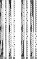
- Figure 3 shows the proposed design for SS/PBCH block pattern for sub-carrier spacings of 480 KHz and 960 KHz. This design enables harmonious operation of SS/PBCH blocks transmitted using 480 KHz and 960 KHz, while fully allowing the DL/UL control transmission opportunities for all SCS starting from 60 KHz. ⁇ ! ⁇ .
- Figure 3 shows one slot (14 symbols) at 60KHz SCS, which is equivalent in time to 28, 56, 112 and 224 symbols of 120 KHz, 240 KHz, 480 KHz and 960 KHz SCS respectively.
- the figure comprises of four sub-figures stacked on top of each other, where each sub-figure shows one slot (14 OFDM symbols) of 240 KHz SCS.
- the first 5 rows show the symbols from 60 KHz to 960 KHz SCS, with SCS mentioned in the first column.
- the first two symbols (0, 1, 14, 15, 28, 29, 42, 43, 56, 57, 70, 71, 84, 85, 98, 99) of each slot (14 OFDM symbols) have been highlighted to show the potential downlink control transmission
- the last two symbols (12, 13, 26, 27, 40, 41, 54, 55, 68, 69, 82, 83, 96, 97) have been highlighted to show potential uplink control transmissions which may occur in those symbols.
- the bottom part in each sub-figure provides a design of SS/PBCH block pattern for 480 KHz and 960 KHz SCSs.
- This design allocates first 20 SS/PBCH block candidate positions for 960 KHz SCS and first 10 candidate positions for 480 KHz in 250 micro-seconds.
- the pattern repeats itself in the upcoming intervals of 250 microseconds. If the number of candidate positions is restricted to 64, the last interval will only have 4 SS/PBCH block candidate positions. It is recommended to use the first 4 candidate positions in the last interval to accommodate the last 4 candidates to achieve overall 64 beams (requiring 64 SS/PBCH blocks) . With these repetitions employed, the 64 candidate positions will be finished within 1000 microseconds (4 slots of 60 KHz SCS) for 960 SCS and within 1750 microseconds (7 slots of 60 KHz SCS) for 480 KHz SCS SSB transmission.
- SS/PBCH positions may be defined with respect to the first symbol in a half-frame of 5 milliseconds.
- reference symbol index 0 corresponds to the first symbol of the first slot in a half-frame where SS/PBCH blocks are being transmitted.
- the first symbol indices for candidate SS/PBCH blocks are determined according to the SCS of SS/PBCH blocks as follows:
- n 0, 1, 2, 3, 4, 5, 6
- the reference symbol for SS/PBCH candidate positions can be taken to be a different reference than the first symbol of the half-frame. Similarly, if need be, for high frequency operation, the duration of the SS/PBCH burst can be reduced from 5 milliseconds.
- the SS/PBCH burst is designed such that the proposed SS/PBCH block candidate positions never overlap with any potential downlink control (1 st two OFDM symbols in the slot) and uplink control (last two OFDM symbols in the slot) for any SCS from 60 KHz to 480 KHz.
- the proposed SS/PBCH BLOCK pattern in this design for 480 KHz and 960 KHz allow complete downlink and uplink control resources when this control transmission may use any SCS from 60 KHz to 480 KHz.
- the proposed SS/PBCH BLOCK positions overlap for downlink control and uplink control when this control transmission is using the SCS of 960 KHz.
- downlink control first 2 symbols of the slot
- uplink control last 2 symbols of the slot
- only 25%of the positions may have the overlap with SS/PBCH BLOCK candidate positions when all SS/PBCH BLOCK candidate positions are utilised.
- Design 1 for the SS/PBCH burst packs the SS/PBCH candidate positions in a shortest possible interval while avoiding the overlap with DL and UL transmission opportunities.
- Design 1 though has some limitations: one issue with Design 1 is that it is not symmetric. As an example, in Design 1 for 480 KHz SCS with 64 candidates, first 6 intervals of 250 micro-seconds have 10 SS/PBCH candidate positions and the last interval has only 4 positions to achieve 64 candidate positions. The second issue is related to different SS/PBCH candidate density in time. For each set of two slots of 480 KHz, first set has 2, next 2 sets have 3 and the 4th set has 2 SS/PBCH candidate positions.
- This varying density of SS/PBCH candidate positions in different intervals will result in a complicated design for transmission of remaining minimum system information and will impose additional restrictions for the beam sweep based operation.
- this section proposes a novel SS/PBCH burst pattern.
- This design is constructed based upon the principles of packing SS/PBCH candidate positions as close as possible.
- the issues in Design 1 are additionally overcome by eliminating the SS/PBCH candidate positions in the 2nd and 3rd set, where each set spans 2 slots of 480 KHz. More precisely, single SS/PBCH candidate positions, 1 in 2nd set and 1 in 3rd set, are removed.
- Figure 4 shows this optimized design for SS/PBCH block pattern for sub-carrier spacings of 480 KHz and 960 KHz. This design enables harmonious operation of SS/PBCH candidates transmitted using 480 KHz and 960 KHz, with allowing fully the data transmission opportunities for all SCS starting from 60 KHz.
- Figure 4 shows one slot (14 symbols) of 60KHz SCS, which is equivalent in time to 28, 56, 112 and 224 symbols of 120 KHz, 240 KHz, 480 KHz and 960 KHz SCS respectively.
- the figure comprises of four sub-figures stacked on top of each other, where each sub-figure shows one slot (14 OFDM symbols) of 240 KHz SCS.
- first 5 rows show the symbols/slots from 60 KHz to 960 KHz SCS, with SCS mentioned in the first column.
- SCS for each SCS in its corresponding row, the first two symbols have been highlighted to show the potential downlink control transmission, and the last two symbols have been highlighted to show the potential uplink control transmission.
- the bottom part in each sub-figure provides the design of SS/PBCH BLOCK pattern for 480 KHz and 960 KHz SCSs.
- This design allocates first 16 SS/PBCH block candidate positions for 960 KHz SCS and first 8 candidate positions for 480 KHz in 250 microseconds.
- the pattern repeats itself in the subsequent intervals of 250 microseconds. If the number of candidate positions is restricted to 64, four periods of 250 micro-seconds will accommodate 64 SS/PBCH BLOCK candidate positions for SCS of 960 KHz which will finish in 1 millisecond. For 480 KHz SCS, one interval of 250 micro-seconds provides 8 candidate SS/PBCH BLOCK positions, thus 8 such intervals spanning 2 milliseconds will furnish 64 candidate SS/PBCH block positions.
- SS/PBCH positions may be defined with respect to the first symbol in a half-frame of 5 milliseconds.
- reference symbol index 0 corresponds to the first symbol of the first slot in a half-frame where SS/PBCH blocks are being transmitted.
- the first symbol indices for candidate SS/PBCH blocks are determined according to the SCS of SS/PBCH blocks as follows:
- n 0, 1, 2, 3, 4, 5, 6, 7
- n 0, 1, 2, ..., 15
- the SS/PBCH BLOCK pattern is designed such that the proposed SS/PBCH BLOCK candidate positions never overlap with any potential downlink control (1 st two OFDM symbols in the slot) and uplink control (last two OFDM symbols in the slot) for any SCS from 60 KHz to 480 KHz.
- the proposed SS/PBCH BLOCK pattern in this design for 480 KHz and 960 KHz allow complete downlink and uplink control resources when this control transmission may use any SCS from 60 KHz to 480 KHz.
- the proposed SS/PBCH BLOCK positions overlap though for downlink control and uplink control when this control transmission is using the SCS of 960 KHz.
- downlink control first 2 symbols of the slot
- uplink control last 2 symbols of the slot
- only 25%of the positions may have the overlap with SS/PBCH BLOCK candidate positions when all SS/PBCH BLOCK candidate positions are utilised.
- the proposed design in this section differs with respect to the first design in that 960 KHz SCS does not have 4 candidate positions starting at symbols 88, 92, 128 and 130, and 480 KHz SCS design does not have two SS/PBCH BLOCK candidate positions starting at symbols 44 and 64.
- the first design finishes the 64 candidate burst faster compared to the second design proposed in this section, the first design is asymmetric in the sense that the last interval of 250 micro seconds has different number of SS/PBCH BLOCK candidates than the first and intermediate intervals.
- the design proposed in this section is completely symmetric and all the intervals of 250 micro-seconds equally carry 16 or 8 SS/PBCH block candidate positions for 960 KHz or 480 KHz SCS respectively. This facilitates UE implementation and its search for synchronization block when it is trying to synchronize to a given cell.
- the proposed pattern can be easily extended by repeating the 250 micro-seconds interval multiple times. For 960 KHz SCS, as 250 micro-seconds period provides 16 SS/PBCH BLOCK candidate positions, the pattern repeated 8 and 16 times will furnish 128 and 256 positions respectively. For 480 KHz SCS, as 250 micro-seconds period provides 8 SS/PBCH BLOCK candidate positions, the pattern repeated 16 and 32 times will furnish 128 and 256 positions respectively.
- a very important aspect of this design is that the proposed design for SS/PBCH block transmissions for 480 KHz SCS and 960 KHz SCS combined with existing designs for 120 KHz SCS and 240 KHz SCS provide SS/PBCH BLOCK design for 4 different SCSs which harmoniously integrate with control/data transmissions from 60 KHz SCS up to 960 KHz SCS. This allows easy projection to even higher SCS if need be.
- all the SCS in Figure 4 can be projected to next level, 960 KHz SCS becoming 1920 KHz, 480 KHz becoming 960 KHz and same for all, the same patterns as shown in the figure can be re-used with this change of notation for SCS and they will provide the SS/PBCH patterns from 240 KHz SCS to 1960 KHz SCS, still having the nice properties of minimal or no overlap with DL and UL control.
- all the SCS in this design can be scaled to two level up or a different higher level, and will instantly provide the SS/PBCH block design for higher SCS with nice properties.
- Figure 5 shows a third design for SS/PBCH block transmission pattern for sub-carrier spacings of 480 KHz and 960 KHz.
- the underlying principle behind this design is to re-use the SS/PBCH burst design for 120 KHz and 240 KHz SCS.
- the designs of 120 KHz and 240 KHz SCS are re-used for 480 KHz and 960 KHz SCS.
- ⁇ ! ⁇ . shows one slot (14 symbols) of 60KHz SCS, which is equivalent in time to 28, 56, 112 and 224 symbols of 120 KHz, 240 KHz, 480 KHz and 960 KHz SCS respectively.
- the figure comprises of four sub-figures vertically, each showing one slot of 240 KHz SCS.
- the design proposed in this section basically scales the 3GPP Release-15 SS/PBCH block pattern design for 120 KHz and 240 KHz SCS to 480 KHz and 960 SCS.
- the legacy design was made to function with control and data SCS of 60 and 120 KHz
- the proposed scalable design works very well when control and data are transmitted using SCS of 240 KHz or beyond (480 KHz, 960 KHz) .
- the figure shows that there are significant overlapping DL/UL control occasions for lower SCS of 60 KHz, 120 KHz and 240 KHz.
- the use of this design when all of these SCS can be used may impose certain restrictions.
- the overlap occurs at 50%of occasions, i.e., half of the DL control (first 2 symbols of the slot) and half of the UL control (last 2 symbols of the slot) are not available when all the candidate SS/PBCH BLOCK positions are occupied to transmit SS/PBCH BLOCK.
- this design packs the SS/PBCH candidate positions in a very short interval, this impact of overlapping control positions for 960 KHz SCS can be acceptable.
- a frequency carrier either uses SCS 60 to 240 KHz, or 240 KHz to 960 KHz for its operation including SS/PBCH transmission and DL/UL control and data transmission.
- SS/PBCH positions may be defined with respect to the first symbol in a half-frame of 5 milliseconds.
- reference symbol index 0 corresponds to the first symbol of the first slot in a half-frame where SS/PBCH blocks are being transmitted.
- the first symbol indices for candidate SS/PBCH blocks are determined according to the SCS of SS/PBCH blocks as follows:
- n 0, 1, 2, 3, 4, 5, 6, 7
- n 0, 1, 2, ..., 15
- the SS/PBCH BLOCK candidates are packed in a very short span of time.
- 64 SS/PBCH BLOCK candidate positions are filled in 32 slots of SCS of SS/PBCH block, which spans a time of 500 microseconds at SCS of 960 KHz or a time of 1 millisecond for 480 KHz SCS.
- this will leave a big fraction of slots where no SS/PBCH BLOCK need to be transmitted and thus those slots can be fully utilized for scheduling, control and data transmission.
- This design is more suitable to be used for 480 KHz or 960 KHz SS/PBCH BLOCK, if the control/data use 240 KHz SCS or higher.
- the design can be very advantageous if control/data are restricted to use a SCS of 240 KHz and higher.
- This disclosure has proposed designs for high frequency operation with very large SCS of 480 KHz and 960 KHz.
- the beam switching delays are only a small fraction of symbol time. So if there are some transients due to beam switching, they will only be present over a fraction of the boundary symbol (s) and may be acceptable.
- the symbol durations are very short, of the order of few micro seconds.
- the beam switching delays may become an important issue and the associated transients may prevail over a significant portion of the symbol. This will imply that the SS/PBCH blocks placed back-to-back for different beams may potentially degrade the synchronization quality.
- This figure shows one slot (14 OS) of 60 KHz SCS, which is split in 4 sub-figures stacked vertically, with each showing one slot of 240 KHz SCS.
- Each sub-figure shows the DL/UL control symbols for 60 KHz to 960 KHz SCSs.
- the last three rows in each figure are the gap based SS/PBCH block patterns for 960 KHz SCS.
- n 0, 1, 2, 3, 4
- n 0, 1, 2, ..., 10
- D3-960KHz-2OS gap is derived from the underlying principle of design D3, by introducing suitably at least 2 OFDM symbols (OS) between the consecutive SS/PBCH blocks.
- This design as of its parent design D3, is more suitable when the control and data are using the SCS of 240 KHz and beyond.
- the first symbol positions for the SS/PBCH block candidates for this design can be represented as in the following:
- n 0, 1, 2, 3, 4, 5, 6, 7, 8, 9, 10
- the proposed designs have been mainly proposed for 480 KHz SCS and 960 KHz SCS, though these SCS can be easily scaled up further keeping the same SS/PBCH block patterns. Scaling to higher SCS keeping the same design will shrink the patterns in time due to shortening of symbol intervals, though it will retain the features of the proposed design. This will allow easy extension of the proposed designs to a wide variety of SCS. To avoid overlap with DL/UL control occasions of very low SCS, some of the lower SCS may be restricted to be used for control/data transmissions.
- one strategy can be to limit a set of SCS for data and SS/PBCH transmission.
- One set can be 60 KHz to 240 KHz which will allow data and SS/PBCH transmission within this set.
- one or two additional sets can be formed.
- Each restricted set can have the SS/PBCHs which have no or minimal overlap within this set.
- This design strategy can then enable the application of Design 3 to any of the sets formed.
- the UE synchronization can be facilitated by defining one default SCS for SS/PBCH transmission for each frequency set.
- Another design for higher SCS SS/PBCH candidates is to place the SS/PBCH candidates of higher SCS (say 1920 KHz) on the positions which are occupied in current designs. As 1920 KHz has double the number of symbols compared to 960 KHz for a given time duration, the SS/PBCH positions get doubled. Out of these indices, candidate positions overlapping with lower SCS control can be removed and first 64 (or desired number) of positions can be kept.
- 3GPP NR Release-15 has restricted the burst length to duration of half-frame, i.e., 5 milliseconds. This basically means that all the candidate positions for a given frequency range always fit within this duration of 5 milliseconds.
- the proposed designs in this disclosure provide the symbols positions from a reference symbol 0. To keep up with the existing design, this reference symbol 0 is taken to be the first symbol of the half-frame. Nevertheless, for higher frequency operation, the symbol times will become very small with the use of very large SCS. This may lead to the change of burst length from 5 milliseconds to smaller time intervals. The proposed designs stay valid even if the burst length is changed to a different duration.
- the symbol 0, the reference point, in the proposed designs need to be mapped to the new reference symbol as a minor adaptation to achieve the designs for any new burst duration.
- the proposed designs have provided 64 candidate positions where currently 3GPP has decided to support up to 64 beams in FR2 and FR2-extensions going up to 71 GHz.
- the readers will appreciate though that the three proposed designs can be easily adapted to achieve smaller or larger number of SS/PBCH candidate positions.
- To achieve smaller number of beam positions say 32 or 16, first 32 or 16 candidate positions in the proposed design can be used.
- the SS/PBCH block can only be defined for 960 KHz, which then also becomes the SCS of choice for high frequency operation. In such a case, depending upon which frequencies are allowed for control/data transmission, any suitable 960 KHz SCS SS/PBCH block pattern can be selected from the proposed designs.
- SS/PBCH block transmission patterns for SCS of 480 KHz and 960 KHz allowing no or minimal overlap with DL and UL control.
- Proposed patterns are easily scalable to further higher SCS, employing the proposed guidelines.
- any of the devices or apparatus that form part of the network may include at least a processor, a storage unit and a communications interface, wherein the processor unit, storage unit, and communications interface are configured to perform the method of any aspect of the present invention. Further options and choices are described below.
- the signal processing functionality of the embodiments of the invention especially the gNB and the UE may be achieved using computing systems or architectures known to those who are skilled in the relevant art.
- Computing systems such as, a desktop, laptop or notebook computer, hand-held computing device (PDA, cell phone, palmtop, etc. ) , mainframe, server, client, or any other type of special or general purpose computing device as may be desirable or appropriate for a given application or environment can be used.
- the computing system can include one or more processors which can be implemented using a general or special-purpose processing engine such as, for example, a microprocessor, microcontroller or other control module.
- the computing system can also include a main memory, such as random access memory (RAM) or other dynamic memory, for storing information and instructions to be executed by a processor. Such a main memory also may be used for storing temporary variables or other intermediate information during execution of instructions to be executed by the processor.
- the computing system may likewise include a read only memory (ROM) or other static storage device for storing static information and instructions for a processor.
- ROM read only memory
- the computing system may also include an information storage system which may include, for example, a media drive and a removable storage interface.
- the media drive may include a drive or other mechanism to support fixed or removable storage media, such as a hard disk drive, a floppy disk drive, a magnetic tape drive, an optical disk drive, a compact disc (CD) or digital video drive (DVD) (RTM) read or write drive (R or RW) , or other removable or fixed media drive.
- Storage media may include, for example, a hard disk, floppy disk, magnetic tape, optical disk, CD or DVD, or other fixed or removable medium that is read by and written to by media drive.
- the storage media may include a computer-readable storage medium having particular computer software or data stored therein.
- an information storage system may include other similar components for allowing computer programs or other instructions or data to be loaded into the computing system.
- Such components may include, for example, a removable storage unit and an interface , such as a program cartridge and cartridge interface, a removable memory (for example, a flash memory or other removable memory module) and memory slot, and other removable storage units and interfaces that allow software and data to be transferred from the removable storage unit to computing system.
- the computing system can also include a communications interface.
- a communications interface can be used to allow software and data to be transferred between a computing system and external devices.
- Examples of communications interfaces can include a modem, a network interface (such as an Ethernet or other NIC card) , a communications port (such as for example, a universal serial bus (USB) port) , a PCMCIA slot and card, etc.
- Software and data transferred via a communications interface are in the form of signals which can be electronic, electromagnetic, and optical or other signals capable of being received by a communications interface medium.
- computer program product may be used generally to refer to tangible media such as, for example, a memory, storage device, or storage unit.
- These and other forms of computer-readable media may store one or more instructions for use by the processor comprising the computer system to cause the processor to perform specified operations.
- Such instructions generally 45 referred to as ‘computer program code’ (which may be grouped in the form of computer programs or other groupings) , when executed, enable the computing system to perform functions of embodiments of the present invention.
- the code may directly cause a processor to perform specified operations, be compiled to do so, and/or be combined with other software, hardware, and/or firmware elements (e.g., libraries for performing standard functions) to do so.
- the non-transitory computer readable medium may comprise at least one from a group consisting of: a hard disk, a CD-ROM, an optical storage device, a magnetic storage device, a Read Only Memory, a Programmable Read Only Memory, an Erasable Programmable Read Only Memory, EPROM, an Electrically Erasable Programmable Read Only Memory and a Flash memory.
- the software may be stored in a computer-readable medium and loaded into computing system using, for example, removable storage drive.
- a control module (in this example, software instructions or executable computer program code) , when executed by the processor in the computer system, causes a processor to perform the functions of the invention as described herein.
- inventive concept can be applied to any circuit for performing signal processing functionality within a network element. It is further envisaged that, for example, a semiconductor manufacturer may employ the inventive concept in a design of a stand-alone device, such as a microcontroller of a digital signal processor (DSP) , or application-specific integrated circuit (ASIC) and/or any other sub-system element.
- DSP digital signal processor
- ASIC application-specific integrated circuit
- aspects of the invention may be implemented in any suitable form including hardware, software, firmware or any combination of these.
- the invention may optionally be implemented, at least partly, as computer software running on one or more data processors and/or digital signal processors or configurable module components such as FPGA devices.
- an embodiment of the invention may be physically, functionally and logically implemented in any suitable way. Indeed, the functionality may be implemented in a single unit, in a plurality of units or as part of other functional units.
- the present invention has been described in connection with some embodiments, it is not intended to be limited to the specific form set forth herein. Rather, the scope of the present invention is limited only by the accompanying claims. Additionally, although a feature may appear to be described in connection with particular embodiments, one skilled in the art would recognise that various features of the described embodiments may be combined in accordance with the invention. In the claims, the term ‘comprising’ does not exclude the presence of other elements or steps.
Landscapes
- Engineering & Computer Science (AREA)
- Computer Networks & Wireless Communication (AREA)
- Signal Processing (AREA)
- Physics & Mathematics (AREA)
- Mathematical Physics (AREA)
- Mobile Radio Communication Systems (AREA)
Abstract
Des motifs de transmission pour des salves SS/PBCH sont décrits pour être utilisés à des valeurs SCS élevées afin d'atténuer le chevauchement entre des régions de signalisation de commande dans des motifs de transmission pour des valeurs SCS inférieures. Un procédé de transmission d'une salve SS/PBCH dans un système de transmission OFDM fonctionnant avec un espacement de sous-porteuse de 960 kHz comprend les étapes consistant à : sélectionner un emplacement de départ pour chacune d'une série de salves SS/PBCH, chaque salve ayant une durée d'au moins 2 symboles OFDM, les emplacements de départ étant sélectionnés de telle sorte que chaque salve ne chevauche pas les régions de transmission de commande de liaison montante ou de liaison descendante attribuées pour des espacements de sous-porteuses de 60 kHz, 120 kHz, 240 kHz, et 480 kHz; et la transmission d'une série de salves SS/PBCH, chaque salve commençant à l'un des emplacements de départ sélectionnés et ayant une durée permettant d'éviter un chevauchement avec des régions de transmission de commande de liaison montante ou de liaison descendante attribuées pour des espacements de sous-porteuses de 60 kHz, 120 kHz, 240 kHz et 480 kHz.
Priority Applications (1)
| Application Number | Priority Date | Filing Date | Title |
|---|---|---|---|
| CN202180049594.3A CN115804166A (zh) | 2020-07-17 | 2021-07-16 | 蜂窝通信系统中的传输模式 |
Applications Claiming Priority (2)
| Application Number | Priority Date | Filing Date | Title |
|---|---|---|---|
| US202063053390P | 2020-07-17 | 2020-07-17 | |
| US63/053,390 | 2020-07-17 |
Publications (1)
| Publication Number | Publication Date |
|---|---|
| WO2022012686A1 true WO2022012686A1 (fr) | 2022-01-20 |
Family
ID=79554502
Family Applications (1)
| Application Number | Title | Priority Date | Filing Date |
|---|---|---|---|
| PCT/CN2021/106922 Ceased WO2022012686A1 (fr) | 2020-07-17 | 2021-07-16 | Motifs de transmission dans des systèmes de communication cellulaire |
Country Status (2)
| Country | Link |
|---|---|
| CN (1) | CN115804166A (fr) |
| WO (1) | WO2022012686A1 (fr) |
Citations (2)
| Publication number | Priority date | Publication date | Assignee | Title |
|---|---|---|---|---|
| WO2018237032A1 (fr) * | 2017-06-21 | 2018-12-27 | Intel Corporation | Traitement de collision de blocs de signaux de synchronisation (ss) |
| CN110583054A (zh) * | 2017-05-04 | 2019-12-17 | Oppo广东移动通信有限公司 | 同步信号块的定时方法及相关产品 |
Family Cites Families (4)
| Publication number | Priority date | Publication date | Assignee | Title |
|---|---|---|---|---|
| US10362610B2 (en) * | 2016-09-19 | 2019-07-23 | Samsung Electronics Co., Ltd. | Method and apparatus for mapping initial access signals in wireless systems |
| AU2018283571B2 (en) * | 2017-06-15 | 2020-07-09 | Lg Electronics Inc. | Method for transmitting and receiving synchronization signal block and device therefor |
| US10462761B2 (en) * | 2017-07-25 | 2019-10-29 | Samsung Electronics Co., Ltd. | Method and SS block time locations and SS burst set composition for NR unlicensed spectrum |
| US10849110B2 (en) * | 2018-02-16 | 2020-11-24 | Qualcomm Incorporated | Resource allocation for the physical uplink control channel |
-
2021
- 2021-07-16 WO PCT/CN2021/106922 patent/WO2022012686A1/fr not_active Ceased
- 2021-07-16 CN CN202180049594.3A patent/CN115804166A/zh active Pending
Patent Citations (2)
| Publication number | Priority date | Publication date | Assignee | Title |
|---|---|---|---|---|
| CN110583054A (zh) * | 2017-05-04 | 2019-12-17 | Oppo广东移动通信有限公司 | 同步信号块的定时方法及相关产品 |
| WO2018237032A1 (fr) * | 2017-06-21 | 2018-12-27 | Intel Corporation | Traitement de collision de blocs de signaux de synchronisation (ss) |
Non-Patent Citations (2)
| Title |
|---|
| LG ELECTRONICS: "Remaining issues on SS block design and indication method", 3GPP DRAFT; R1-1713121 REMAINING ISSUES ON SS BLOCK DESIGN AND INDICATION METHOD, vol. RAN WG1, 20 August 2017 (2017-08-20), Prague, Czech Republic, pages 1 - 8, XP051315930 * |
| SAMSUNG: "SS burst set composition", 3GPP DRAFT; R1-1711580 SS BURST SET COMPOSITION V2, vol. RAN WG1, 27 June 2017 (2017-06-27), Qingdao, P.R. China, pages 1 - 6, XP051305893 * |
Also Published As
| Publication number | Publication date |
|---|---|
| CN115804166A (zh) | 2023-03-14 |
Similar Documents
| Publication | Publication Date | Title |
|---|---|---|
| US20210377938A1 (en) | Frequency domain allocation techniques | |
| US20240298316A1 (en) | Mobile station, base station, transmission method and reception method | |
| EP3905842A1 (fr) | Procédé exécuté par un équipement utilisateur, et équipement utilisateur | |
| EP2225908B1 (fr) | Signalisation d'accès aléatoire efficace basée sur une expression de l'attribution d'un premier ressource d'accès aléatoire à utiliser par rapport à une sous-trame de liaison montante | |
| US9060304B2 (en) | Radio frame and sounding reference signal sending method in mobile communication system | |
| US8050223B2 (en) | System and method for facilitating co-channel and co-existence via enhanced frame preambles | |
| US8780769B2 (en) | Method, apparatus, and system for identifying different frame structures | |
| EP3863204B1 (fr) | Procédé d'émission de signal de synchronisation, appareil de réseau et appareil terminal | |
| EP3751944A1 (fr) | Dispositif et procédé de transmission de préambule d'accès aléatoire | |
| US12309015B2 (en) | Synchronization signal transmission | |
| JP6740415B2 (ja) | ライセンス不要アクセスについてのプリアンブルについての装置、システム、及び方法 | |
| CN111316748B (zh) | 减少新无线电中被寻呼用户设备的随机接入的或与之相关的改进 | |
| US11070331B2 (en) | Communication device for LTE communication within unused GSM channels | |
| US12022522B2 (en) | Method for transmitting and receiving discovery reference signal, and device for same | |
| KR20190132380A (ko) | 정보를 전송하는 방법, 단말 장비 및 네트워크 장비 | |
| EP3477883B1 (fr) | Procédé et dispositif pour configurer et acquérir des paramètres de transmission d'une couche physique | |
| EP3138349B1 (fr) | Schéma de canal prach amélioré pour des économies d'énergie, une amélioration de la portée et une détection améliorée | |
| WO2018082527A1 (fr) | Systèmes et procédés d'attribution de ressources sans fil | |
| WO2022017522A1 (fr) | Transmission efficace d'informations système | |
| US12432783B2 (en) | Physical random access channel enhancements in new radio | |
| EP4099743A1 (fr) | Terminal et station de base | |
| WO2022012686A1 (fr) | Motifs de transmission dans des systèmes de communication cellulaire | |
| EP4686132A1 (fr) | Procédé et appareil de communication | |
| JP2021521669A (ja) | クリアチャネルのリスニング方法、装置及び機器 | |
| WO2022012643A1 (fr) | Signaux de synchronisation dans un spectre partagé pour réseaux cellulaires |
Legal Events
| Date | Code | Title | Description |
|---|---|---|---|
| 121 | Ep: the epo has been informed by wipo that ep was designated in this application |
Ref document number: 21842550 Country of ref document: EP Kind code of ref document: A1 |
|
| NENP | Non-entry into the national phase |
Ref country code: DE |
|
| 122 | Ep: pct application non-entry in european phase |
Ref document number: 21842550 Country of ref document: EP Kind code of ref document: A1 |