WO2022085247A1 - Élément optique à cristaux liquides - Google Patents
Élément optique à cristaux liquides Download PDFInfo
- Publication number
- WO2022085247A1 WO2022085247A1 PCT/JP2021/025455 JP2021025455W WO2022085247A1 WO 2022085247 A1 WO2022085247 A1 WO 2022085247A1 JP 2021025455 W JP2021025455 W JP 2021025455W WO 2022085247 A1 WO2022085247 A1 WO 2022085247A1
- Authority
- WO
- WIPO (PCT)
- Prior art keywords
- liquid crystal
- alignment film
- optical element
- substrate
- orientation direction
- Prior art date
- Legal status (The legal status is an assumption and is not a legal conclusion. Google has not performed a legal analysis and makes no representation as to the accuracy of the status listed.)
- Ceased
Links
Images



Classifications
-
- G—PHYSICS
- G02—OPTICS
- G02B—OPTICAL ELEMENTS, SYSTEMS OR APPARATUS
- G02B5/00—Optical elements other than lenses
- G02B5/18—Diffraction gratings
- G02B5/1833—Diffraction gratings comprising birefringent materials
-
- G—PHYSICS
- G02—OPTICS
- G02B—OPTICAL ELEMENTS, SYSTEMS OR APPARATUS
- G02B5/00—Optical elements other than lenses
- G02B5/18—Diffraction gratings
-
- G—PHYSICS
- G02—OPTICS
- G02B—OPTICAL ELEMENTS, SYSTEMS OR APPARATUS
- G02B5/00—Optical elements other than lenses
- G02B5/30—Polarising elements
-
- G—PHYSICS
- G02—OPTICS
- G02B—OPTICAL ELEMENTS, SYSTEMS OR APPARATUS
- G02B5/00—Optical elements other than lenses
- G02B5/30—Polarising elements
- G02B5/3016—Polarising elements involving passive liquid crystal elements
-
- G—PHYSICS
- G02—OPTICS
- G02B—OPTICAL ELEMENTS, SYSTEMS OR APPARATUS
- G02B5/00—Optical elements other than lenses
- G02B5/20—Filters
- G02B5/208—Filters for use with infrared or ultraviolet radiation, e.g. for separating visible light from infrared and/or ultraviolet radiation
Definitions
- the embodiment of the present invention relates to a liquid crystal optical element.
- a liquid crystal polarizing grid using a liquid crystal material divides the incident light into 0th-order diffracted light and 1st-order diffracted light when light having a wavelength ⁇ is incident.
- the refractive index anisotropy or birefringence ⁇ n difference between the refractive index ne for abnormal light and the refractive index no for normal light
- An object of the present embodiment is to provide a liquid crystal optical element capable of obtaining desired optical performance.
- the liquid crystal optical element of this embodiment is Between the substrate having the first main surface, the first alignment film arranged on the first main surface, the second alignment film facing the first alignment film, and the substrate and the second alignment film.
- a plurality of first liquid crystals arranged along a boundary surface with the first alignment film are provided with an arranged spacer and a liquid crystal layer in contact with the first alignment film and the second alignment film. It has a liquid crystal molecule containing a plurality of second liquid crystal molecules arranged along a boundary surface between the molecule and the second alignment film, and is cured in a state where the orientation direction of the liquid crystal molecule is fixed.
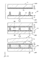
- FIG. 1 is a cross-sectional view schematically showing a liquid crystal optical element 1 according to the present embodiment.
- FIG. 2 is a diagram for explaining an example of a method for manufacturing the liquid crystal optical element 1 shown in FIG.
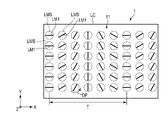
- FIG. 3 is a plan view schematically showing an example of the orientation pattern in the liquid crystal layer LC.
- FIG. 4 is a plan view schematically showing another example of the orientation pattern in the liquid crystal layer LC.
- FIG. 5 is a cross-sectional view schematically showing a first configuration example of the liquid crystal optical element 1.
- FIG. 6 is a cross-sectional view schematically showing a second configuration example of the liquid crystal optical element 1.
- FIG. 7 is a cross-sectional view schematically showing a third configuration example of the liquid crystal optical element 1.
- FIG. 8 is a cross-sectional view schematically showing a fourth configuration example of the liquid crystal optical element 1.
- the X-axis, Y-axis, and Z-axis that are orthogonal to each other are described as necessary for facilitating understanding.
- the direction along the Z axis is referred to as the Z direction or the first direction
- the direction along the Y axis is referred to as the Y direction or the second direction
- the direction along the X axis is referred to as the X direction or the third direction.
- the plane defined by the X-axis and the Y-axis is referred to as an XY plane.
- FIG. 1 is a cross-sectional view schematically showing the liquid crystal optical element 1 according to the present embodiment.
- the liquid crystal optical element 1 includes a substrate 10, a first alignment film AL1, a second alignment film AL2, a spacer SP, a liquid crystal layer LC, and a thin film 20.
- the substrate 10 is a transparent substrate that transmits light, and is composed of, for example, a transparent glass plate or a transparent synthetic resin plate.
- the substrate 10 may be made of, for example, a flexible transparent synthetic resin plate.
- the substrate 10 can take any shape.
- the substrate 10 may be curved.
- the refractive index of the substrate 10 is, for example, larger than the refractive index of air.
- light includes visible and invisible light.
- the lower limit wavelength of the visible light region is 360 nm or more and 400 nm or less
- the upper limit wavelength of the visible light region is 760 nm or more and 830 nm or less.
- Visible light has a first component (blue component) in the first wavelength band (for example, 400 nm to 500 nm), a second component (green component) in the second wavelength band (for example, 500 nm to 600 nm), and a third wavelength band (for example). It contains a third component (red component) of 600 nm to 700 nm).
- the invisible light includes ultraviolet rays in a wavelength band shorter than the first wavelength band and infrared rays in a wavelength band longer than the third wavelength band.
- transparent is preferably colorless and transparent. However, “transparent” may be translucent or colored transparent.
- the substrate 10 is formed in a flat plate shape along an XY plane, and has a first main surface F1 and a second main surface F2.
- the first main surface F1 and the second main surface F2 are planes substantially parallel to the XY plane and face each other in the Z direction.
- the second main surface F2 is in contact with air, for example, but may be covered with another thin film.
- the first alignment film AL1 is arranged on the first main surface F1 of the substrate 10. In the example shown in FIG. 1, the first alignment film AL1 is in contact with the substrate 10. In addition, another thin film may be interposed between the first alignment film AL1 and the substrate 10.
- the first alignment film AL1 is formed of, for example, polyimide.
- the second alignment film AL2 faces the first alignment film AL1 in the Z direction.
- the second alignment film AL2 may be formed of the same material as the first alignment film AL1, or may be formed of a material different from that of the first alignment film AL1.
- Both the first alignment film AL1 and the second alignment film AL2 are horizontal alignment films having an orientation regulating force along the XY plane.
- the anchoring strength in the present specification indicates the magnitude of the orientation regulating force, and corresponds to the so-called azimuth angle anchoring strength. Such anchoring strength represents the magnitude of the interaction between the alignment film and the liquid crystal molecules, and is simply referred to as "anchoring strength of the alignment film". It is desirable that the anchoring strength of the second alignment film AL2 is smaller than the anchoring strength of the first alignment film AL1. In one example, the anchoring strength of the first alignment film AL1 is 1 * 10 -4 J / m 2 or more, and the anchoring strength of the second alignment film AL2 is 1 * 10 -6 J / m 2 or less. .. The anchoring strength of the first alignment film AL1 and the second alignment film AL2 may be 1 * 10 -4 J / m 2 or more.
- the spacer SP is arranged between the substrate 10 and the second alignment film AL2 in the Z direction.
- the spacer SP may be a columnar spacer extending in the Z direction, or may be a substantially spherical bead.
- the spacer SP is preferably transparent.
- the spacer SP is formed in a columnar shape, for example, in a step after the first alignment film AL1 is formed. In this case, as shown in FIG. 1, the spacer SP overlaps the first alignment film AL1 in the Z direction and is arranged between the first alignment film AL1 and the second alignment film AL2. Further, the spacer SP is in contact with the first alignment film AL1 and the second alignment film AL2.
- the spacer SP may be formed in a step prior to the first alignment film AL1.
- the spacer SP is formed so as to be in contact with the first main surface F1 and is arranged between the substrate 10 and the second alignment film AL2 in the Z direction.
- the first alignment film AL1 is formed so as to cover at least a part of the spacer SP.
- the spacer SP may be in contact with the second alignment film AL2, or the first alignment film AL1 may intervene between the spacer SP and the second alignment film AL2.
- the liquid crystal layer LC is arranged between the first alignment film AL1 and the second alignment film AL2, and is in contact with the first alignment film AL1 and the second alignment film AL2.
- the thickness d of the liquid crystal layer LC along the Z direction is equivalent to the thickness T1 of the spacer SP.
- the liquid crystal layer LC is not interposed between the spacer SP and the second alignment film AL2.
- the liquid crystal layer LC has a plurality of liquid crystal structures LMS having different orientation directions from each other.
- the plurality of liquid crystal structures LMS can take a linear orientation pattern or a non-linear alignment pattern.
- the linear orientation pattern shows a pattern in which the orientation direction of a plurality of liquid crystal structures LMS changes linearly.
- Linear change means, for example, that the amount of change in the orientation direction of the liquid crystal structure LMS is represented by a linear function.
- the non-linear orientation pattern shows a pattern in which the orientation direction of a plurality of liquid crystal structures LMS changes non-linearly.
- “Nonlinear change” means, for example, that the amount of change in the orientation direction of the liquid crystal structure LMS is expressed by an Nth-order function. "N” indicates an integer of 2 or more.
- the liquid crystal structure LMS has a first liquid crystal molecule LM1 located on one end side thereof and a second liquid crystal molecule LM2 located on the other end side.
- the first liquid crystal molecule LM1 is in close proximity to the first alignment film AL1
- the second liquid crystal molecule LM2 is in close proximity to the second alignment film AL2.
- a plurality of liquid crystal molecules including the first liquid crystal molecule LM1 and the second liquid crystal molecule LM2 in each liquid crystal structure LMS are arranged in the Z direction, and each liquid crystal molecule is oriented in a predetermined direction in the XY plane.
- the orientation direction of the second liquid crystal molecule LM2 changes linearly or non-linearly.
- the amount of change in the orientation direction of the first liquid crystal molecule LM1 and the amount of change in the orientation direction of the second liquid crystal molecule LM2 are expressed by an Nth-order function when N is an integer of 1 or more.
- N is 1 corresponds to the case where the orientation direction changes linearly
- the case where N is 2 or more corresponds to the case where the orientation direction changes non-linearly.
- the orientation direction of the liquid crystal molecules can be expressed as, for example, the angle ⁇ L formed by the major axis and the X axis of the liquid crystal molecules oriented in the XY plane.
- the amount of change in the orientation direction of the first liquid crystal molecule LM1 is the difference in the orientation direction of each of the first liquid crystal molecules LM1 of the two liquid crystal structures LMS arranged at a pitch corresponding to the unit length L, that is, the unit length. It can be expressed as the difference in the per-angle ( ⁇ L / L).
- the amount of change in the orientation direction of the two liquid crystal molecules LM2 can be expressed as the difference in the orientation direction of each of the second liquid crystal molecules LM2 of the two liquid crystal structures LMS arranged at a pitch corresponding to the unit length L. can.
- the liquid crystal layer LC of the present embodiment is cured in a state where the orientation direction of the liquid crystal molecules including the first liquid crystal molecule LM1 and the second liquid crystal molecule LM2 is fixed. That is, the orientation direction of the liquid crystal molecules is not controlled according to the electric field. Therefore, the liquid crystal optical element 1 does not have an electrode for orientation control.
- Such a liquid crystal layer LC is formed, for example, by applying energy such as light to a monomer to polymerize it.
- the thin film 20 overlaps the second alignment film AL2 in the Z direction. That is, the second alignment film AL2 is located between the liquid crystal layer LC and the thin film 20, and between the spacer SP and the thin film 20, respectively.
- the thin film 20 is transparent and is, for example, a polyimide-based organic film, but may be an inorganic film.
- the film thickness T2 along the Z direction of the thin film 20 is thicker than the film thickness T3 of the second alignment film AL2. No other thin film or substrate overlaps the thin film 20 in the Z direction. That is, the thin film 20 has a main surface F3 in contact with air.
- FIG. 2 is a diagram for explaining an example of the manufacturing method of the liquid crystal optical element 1 shown in FIG.
- the first substrate SUB1 and the second substrate SUB2 are prepared.
- the first substrate SUB1 is formed, for example, as follows.
- a case where the spacer SP is formed before the first alignment film AL1 will be described.
- a columnar spacer SP is formed on the first main surface F1 of the substrate 10 by using a transparent organic material.
- the alignment film material is applied to the first main surface F1 and the surface of the alignment film material is oriented to form the first alignment film AL1.
- the alignment treatment is, for example, a photo-alignment treatment, but other methods may be used.
- the alignment restricting force of the first alignment film AL1 is adjusted by the alignment treatment so as to have a predetermined anchoring strength as described above.
- the second substrate SUB2 is formed, for example, as follows. First, a support substrate 30 having facing main surfaces F4 and F5 is prepared. The support substrate 30 is, for example, a glass substrate. After that, a polyimide-based thin film 20 is formed on the main surface F4 of the support substrate 30. Then, the alignment film material is applied over the thin film 20 to form the second alignment film AL2.
- a second alignment film AL2 has an orientation regulating force that at least exhibits horizontal orientation, but the anchoring strength of the second alignment film AL2 is weak as described above.
- step ST2 the first substrate SUB1 and the second substrate SUB2 are bonded together, and the liquid crystal layer LC is formed.
- the liquid crystal layer LC is formed, for example, as follows. First, the liquid crystal material is applied so as to be in contact with the first alignment film AL1. After that, the second substrate SUB2 is superposed so that the second alignment film AL2 is in contact with the liquid crystal material. The second substrate SUB2 is supported by the spacer SP. Then, the liquid crystal material is cured by irradiating it with light such as ultraviolet rays to form a liquid crystal layer LC.
- each of the first liquid crystal molecules LM1 close to the first alignment film AL1 is horizontally oriented along the XY plane by the orientation restricting force of the first alignment film AL1, and is oriented in a predetermined direction on the XY plane. Oriented to.
- the orientation direction of the liquid crystal molecule overlapping in the Z direction with respect to the first liquid crystal molecule LM1 is determined according to the orientation direction of the first liquid crystal molecule LM1.
- the second liquid crystal molecule LM2 close to the second alignment film AL2 is horizontally aligned along the XY plane due to the orientation restricting force of the second alignment film AL2.
- the anchoring strength of the second alignment film AL2 is weak, the degree of freedom is high with respect to the orientation direction of the second liquid crystal molecule LM2 in the XY plane. Therefore, the second liquid crystal molecule LM2 is oriented so as to follow the orientation direction of the first liquid crystal molecule LM1.
- the support substrate 30 is peeled off.
- laser lift-off can be applied. That is, by irradiating the main surface F5 of the support substrate 30 with high-power laser light (for example, laser light having an ultraviolet wavelength) to heat and decompose the interface between the thin film 20 and the support substrate 30, the thin film 20 is subjected to the support substrate. 30 is peeled off. That is, the thin film 20 in the present embodiment functions as a release agent that absorbs light having a predetermined wavelength to promote the release of the support substrate 30 (or reduce the degree of adhesion to the support substrate 30). It should be noted that part or all of the thin film 20 may be removed as the support substrate 30 is peeled off. The surface of the thin film 20 remaining after the support substrate 30 is peeled off forms a main surface F3 in contact with air. When the entire thin film 20 is removed, the second alignment film AL2 is exposed and comes into contact with air.
- high-power laser light for example, laser light having an ultraviolet wavelength
- the orientation direction of the liquid crystal molecules contained in the applied liquid crystal material is mainly due to the orientation restricting force of the first alignment film AL1 provided on the first substrate SUB1. It will be decided.
- the orientation restricting force of the second alignment film AL2 provided on the second substrate SUB2 suppresses the rise of the second liquid crystal molecule LM2 (a state approaching vertical alignment) in the vicinity of the second alignment film AL2.
- the desired refractive index anisotropy ⁇ n can be obtained in the cured liquid crystal layer LC.
- the spacer SP is provided on the liquid crystal layer LC, the bending of the first substrate SUB1 and the second substrate SUB2 to be bonded in the process of forming the liquid crystal layer LC is suppressed. As a result, the gap between the first substrate SUB1 and the second substrate SUB2 along the Z direction is made uniform. Therefore, the thickness d of the cured liquid crystal layer LC can be made uniform.
- the liquid crystal optical element 1 in which the liquid crystal layer LC is configured to have a predetermined retardation ⁇ n ⁇ d and has desired optical characteristics.
- the liquid crystal optical element 1 When the liquid crystal optical element 1 is realized, it is required to form a liquid crystal structure LMS having a different orientation direction for each minute region of the wavelength order in the liquid crystal layer LC. Therefore, the first alignment film AL1 is oriented in different directions for each minute region.
- the second alignment film AL2 also needs the same alignment treatment as the first alignment film AL1.
- the anchoring strength of the second alignment film AL2 is weak. That is, the second alignment film AL2 does not have high anchoring strength enough to determine the orientation direction of the second liquid crystal molecule LM2.
- the second liquid crystal molecule LM2 is oriented so as to follow the orientation direction of the first liquid crystal molecule LM1. Therefore, the tolerance for misalignment of the first alignment film AL1 and the second alignment film AL2 in the XY plane is compared with the case where both the first alignment film AL1 and the second alignment film AL2 have high anchoring strength. The range can be expanded.
- the support substrate 30 required in the process of forming the liquid crystal layer LC has been removed, it is possible to provide the thin liquid crystal optical element 1.
- FIG. 3 is a plan view schematically showing an example of the orientation pattern in the liquid crystal layer LC.
- the example shown in FIG. 3 corresponds to an example of a linear orientation pattern.
- FIG. 3 shows an example of the spatial phase of the liquid crystal structure LMS.
- the spatial phase shown here is shown as the orientation direction of the first liquid crystal molecule LM1 located at the interface 11 with the first alignment film AL1 among the liquid crystal molecules contained in the liquid crystal structure LMS.
- the plurality of liquid crystal structures LMS are arranged along the X direction and the Y direction, respectively.
- the orientation directions of the first liquid crystal molecule LM1 located at the boundary surface 11 are different from each other. That is, the spatial topologies of the liquid crystal structure LMS at the boundary surface 11 are different along the X direction.
- the orientation directions of the first liquid crystal molecule LM1 located at the boundary surface 11 are substantially the same. That is, the spatial topologies of the liquid crystal structure LMS at the boundary surface 11 substantially match in the Y direction.
- the orientation direction of each of the first liquid crystal molecules LM1 changes by a constant angle. That is, on the boundary surface 11, the orientation direction of the plurality of first liquid crystal molecules LM1 arranged along the X direction changes linearly. Therefore, the spatial topologies of the plurality of liquid crystal structures LMS arranged along the X direction change linearly.
- the distance between the two liquid crystal structures LMS when the orientation direction of the first liquid crystal molecule LM1 changes by 180 degrees along the X direction is set in the liquid crystal structure LMS. Defined as period T.
- DP indicates the turning direction of the first liquid crystal molecule LM1.
- FIG. 4 is a plan view schematically showing another example of the orientation pattern in the liquid crystal layer LC.
- the example shown in FIG. 4 corresponds to an example of a non-linear orientation pattern.
- the plurality of liquid crystal structures LMS are arranged along the X direction and the Y direction, respectively.
- the orientation directions of the first liquid crystal molecules LM1 located at the boundary surface 11 are different from each other.
- the orientation directions of the first liquid crystal molecules LM1 located at the boundary surface 11 are substantially the same for each of the liquid crystal structures LMS arranged along the Y direction.
- the orientation directions of the plurality of liquid crystal structures LMS change non-linearly along the X direction.
- the amount of change in the orientation direction of the first liquid crystal molecule LM1 is represented by a quadratic function.
- the orientation direction of the first liquid crystal molecule LM1 changes along the X direction (from the left to the right in the figure) in the order of angle ⁇ 0 ⁇ angle ⁇ 1 ⁇ angle ⁇ 2 ⁇ angle ⁇ 3 ⁇ angle ⁇ 4 ( ⁇ 0 ⁇ ⁇ 1 ⁇ 2 ⁇ 3 ⁇ 4).
- Each of the angles here is an angle with respect to the X axis.
- the amount of change in the orientation direction of the first liquid crystal molecule LM1 is ( ⁇ 1- ⁇ 0), ( ⁇ 2- ⁇ 1), ( ⁇ 3- ⁇ 2), ( ⁇ 4- ⁇ 3) along the X direction, and gradually. It is increasing.
- the orientation direction of the plurality of first liquid crystal molecules LM1 arranged along the X direction changes non-linearly. Therefore, the spatial topologies of the plurality of liquid crystal structures LMS arranged along the X direction change non-linearly.
- FIG. 5 is a cross-sectional view schematically showing a first configuration example of the liquid crystal optical element 1.
- the first configuration example corresponds to an example in which the liquid crystal optical element 1 functions as a transmission type diffraction grating.
- the liquid crystal layer LC has a nematic liquid crystal.
- FIG. 5 corresponds to the cross section of the region A in the liquid crystal optical element 1 shown in FIG.
- the liquid crystal layer LC has a nematic liquid crystal in which the orientation directions are aligned.
- a chiral agent may be added to the nematic liquid crystal.
- the liquid crystal layer LC has a twist-oriented nematic liquid crystal.
- the orientation direction of the first liquid crystal molecule LM1 and the orientation direction of the second liquid crystal molecule LM2 are almost the same. Further, the orientation direction of the other liquid crystal molecules LM between the first liquid crystal molecule LM1 and the second liquid crystal molecule LM2 is also substantially the same as the orientation direction of the first liquid crystal molecule LM1.
- the orientation direction is linear or non-linear along the X direction as described with reference to FIG. 3 or FIG. Has changed to. Similar to the first liquid crystal molecule LM1, the orientation direction of the plurality of second liquid crystal molecules LM2 arranged along the boundary surface 12 with the second alignment film AL2 changes along the X direction.
- Light may be incident on such a liquid crystal optical element 1 from the side of the thin film 20, or light may be incident from the side of the substrate 10.
- the incident light LTI is divided into the 0th-order diffracted light LT0 and the 1st-order diffracted light LT1 after passing through the liquid crystal optical element 1.
- the diffraction angle ⁇ d0 of the 0th-order diffracted light LT0 is equivalent to the incident angle ⁇ i of the incident light LTi.
- the diffraction angle ⁇ d1 of the primary diffracted light LT1 is different from the incident angle ⁇ i.
- FIG. 6 is a cross-sectional view schematically showing a second configuration example of the liquid crystal optical element 1.
- the second configuration example corresponds to an example in which the liquid crystal optical element 1 functions as a reflection type diffraction grating.
- the liquid crystal layer LC has a cholesteric liquid crystal.
- one liquid crystal molecule LM is shown as a representative of the liquid crystal molecules oriented in the average orientation direction among the plurality of liquid crystal molecules located in the XY plane. ing.
- FIG. 6 corresponds to the cross section of the region A in the liquid crystal optical element 1 shown in FIG.
- the liquid crystal structure LMS has a spiral pitch P.
- the spiral pitch P indicates one cycle (360 degrees) of the spiral.
- the spiral pitch P is shown as the distance along the Z direction between the first liquid crystal molecule LM1 and the second liquid crystal molecule LM2, and the thickness d of the liquid crystal layer LC is, for example, , It is desirable that the pitch is 5 times or more the spiral pitch P.
- the orientation direction changes linearly or non-linearly along the X direction as described with reference to FIG. 3 or FIG. ..
- the liquid crystal layer LC has a plurality of reflecting surfaces 13 as shown by the alternate long and short dash line between the boundary surface 11 and the boundary surface 12.
- the plurality of reflective surfaces 13 are substantially parallel to each other.
- the reflective surface 13 is inclined with respect to the boundary surfaces 11 and 12 and has a substantially planar shape extending in a certain direction. According to Bragg's law, the reflecting surface 13 selectively reflects a part of the incident light LTi of the incident light LTt and transmits the other light LTt.
- the reflecting surface 13 reflects the light LTr according to the inclination angle ⁇ of the reflecting surface 13 with respect to the boundary surface 12.
- the reflective surface 13 here corresponds to a surface in which the orientation directions of the liquid crystal molecules LM are aligned or a surface in which the spatial phases are aligned (equal phase surface).
- the shape of the reflecting surface 13 is not limited to a planar shape, and may be a concave or convex curved surface shape, and is not particularly limited. Further, the reflecting surface 13 may have irregularities, the inclination angle ⁇ of the reflecting surface 13 may not be uniform, or the plurality of reflecting surfaces 13 may not be regularly aligned.
- the reflective surface 13 having an arbitrary shape can be configured according to the spatial phase distribution of the liquid crystal structure LMS.
- the cholesteric liquid crystal which is a liquid crystal structure LMS, reflects circular polarization in the same swirling direction as the swirling direction of the cholesteric liquid crystal among the light having a predetermined wavelength ⁇ included in the selective reflection band ⁇ .
- the turning direction of the cholesteric liquid crystal is clockwise, the clockwise circular polarization of the light having a predetermined wavelength ⁇ is reflected and the counterclockwise circular polarization is transmitted.
- the swirling direction of the cholesteric liquid crystal is counterclockwise, the counterclockwise circular polarization of the light having a predetermined wavelength ⁇ is reflected and the clockwise circular polarization is transmitted.
- the selective reflection band ⁇ of the cholesteric liquid crystal for vertically incident light is It is indicated by "no * P to ne * P".
- the selective reflection band ⁇ of the cholesteric liquid crystal changes with respect to the range of “no * P to ne * P” according to the inclination angle ⁇ of the reflection surface 13, the incident angle ⁇ i, and the like.
- FIG. 7 is a cross-sectional view schematically showing a third configuration example of the liquid crystal optical element 1.
- the thin film 20 overlapped with the second alignment film AL2 is an ultraviolet cut layer.
- the thin film 20 is, for example, a polyimide-based organic film, which is thicker than the second alignment film AL2.
- the film thickness T2 of the thin film 20 is, for example, 10 ⁇ m or more.
- the ultraviolet U When the light LTi containing the ultraviolet U is incident on the liquid crystal optical element 1, the ultraviolet U does not pass through the thin film 20.
- the light LT3 having other wavelengths passes through the thin film 20 and reaches the liquid crystal layer LC.
- the thin film 20 as the ultraviolet ray blocking layer may be one that absorbs the incident ultraviolet rays or may be one that reflects the ultraviolet rays. However, from the viewpoint of promoting the peeling of the support substrate 30 in the laser lift-off described with reference to FIG. 2, it is desirable that the thin film 20 absorbs the laser light having an ultraviolet wavelength applied in the laser lift-off.
- the arrival of ultraviolet rays U in the liquid crystal layer LC is suppressed.
- deterioration or coloring of the liquid crystal layer LC due to ultraviolet rays U can be suppressed.
- Such a third configuration example can be combined with the above-mentioned first configuration example or second configuration example.
- FIG. 8 is a cross-sectional view schematically showing a fourth configuration example of the liquid crystal optical element 1.
- the substrate 10 is a flexible substrate, and is formed by using, for example, polyimide, polyaramid, or the like.
- the liquid crystal optical element 1 having an arbitrary shape can be provided, and for example, the curved liquid crystal optical element 1 as shown can be provided.
- Such a fourth configuration example can be combined with any of the above first configuration example, second configuration example, and third configuration example.
- the liquid crystal layer LC is cured in a state where the orientation directions of the plurality of liquid crystal molecules are fixed. ing.
- the orientation direction of the plurality of first liquid crystal molecules LM1 close to the first alignment film AL1 and the orientation direction of the plurality of second liquid crystal molecules LM2 close to the second alignment film AL2 are linear. Or it is changing non-linearly.
- the amount of change in the orientation direction of the first liquid crystal molecule LM1 and the amount of change in the orientation direction of the second liquid crystal molecule LM2 are expressed by an Nth-order function when N is an integer of 1 or more. Will be done.
- N 1 corresponds to the case where the orientation direction changes linearly
- N 2 or more corresponds to the case where the orientation direction changes non-linearly.
- the anchoring strength of the second alignment film AL2 is preferably smaller than the anchoring strength of the first alignment film AL1, for example, the anchoring strength of the first alignment film AL1 is 1 * 10 -4 J / m 2 or more. , The anchoring strength of the second alignment film AL2 is 1 * 10-6 J / m 2 or less. Further, the thin film 20 overlaps with the second alignment film AL2, and the film thickness of the thin film 20 is thicker than the film thickness of the second alignment film AL2.
- Liquid crystal optical element 10 ... Substrate 20 ... Thin film LC ... Liquid crystal layer LMS ... Liquid crystal structure LM1 ... First liquid crystal molecule LM2 ... Second liquid crystal molecule AL1 ... First alignment film AL2 ... Second alignment film SP ... Spacer
Landscapes
- Physics & Mathematics (AREA)
- General Physics & Mathematics (AREA)
- Optics & Photonics (AREA)
- Chemical & Material Sciences (AREA)
- Crystallography & Structural Chemistry (AREA)
- Liquid Crystal (AREA)
- Polarising Elements (AREA)
- Diffracting Gratings Or Hologram Optical Elements (AREA)
Abstract
Le but du présent mode de réalisation est de fournir un élément optique à cristaux liquides avec lequel une performance optique souhaitée peut être obtenue. Un élément optique à cristaux liquides selon le présent mode de réalisation comprend : un substrat ayant une première surface principale ; un premier film d'alignement disposé sur la première surface principale ; un second film d'alignement opposé au premier film d'alignement ; un espaceur disposé entre le substrat et le second film d'alignement ; et une couche de cristaux liquides en contact avec le premier film d'alignement et le second film d'alignement. La couche de cristaux liquides contient des molécules de cristaux liquides comprenant : une pluralité de premières molécules de cristaux liquides alignées le long d'une interface avec le premier film d'alignement ; et une pluralité de secondes molécules de cristaux liquides alignées le long d'une interface avec le second film d'alignement. La couche de cristaux liquides est durcie dans un état dans lequel une direction d'alignement des molécules de cristaux liquides est fixée.
Priority Applications (1)
| Application Number | Priority Date | Filing Date | Title |
|---|---|---|---|
| US18/304,810 US20230258849A1 (en) | 2020-10-22 | 2023-04-21 | Liquid crystal optical element |
Applications Claiming Priority (2)
| Application Number | Priority Date | Filing Date | Title |
|---|---|---|---|
| JP2020-177508 | 2020-10-22 | ||
| JP2020177508A JP2022068694A (ja) | 2020-10-22 | 2020-10-22 | 液晶光学素子 |
Related Child Applications (1)
| Application Number | Title | Priority Date | Filing Date |
|---|---|---|---|
| US18/304,810 Continuation US20230258849A1 (en) | 2020-10-22 | 2023-04-21 | Liquid crystal optical element |
Publications (1)
| Publication Number | Publication Date |
|---|---|
| WO2022085247A1 true WO2022085247A1 (fr) | 2022-04-28 |
Family
ID=81290400
Family Applications (1)
| Application Number | Title | Priority Date | Filing Date |
|---|---|---|---|
| PCT/JP2021/025455 Ceased WO2022085247A1 (fr) | 2020-10-22 | 2021-07-06 | Élément optique à cristaux liquides |
Country Status (3)
| Country | Link |
|---|---|
| US (1) | US20230258849A1 (fr) |
| JP (1) | JP2022068694A (fr) |
| WO (1) | WO2022085247A1 (fr) |
Families Citing this family (1)
| Publication number | Priority date | Publication date | Assignee | Title |
|---|---|---|---|---|
| TWI882836B (zh) * | 2024-06-11 | 2025-05-01 | 國立中山大學 | 液晶偏振光柵的切換方法 |
Citations (7)
| Publication number | Priority date | Publication date | Assignee | Title |
|---|---|---|---|---|
| JP2003232910A (ja) * | 2002-02-13 | 2003-08-22 | Sony Corp | 回折格子素子およびその製造方法、並びにこれを用いた偏光選択装置 |
| JP2006030254A (ja) * | 2004-07-12 | 2006-02-02 | Alps Electric Co Ltd | 双安定ネマティック液晶表示装置 |
| US20120188467A1 (en) * | 2009-07-31 | 2012-07-26 | Boulder Nonlinear Systems, Inc. | Beam steering devices including stacked liquid crystal polarization gratings and related methods of operation |
| JP2013127639A (ja) * | 2013-02-01 | 2013-06-27 | Japan Display Inc | 液晶表示装置 |
| JP2014528597A (ja) * | 2011-10-07 | 2014-10-27 | ノース・キャロライナ・ステイト・ユニヴァーシティ | 広帯域偏光変換のためのマルチツイストリターダおよび関連製造方法 |
| JP2017522601A (ja) * | 2014-07-31 | 2017-08-10 | ノース・キャロライナ・ステイト・ユニヴァーシティ | ブラッグ液晶偏光格子 |
| JP2017214474A (ja) * | 2016-05-31 | 2017-12-07 | 大阪有機化学工業株式会社 | 膜形成材料 |
Family Cites Families (1)
| Publication number | Priority date | Publication date | Assignee | Title |
|---|---|---|---|---|
| US20160064275A1 (en) * | 2014-08-27 | 2016-03-03 | Applied Materials, Inc. | Selective Deposition With Alcohol Selective Reduction And Protection |
-
2020
- 2020-10-22 JP JP2020177508A patent/JP2022068694A/ja active Pending
-
2021
- 2021-07-06 WO PCT/JP2021/025455 patent/WO2022085247A1/fr not_active Ceased
-
2023
- 2023-04-21 US US18/304,810 patent/US20230258849A1/en not_active Abandoned
Patent Citations (7)
| Publication number | Priority date | Publication date | Assignee | Title |
|---|---|---|---|---|
| JP2003232910A (ja) * | 2002-02-13 | 2003-08-22 | Sony Corp | 回折格子素子およびその製造方法、並びにこれを用いた偏光選択装置 |
| JP2006030254A (ja) * | 2004-07-12 | 2006-02-02 | Alps Electric Co Ltd | 双安定ネマティック液晶表示装置 |
| US20120188467A1 (en) * | 2009-07-31 | 2012-07-26 | Boulder Nonlinear Systems, Inc. | Beam steering devices including stacked liquid crystal polarization gratings and related methods of operation |
| JP2014528597A (ja) * | 2011-10-07 | 2014-10-27 | ノース・キャロライナ・ステイト・ユニヴァーシティ | 広帯域偏光変換のためのマルチツイストリターダおよび関連製造方法 |
| JP2013127639A (ja) * | 2013-02-01 | 2013-06-27 | Japan Display Inc | 液晶表示装置 |
| JP2017522601A (ja) * | 2014-07-31 | 2017-08-10 | ノース・キャロライナ・ステイト・ユニヴァーシティ | ブラッグ液晶偏光格子 |
| JP2017214474A (ja) * | 2016-05-31 | 2017-12-07 | 大阪有機化学工業株式会社 | 膜形成材料 |
Also Published As
| Publication number | Publication date |
|---|---|
| JP2022068694A (ja) | 2022-05-10 |
| US20230258849A1 (en) | 2023-08-17 |
Similar Documents
| Publication | Publication Date | Title |
|---|---|---|
| US7079202B2 (en) | Multi-layer diffraction type polarizer and liquid crystal element | |
| EP2936220B1 (fr) | Systèmes de conversion de polarisation à hologrammes à phase géométrique | |
| US7375887B2 (en) | Method and apparatus for correcting a visible light beam using a wire-grid polarizer | |
| CN113341569A (zh) | 一种偏振复用衍射波导大视场角度成像系统及方法 | |
| US20170315423A1 (en) | Compact liquid crystal beam steering devices including multiple polarization gratings | |
| WO2019093228A1 (fr) | Élément optique | |
| KR20170037884A (ko) | 브래그 액정 편광 격자 | |
| US11175441B1 (en) | Polarization-independent diffractive optical structures | |
| US20250389877A1 (en) | Exposure device, method of manufacturing diffractive optical element, optical sheet, and alignment film | |
| WO2022085247A1 (fr) | Élément optique à cristaux liquides | |
| JP2022075485A (ja) | 液晶光学素子 | |
| JP5195024B2 (ja) | 回折素子、光減衰器、光ヘッド装置および投射型表示装置 | |
| CN110869836A (zh) | 高速光开关引擎 | |
| US11579492B2 (en) | Liquid crystal optical element comprising first and second liquid crystal layers each having respective liquid crystal molecules with a fixed alignment direction | |
| JP4999485B2 (ja) | 光束分割素子および光束分割方法 | |
| JP6644357B2 (ja) | 偏光回折要素及びその設計方法 | |
| JP7714775B2 (ja) | 液晶光学素子及びその製造方法 | |
| JP7690114B2 (ja) | 液晶光学素子 | |
| JP5152366B2 (ja) | アイソレータおよび電圧可変アッテネータ | |
| WO2023171246A1 (fr) | Élément optique à cristaux liquides et son procédé de production | |
| WO2021157598A1 (fr) | Élément optique et dispositif d'affichage d'image | |
| WO2021132646A1 (fr) | Dispositif de balayage optique | |
| US20220146889A1 (en) | Liquid crystal optical element | |
| JP2025008522A (ja) | 液晶光学素子 | |
| JP2023179940A (ja) | 液晶光学素子 |
Legal Events
| Date | Code | Title | Description |
|---|---|---|---|
| 121 | Ep: the epo has been informed by wipo that ep was designated in this application |
Ref document number: 21882390 Country of ref document: EP Kind code of ref document: A1 |
|
| NENP | Non-entry into the national phase |
Ref country code: DE |
|
| 122 | Ep: pct application non-entry in european phase |
Ref document number: 21882390 Country of ref document: EP Kind code of ref document: A1 |