WO2022123776A1 - Display device - Google Patents
Display device Download PDFInfo
- Publication number
- WO2022123776A1 WO2022123776A1 PCT/JP2020/046314 JP2020046314W WO2022123776A1 WO 2022123776 A1 WO2022123776 A1 WO 2022123776A1 JP 2020046314 W JP2020046314 W JP 2020046314W WO 2022123776 A1 WO2022123776 A1 WO 2022123776A1
- Authority
- WO
- WIPO (PCT)
- Prior art keywords
- signal line
- metal layer
- display device
- conductor
- electrode
- Prior art date
- Legal status (The legal status is an assumption and is not a legal conclusion. Google has not performed a legal analysis and makes no representation as to the accuracy of the status listed.)
- Ceased
Links
Images


Classifications
-
- H—ELECTRICITY
- H10—SEMICONDUCTOR DEVICES; ELECTRIC SOLID-STATE DEVICES NOT OTHERWISE PROVIDED FOR
- H10K—ORGANIC ELECTRIC SOLID-STATE DEVICES
- H10K59/00—Integrated devices, or assemblies of multiple devices, comprising at least one organic light-emitting element covered by group H10K50/00
- H10K59/10—OLED displays
- H10K59/12—Active-matrix OLED [AMOLED] displays
- H10K59/131—Interconnections, e.g. wiring lines or terminals
-
- G—PHYSICS
- G09—EDUCATION; CRYPTOGRAPHY; DISPLAY; ADVERTISING; SEALS
- G09F—DISPLAYING; ADVERTISING; SIGNS; LABELS OR NAME-PLATES; SEALS
- G09F9/00—Indicating arrangements for variable information in which the information is built-up on a support by selection or combination of individual elements
- G09F9/30—Indicating arrangements for variable information in which the information is built-up on a support by selection or combination of individual elements in which the desired character or characters are formed by combining individual elements
-
- G—PHYSICS
- G09—EDUCATION; CRYPTOGRAPHY; DISPLAY; ADVERTISING; SEALS
- G09G—ARRANGEMENTS OR CIRCUITS FOR CONTROL OF INDICATING DEVICES USING STATIC MEANS TO PRESENT VARIABLE INFORMATION
- G09G3/00—Control arrangements or circuits, of interest only in connection with visual indicators other than cathode-ray tubes
- G09G3/20—Control arrangements or circuits, of interest only in connection with visual indicators other than cathode-ray tubes for presentation of an assembly of a number of characters, e.g. a page, by composing the assembly by combination of individual elements arranged in a matrix no fixed position being assigned to or needed to be assigned to the individual characters or partial characters
- G09G3/22—Control arrangements or circuits, of interest only in connection with visual indicators other than cathode-ray tubes for presentation of an assembly of a number of characters, e.g. a page, by composing the assembly by combination of individual elements arranged in a matrix no fixed position being assigned to or needed to be assigned to the individual characters or partial characters using controlled light sources
- G09G3/30—Control arrangements or circuits, of interest only in connection with visual indicators other than cathode-ray tubes for presentation of an assembly of a number of characters, e.g. a page, by composing the assembly by combination of individual elements arranged in a matrix no fixed position being assigned to or needed to be assigned to the individual characters or partial characters using controlled light sources using electroluminescent panels
- G09G3/32—Control arrangements or circuits, of interest only in connection with visual indicators other than cathode-ray tubes for presentation of an assembly of a number of characters, e.g. a page, by composing the assembly by combination of individual elements arranged in a matrix no fixed position being assigned to or needed to be assigned to the individual characters or partial characters using controlled light sources using electroluminescent panels semiconductive, e.g. using light-emitting diodes [LED]
- G09G3/3208—Control arrangements or circuits, of interest only in connection with visual indicators other than cathode-ray tubes for presentation of an assembly of a number of characters, e.g. a page, by composing the assembly by combination of individual elements arranged in a matrix no fixed position being assigned to or needed to be assigned to the individual characters or partial characters using controlled light sources using electroluminescent panels semiconductive, e.g. using light-emitting diodes [LED] organic, e.g. using organic light-emitting diodes [OLED]
- G09G3/3225—Control arrangements or circuits, of interest only in connection with visual indicators other than cathode-ray tubes for presentation of an assembly of a number of characters, e.g. a page, by composing the assembly by combination of individual elements arranged in a matrix no fixed position being assigned to or needed to be assigned to the individual characters or partial characters using controlled light sources using electroluminescent panels semiconductive, e.g. using light-emitting diodes [LED] organic, e.g. using organic light-emitting diodes [OLED] using an active matrix
- G09G3/3233—Control arrangements or circuits, of interest only in connection with visual indicators other than cathode-ray tubes for presentation of an assembly of a number of characters, e.g. a page, by composing the assembly by combination of individual elements arranged in a matrix no fixed position being assigned to or needed to be assigned to the individual characters or partial characters using controlled light sources using electroluminescent panels semiconductive, e.g. using light-emitting diodes [LED] organic, e.g. using organic light-emitting diodes [OLED] using an active matrix with pixel circuitry controlling the current through the light-emitting element
-
- H—ELECTRICITY
- H05—ELECTRIC TECHNIQUES NOT OTHERWISE PROVIDED FOR
- H05B—ELECTRIC HEATING; ELECTRIC LIGHT SOURCES NOT OTHERWISE PROVIDED FOR; CIRCUIT ARRANGEMENTS FOR ELECTRIC LIGHT SOURCES, IN GENERAL
- H05B33/00—Electroluminescent light sources
- H05B33/02—Details
-
- H—ELECTRICITY
- H10—SEMICONDUCTOR DEVICES; ELECTRIC SOLID-STATE DEVICES NOT OTHERWISE PROVIDED FOR
- H10K—ORGANIC ELECTRIC SOLID-STATE DEVICES
- H10K59/00—Integrated devices, or assemblies of multiple devices, comprising at least one organic light-emitting element covered by group H10K50/00
- H10K59/10—OLED displays
- H10K59/12—Active-matrix OLED [AMOLED] displays
- H10K59/121—Active-matrix OLED [AMOLED] displays characterised by the geometry or disposition of pixel elements
- H10K59/1213—Active-matrix OLED [AMOLED] displays characterised by the geometry or disposition of pixel elements the pixel elements being TFTs
-
- H—ELECTRICITY
- H10—SEMICONDUCTOR DEVICES; ELECTRIC SOLID-STATE DEVICES NOT OTHERWISE PROVIDED FOR
- H10K—ORGANIC ELECTRIC SOLID-STATE DEVICES
- H10K59/00—Integrated devices, or assemblies of multiple devices, comprising at least one organic light-emitting element covered by group H10K50/00
- H10K59/10—OLED displays
- H10K59/12—Active-matrix OLED [AMOLED] displays
- H10K59/126—Shielding, e.g. light-blocking means over the TFTs
-
- G—PHYSICS
- G09—EDUCATION; CRYPTOGRAPHY; DISPLAY; ADVERTISING; SEALS
- G09G—ARRANGEMENTS OR CIRCUITS FOR CONTROL OF INDICATING DEVICES USING STATIC MEANS TO PRESENT VARIABLE INFORMATION
- G09G2300/00—Aspects of the constitution of display devices
- G09G2300/04—Structural and physical details of display devices
- G09G2300/0421—Structural details of the set of electrodes
- G09G2300/0426—Layout of electrodes and connections
-
- G—PHYSICS
- G09—EDUCATION; CRYPTOGRAPHY; DISPLAY; ADVERTISING; SEALS
- G09G—ARRANGEMENTS OR CIRCUITS FOR CONTROL OF INDICATING DEVICES USING STATIC MEANS TO PRESENT VARIABLE INFORMATION
- G09G2300/00—Aspects of the constitution of display devices
- G09G2300/08—Active matrix structure, i.e. with use of active elements, inclusive of non-linear two terminal elements, in the pixels together with light emitting or modulating elements
- G09G2300/0809—Several active elements per pixel in active matrix panels
- G09G2300/0842—Several active elements per pixel in active matrix panels forming a memory circuit, e.g. a dynamic memory with one capacitor
- G09G2300/0861—Several active elements per pixel in active matrix panels forming a memory circuit, e.g. a dynamic memory with one capacitor with additional control of the display period without amending the charge stored in a pixel memory, e.g. by means of additional select electrodes
-
- G—PHYSICS
- G09—EDUCATION; CRYPTOGRAPHY; DISPLAY; ADVERTISING; SEALS
- G09G—ARRANGEMENTS OR CIRCUITS FOR CONTROL OF INDICATING DEVICES USING STATIC MEANS TO PRESENT VARIABLE INFORMATION
- G09G2310/00—Command of the display device
- G09G2310/08—Details of timing specific for flat panels, other than clock recovery
-
- G—PHYSICS
- G09—EDUCATION; CRYPTOGRAPHY; DISPLAY; ADVERTISING; SEALS
- G09G—ARRANGEMENTS OR CIRCUITS FOR CONTROL OF INDICATING DEVICES USING STATIC MEANS TO PRESENT VARIABLE INFORMATION
- G09G2320/00—Control of display operating conditions
- G09G2320/02—Improving the quality of display appearance
- G09G2320/0247—Flicker reduction other than flicker reduction circuits used for single beam cathode-ray tubes
-
- H—ELECTRICITY
- H10—SEMICONDUCTOR DEVICES; ELECTRIC SOLID-STATE DEVICES NOT OTHERWISE PROVIDED FOR
- H10K—ORGANIC ELECTRIC SOLID-STATE DEVICES
- H10K59/00—Integrated devices, or assemblies of multiple devices, comprising at least one organic light-emitting element covered by group H10K50/00
- H10K59/10—OLED displays
- H10K59/12—Active-matrix OLED [AMOLED] displays
Definitions
- the present invention relates to a display device.
- Patent Document 1 discloses a display device using a light emitting element, which has a mode for refreshing at a high frequency (update of display data) and a mode for refreshing at a low frequency (low frequency drive). ing.
- a brightness difference occurs between the frame period in which refreshing is performed and the frame period in which refreshing is not performed, which may be visually recognized as flicker (flickering of the screen).
- the display device includes a light emitting element, a first data signal line to which a signal corresponding to video data is supplied during a vertical scanning period, and a first data signal line to which a signal corresponding to video data is supplied during an update pause period.
- the drive transistor that controls the current value of the light emitting element, the conductor that is electrically connected to the gate electrode of the drive transistor, are located between the first data signal line and the conductor in a plan view, and the above.
- a first data signal line and a shield electrode adjacent to each of the conductors are provided.
- flicker of a display device that drives at a low frequency can be suppressed.
- FIG. 1A is a schematic plan view showing the configuration of the display device of the present embodiment
- FIG. 1B is a schematic cross-sectional view showing the configuration of the display device of the present embodiment.
- It is a circuit diagram which shows the pixel circuit of this embodiment.
- It is a top view which shows the structure of the TFT layer of Embodiment 1.
- FIG. FIG. 3 is a cross-sectional view taken along the arrow in FIG. It is a timing chart which shows the operation of the display device of this embodiment. It is a timing chart which shows the operation of the display device of the reference example (when the shield electrode is not provided).
- It is a top view which shows the structure of the TFT layer of Embodiment 2.
- FIG. FIG. 7 is a cross-sectional view taken along the arrow in FIG. 7.
- It is a top view which shows the structure of the TFT layer of Embodiment 3.
- FIG. FIG. 9 is a cross-sectional view taken along the arrow in FIG.
- FIG. 1A is a schematic plan view showing the configuration of the display device of the present embodiment
- FIG. 1B is a schematic cross-sectional view showing the configuration of the display device of the present embodiment
- the display device 10 includes a plurality of sub-pixel SPs including a light emitting element ED and a pixel circuit PC for controlling the light emitting element ED, and for example, performs low frequency driving with a refresh frequency of less than 60 Hz (described later).
- the pixel circuit PC is connected to a plurality of signal lines such as data signal lines DLi / DLj, scanning signal lines GXn / GYn, and light emission control signal lines EMn.
- the barrier layer 3, the thin film transistor layer (TFT layer) 4 including the pixel circuit PC, the light emitting element layer 5 including the light emitting element ED, the sealing layer 6, and the functional layer 7 are arranged in this order on the substrate 2. It will be provided.
- the substrate 2 is a glass substrate or a flexible substrate containing a resin such as polyimide as a main component.
- the substrate 2 can be composed of two layers of polyimide films and an inorganic film sandwiched between them.
- the barrier layer 3 can be composed of an inorganic insulating layer that prevents foreign substances such as water and oxygen from entering.
- a pixel circuit PC that controls the light emitting element ED is formed on the TFT layer 4 (described later).
- the light emitting element layer 5 includes a lower electrode 22, an insulating edge cover film 23 that covers the edge of the lower electrode 22, an EL (electroluminescence) layer 24 that is higher than the edge cover film 23, and an EL (electroluminescence) layer 24 that is higher than the EL layer 24. Includes the upper electrode 25 of.
- the edge cover film 23 is formed by applying an organic material such as polyimide or acrylic resin and then patterning it by photolithography.
- each light emitting element includes an island-shaped lower electrode 22, an EL layer 24 including a light emitting layer, and an upper electrode 25.
- the upper electrode 25 is a solid common electrode common to a plurality of light emitting elements ED.
- the light emitting element ED may be, for example, an OLED (organic light emitting diode) including an organic layer as a light emitting layer, or a QLED (quantum dot light emitting diode) including a quantum dot layer as a light emitting layer.
- OLED organic light emitting diode
- QLED quantum dot light emitting diode
- the EL layer 24 is composed of, for example, laminating a hole injection layer, a hole transport layer, a light emitting layer, an electron transport layer, and an electron injection layer in order from the lower layer side.
- the light emitting layer is formed in an island shape in the opening (for each sub-pixel) of the edge cover film 23 by a vapor deposition method, an inkjet method, or a photolithography method.
- the other layers are formed in an island shape or a solid shape (common layer).
- the hole injection layer, the hole transport layer, the electron transport layer, and the electron injection layer may be configured so as not to form one or more layers.
- the lower electrode 22 is a light reflecting electrode composed of, for example, a laminate of ITO (Indium Tin Oxide) and an alloy containing Ag (silver) or Ag.
- the upper electrode 25 is made of a metal thin film such as a magnesium-silver alloy and has light transmittance.
- the light emitting element ED When the light emitting element ED is an OLED, holes and electrons are recombined in the light emitting layer by the driving current between the lower electrode 22 and the upper electrode 25, and light is emitted in the process of transitioning the resulting exciton to the basal state. Will be done.
- the driving current between the lower electrode 22 and the upper electrode 25 causes holes and electrons to recombine in the light emitting layer, and the resulting exciton is the conduction band level (conduction) of the quantum dots. Light is emitted in the process of transitioning from the band) to the valence band.
- the sealing layer 6 covering the light emitting element layer 5 is a layer for preventing foreign substances such as water and oxygen from penetrating into the light emitting element layer 5.
- the functional layer 7 is a layer having various functions such as optical control, a touch sensor, and surface protection.
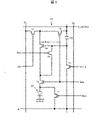
- FIG. 2 is a circuit diagram showing a pixel circuit of this embodiment.
- the pixel circuit PC the pixel capacitance Cp, the transistor T1 in which the gate electrode is connected to the scanning signal line GYn-2 in the previous stage (n-2 stages), and the scanning signal line in which the gate electrode is in its own stage (n stages).
- T2 setting transistor
- transistor T3 writing transistor
- transistor T4 transistor T4 that controls the current value of the light emitting element ED.
- the drive transistor the transistor T5 in which the gate electrode is connected to the light emission control signal line EMn of its own stage (n stage), the transistor T6 in which the gate electrode is connected to the light emission control signal line EMn, and the gate electrode is the light emission control signal. It includes an initialization transistor T7 connected to the line EMn.
- the gate electrode GE of the transistor T4 is connected to the power supply line PL via the pixel capacitance Cp and is connected to the initialization signal line IL via the transistor T1.
- a high voltage side power supply (EL VDD) is supplied to the power supply line PL, and a low voltage side power supply (ELVSS) is supplied to the cathode (upper electrode 25) of the initialization signal line IL and the light emitting element ED, for example.
- the source electrode of the transistor T4 is connected to the data signal line DLj via the transistor T3 and is connected to the power supply line PL via the transistor T5.
- the drain electrode of the transistor T4 is connected to the anode (lower electrode 22) of the light emitting element ED via the transistor T6, and is also connected to the gate electrode GE of the transistor T4 via the transistor T2.
- the anode of the light emitting device ED is connected to the initialization signal line IL via the transistor T7.
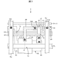
- FIG. 3 is a plan view showing the configuration of the TFT layer of the first embodiment.
- FIG. 4 is a cross-sectional view taken along the arrow of FIG.
- FIG. 5 is a timing chart showing the operation of the display device of the present embodiment.
- the TFT layer 4 includes a silicon film SFi / SHj formed on the barrier layer 3 and an inorganic insulating film 14 (first gate insulating film) covering the silicon film SFi / SFj.
- the first metal layer K1 formed above the inorganic insulating film 14 and including the scanning signal line GXn and the gate electrode GE of the transistor T4, the inorganic insulating film 16 covering the first metal layer K1, and the inorganic insulating film 16
- the second metal layer K2 formed on the upper layer and including the power supply line PL, the oxide semiconductor film ZF formed above the second metal layer K2, and the inorganic insulating film 18 (second) covering the oxide semiconductor film ZF.
- a fourth metal layer K4 formed above 20 and including a data signal line DLi / DLj and a source wiring JW, and a flattening film 21 covering the fourth metal layer K4 are provided.
- the silicon film SFi / SFj is composed of, for example, low temperature-formed polysilicon (LTPS).
- the silicon film SFi includes a conductor portion SD that functions as a conductor by being subjected to impurity doping or the like.
- the silicon film SFj includes a channel portion SC (superimposed portion with the first metal layer K1) that functions as a semiconductor, and a conductor portion SD that functions as a conductor by receiving an impurity doping or the like.
- the oxide semiconductor film ZF contains, for example, at least one element selected from indium (In), gallium (Ga), tin (Sn), hafnium (Hf), zirconium (Zr), and zinc (Zn) and oxygen. It is composed of a compound containing (for example, InGaZnO).
- the oxide semiconductor film ZF includes a channel portion (superimposed portion with the third metal layer K3) that functions as a semiconductor, and a conductor portion ZD that functions as a conductor.
- the first metal layer K1, the second metal layer K2, the third metal layer K3 and the fourth metal layer K4 include, for example, at least one of aluminum, tungsten, molybdenum, tantalum, chromium, titanium, and copper. It is composed of a layered film or a metal multi-layered film.
- the inorganic insulating film 14, 16, 18, and 20 may be composed of a single-layer film of silicon oxide (SiOx) or silicon nitride (SiNx), or may be composed of a laminated film thereof.
- the flattening film 21 can be made of a coatable organic material such as polyimide or acrylic resin.
- a signal corresponding to the video data (white gradation level in FIG. 5) is supplied to the vertical scanning period VT, and the video data is supplied to the update pause period PT.
- the data signal line DLi first data signal line
- the transistor T4 drive transistor
- the shield LE (relay electrode) that is electrically connected to the gate electrode GE of the above and the shield located between the data signal line DLi and the conductor LE in plan view and adjacent to each of the data signal line DLi and the conductor LE. Includes electrode A1.
- the conductor LE is included in the second metal layer K2, and the shield electrode is included in the first metal layer K1.
- the transistor T4 includes a channel portion SC (superimposed portion with the gate electrode GE) of the silicon film SFj, and a pixel capacitance Cp is formed between the gate electrode GE and the power supply line PL.
- the gate electrode GE is connected to the source wiring JW via the contact hole CH2, and the source wiring JW is connected to the conductor LE via the contact hole CH3. Further, the conductor portion ZD of the oxide semiconductor film ZF is provided so as to be in contact with the conductor LE.
- the first data signal line DLi and the conductor portion SD of the silicon film SFi are connected via the contact hole CH4 penetrating the inorganic insulating film 14, 16, 18, and 20, and in a plan view, the contact hole CH4 and the conductor LE.
- the shield electrode A1 is located between them.
- a signal corresponding to the video data (white gradation level in FIG. 5) is supplied to the vertical scanning period VT, and a constant potential signal not corresponding to the video data (additional voltage level in FIG. 5) is supplied to the update pause period PT.
- Data signal line DLj (second data signal line) to which Setting transistor) and included.
- the source electrode of the transistor T4 (conductor portion SD of the silicon film SFj) is connected to the second data signal line DLj via the transistor T3.
- the gate electrode GE of the transistor T4 is connected to the drain electrode of the transistor T4 (conductor portion SD of the silicon film SFj) via the transistor T2.
- the scanning signal line GXn is selected for the vertical scanning period VT and the update pause period PT (becomes active Low), and the scanning signal line GYn is selected for the vertical scanning period VT (active High). On the other hand, it is not selected for the renewal suspension period PT.
- the light emission control signal line EMn is in the active high (light-off state) during the period when at least one of the scanning signal lines GXn and GYn is selected.
- the length of the vertical scan period VT and the update pause period PT is, for example, 1/60 [second].
- the shield electrode A1 extending from the scanning signal line GXn suppresses the electric field formation (capacitive coupling) between the data signal line DLi and the conductor LE. Therefore, at the switching timing between the vertical scanning period VT and the update pause period PT (for example, the timing at which the potential of the data signal line DLi shifts from the white gradation level to the applied voltage level), the conductor LE (and the gate electrode GE) The potential is less likely to fluctuate. As a result, as shown in FIG. 5, the luminance difference between the refresh frame period RT and the non-refresh frame period NT in the sub-pixel SP is reduced. As a result, flicker (flickering of the screen) can be suppressed.
- the switching timing between the vertical scanning period VT and the update pause period PT (the timing at which the potential of the data signal line DLi shifts from the white gradation level to the applied voltage level). ) Raises the potential of the conductor LE (and the gate electrode GE). Therefore, in the sub-pixel SP, the luminance difference between the refresh frame period RT and the non-refresh frame period NT becomes large, and there is a possibility that low-frequency flicker may be visually recognized.
- the shield electrode A1 is included in the first metal layer K1, it is difficult to short-circuit both the data signal line DLi contained in the fourth metal layer K4 and the conductor LE included in the second metal layer K2.
- the constant potential signal (additional voltage level) in the update pause period PT may be a predetermined level from the white gradation level to the black gradation level.
- FIG. 5 shows a low frequency drive (refresh frequency 20 Hz) in which one update pause period PT follows one vertical scan period, which is an example and one update pause period PT after one vertical scan period. It may be a low frequency drive (refresh frequency is 30 Hz) followed by a low frequency drive (refresh frequency 10 Hz) in which one vertical scan period is followed by five update pause periods PT.
- FIG. 7 is a plan view showing the configuration of the TFT layer of the second embodiment.
- FIG. 8 is a cross-sectional view taken along the arrow of FIG. 7.
- the island-shaped electrode Q4 included in the fourth metal layer K4 and superimposing on the shield electrode A1 of the first metal layer K1 is provided, and the shield electrode A1 and the island-shaped electrode IE are provided with the inorganic insulating films 16 and 18. -Connected by a contact hole CHa penetrating 20. In this way, the electric field formation between the data signal line DLi and the conductor LE is suppressed more effectively.
- FIG. 9 is a plan view showing the configuration of the TFT layer of the third embodiment.
- FIG. 10 is a cross-sectional view taken along the arrow of FIG.
- the shield electrode A1 is extended from the scanning signal line GXn, but the present invention is not limited to this.
- From the scanning signal line GYn-2 scanning signal line controlling the transistor T1 in the own stage and the transistor T2 in the previous stage, see FIG. 2) included in the third metal layer K3 as in the third embodiment, in a plan view.
- a shield electrode A3 extending between the data signal line DLi and the conductor LE may be provided.
- the shield electrode A3 is included in the third metal layer K3, it is difficult to short-circuit both the data signal line DLi contained in the fourth metal layer K4 and the conductor LE included in the second metal layer K2.
- the gate electrode of the drive transistor is included in the first metal layer
- the first data signal line is included in the fourth metal layer
- the first data signal line and the conductor portion of the silicon film are connected via a contact hole.
- the gate electrode includes a writing transistor connected to the second scanning signal line.
- the source electrode of the drive transistor is connected to the second data signal line via the write transistor.
- the first scanning signal line is included in the first metal layer,
- the display device according to, for example, the fifth aspect, wherein the shield electrode extends from the first scanning signal line.
- a third scanning signal line included in the third metal layer is provided.
- the display device according to, for example, the fifth aspect, wherein the shield electrode extends from the third scanning signal line.
- Display device Light emitting element K1 to K4 1st to 4th metal layers SFi / SFj Silicon film SD Silicon film conductor part ZF Oxide semiconductor film ZD Oxide semiconductor film conductor part T2 setting Transistor T3 Write Transistor T4 Drive Transistor GE (Drive Transistor) Gate Electrode LE Conductor A1 Shield Electrode A3 Shield Electrode Cp Pixel Capacity DLi Data Signal Line (1st Data Signal Line) DLj data signal line (second data signal line) GXn scanning signal line (first scanning signal line) GYn scanning signal line (second scanning signal line) GYn-2 scanning signal line (third scanning signal line)
Landscapes
- Engineering & Computer Science (AREA)
- Microelectronics & Electronic Packaging (AREA)
- Physics & Mathematics (AREA)
- General Physics & Mathematics (AREA)
- Theoretical Computer Science (AREA)
- Computer Hardware Design (AREA)
- Geometry (AREA)
- Devices For Indicating Variable Information By Combining Individual Elements (AREA)
- Control Of Indicators Other Than Cathode Ray Tubes (AREA)
- Electroluminescent Light Sources (AREA)
Abstract
Description
本発明は、表示装置に関する。 The present invention relates to a display device.
特許文献1には、発光素子を用いた表示装置において、高周波数でリフレッシュ(表示データの更新)を行うモードと、低周波数でリフレッシュを行うモード(低周波数駆動)とを有する表示装置が開示されている。 Patent Document 1 discloses a display device using a light emitting element, which has a mode for refreshing at a high frequency (update of display data) and a mode for refreshing at a low frequency (low frequency drive). ing.
このような低周波数駆動では、リフレッシュを行うフレーム期間と、リフレッシュを行わないフレーム期間との間に輝度差が生じ、フリッカ(画面のちらつき)として視認される場合がある。 In such a low frequency drive, a brightness difference occurs between the frame period in which refreshing is performed and the frame period in which refreshing is not performed, which may be visually recognized as flicker (flickering of the screen).
本発明の一態様にかかる表示装置は、発光素子と、垂直走査期間に映像データに対応する信号が供給され、更新休止期間に映像データに対応しない信号が供給される第1データ信号線と、前記発光素子の電流値を制御する駆動トランジスタと、前記駆動トランジスタのゲート電極と電気的に接続する導電体と、平面視において、前記第1データ信号線および前記導電体間に位置するとともに、前記第1データ信号線および前記導電体それぞれに隣接するシールド電極とを備える。 The display device according to one aspect of the present invention includes a light emitting element, a first data signal line to which a signal corresponding to video data is supplied during a vertical scanning period, and a first data signal line to which a signal corresponding to video data is supplied during an update pause period. The drive transistor that controls the current value of the light emitting element, the conductor that is electrically connected to the gate electrode of the drive transistor, are located between the first data signal line and the conductor in a plan view, and the above. A first data signal line and a shield electrode adjacent to each of the conductors are provided.
本発明の一態様によれば、低周波数駆動を行う表示装置のフリッカを抑制することができる。 According to one aspect of the present invention, flicker of a display device that drives at a low frequency can be suppressed.
図1(a)は、本実施形態の表示装置の構成を示す模式的な平面図であり、図1(b)は、本実施形態の表示装置の構成を示す模式的な断面図である。図1に示すように、表示装置10は、発光素子EDおよびこれを制御する画素回路PCを含むサブ画素SPを複数備え、例えば、リフレッシュ周波数60Hz未満の低周波駆動を行う(後述)。画素回路PCは、データ信号線DLi・DLj、走査信号線GXn・GYn、発光制御信号線EMn等の複数の信号線に接続される。
FIG. 1A is a schematic plan view showing the configuration of the display device of the present embodiment, and FIG. 1B is a schematic cross-sectional view showing the configuration of the display device of the present embodiment. As shown in FIG. 1, the
表示装置10においては、基板2上に、バリア層3、画素回路PCを含む薄膜トランジスタ層(TFT層)4、発光素子EDを含む発光素子層5、封止層6、および機能層7がこの順に設けられる。
In the
基板2は、ガラス基板、あるいは、ポリイミド等の樹脂を主成分とする可撓性基板であり、例えば、2層のポリイミド膜およびこれらに挟まれた無機膜によって基板2を構成することもできる。バリア層3は、水、酸素等の異物の侵入を防ぐ無機絶縁層で構成することができる。TFT層4には、発光素子EDを制御する画素回路PCが形成される(後述)。
The
発光素子層5は、下部電極22と、下部電極22のエッジを覆う絶縁性のエッジカバー膜23と、エッジカバー膜23よりも上層のEL(エレクトロルミネッセンス)層24と、EL層24よりも上層の上部電極25とを含む。エッジカバー膜23は、例えば、ポリイミド、アクリル樹脂等の有機材料を塗布した後にフォトリソグラフィよってパターニングすることで形成される。
The light
発光素子層5には、発光色が異なる複数の発光素子EDが形成され、各発光素子が、島状の下部電極22、発光層を含むEL層24、および上部電極25を含む。上部電極25は、複数の発光素子EDで共通する、ベタ状の共通電極である。
A plurality of light emitting elements EDs having different light emitting colors are formed in the light
発光素子EDは、例えば、発光層として有機層を含むOLED(有機発光ダイオード)であってもよいし、発光層として量子ドット層を含むQLED(量子ドット発光ダイオード)であってもよい。 The light emitting element ED may be, for example, an OLED (organic light emitting diode) including an organic layer as a light emitting layer, or a QLED (quantum dot light emitting diode) including a quantum dot layer as a light emitting layer.
EL層24は、例えば、下層側から順に、正孔注入層、正孔輸送層、発光層、電子輸送層、電子注入層を積層することで構成される。発光層は、蒸着法あるいはインクジェット法、フォトリソグラフィ法によって、エッジカバー膜23の開口(サブ画素ごと)に、島状に形成される。他の層は、島状あるいはベタ状(共通層)に形成する。また、正孔注入層、正孔輸送層、電子輸送層、電子注入層のうち1以上の層を形成しない構成とすることもできる。
The
下部電極22(アノード)は、例えばITO(Indium Tin Oxide)とAg(銀)あるいはAgを含む合金との積層によって構成される、光反射電極である。上部電極25(カソード)は、例えばマグネシウム銀合金等の金属薄膜で構成され、光透過性を有する。 The lower electrode 22 (anode) is a light reflecting electrode composed of, for example, a laminate of ITO (Indium Tin Oxide) and an alloy containing Ag (silver) or Ag. The upper electrode 25 (cathode) is made of a metal thin film such as a magnesium-silver alloy and has light transmittance.
発光素子EDがOLEDである場合、下部電極22および上部電極25間の駆動電流によって正孔と電子が発光層内で再結合し、これによって生じたエキシトンが基底状態に遷移する過程で光が放出される。発光素子EDがQLEDである場合、下部電極22および上部電極25間の駆動電流によって正孔と電子が発光層内で再結合し、これによって生じたエキシトンが、量子ドットの伝導帯準位(conduction band)から価電子帯準位(valence band)に遷移する過程で光が放出される。
When the light emitting element ED is an OLED, holes and electrons are recombined in the light emitting layer by the driving current between the
発光素子層5を覆う封止層6は、水、酸素等の異物の発光素子層5への浸透を防ぐ層であり、例えば、2層の無機封止膜とこれら間に形成される有機膜とで構成することができる。機能層7は、光学制御、タッチセンサ、表面保護等の各種機能を有する層である。
The sealing
図2は、本実施形態の画素回路を示す回路図である。画素回路PCは、画素容量Cpと、ゲート電極が前々段(n-2段)の走査信号線GYn-2に接続されるトランジスタT1と、ゲート電極が自段(n段)の走査信号線GYnに接続されるT2(設定トランジスタ)と、ゲート電極が自段(n段)の走査信号線GXnに接続されるトランジスタT3(書き込みトランジスタ)と、発光素子EDの電流値を制御するトランジスタT4(駆動トランジスタ)と、ゲート電極が自段(n段)の発光制御信号線EMnに接続されるトランジスタT5と、ゲート電極が発光制御信号線EMnに接続されるトランジスタT6と、ゲート電極が発光制御信号線EMnに接続される初期化トランジスタT7と、を含む。 FIG. 2 is a circuit diagram showing a pixel circuit of this embodiment. In the pixel circuit PC, the pixel capacitance Cp, the transistor T1 in which the gate electrode is connected to the scanning signal line GYn-2 in the previous stage (n-2 stages), and the scanning signal line in which the gate electrode is in its own stage (n stages). T2 (setting transistor) connected to GYn, transistor T3 (writing transistor) whose gate electrode is connected to the scanning signal line GXn of its own stage (n stage), and transistor T4 (transistor T4) that controls the current value of the light emitting element ED. The drive transistor), the transistor T5 in which the gate electrode is connected to the light emission control signal line EMn of its own stage (n stage), the transistor T6 in which the gate electrode is connected to the light emission control signal line EMn, and the gate electrode is the light emission control signal. It includes an initialization transistor T7 connected to the line EMn.
トランジスタT4のゲート電極GEは、画素容量Cpを介して電源線PLに接続されるとともに、トランジスタT1を介して初期化信号線ILに接続される。電源線PLには高電圧側電源(ELVDD)が供給され、初期化信号線ILおよび発光素子EDのカソード(上部電極25)には、例えば低電圧側電源(ELVSS)が供給される。 The gate electrode GE of the transistor T4 is connected to the power supply line PL via the pixel capacitance Cp and is connected to the initialization signal line IL via the transistor T1. A high voltage side power supply (EL VDD) is supplied to the power supply line PL, and a low voltage side power supply (ELVSS) is supplied to the cathode (upper electrode 25) of the initialization signal line IL and the light emitting element ED, for example.
トランジスタT4のソース電極は、トランジスタT3を介してデータ信号線DLjに接続されるとともに、トランジスタT5を介して電源線PLに接続される。トランジスタT4のドレイン電極は、トランジスタT6を介して発光素子EDのアノード(下部電極22)に接続されるとともに、トランジスタT2を介してトランジスタT4のゲート電極GEに接続される。発光素子EDのアノードは、トランジスタT7を介して初期化信号線ILに接続される。 The source electrode of the transistor T4 is connected to the data signal line DLj via the transistor T3 and is connected to the power supply line PL via the transistor T5. The drain electrode of the transistor T4 is connected to the anode (lower electrode 22) of the light emitting element ED via the transistor T6, and is also connected to the gate electrode GE of the transistor T4 via the transistor T2. The anode of the light emitting device ED is connected to the initialization signal line IL via the transistor T7.
〔実施形態1〕
図3は、実施形態1のTFT層の構成を示す平面図である。図4は、図3の矢視断面図である。図5は、本実施形態の表示装置の動作を示すタイミングチャートである。
[Embodiment 1]
FIG. 3 is a plan view showing the configuration of the TFT layer of the first embodiment. FIG. 4 is a cross-sectional view taken along the arrow of FIG. FIG. 5 is a timing chart showing the operation of the display device of the present embodiment.
図3および図4に示すように、TFT層4は、バリア層3上に形成されるシリコン膜SFi・SHjと、シリコン膜SFi・SFjを覆う無機絶縁膜14(第1ゲート絶縁膜)と、無機絶縁膜14よりも上層に形成され、走査信号線GXnおよびトランジスタT4のゲート電極GEを含む第1金属層K1と、第1金属層K1を覆う無機絶縁膜16と、無機絶縁膜16よりも上層に形成され、電源線PLを含む第2金属層K2と、第2金属層K2よりも上層に形成される酸化物半導体膜ZFと、酸化物半導体膜ZFを覆う無機絶縁膜18(第2ゲート絶縁膜)と、無機絶縁膜18よりも上層に形成され、走査信号線GYn・GYn-2を含む第3金属層K3と、第3金属層K3を覆う無機絶縁膜20と、無機絶縁膜20よりも上層に形成され、データ信号線DLi・DLjおよびソース配線JWを含む第4金属層K4と、第4金属層K4を覆う平坦化膜21とを備える。
As shown in FIGS. 3 and 4, the
シリコン膜SFi・SFjは、例えば低温形成のポリシリコン(LTPS)で構成される。シリコン膜SFiは、不純物ドープ等を受けたことで導体として機能する導体部SDを含む。シリコン膜SFjは、半導体として機能するチャネル部SC(第1金属層K1との重畳部)と、不純物ドープ等を受けたことで導体として機能する導体部SDとを含む。 The silicon film SFi / SFj is composed of, for example, low temperature-formed polysilicon (LTPS). The silicon film SFi includes a conductor portion SD that functions as a conductor by being subjected to impurity doping or the like. The silicon film SFj includes a channel portion SC (superimposed portion with the first metal layer K1) that functions as a semiconductor, and a conductor portion SD that functions as a conductor by receiving an impurity doping or the like.
酸化物半導体膜ZFは、例えば、インジウム(In)、ガリウム(Ga)、スズ(Sn)、ハフニウム(Hf)、ジルコニウム(Zr)、亜鉛(Zn)から選ばれた少なくとも一種の元素と酸素とを含む化合物(一例としては、InGaZnO)で構成される。酸化物半導体膜ZFは、半導体として機能するチャネル部(第3金属層K3との重畳部)と、導体として機能する導体部ZDとを含む。 The oxide semiconductor film ZF contains, for example, at least one element selected from indium (In), gallium (Ga), tin (Sn), hafnium (Hf), zirconium (Zr), and zinc (Zn) and oxygen. It is composed of a compound containing (for example, InGaZnO). The oxide semiconductor film ZF includes a channel portion (superimposed portion with the third metal layer K3) that functions as a semiconductor, and a conductor portion ZD that functions as a conductor.
第1金属層K1、第2金属層K2、第3金属層K3および第4金属層K4は、例えば、アルミニウム、タングステン、モリブデン、タンタル、クロム、チタン、および銅の少なくとも1つを含む、金属単層膜あるいは金属複層膜によって構成される。 The first metal layer K1, the second metal layer K2, the third metal layer K3 and the fourth metal layer K4 include, for example, at least one of aluminum, tungsten, molybdenum, tantalum, chromium, titanium, and copper. It is composed of a layered film or a metal multi-layered film.
無機絶縁膜14・16・18・20は、酸化シリコン(SiOx)あるいは窒化シリコン(SiNx)の単層膜で構成してもよいし、これらの積層膜で構成してもよい。平坦化膜21は、例えば、ポリイミド、アクリル樹脂等の塗布可能な有機材料によって構成することができる。
The inorganic insulating
図2~図5に示すように、実施形態1のTFT層4は、垂直走査期間VTに映像データに対応する信号(図5では白階調レベル)が供給され、更新休止期間PTに映像データに対応しない定電位信号(図5では加電圧レベル)が供給されるデータ信号線DLi(第1データ信号線)と、発光素子EDの電流値を制御するトランジスタT4(駆動トランジスタ)と、トランジスタT4のゲート電極GEと電気的に接続する導電体LE(中継電極)と、平面視において、データ信号線DLiおよび導電体LE間に位置するとともに、データ信号線DLiおよび導電体LEそれぞれに隣接するシールド電極A1とを含む。導電体LEは第2金属層K2に含まれ、シールド電極は第1金属層K1に含まれる。
As shown in FIGS. 2 to 5, in the
トランジスタT4は、シリコン膜SFjのチャネル部SC(ゲート電極GEとの重畳部)を含み、ゲート電極GEおよび電源線PL間に画素容量Cpが形成される。ゲート電極GEは、コンタクトホールCH2を介してソース配線JWに接続され、ソース配線JWは、コンタクトホールCH3を介して導電体LEに接続される。また、導電体LEと接触するように、酸化物半導体膜ZFの導体部ZDが設けられる。 The transistor T4 includes a channel portion SC (superimposed portion with the gate electrode GE) of the silicon film SFj, and a pixel capacitance Cp is formed between the gate electrode GE and the power supply line PL. The gate electrode GE is connected to the source wiring JW via the contact hole CH2, and the source wiring JW is connected to the conductor LE via the contact hole CH3. Further, the conductor portion ZD of the oxide semiconductor film ZF is provided so as to be in contact with the conductor LE.
第1データ信号線DLiとシリコン膜SFiの導体部SDとが無機絶縁膜14・16・18・20を貫通するコンタクトホールCH4 を介して接続され、平面視においては、コンタクトホールCH4および導電体LE間にシールド電極A1が位置する。
The first data signal line DLi and the conductor portion SD of the silicon film SFi are connected via the contact hole CH4 penetrating the inorganic insulating
TFT層4は、垂直走査期間VTに映像データに対応する信号(図5では白階調レベル)が供給され、更新休止期間PTに映像データに対応しない定電位信号(図5では加電圧レベル)が供給されるデータ信号線DLj(第2データ信号線)と、ゲート電極が走査信号線GXnに接続されたトランジスタT3(書き込みトランジスタ)と、ゲート電極が走査信号線GYnに接続されるトランジスタT2(設定トランジスタ)とを含む。
In the
トランジスタT4のソース電極(シリコン膜SFjの導体部SD)は、トランジスタT3を介して第2データ信号線DLjに接続される。トランジスタT4のゲート電極GEは、トランジスタT2を介してトランジスタT4のドレイン電極(シリコン膜SFjの導体部SD)に接続される。 The source electrode of the transistor T4 (conductor portion SD of the silicon film SFj) is connected to the second data signal line DLj via the transistor T3. The gate electrode GE of the transistor T4 is connected to the drain electrode of the transistor T4 (conductor portion SD of the silicon film SFj) via the transistor T2.
図5に示すように、走査信号線GXnは、垂直走査期間VTおよび更新休止期間PTそれぞれにおいて選択され(アクティブLowとなり)、走査信号線GYnは、垂直走査期間VTに選択される(アクティブHighとなる)一方、更新休止期間PTには選択されない。発光制御信号線EMnについては、走査信号線GXn・GYnの少なくとも一方が選択されている期間はアクティブHigh(消灯状態)となる。垂直走査期間VTおよび更新休止期間PTの長さは、例えば、1/60〔秒〕である。 As shown in FIG. 5, the scanning signal line GXn is selected for the vertical scanning period VT and the update pause period PT (becomes active Low), and the scanning signal line GYn is selected for the vertical scanning period VT (active High). On the other hand, it is not selected for the renewal suspension period PT. The light emission control signal line EMn is in the active high (light-off state) during the period when at least one of the scanning signal lines GXn and GYn is selected. The length of the vertical scan period VT and the update pause period PT is, for example, 1/60 [second].
実施形態1では、走査信号線GXnから延伸するシールド電極A1が、データ信号線DLiおよび導電体LE間の電界形成(容量カップリング)を抑制する。このため、垂直走査期間VTと更新休止期間PTとの切り替わりタイミング(例えば、データ信号線DLiの電位が白階調レベルから加電圧レベルにシフトするタイミング)で導電体LE(およびゲート電極GE)の電位が変動しにくくなる。これにより、図5に示すように、サブ画素SPにおける、リフレッシュフレーム期間RTおよび非リフレッシュフレーム期間NT間の輝度差が低減する。これにより、フリッカ(画面のちらつき)を抑制することができる。 In the first embodiment, the shield electrode A1 extending from the scanning signal line GXn suppresses the electric field formation (capacitive coupling) between the data signal line DLi and the conductor LE. Therefore, at the switching timing between the vertical scanning period VT and the update pause period PT (for example, the timing at which the potential of the data signal line DLi shifts from the white gradation level to the applied voltage level), the conductor LE (and the gate electrode GE) The potential is less likely to fluctuate. As a result, as shown in FIG. 5, the luminance difference between the refresh frame period RT and the non-refresh frame period NT in the sub-pixel SP is reduced. As a result, flicker (flickering of the screen) can be suppressed.
図6に示すように、シールド電極A1を設けない参考例では、垂直走査期間VTと更新休止期間PTとの切り替わりタイミング(データ信号線DLiの電位が白階調レベルから加電圧レベルにシフトするタイミング)で導電体LE(およびゲート電極GE)の電位が突き上げられる。このため、サブ画素SPにおける、リフレッシュフレーム期間RTおよび非リフレッシュフレーム期間NT間の輝度差が大きくなり、低周波フリッカが視認されるおそれがある。 As shown in FIG. 6, in the reference example in which the shield electrode A1 is not provided, the switching timing between the vertical scanning period VT and the update pause period PT (the timing at which the potential of the data signal line DLi shifts from the white gradation level to the applied voltage level). ) Raises the potential of the conductor LE (and the gate electrode GE). Therefore, in the sub-pixel SP, the luminance difference between the refresh frame period RT and the non-refresh frame period NT becomes large, and there is a possibility that low-frequency flicker may be visually recognized.
実施形態1では、シールド電極A1が第1金属層K1に含まれるため、第4金属層K4に含まれるデータ信号線DLiとも、第2金属層K2に含まれる導電体LEとも短絡しにくい。 In the first embodiment, since the shield electrode A1 is included in the first metal layer K1, it is difficult to short-circuit both the data signal line DLi contained in the fourth metal layer K4 and the conductor LE included in the second metal layer K2.
また、更新休止期間PTにおいても走査信号線GXnを選択(トランジスタT3をON)し、トランジスタT4のソース電極にバイアス(加電圧レベル)をかけているため、リフレッシュフレーム期間RTおよび非リフレッシュフレーム期間NT間の輝度差がさらに抑えられる。なお、更新休止期間PTにおける定電位信号(加電圧レベル)については、白階調レベルから黒階調レベルまでの所定のレベルとすればよい。 Further, since the scanning signal line GXn is selected (transistor T3 is turned on) and the source electrode of the transistor T4 is biased (added voltage level) even in the update pause period PT, the refresh frame period RT and the non-refresh frame period NT The difference in brightness between them is further suppressed. The constant potential signal (additional voltage level) in the update pause period PT may be a predetermined level from the white gradation level to the black gradation level.
図5では、1つの垂直走査期間後に1つの更新休止期間PTが続く低周波駆動(リフレッシュ周波数20Hz)を示しているが、これは一例であり、1つの垂直走査期間後に1つの更新休止期間PTが続く低周波駆動(リフレッシュ周波数が30Hz)であってもよいし、1つの垂直走査期間後に5つの更新休止期間PTが続く低周波駆動(リフレッシュ周波数10Hz)であってもよい。
FIG. 5 shows a low frequency drive (refresh
〔実施形態2〕
図7は、実施形態2のTFT層の構成を示す平面図である。図8は、図7の矢視断面図である。実施形態2では、第4金属層K4に含まれ、第1金属層K1のシールド電極A1と重畳する島状電極Q4を設け、シールド電極A1と島状電極IEとを、無機絶縁膜16・18・20を貫通するコンタクトホールCHaによって接続する。こうすれば、データ信号線DLiおよび導電体LE間の電界形成がより効果的に抑制される。
[Embodiment 2]
FIG. 7 is a plan view showing the configuration of the TFT layer of the second embodiment. FIG. 8 is a cross-sectional view taken along the arrow of FIG. 7. In the second embodiment, the island-shaped electrode Q4 included in the fourth metal layer K4 and superimposing on the shield electrode A1 of the first metal layer K1 is provided, and the shield electrode A1 and the island-shaped electrode IE are provided with the inorganic insulating
〔実施形態3〕
図9は、実施形態3のTFT層の構成を示す平面図である。図10は、図9の矢視断面図である。実施形態1・2では、シールド電極A1を走査信号線GXnから延伸させているがこれに限定されない。実施形態3のように、第3金属層K3に含まれる走査信号線GYn-2(自段のトランジスタT1および前々段のトランジスタT2を制御する走査信号線、図2参照)から、平面視においてデータ信号線DLiおよび導電体LE間に延伸するシールド電極A3を設けてもよい。
[Embodiment 3]
FIG. 9 is a plan view showing the configuration of the TFT layer of the third embodiment. FIG. 10 is a cross-sectional view taken along the arrow of FIG. In the first and second embodiments, the shield electrode A1 is extended from the scanning signal line GXn, but the present invention is not limited to this. From the scanning signal line GYn-2 (scanning signal line controlling the transistor T1 in the own stage and the transistor T2 in the previous stage, see FIG. 2) included in the third metal layer K3 as in the third embodiment, in a plan view. A shield electrode A3 extending between the data signal line DLi and the conductor LE may be provided.
実施形態3では、シールド電極A3が第3金属層K3に含まれるため、第4金属層K4に含まれるデータ信号線DLiとも、第2金属層K2に含まれる導電体LEとも短絡しにくい。 In the third embodiment, since the shield electrode A3 is included in the third metal layer K3, it is difficult to short-circuit both the data signal line DLi contained in the fourth metal layer K4 and the conductor LE included in the second metal layer K2.
上述の各実施形態は、例示および説明を目的とするものであり、限定を目的とするものではない。これら例示および説明に基づけば、多くの変形形態が可能になることが、当業者には明らかである。 Each of the above embodiments is for the purpose of illustration and explanation, not for the purpose of limitation. Based on these examples and explanations, it will be apparent to those skilled in the art that many variants are possible.
〔まとめ〕
〔態様1〕
発光素子と、
垂直走査期間に映像データに対応する信号が供給され、更新休止期間に映像データに対応しない信号が供給される第1データ信号線と、
前記発光素子の電流値を制御する駆動トランジスタと、
前記駆動トランジスタのゲート電極と電気的に接続する導電体と、
平面視において、前記第1データ信号線および前記導電体間に位置するとともに、前記第1データ信号線および前記導電体それぞれに隣接するシールド電極と、を備える表示装置。
〔summary〕
[Aspect 1]
With a light emitting element
The first data signal line to which the signal corresponding to the video data is supplied during the vertical scanning period and the signal not corresponding to the video data is supplied during the update pause period.
A drive transistor that controls the current value of the light emitting element,
A conductor electrically connected to the gate electrode of the drive transistor and
A display device that is located between the first data signal line and the conductor in a plan view and includes a shield electrode adjacent to each of the first data signal line and the conductor.
〔態様2〕
前記シールド電極は、前記第1データ信号線および前記導電体間の電界形成を抑制する、例えば態様1に記載の表示装置。
[Aspect 2]
The display device according to, for example, embodiment 1, wherein the shield electrode suppresses electric field formation between the first data signal line and the conductor.
〔態様3〕
シリコン膜と、前記シリコン膜よりも上層の第1金属層と、前記第1金属層よりも上層の第2金属層と、前記第2金属層よりも上層の酸化物半導体膜と、前記酸化物半導体膜よりも上層の第3金属層と、前記第3金属層よりも上層の第4金属層とを含む、例えば態様1または2に記載の表示装置。
[Aspect 3]
A silicon film, a first metal layer above the silicon film, a second metal layer above the first metal layer, an oxide semiconductor film above the second metal layer, and the oxide. The display device according to, for example,
〔態様4〕
前記駆動トランジスタのゲート電極が第1金属層に含まれ、
前記第1データ信号線が第4金属層に含まれ、
前記導電体が第2金属層に含まれる、例えば態様3に記載の表示装置。
[Aspect 4]
The gate electrode of the drive transistor is included in the first metal layer,
The first data signal line is included in the fourth metal layer,
The display device according to, for example, the third aspect, wherein the conductor is included in the second metal layer.
〔態様5〕
前記シールド電極が、前記第1金属層または前記第3金属層に含まれる、例えば態様4に記載の表示装置。
[Aspect 5]
The display device according to, for example, the fourth aspect, wherein the shield electrode is included in the first metal layer or the third metal layer.
〔態様6〕
前記第1データ信号線と前記シリコン膜の導体部とがコンタクトホールを介して接続され、
平面視において、前記シールド電極が、前記コンタクトホールおよび前記導電体間に位置する、例えば態様4に記載の表示装置。
[Aspect 6]
The first data signal line and the conductor portion of the silicon film are connected via a contact hole.
The display device according to, for example,
〔態様7〕
前記酸化物半導体膜の導体部が前記導電体と接触するように設けられている、例えば態様4に記載の表示装置。
[Aspect 7]
The display device according to, for example, the fourth aspect, wherein the conductor portion of the oxide semiconductor film is provided so as to be in contact with the conductor.
〔態様8〕
前記映像データに対応しない信号が定電位信号である、例えば態様1に記載の表示装置。
[Aspect 8]
The display device according to, for example, the first aspect, wherein the signal that does not correspond to the video data is a constant potential signal.
〔態様9〕
第1走査信号線と、
垂直走査期間に映像データに対応する信号が供給され、更新休止期間に映像データに対応しない信号が供給される第2データ信号線と、
ゲート電極が前記第2走査信号線に接続された書き込みトランジスタとを備え、
前記駆動トランジスタのソース電極は、前記書き込みトランジスタを介して前記第2データ信号線に接続され、
前記第1走査信号線は、前記垂直走査期間および前記更新休止期間それぞれにおいて選択される、例えば態様5に記載の表示装置。
[Aspect 9]
The first scan signal line and
A second data signal line to which a signal corresponding to the video data is supplied during the vertical scanning period and a signal not corresponding to the video data is supplied during the update pause period.
The gate electrode includes a writing transistor connected to the second scanning signal line.
The source electrode of the drive transistor is connected to the second data signal line via the write transistor.
The display device according to, for example, the fifth aspect, wherein the first scanning signal line is selected in each of the vertical scanning period and the update pause period.
〔態様10〕
前記第1走査信号線が前記第1金属層に含まれ、
前記シールド電極は、前記第1走査信号線から延伸する、例えば態様5に記載の表示装置。
[Aspect 10]
The first scanning signal line is included in the first metal layer,
The display device according to, for example, the fifth aspect, wherein the shield electrode extends from the first scanning signal line.
〔態様11〕
前記第4金属層に形成され、前記シールド電極と重畳する島状電極を備え、
前記シールド電極と前記島状電極とがコンタクトホールを介して接続されている、例えば態様10に記載の表示装置。
[Aspect 11]
It is provided with an island-shaped electrode formed on the fourth metal layer and superposed on the shield electrode.
The display device according to, for example,
〔態様12〕
第2走査信号線と、
ゲート電極が前記第2走査信号線に接続される設定トランジスタとを備え、
前記駆動トランジスタのゲート電極は、前記設定トランジスタを介して前記駆動トランジスタのドレイン電極に接続され、
前記第2走査信号線は、前記垂直走査期間に選択されるが、前記更新休止期間には選択されない、例えば態様10に記載の表示装置。
[Aspect 12]
The second scan signal line and
A setting transistor in which the gate electrode is connected to the second scanning signal line is provided.
The gate electrode of the drive transistor is connected to the drain electrode of the drive transistor via the setting transistor.
The display device according to, for example,
〔態様13〕
前記第3金属層に含まれる第3走査信号線を備え、
前記シールド電極は、前記第3走査信号線から延伸する、例えば態様5に記載の表示装置。
[Aspect 13]
A third scanning signal line included in the third metal layer is provided.
The display device according to, for example, the fifth aspect, wherein the shield electrode extends from the third scanning signal line.
2 基板
3 バリア層
4 薄膜トランジスタ層(TFT層)
5 発光素子層
6 封止層
10 表示装置
ED 発光素子
K1~K4 第1~第4金属層
SFi・SFj シリコン膜
SD シリコン膜の導体部
ZF 酸化物半導体膜
ZD 酸化物半導体膜の導体部
T2 設定トランジスタ
T3 書き込みトランジスタ
T4 駆動トランジスタ
GE (駆動トランジスタの)ゲート電極
LE 導電体
A1 シールド電極
A3 シールド電極
Cp 画素容量
DLi データ信号線(第1データ信号線)
DLj データ信号線(第2データ信号線)
GXn 走査信号線(第1走査信号線)
GYn 走査信号線(第2走査信号線)
GYn-2 走査信号線(第3走査信号線)
2
5 Light emitting
DLj data signal line (second data signal line)
GXn scanning signal line (first scanning signal line)
GYn scanning signal line (second scanning signal line)
GYn-2 scanning signal line (third scanning signal line)
Claims (13)
垂直走査期間に映像データに対応する信号が供給され、更新休止期間に映像データに対応しない信号が供給される第1データ信号線と、
前記発光素子の電流値を制御する駆動トランジスタと、
前記駆動トランジスタのゲート電極と電気的に接続する導電体と、
平面視において、前記第1データ信号線および前記導電体間に位置するとともに、前記第1データ信号線および前記導電体それぞれに隣接するシールド電極と、を備える表示装置。 With a light emitting element
The first data signal line to which the signal corresponding to the video data is supplied during the vertical scanning period and the signal not corresponding to the video data is supplied during the update pause period.
A drive transistor that controls the current value of the light emitting element,
A conductor electrically connected to the gate electrode of the drive transistor and
A display device that is located between the first data signal line and the conductor in a plan view and includes a shield electrode adjacent to each of the first data signal line and the conductor.
前記第1データ信号線が第4金属層に含まれ、
前記導電体が第2金属層に含まれる請求項3に記載の表示装置。 The gate electrode of the drive transistor is included in the first metal layer,
The first data signal line is included in the fourth metal layer,
The display device according to claim 3, wherein the conductor is included in the second metal layer.
平面視において、前記シールド電極が、前記コンタクトホールおよび前記導電体間に位置する請求項4に記載の表示装置。 The first data signal line and the conductor portion of the silicon film are connected via a contact hole.
The display device according to claim 4, wherein the shield electrode is located between the contact hole and the conductor in a plan view.
垂直走査期間に映像データに対応する信号が供給され、更新休止期間に映像データに対応しない信号が供給される第2データ信号線と、
ゲート電極が前記第1走査信号線に接続された書き込みトランジスタとを備え、
前記駆動トランジスタのソース電極は、前記書き込みトランジスタを介して前記第2データ信号線に接続され、
前記第1走査信号線は、前記垂直走査期間および前記更新休止期間それぞれにおいて選択される請求項5に記載の表示装置。 The first scan signal line and
A second data signal line to which a signal corresponding to the video data is supplied during the vertical scanning period and a signal not corresponding to the video data is supplied during the update pause period.
The gate electrode includes a writing transistor connected to the first scanning signal line.
The source electrode of the drive transistor is connected to the second data signal line via the write transistor.
The display device according to claim 5, wherein the first scanning signal line is selected in each of the vertical scanning period and the update pause period.
前記シールド電極は、前記第1走査信号線から延伸する請求項9に記載の表示装置。 The first scanning signal line is included in the first metal layer,
The display device according to claim 9, wherein the shield electrode extends from the first scanning signal line.
前記シールド電極と前記島状電極とがコンタクトホールを介して接続されている請求項10に記載の表示装置。 It is provided with an island-shaped electrode formed on the fourth metal layer and superposed on the shield electrode.
The display device according to claim 10, wherein the shield electrode and the island-shaped electrode are connected via a contact hole.
ゲート電極が前記第2走査信号線に接続される設定トランジスタとを備え、
前記駆動トランジスタのゲート電極は、前記設定トランジスタを介して前記駆動トランジスタのドレイン電極に接続され、
前記第2走査信号線は、前記垂直走査期間に選択されるが、前記更新休止期間には選択されない請求項10に記載の表示装置。 The second scan signal line and
A setting transistor in which the gate electrode is connected to the second scanning signal line is provided.
The gate electrode of the drive transistor is connected to the drain electrode of the drive transistor via the setting transistor.
The display device according to claim 10, wherein the second scanning signal line is selected during the vertical scanning period but not during the update pause period.
前記シールド電極は、前記第3走査信号線から延伸する請求項5に記載の表示装置。 A third scanning signal line included in the third metal layer is provided.
The display device according to claim 5, wherein the shield electrode extends from the third scanning signal line.
Priority Applications (2)
| Application Number | Priority Date | Filing Date | Title |
|---|---|---|---|
| PCT/JP2020/046314 WO2022123776A1 (en) | 2020-12-11 | 2020-12-11 | Display device |
| US18/266,275 US12082455B2 (en) | 2020-12-11 | 2020-12-11 | Display device |
Applications Claiming Priority (1)
| Application Number | Priority Date | Filing Date | Title |
|---|---|---|---|
| PCT/JP2020/046314 WO2022123776A1 (en) | 2020-12-11 | 2020-12-11 | Display device |
Publications (1)
| Publication Number | Publication Date |
|---|---|
| WO2022123776A1 true WO2022123776A1 (en) | 2022-06-16 |
Family
ID=81974280
Family Applications (1)
| Application Number | Title | Priority Date | Filing Date |
|---|---|---|---|
| PCT/JP2020/046314 Ceased WO2022123776A1 (en) | 2020-12-11 | 2020-12-11 | Display device |
Country Status (2)
| Country | Link |
|---|---|
| US (1) | US12082455B2 (en) |
| WO (1) | WO2022123776A1 (en) |
Cited By (1)
| Publication number | Priority date | Publication date | Assignee | Title |
|---|---|---|---|---|
| WO2024000701A1 (en) * | 2022-06-29 | 2024-01-04 | 武汉华星光电半导体显示技术有限公司 | Pixel circuit and display panel |
Citations (7)
| Publication number | Priority date | Publication date | Assignee | Title |
|---|---|---|---|---|
| JP2003271076A (en) * | 2002-03-19 | 2003-09-25 | Toshiba Corp | Display device |
| JP2009168898A (en) * | 2008-01-11 | 2009-07-30 | Sony Corp | Self-luminous display device |
| WO2011048838A1 (en) * | 2009-10-20 | 2011-04-28 | シャープ株式会社 | Active matrix substrate and organic el display device |
| JP2011146620A (en) * | 2010-01-18 | 2011-07-28 | Seiko Epson Corp | Display device and electronic apparatus |
| JP2013238724A (en) * | 2012-05-15 | 2013-11-28 | Seiko Epson Corp | Electro-optic device and electronic apparatus |
| JP2018136565A (en) * | 2018-04-11 | 2018-08-30 | セイコーエプソン株式会社 | Electrooptical device and electronic device |
| US20200027939A1 (en) * | 2018-07-17 | 2020-01-23 | Samsung Display Co., Ltd. | Pixel and organic light emitting display device including the same |
Family Cites Families (6)
| Publication number | Priority date | Publication date | Assignee | Title |
|---|---|---|---|---|
| JP4027614B2 (en) * | 2001-03-28 | 2007-12-26 | 株式会社日立製作所 | Display device |
| CN105022540B (en) * | 2011-09-07 | 2018-11-09 | 辛纳普蒂克斯公司 | Capacitive sensing during non-display renewal time |
| KR102318265B1 (en) * | 2014-11-14 | 2021-10-27 | 삼성디스플레이 주식회사 | Organic light emitting diode display |
| KR102271115B1 (en) * | 2015-02-13 | 2021-06-30 | 삼성디스플레이 주식회사 | Organic light emitting diode display |
| JP2017015996A (en) * | 2015-07-02 | 2017-01-19 | 株式会社ジャパンディスプレイ | Display |
| JP6854625B2 (en) | 2016-11-04 | 2021-04-07 | 株式会社ジャパンディスプレイ | Display device |
-
2020
- 2020-12-11 WO PCT/JP2020/046314 patent/WO2022123776A1/en not_active Ceased
- 2020-12-11 US US18/266,275 patent/US12082455B2/en active Active
Patent Citations (7)
| Publication number | Priority date | Publication date | Assignee | Title |
|---|---|---|---|---|
| JP2003271076A (en) * | 2002-03-19 | 2003-09-25 | Toshiba Corp | Display device |
| JP2009168898A (en) * | 2008-01-11 | 2009-07-30 | Sony Corp | Self-luminous display device |
| WO2011048838A1 (en) * | 2009-10-20 | 2011-04-28 | シャープ株式会社 | Active matrix substrate and organic el display device |
| JP2011146620A (en) * | 2010-01-18 | 2011-07-28 | Seiko Epson Corp | Display device and electronic apparatus |
| JP2013238724A (en) * | 2012-05-15 | 2013-11-28 | Seiko Epson Corp | Electro-optic device and electronic apparatus |
| JP2018136565A (en) * | 2018-04-11 | 2018-08-30 | セイコーエプソン株式会社 | Electrooptical device and electronic device |
| US20200027939A1 (en) * | 2018-07-17 | 2020-01-23 | Samsung Display Co., Ltd. | Pixel and organic light emitting display device including the same |
Cited By (2)
| Publication number | Priority date | Publication date | Assignee | Title |
|---|---|---|---|---|
| WO2024000701A1 (en) * | 2022-06-29 | 2024-01-04 | 武汉华星光电半导体显示技术有限公司 | Pixel circuit and display panel |
| US12451063B2 (en) | 2022-06-29 | 2025-10-21 | Wuhan China Star Optoelectronics Semiconductor Display Technology Co. Ltd. | Pixel circuit and display panel |
Also Published As
| Publication number | Publication date |
|---|---|
| US20240049527A1 (en) | 2024-02-08 |
| US12082455B2 (en) | 2024-09-03 |
Similar Documents
| Publication | Publication Date | Title |
|---|---|---|
| US20240021162A1 (en) | Organic light-emitting diode (oled) display and method of manufacturing the same | |
| KR102769670B1 (en) | Organic light emitting diode display device | |
| US10950678B2 (en) | Thin film transistor substrate and organic light-emitting display using the same | |
| KR102268493B1 (en) | Organic light emitting diode device and method of fabricating the same | |
| US12022710B2 (en) | Organic light emitting display device | |
| JP6397654B2 (en) | Organic EL light emitting device | |
| KR102607376B1 (en) | Organic light emitting diode display device | |
| KR102789409B1 (en) | Organic light emitting diode display device | |
| JP2020109452A (en) | Display device and manufacturing method for display device | |
| WO2018225183A1 (en) | Display device, method for manufacturing display device, and apparatus for manufacturing display device | |
| JP7482299B2 (en) | Display device | |
| WO2019187159A1 (en) | Display device | |
| WO2019187074A1 (en) | Display device | |
| KR20190068878A (en) | Electroluminescent display device | |
| JP2021108366A (en) | Thin film device | |
| JP2019003040A (en) | Display | |
| US20210027718A1 (en) | Display device | |
| JP2015176800A (en) | Luminescent display device | |
| WO2021053792A1 (en) | Display device | |
| WO2022123776A1 (en) | Display device | |
| WO2019171878A1 (en) | Organic el display device | |
| JP5212683B2 (en) | Transistor panel and manufacturing method thereof | |
| US20220199955A1 (en) | Display device and manufactring method thereof | |
| WO2019138495A1 (en) | Display device | |
| US12200985B2 (en) | Display device in which the occurrence of shading is reduced without excessively increasing the pixel spacing |
Legal Events
| Date | Code | Title | Description |
|---|---|---|---|
| 121 | Ep: the epo has been informed by wipo that ep was designated in this application |
Ref document number: 20965158 Country of ref document: EP Kind code of ref document: A1 |
|
| WWE | Wipo information: entry into national phase |
Ref document number: 18266275 Country of ref document: US |
|
| NENP | Non-entry into the national phase |
Ref country code: DE |
|
| 122 | Ep: pct application non-entry in european phase |
Ref document number: 20965158 Country of ref document: EP Kind code of ref document: A1 |
|
| NENP | Non-entry into the national phase |
Ref country code: JP |