WO2022158267A1 - コンデンサ - Google Patents
コンデンサ Download PDFInfo
- Publication number
- WO2022158267A1 WO2022158267A1 PCT/JP2021/048515 JP2021048515W WO2022158267A1 WO 2022158267 A1 WO2022158267 A1 WO 2022158267A1 JP 2021048515 W JP2021048515 W JP 2021048515W WO 2022158267 A1 WO2022158267 A1 WO 2022158267A1
- Authority
- WO
- WIPO (PCT)
- Prior art keywords
- capacitor
- bus bar
- capacitor element
- heat transfer
- portions
- Prior art date
- Legal status (The legal status is an assumption and is not a legal conclusion. Google has not performed a legal analysis and makes no representation as to the accuracy of the status listed.)
- Ceased
Links
Images


Classifications
-
- H—ELECTRICITY
- H01—ELECTRIC ELEMENTS
- H01G—CAPACITORS; CAPACITORS, RECTIFIERS, DETECTORS, SWITCHING DEVICES, LIGHT-SENSITIVE OR TEMPERATURE-SENSITIVE DEVICES OF THE ELECTROLYTIC TYPE
- H01G2/00—Details of capacitors not covered by a single one of groups H01G4/00-H01G11/00
- H01G2/08—Cooling arrangements; Heating arrangements; Ventilating arrangements
-
- H—ELECTRICITY
- H01—ELECTRIC ELEMENTS
- H01G—CAPACITORS; CAPACITORS, RECTIFIERS, DETECTORS, SWITCHING DEVICES, LIGHT-SENSITIVE OR TEMPERATURE-SENSITIVE DEVICES OF THE ELECTROLYTIC TYPE
- H01G4/00—Fixed capacitors; Processes of their manufacture
- H01G4/32—Wound capacitors
Definitions
- the present invention relates to capacitors.
- the capacitor element generates heat when the capacitor is energized. In the capacitor configured as described above, heat is less likely to be released from the capacitor element because the capacitor element is embedded in the filling resin.
- the capacitor having the above configuration can be mounted in an inverter device for driving an electric motor.
- the capacitor element since a large amount of current tends to flow from the power supply device to the inverter device, a large amount of current tends to flow to the capacitor element, and heat generation of the capacitor element tends to increase.
- an object of the present invention is to provide a capacitor capable of enhancing heat dissipation from a capacitor element.
- a main aspect of the present invention relates to a capacitor.
- the capacitor according to this aspect includes a capacitor element, a first bus bar and a second bus bar respectively connected to electrodes provided on both end surfaces of the capacitor element, the entire capacitor element and the first bus bar and the second bus bar.
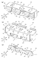
- FIG. 1(a) is a perspective view of a film capacitor according to an embodiment
- FIG. 1(b) is a side cross-sectional view of the film capacitor omitting a filling resin according to an embodiment
- FIGS. 2(a) and 2(b) are perspective views of the capacitor element unit viewed from the upper front and the upper rear, respectively, according to the embodiment.
- FIG. 3(a) is a perspective view of the capacitor element unit viewed from the front and lower side according to the embodiment, and FIG. FIG. 3 is a perspective view of the capacitor element unit viewed from below;
- FIGS. 4(a) and 4(b) are perspective views of the first bus bar viewed from above the front and the upper rear, respectively, according to the embodiment, and FIG. FIG.
- FIG. 4 is a perspective view of a second busbar as seen from above;
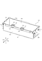
- FIG. 5 is a perspective view of a case according to the embodiment.
- FIG. 6(a) is a perspective view of a capacitor element unit viewed from the front and lower side according to a modification, and
- FIG. 6(b) is a side cross-sectional view of a film capacitor in which a filling resin is omitted according to the modification. is.
- a film capacitor 1 which is one embodiment of the capacitor of the present invention, will be described below with reference to the drawings.
- front-rear, left-right, and up-down directions are indicated in each figure as appropriate. It should be noted that the illustrated directions only indicate relative directions of the film capacitor 1, and do not indicate absolute directions. Also, for convenience of explanation, some configurations such as “bottom portion” and “front side portion” may be named according to the direction of illustration.
- FIG. 1(a) is a perspective view of the film capacitor 1
- FIG. 1(b) is a side sectional view of the film capacitor 1 with the filling resin 600 omitted.
- the film capacitor 1 includes three capacitor elements 100, a first bus bar 200, a second bus bar 300, a heat transfer member 400, a case 500, a filling resin 600.
- Three capacitor elements 100 , first bus bar 200 and second bus bar 300 are integrally assembled, and heat transfer member 400 is connected to first bus bar 200 and second bus bar 300 to form capacitor element unit 10 .
- Capacitor element unit 10 is housed in case 500, and case 500 is filled with filling resin 600, which is a coating resin.
- Filling resin 600 is a thermosetting resin, such as an epoxy resin.
- the entirety of the three capacitor elements 100 and the heat transfer member 400 and part of the first busbar 200 and the second busbar 300 are covered with the filling resin 600 inside the case 500 to be protected from moisture and impact.
- FIGS. 2(a) and 2(b) are perspective views of the capacitor element unit 10 viewed from the front upper side and the rear upper side, respectively.
- FIG. 3(a) is a perspective view of the capacitor element unit 10 viewed from the lower front
- FIG. 3(b) is a perspective view of the capacitor element unit 10 viewed from the lower front with the heat transfer member 400 removed. It is a diagram.
- FIGS. 4A and 4B are perspective views of first busbar 200 viewed from above the front and rear, respectively
- FIG. 4C is a perspective view of second busbar 300 viewed from above and from the front. It is a diagram.
- the three capacitor elements 100 are formed by stacking two aluminum-deposited metallized films on a dielectric film, winding or laminating the stacked metallized films, and pressing them into a flat shape.
- Capacitor element 100 has a shape similar to a flattened cylinder.
- a first electrode 110 is formed on one end surface 101 of the capacitor element 100 by spraying a metal such as zinc, and a second electrode 120 is formed on the other end surface 102 by similarly spraying a metal such as zinc. be.
- capacitor element 100 of the present embodiment is formed of a metallized film in which aluminum is vapor-deposited on a dielectric film. It may be formed by a film. Alternatively, capacitor element 100 may be formed of a metallized film obtained by vapor-depositing a plurality of these metals, or may be formed of a metallized film obtained by vapor-depositing an alloy of these metals. .
- the three capacitor elements 100 have one end face 101, that is, the first electrode 110, facing backward, and the other end face 102, that is, the second electrode 120, facing forward. are arranged in a row in the left-right direction so that they are adjacent to each other. First electrode 110 and second electrode 120 of three capacitor elements 100 are electrically connected to first bus bar 200 and second bus bar 300, respectively.
- the first bus bar 200 is formed by appropriately cutting out and bending a conductive material such as a copper plate. , three first extensions 250 and two second extensions 260 are integrated. In the present embodiment, first bus bar 200 is an N-pole bus bar.
- the electrode terminal portion 210 has a rectangular plate shape with two lower portions notched in a predetermined shape, and contacts the first electrodes 110 of the three capacitor elements 100 so as to cover the first electrodes 110 from behind. .
- the upper end portion of the electrode terminal portion 210 protrudes upward from the three first electrodes 110 .
- a total of nine connection pins 211 are formed in the left and right ends and two cutout portions of the electrode terminal portion 210 .
- Three connection pins 211 corresponding to each first electrode 110 are joined by a joining method such as soldering.
- two communication holes 212 are formed in the electrode terminal portion 210 at the upper end portion (the portion protruding from the first electrode 110).
- the intermediate portion 220 extends forward from the upper end (one end) of the electrode terminal portion 210 and connects to the three first connection terminal portions 230 and the second connection terminal portions 240 .
- the intermediate portion 220 is formed at three locations: a rectangular plate-shaped first portion 221 having a width wider than that of the electrode terminal portion 210 in the left-right direction, and a front end of the first portion 221, and is bent into an inverted U shape. It includes a second portion 222 and a third portion 223 rising from between the central and right second portions 222 at the front end of the first portion 221 .
- the upper surface 221a of the first portion 221 (the surface not facing the capacitor element 100) is a flat surface.
- the first portion 221 and the upper surface 221a function as a mounting portion and a mounting surface, respectively, on which the heat absorbing member 2 (described later) is mounted.
- the upper surface 221a of the first portion 221 will be referred to as a mounting surface 221a.
- the intermediate portion 220 that is, the first portion 221 is arranged along the upper portion of the peripheral surface 103 of the three capacitor elements 100 and covers the entire three capacitor elements 100 from above.
- a predetermined gap is provided between the first portion 221 and the peripheral surfaces 103 of the three capacitor elements 100 .
- the first portion 221 is provided with three (plurality of) openings 224 arranged in the left-right direction. Further, the first portion 221 is provided with protrusions 225 that protrude downward from the front edges of the respective openings 224 . The tip of projecting portion 225 contacts peripheral surface 103 of capacitor element 100 .
- the three first connection terminal portions 230 have a rectangular plate shape and extend forward from the tips of the three second portions 222 of the intermediate portion 220 .
- the second connection terminal portion 240 has a semi-elliptical plate shape and extends forward from the tip of the third portion 223 of the intermediate portion 220 .
- a circular attachment hole 241 is formed in the second connection terminal portion 240 .
- the three first extending portions 250 extend forward from the lower end (the end different from the one end) of the electrode terminal portion 210 so as to cover the lower portion of the peripheral surface 103 of the three capacitor elements 100 from below. Adjacent to the side part.
- the center first extension 250 has a rectangular plate shape, and the two left and right first extensions 250 have a U-shaped plate shape.
- the three first extending portions 250 extend from the first electrode 110 side of the peripheral surface 103 of the three capacitor elements 100 to more than a half position.
- the two second extending portions 260 extend downward from the left and right ends (one ends) of the first portion 221 of the intermediate portion 220, and extend the left and right portions of the peripheral surface 103 of the left and right ends of the capacitor element 100 to the left. These left and right portions are adjacent to cover from the left and right sides.
- the two second extensions 260 have a rectangular plate shape.
- the two second extending portions 260 extend from the upper end side of the peripheral surface 103 of the left and right ends of the capacitor element 100 to more than a half position.
- a distance equal to or greater than the spatial distance (insulation distance) required for insulation is provided. This ensures insulation between the first bus bar 200 and the second electrode 120 .
- each first extension 250 and each second extension 260 are in contact with peripheral surface 103 of capacitor element 100 .
- each first extending portion 250 and each second extending portion 260 may have a slight gap from peripheral surface 103 of capacitor element 100 .
- the second bus bar 300 is formed by appropriately cutting out and bending a conductive material such as a copper plate. It has a configuration in which and are integrated. In the present embodiment, second bus bar 300 is a P-pole bus bar.
- the electrode terminal portion 310 has a rectangular plate shape and contacts the second electrodes 120 of the three capacitor elements 100 so as to cover the second electrodes 120 from the front.
- a total of nine connection pins 311 are formed at the lower end of the electrode terminal portion 310 .
- Three connection pins 311 corresponding to each second electrode 120 are joined by a joining method such as soldering.
- the intermediate portion 320 extends obliquely forward and upward from the upper end of the electrode terminal portion 310 and connects to three first connection terminal portions 330 and second connection terminal portions 340 .
- the intermediate portion 320 is formed at three locations: a rectangular plate-shaped first portion 321 having the same width as the electrode terminal portion 310 in the left-right direction, and a front end of the first portion 321, and is bent into an inverted U shape. It includes a second portion 322 and a third portion 323 rising from between the central and left second portions 322 at the front end of the first portion 321 .
- the three first connection terminal portions 330 have a rectangular plate shape and extend forward from the tips of the three second portions 322 of the intermediate portion 320 .
- the second connection terminal portion 340 has a semi-elliptical plate shape and extends forward from the tip of the third portion 323 of the intermediate portion 320 .
- a circular attachment hole 341 is formed in the second connection terminal portion 340 .
- the heat transfer member 400 has a rectangular sheet shape, is bent into an L shape, and is connected to the first busbar 200 and the second busbar 300 using a heat-resistant adhesive or the like.
- One end of the heat transfer member 400 is connected to the electrode terminal portion 310 of the second bus bar 300 in a direction (vertical direction, front-rear direction) perpendicular to the direction in which the three capacitor elements 100 are arranged (horizontal direction). , along the peripheral surface 103 of the three capacitor elements 100 , and the other end is connected to the three first extensions 250 of the first bus bar 200 .
- the heat transfer member 400 has the same width as the width of the electrode terminal portion 310 and the width to the left and right ends of the three first extension portions 250 in the alignment direction (horizontal direction). Face close.
- the heat transfer member 400 is a highly thermally conductive insulating member, made of, for example, a silicon-based material, has insulating properties, and has a higher thermal conductivity than the filling resin 600 .
- the thermal conductivity of the filling resin 600 is approximately 0.4 to 0.5 W/m ⁇ K, while the thermal conductivity of the heat transfer member 400 is approximately 3.0 to 3.5 W/m ⁇ K. It is said that
- the first connection terminal portions 330 of the second busbar 300 are arranged next to the first connection terminal portions 230 of the first busbar 200 .
- the second connection terminal portion 240 of the first bus bar 200 is positioned between the pair of first connection terminal portions 230, 330 on the right end and the pair of first connection terminal portions 230, 330 on the center.
- the second connection terminal portion 340 of the second bus bar 300 is positioned between the first connection terminal portions 230 and 330 of the second bus bar 300 and the pair of first connection terminal portions 230 and 330 in the center.
- An insulating sheet 700 is sandwiched between the three second portions 222 of the first busbar 200 and the three second portions 322 of the second busbar 300 . Insulating sheet 700 extends below the front side of first portion 221 of intermediate portion 220 of first bus bar 200 .
- the insulating sheet 700 is made of insulating paper or an insulating resin material such as acrylic or silicon. The insulating sheet 700 ensures insulation between the first bus bar 200 and the second bus bar 300, insulation between the first bus bar 200 and the second electrodes 120 of the three capacitor elements 100, and the like.
- FIG. 5 is a perspective view of the case 500.
- FIG. 5 is a perspective view of the case 500.
- the case 500 is made of resin, for example, polyphenylene sulfide (PPS), which is a thermoplastic resin.
- PPS polyphenylene sulfide
- the case 500 is formed in a substantially rectangular parallelepiped box shape, and has a bottom portion 501, a front side portion 502, a rear side portion 503, a left side portion 504, and a right side portion 505 rising from the bottom portion 501, and has an open top surface.
- Cylindrical mounting bosses 510 are provided at the front and rear end portions of the left side portion 504 and the right side portion 505 . These mounting bosses 510 are used when the film capacitor 1 is fixed to an installation portion of an external device.
- Two terminal blocks 520 are provided at the upper end of the front side portion 502 .
- Installation surface 521 which is the upper surface of terminal block 520 , has a shape corresponding to second connection terminal portions 240 and 340 of first bus bar 200 and second bus bar 300 .
- a cylindrical nut 530 is attached to the installation surface 521 .
- the capacitor element unit 10 is accommodated in the case 500 as shown in FIG. 1(b).
- the second connection terminal portion 240 of the first busbar 200 is installed on the right terminal block 520
- the second connection terminal portion 340 of the second busbar 300 is installed on the left terminal block 520 .
- the mounting holes 241 , 341 of the second connection terminal portions 240 , 340 are fitted to the tip portion of the nut 530 .
- the three second portions 222 , 322 of the intermediate portions 220 , 320 of the first busbar 200 and the second busbar 300 straddle the upper end portion of the front side portion 502 of the case 500 .
- Most of opening 500 a of case 500 is covered with first portion 221 of intermediate portion 220 of first bus bar 200 .
- the first electrode 110 of the three capacitor elements 100 faces the inner wall surface of the rear side portion 503 of the case 500
- the second electrode 120 faces the inner wall surface of the front side portion 502 of the case 500
- the first extending portion 250 of the first bus bar 200 and the heat transfer member 400 are present between the lower portion of the peripheral surface 103 of the three capacitor elements 100 and the bottom surface portion 501 of the case 500 , and the bottom surface portion 501 close to the inner wall surface of
- the left and right second extension portions 260 of the first bus bar 200 approach the inner wall surfaces of the left side surface portion 504 and the right side surface portion 505 of the case 500, respectively.
- a filling resin 600 in a liquid state is injected into the case 500 through three openings 224 provided in the first portion 221 of the intermediate portion 220 of the first bus bar 200 .
- the three openings 224 are used to smoothly inject the filling resin 600 into the case 500. can.
- Two flow holes 212 are provided in the electrode terminal portion 210 of the first bus bar 200, and the injected filling resin 600 passes through these flow holes 212 to form the electrode terminal portion 210 and the rear side portion. 503 becomes easy to spread.
- the film capacitor 1 is completed as shown in FIG. 1(a).
- the three first connection terminal portions 230 and the second connection terminal portions 240 of the first bus bar 200 and the three first connection terminal portions 330 and the second connection terminal portions 340 of the second bus bar 300 are It is exposed from the filling resin 600 and located in the front part of the case 500 .
- the first portion 221 and the mounting surface 221 a of the intermediate portion 220 of the first bus bar 200 are exposed from the filling resin 600 .
- a constant distance is maintained between the first portion 221 of the intermediate portion 220 and the three capacitor elements 100 by the three projecting portions 225 .
- the height position of capacitor element unit 10 with respect to case 500 is determined such that first portion 221 is exposed from filling resin 600, three capacitor elements 100 are reliably buried in filling resin 600. be able to. Furthermore, in the filled resin 600 , the first bus bar 200 and the second bus bar 300 are connected via the heat transfer member 400 .
- the film capacitor 1 can be mounted, for example, in an inverter device for driving an electric motor in an electric vehicle.
- DC power is supplied to the inverter device from a power supply device (battery).
- the inverter device has an inverter circuit including an IGBT (Insulated Gate Bipolar Transistor), converts DC power into three-phase AC power, and supplies it to an electric motor.
- IGBT Insulated Gate Bipolar Transistor
- the second connection terminal portion 240 of the first bus bar 200 and the second connection terminal portion 340 of the second bus bar 300 are connected to corresponding external terminals (not shown) connected to a power supply device.
- the second connection terminal portions 240 and 340 and the external terminals are fixed to the terminal block 520 by tightening bolts (not shown) to the nuts 530 .
- External terminals (not shown) connected to inverter circuits corresponding to the three first connection terminal portions 230 of the first bus bar 200 and the three first connection terminal portions 330 of the second bus bar 300 are connected to the connector. It is connected by a connection method such as connection.
- the cooling member 2 is attached to the attachment surface 221a of the intermediate portion 220 of the first bus bar 200 (see FIG. 1(b)) in order to enhance the heat radiation effect.
- the cooling member 2 is for forcibly cooling the first bus bar 200 from the outside. be done.
- the cooling member 2 may be a cooler using a Peltier element. Insulation is provided between the cooling member 2 and the mounting surface 221a.
- the three capacitor elements 100 When the inverter device operates and the film capacitor 1 is energized, the three capacitor elements 100 generate heat. Among the three capacitor elements 100, the central capacitor element 100 is more likely to be heated to a higher temperature than the capacitor elements 100 at the left and right ends.
- first bus bar 200 The heat generated from the first electrodes 110 and the peripheral surfaces 103 of the three capacitor elements 100 is transmitted to the electrode terminal portions 210, the three first extending portions 250 and the two second extending portions 260 of the first bus bar 200. .
- cooling member 2 absorbs heat from first portion 221 of intermediate portion 220, and first portion 221 is cooled to a low temperature.
- the heat transmitted to the electrode terminal portion 210 , each first extension portion 250 and each second extension portion 260 moves to the first portion 221 of the intermediate portion 220 and travels from the first portion 221 to the cooling member 2 . released.
- first portion 221 of the intermediate portion 220 is sized to cover the three capacitor elements 100 as a whole. Therefore, the area of first bus bar 200 cooled by cooling member 2 is increased, and the amount of heat radiation to cooling member 2 can be increased.
- the heat generated from the second electrodes 120 of the three capacitor elements 100 is transferred to the electrode terminal portions 310 of the second busbars 300 .
- the electrode terminal portion 310 is connected to the three first extending portions 250 of the first bus bar 200 by the heat transfer member 400 .
- the first bus bar 200 is forcibly cooled from the outside by the cooling member 2 . Therefore, the heat transferred to the electrode terminal portion 310 passes through the heat transfer member 400, moves to the three first extension portions 250, further moves to the first portion 221 of the intermediate portion 220, and moves to the first extension portion 221. It is discharged from part 221 to cooling member 2 .
- the heat transfer member 400 has a width facing all the capacitor elements 100 in a direction (horizontal direction) perpendicular to the direction of heat transfer (vertical direction, front-rear direction).
- the width of the path is wide, and heat is easily transferred from the second bus bar 300 to the first bus bar 200.
- the second electrode 120 is not covered with the electrode terminal portion 310 but is covered with the heat transfer member 400, and the heat transfer portion is not covered with the first extending portion 250.
- the heat generated from the portion of the peripheral surface 103 covered with the member 400 is directly transmitted to the heat transfer member 400 and transferred to the three first extensions 250 , that is, the first bus bar 200 .
- the film capacitor 1 includes a capacitor element 100, a first bus bar 200 and a second bus bar 300 respectively connected to electrodes 110 and 120 provided on both end surfaces of the capacitor element 100, the entire capacitor element 100 and the first bus bar. 200 and a portion of the second bus bar 300 , and has insulating properties and a higher thermal conductivity than the filling resin 600 . and a heat transfer member 400 connected to 2 bus bars 300 . Furthermore, the film capacitor 1 has a case 500 in which the capacitor element 100 is accommodated, and the case 500 is filled with a filling resin 600 .
- the film capacitor 1 is configured such that the heat transfer member 400 is present between the capacitor element 100 and the bottom portion 501 of the case 500 .
- first bus bar 200 and the second bus bar 300 cover the electrodes 110 and 120, and the electrode terminal portions 210 and 310 connected to the electrodes 110 and 120 are exposed from the filling resin 600 to provide external terminals. are connected to the first connection terminal portions 230, 330 and the second connection terminal portions 240, 340, and extend from one end of the electrode terminal portions 210, 310 to , 340 and intermediate portions 220, 320 connected to .
- First bus bar 200 is provided with first extending portion 250 extending from an end different from one end of electrode terminal portion 210 and covering peripheral surface 103 of capacitor element 100 . It is connected to the first extension 250 along the surface 103 .
- the film capacitor 1 has a plurality of capacitor elements 100 arranged side by side, and the heat transfer member 400 is connected to the first bus bar 200 and the second bus bar 300 in a direction perpendicular to the direction in which the capacitor elements 100 are arranged. It is configured to have a width facing all the capacitor elements 100 in the direction.
- the heat transfer member 400 has a wider path for heat transfer, so heat transfer from the second bus bar 300 to the first bus bar 200 becomes easier.
- the first bus bar 200 includes a mounting surface 221a that is exposed from the filling resin 600 and on which the cooling member 2 is mounted.
- the first bus bar 200 can be sufficiently cooled by mounting the cooling member 2 on the mounting surface 221a.
- the heat transfer member 400 is connected between the three first extending portions 250 of the first busbar 200 and the electrode terminal portions 310 of the second busbar 300 .
- two heat transfer members 400 are connected between the left and right second extension portions 260 of the first bus bar 200 and the electrode terminal portions 310 of the second bus bar 300. You may do so.
- the two heat transfer members 400 are bent in an L-shape so as to approach the electrode terminal portion 310 and the peripheral surfaces 103 of the left and right capacitor elements 100 .
- the heat generated from the peripheral surface 103 of the capacitor element 100 can be released to the outside through the second extending portion 260, and the second extending portion 260 can secure an insulating distance from the second electrode 120.
- Heat generated from the portion of the peripheral surface 103 that is not covered by the portion 260 can be received by the heat transfer member 400 and transferred to the second extension portion 260 .
- a heat transfer member having a shape combining the heat transfer member 400 of the above embodiment and the heat transfer member 400 of FIG. It may be connected to the second extending portion 260 and the electrode terminal portion 310 of the second bus bar 300 .
- the first bus bar 200 is provided with the three first extensions 250 and the two second extensions 260 .
- the first bus bar 200 may have a configuration in which three first extension portions 250 are provided and two second extension portions 260 are not provided, or a configuration in which the central first extension portion 250 and A configuration in which two second extension portions 260 are provided, a configuration in which three first extension portions 250 are not provided and two second extension portions 260 are provided, a first extension portion 250 and a second extension portion A configuration in which none of 260 is provided may be adopted.
- first extension portion 250 is not provided on the first bus bar 200, as shown in FIG. A heat transfer member 400 may be connected between them.
- heat transfer member 400 contacts the lower portions of peripheral surfaces 103 of three capacitor elements 100 , heat from peripheral surface 103 may be easily transferred to heat transfer member 400 .
- the left and right first extending portions 250 are U-shaped, so that they are larger than the square-shaped central first extending portion 250.
- the configuration is such that the area covering the peripheral surface 103 of the capacitor element 100 is small.
- the left and right second extensions 260 are no longer provided on the first bus bar 200, or if higher heat dissipation is required from the left and right first extensions 250, the area covering the peripheral surface 103 will increase.
- the left and right first extensions 250 may have the same shape as the central first extension 250 so that they are the same. Furthermore, three first extensions 250 may be connected to form one first extension.
- the entire first portion 221 of the intermediate portion 220 of the first busbar 200 is exposed from the filling resin 600 .
- the entire first portion 221 does not have to be exposed from the filling resin 600 as long as at least the mounting surface (upper surface) 221a is exposed.
- the configuration for forcibly cooling the first bus bar 200 from the outside may be different from the configuration for mounting the cooling member 2 on the mounting surface 221 a exposed from the filling resin 600 .
- the rear surface A cooling member may be attached to the outer wall surface of the portion 503 to cool the electrode terminal portion 210 via the rear side portion 503 with the cooling member.
- the first bus bar 200 and the second bus bar 300 are provided with the three first connection terminal portions 230, 330.
- the number of the first connection terminal portions 230, 330 may be may be changed.
- the first bus bar 200 and the second bus bar 300 are not provided with two types of connection terminal portions, that is, the first connection terminal portions 230 and 330 and the second connection terminal portions 240 and 340, but only one type of connection terminal portion. may be provided.
- first bus bar 200 is the N-pole bus bar
- second bus bar 300 is the P-pole bus bar
- first bus bar 200 may be a P-pole bus bar
- second bus bar 300 may be a N-pole bus bar.
- the film capacitor 1 is provided with three capacitor elements 100 .
- the number of capacitor elements 100 can be changed as appropriate, including the case where it is one.
- the capacitor element 100 is formed by stacking two metallized films in which aluminum is vapor-deposited on a dielectric film, and winding or laminating the stacked metallized films.
- the capacitor element 100 may be formed by stacking a metallized film in which aluminum is vapor-deposited on both sides of a dielectric film and an insulating film, and then winding or laminating them.
- the present invention is applied to the film capacitor 1 in which the capacitor element 100 is arranged inside the case 500 so that both electrodes 110 and 120 of the capacitor element 100 are opposed to the side surfaces of the case 500 .
- the present invention can also be applied to film capacitors in which the capacitor element is arranged in a case such that both electrodes of the capacitor element face the bottom surface and the opening surface of the case.
- the present invention can also be applied to a film capacitor in which a capacitor element is coated with a coating resin made of epoxy or the like and is not housed in a case, and the coating resin serves as an exterior body.
- the film capacitor 1 was mentioned as an example of the capacitor of the present invention.
- the present invention can also be applied to capacitors other than the film capacitor 1 .
- the present invention is useful for capacitors used in various electronic devices, electrical devices, industrial devices, vehicle electrical equipment, and the like.
Landscapes
- Engineering & Computer Science (AREA)
- Power Engineering (AREA)
- Microelectronics & Electronic Packaging (AREA)
- Manufacturing & Machinery (AREA)
- Fixed Capacitors And Capacitor Manufacturing Machines (AREA)
Abstract
コンデンサ素子からの放熱性を高めることができるコンデンサを提供する。フィルムコンデンサは、コンデンサ素子と、コンデンサ素子の両端面に設けられた各電極にそれぞれ接続される第1バスバーおよび第2バスバーと、コンデンサ素子全体と第1バスバーおよび第2バスバーの一部を被覆する充填樹脂と、絶縁性と充填樹脂よりも高い熱伝導率とを有し、充填樹脂の中において第1バスバーと第2バスバーとに接続される伝熱部材と、を備える。
Description
本発明は、コンデンサに関する。
従来、コンデンサ素子の両端面に設けられた各電極に、それぞれバスバーを接続し、バスバーが接続されたコンデンサ素子をケースに収容して、当該ケース内に充填樹脂を充填するようにしたケースモールド型のコンデンサが知られている(例えば、特許文献1参照)。
コンデンサへの通電時には、コンデンサ素子が発熱する。上記構成のコンデンサでは、コンデンサ素子が充填樹脂の中に埋没しているため、コンデンサ素子から熱が放出されにくい。
近年、ハイブリッド車や電気自動車が普及しており、これら自動車では、上記構成のコンデンサが、電気モータを駆動するためのインバータ装置に搭載され得る。この場合、電源装置からインバータ装置へ大きな電流が流れやすいため、コンデンサ素子へも大きな電流が流れやすく、コンデンサ素子の発熱が大きくなりやすい。
よって、上記のようにコンデンサ素子からの放熱が不十分であると、コンデンサ素子に熱損傷等の不具合が生じる虞がある。
かかる課題に鑑み、本発明は、コンデンサ素子からの放熱性を高めることができるコンデンサを提供することを目的とする。
本発明の主たる態様は、コンデンサに関する。本態様に係るコンデンサは、コンデンサ素子と、前記コンデンサ素子の両端面に設けられた各電極にそれぞれ接続される第1バスバーおよび第2バスバーと、前記コンデンサ素子全体と前記第1バスバーおよび前記第2バスバーの一部を被覆する被覆樹脂と、絶縁性と前記被覆樹脂よりも高い熱伝導率とを有し、前記被覆樹脂の中において前記第1バスバーと前記第2バスバーとに接続される伝熱部材と、を備える。
本発明によれば、コンデンサ素子からの放熱性を高めることができるコンデンサを提供できる。
本発明の効果ないし意義は、以下に示す実施の形態の説明により更に明らかとなろう。ただし、以下に示す実施の形態は、あくまでも、本発明を実施化する際の一つの例示であって、本発明は、以下の実施の形態に記載されたものに何ら制限されるものではない。
以下、本発明のコンデンサの一実施形態であるフィルムコンデンサ1について図を参照して説明する。便宜上、各図には、適宜、前後、左右および上下の方向が付記されている。なお、図示の方向は、あくまでフィルムコンデンサ1の相対的な方向を示すものであり、絶対的な方向を示すものではない。また、説明の便宜上、「底面部」、「前側面部」など、一部の構成において、図示の方向に従った名称がつけられる場合がある。
図1(a)は、フィルムコンデンサ1の斜視図であり、図1(b)は、充填樹脂600が省略されたフィルムコンデンサ1の側面断面図である。
図1(a)および(b)に示すように、フィルムコンデンサ1は、3つのコンデンサ素子100と、第1バスバー200と、第2バスバー300と、伝熱部材400と、ケース500と、充填樹脂600とを備える。3つのコンデンサ素子100、第1バスバー200および第2バスバー300が一体となるように組み付けられ、第1バスバー200と第2バスバー300とに伝熱部材400が接続されることにより、コンデンサ素子ユニット10が構成される。コンデンサ素子ユニット10がケース500内に収容され、ケース500内に被覆樹脂である充填樹脂600が充填される。充填樹脂600は、熱硬化性樹脂、たとえば、エポキシ樹脂である。3つのコンデンサ素子100および伝熱部材400の全体と、第1バスバー200および第2バスバー300の一部とが、ケース500内において充填樹脂600に被覆され、湿気や衝撃から保護される。
図2(a)および(b)は、それぞれ、前方上方および後方上方から見たコンデンサ素子ユニット10の斜視図である。図3(a)は、前方下方から見たコンデンサ素子ユニット10の斜視図であり、図3(b)は、伝熱部材400が外された状態の前方下方から見たコンデンサ素子ユニット10の斜視図である。図4(a)および(b)は、それぞれ、前方上方および後方上方から見た第1バスバー200の斜視図であり、図4(c)は、前方上方から見たおよび第2バスバー300の斜視図である。
3つのコンデンサ素子100は、誘電体フィルム上にアルミニウムを蒸着させた2枚の金属化フィルムを重ね、重ねた金属化フィルムを巻回または積層し、扁平状に押圧することにより形成される。コンデンサ素子100は、扁平な長円柱に近い形状を有する。コンデンサ素子100には、一方の端面101に、亜鉛等の金属の吹付けにより第1電極110が形成され、他方の端面102に、同じく亜鉛等の金属の吹付けにより第2電極120が形成される。
なお、本実施の形態のコンデンサ素子100は、誘電体フィルム上にアルミニウムを蒸着させた金属化フィルムにより形成されたが、これ以外にも、亜鉛、マグネシウム等の他の金属を蒸着させた金属化フィルムにより形成されてもよい。あるいは、コンデンサ素子100は、これらの金属のうち、複数の金属を蒸着させた金属化フィルムにより形成されてもよいし、これらの金属どうしの合金を蒸着させた金属化フィルムにより形成されてもよい。
コンデンサ素子ユニット10において、3つのコンデンサ素子100は、一方の端面101、即ち第1電極110が後方向を向き、他方の端面102、即ち第2電極120が前方向を向くとともに、周面103同士が隣り合うように、左右方向に一列に並んで配置される。3つのコンデンサ素子100の第1電極110および第2電極120に、それぞれ、第1バスバー200および第2バスバー300が電気的に接続される。
第1バスバー200は、導電性材料、たとえば、銅板を適宜切り抜き、折り曲げることによって形成され、電極端子部210と、中間部220と、3つの第1接続端子部230と、第2接続端子部240と、3つの第1延出部250と、2つの第2延出部260とが一体となった構成を有する。本実施の形態では、第1バスバー200は、N極のバスバーとされる。
電極端子部210は、下部の2か所が所定形状に切り欠かれた長方形の板状し、3つのコンデンサ素子100の第1電極110に、当該第1電極110を後方から覆うように接触する。電極端子部210の上端部は、3つの第1電極110から上にはみ出す。電極端子部210には、左右の端部と2つの切欠部分に合計9つの接続ピン211が形成される。各第1電極110に、対応する3つの接続ピン211が半田付け等の接合方法により接合される。また、電極端子部210には、上端部(第1電極110からはみ出た部分)に、2つの流通孔212が形成される。
中間部220は、電極端子部210の上端(一端)から前方へ延び出し、3つの第1接続端子部230および第2接続端子部240に繋がる。中間部220は、左右方向に電極端子部210より広い幅を有する長方形の板状の第1部分221と、第1部分221の前端の3か所に形成され、逆U字に屈曲する形状の第2部分222と、第1部分221の前端における中央と右側の第2部分222の間から立ち上がる第3部分223とを含む。
第1部分221の上面221a(コンデンサ素子100と対向しない表面)は、平坦な面となる。第1部分221および上面221aは、それぞれ、吸熱部材2(後述する)が装着される装着部および装着面として機能する。以下、第1部分221の上面221aを、装着面221aと称する。
中間部220、即ち第1部分221は、3つのコンデンサ素子100の周面103の上側部分に沿うように配置され、3つのコンデンサ素子100全体を上方から覆う。第1部分221と3つのコンデンサ素子100の周面103との間には、所定の間隔が設けられる。
第1部分221には、左右方向に並ぶように、3つ(複数個)の開口部224が設けられる。また、第1部分221には、各開口部224の前縁に、下方に突き出す突出部225が設けられる。突出部225の先端は、コンデンサ素子100の周面103に当接する。
3つの第1接続端子部230は、方形の板状を有し、中間部220の3つの第2部分222の先端から前方に延びる。第2接続端子部240は、半長円形の板状を有し、中間部220の第3部分223の先端から前方に延びる。第2接続端子部240には、円形の取付孔241が形成される。
3つの第1延出部250は、電極端子部210の下端(一端と異なる端)から前方へ延び出し、3つのコンデンサ素子100の周面103の下側部分を下方から覆うように、当該下側部分に近接する。中央の第1延出部250は方形の板状を有し、左右の2つの第1延出部250は、U字形の板状を有する。3つの第1延出部250は、3つのコンデンサ素子100の周面103の第1電極110側から半分以上の位置まで延びる。
2つの第2延出部260は、中間部220の第1部分221の左右の端(一端)から下方へ延び出し、左右の端のコンデンサ素子100の周面103の左側部分および右側部分を左方および右方から覆うように、これら左側部分および右側部分に近接する。2つの第2延出部260は方形の板状を有する。2つの第2延出部260は、左右の端のコンデンサ素子100の周面103の上端側から半分以上の位置まで延びる。
各第1延出部250および各第2延出部260と、対応するコンデンサ素子100の第2電極120との間には、絶縁に必要な空間距離(絶縁距離)以上の距離が設けられる。これにより、第1バスバー200と第2電極120との間の絶縁性が確保される。
本実施の形態では、各第1延出部250および各第2延出部260は、コンデンサ素子100の周面103に接触する。しかしながら、各第1延出部250および各第2延出部260は、コンデンサ素子100の周面103と僅かに隙間を有していてもよい。
第2バスバー300は、導電性材料、たとえば、銅板を適宜切り抜き、折り曲げることによって形成され、電極端子部310と、中間部320と、3つの第1接続端子部330と、第2接続端子部340とが一体となった構成を有する。本実施の形態では、第2バスバー300は、P極のバスバーとされる。
電極端子部310は、長方形の板状し、3つのコンデンサ素子100の第2電極120に、当該第2電極120を前方から覆うように接触する。電極端子部310には、下端部に合計9つの接続ピン311が形成される。各第2電極120に、対応する3つの接続ピン311が半田付け等の接合方法により接合される。
中間部320は、電極端子部310の上端から前斜め上方へ延び出し、3つの第1接続端子部330および第2接続端子部340に繋がる。中間部320は、左右方向に電極端子部310と同じ幅を有する長方形の板状の第1部分321と、第1部分321の前端の3か所に形成され、逆U字に屈曲する形状の第2部分322と、第1部分321の前端における中央と左側の第2部分322の間から立ち上がる第3部分323とを含む。
3つの第1接続端子部330は、方形の板状を有し、中間部320の3つの第2部分322の先端から前方に延びる。第2接続端子部340は、半長円形の板状を有し、中間部320の第3部分323の先端から前方に延びる。第2接続端子部340には、円形の取付孔341が形成される。
伝熱部材400は、方形のシート状を有し、L字形に折り曲げられ、耐熱性の接着剤等を用いて第1バスバー200と第2バスバー300に接続される。伝熱部材400は、3つのコンデンサ素子100の並び方向(左右方向)に垂直な方向(上下方向、前後方向)において、一端が第2バスバー300の電極端子部310に接続され、電極端子部310と3つのコンデンサ素子100の周面103に沿うように延びて、他端が第1バスバー200の3つの第1延出部250に接続される。伝熱部材400は、上記並び方向(左右方向)に、電極端子部310の幅および3つの第1延出部250の左右の両端までの幅と同じ幅を有し、全てのコンデンサ素子100と近接対向する。
伝熱部材400は、高熱伝導性の絶縁部材であり、たとえばシリコン系材料により形成され、絶縁性を有するとともに、充填樹脂600よりも高い熱伝導率を有する。たとえば、充填樹脂600の熱伝導率が0.4~0.5W/m・K程度であるのに対し、伝熱部材400の熱伝導率は、3.0~3.5W/m・K程度とされる。
コンデンサ素子ユニット10において、第1バスバー200の各第1接続端子部230の隣に第2バスバー300の各第1接続端子部330が並ぶ。右端の一組の第1接続端子部230、330と中央の一組の第1接続端子部230、330の間に、第1バスバー200の第2接続端子部240が位置し、左端の一組の第1接続端子部230、330と中央の一組の第1接続端子部230、330の間に、第2バスバー300の第2接続端子部340が位置する。
第1バスバー200の中間部220の3つの第2部分222と第2バスバー300の中間部320の3つの第2部分322とが、それらの厚み方向に重なり合う。これにより、コンデンサ素子ユニット10におけるESL(等価直列インダクタンス)の低減が期待される。
第1バスバー200の3つの第2部分222と第2バスバー300の3つの第2部分322との間には、絶縁シート700が挟まれる。絶縁シート700は、第1バスバー200の中間部220の第1部分221の前側の下まで延びる。絶縁シート700は、絶縁紙や、アクリル、シリコン等の絶縁性を有する樹脂材料により形成される。絶縁シート700により、第1バスバー200と第2バスバー300との間の絶縁性、第1バスバー200と3つのコンデンサ素子100の第2電極120との間の絶縁性などが確保される。
図5は、ケース500の斜視図である。
ケース500は、樹脂製であり、たとえば、熱可塑性樹脂であるポリフェニレンサルファイド(PPS)により形成される。ケース500は、ほぼ直方体の箱状に形成され、底面部501と、底面部501から立ち上がる前側面部502、後側面部503、左側面部504および右側面部505とを有し、上面が開口する。
左側面部504、右側面部505の前後の端部には、円筒状の取付ボス510が設けられる。これら取付ボス510は、フィルムコンデンサ1が外部装置の設置部に固定される際に用いられる。前側面部502の上端部には、2つの端子台520が設けられる。端子台520の上面である設置面521は、第1バスバー200および第2バスバー300の第2接続端子部240、340に対応する形状を有する。設置面521には、円筒状のナット530が装着される。
フィルムコンデンサ1が組み立てられる際、図1(b)に示すように、コンデンサ素子ユニット10がケース500内に収容される。第1バスバー200の第2接続端子部240が右側の端子台520に設置され、第2バスバー300の第2接続端子部340が左側の端子台520に設置される。各第2接続端子部240、340の取付孔241、341がナット530の先端部に嵌め込まれる。第1バスバー200および第2バスバー300の中間部220、320の3つの第2部分222、322が、ケース500の前側面部502の上端部に跨る。ケース500の開口500aの大部分が、第1バスバー200の中間部220の第1部分221により覆われる。
ケース500内において、3つのコンデンサ素子100は、第1電極110がケース500の後側面部503の内壁面と対向し、第2電極120がケース500の前側面部502の内壁面と対向する。また、第1バスバー200の第1延出部250と伝熱部材400が、3つのコンデンサ素子100の周面103の下側部分とケース500の底面部501との間に存在し、底面部501の内壁面に近接する。さらに、第1バスバー200の左右の第2延出部260が、それぞれ、ケース500の左側面部504および右側面部505の内壁面に近接する。
液相状態の充填樹脂600が、第1バスバー200の中間部220の第1部分221に設けられた3つの開口部224を通じてケース500内に注入される。本実施の形態では、ケース500の開口500aの大部分が中間部220の第1部分221により塞がれていても、3つの開口部224を用いてケース500内に充填樹脂600を円滑に注入できる。また、第1バスバー200の電極端子部210には、2つの流通孔212が設けられており、注入された充填樹脂600が、これら流通孔212を通ることにより、電極端子部210と後側面部503との間に行き渡りやすくなる。
充填樹脂600が、図1(b)の破線で示す、中間部220の第1部分221の僅かに下の位置までケース500内に満たされると、充填樹脂600の注入が完了する。ケース500が加熱され、ケース500内の充填樹脂600が硬化する。
こうして、図1(a)のように、フィルムコンデンサ1が完成する。コンデンサ素子ユニット10において、第1バスバー200の3つの第1接続端子部230および第2接続端子部240と第2バスバー300の3つの第1接続端子部330と第2接続端子部340とが、充填樹脂600から露出してケース500の前部に位置する。また、第1バスバー200の中間部220の第1部分221および装着面221aが、充填樹脂600から露出する。ここで、中間部220の第1部分221と3つのコンデンサ素子100との間は、3つの突出部225により一定距離に保たれている。このため、第1部分221が充填樹脂600から露出するようにケース500に対するコンデンサ素子ユニット10の高さ位置が決められた場合に、3つのコンデンサ素子100を確実に充填樹脂600の中に埋没させることができる。さらに、充填樹脂600の中において、第1バスバー200と第2バスバー300とが伝熱部材400を介して繋がった状態となる。
フィルムコンデンサ1は、たとえば、電気自動車において電気モータを駆動するためのインバータ装置に搭載され得る。インバー装置には電源装置(バッテリー)から直流の電力が供給される。インバータ装置は、IGBT(Insulated Gate Bipolar transistor)を含むインバータ回路を備え、直流の電力を3相交流の電力に変換し、電気モータへ供給する。
第1バスバー200の第2接続端子部240および第2バスバー300の第2接続端子部340に、それぞれ対応する、電源装置に繋がる外部端子(図示せず)が接続される。この際、第2接続端子部240、340および外部端子が、ボルト(図示せず)のナット530への締め付けにより端子台520に固定される。また、第1バスバー200の3つの第1接続端子部230および第2バスバー300の3つの第1接続端子部330に、それぞれに対応する、インバータ回路に繋がる外部端子(図示せず)が、コネクタ接続等の接続方法により接続される。
インバータ装置に設置されたフィルムコンデンサ1には、放熱効果を高めるために、第1バスバー200の中間部220の装着面221aに冷却部材2が装着される(図1(b)参照)。冷却部材2は、外部から第1バスバー200を強制的に冷却するためのものであり、たとえば、アルミ二ウムなど熱伝導性に優れる材料で形成され、内部に冷媒が流れる流路を備える構成とされる。冷却部材2は、ペルチェ素子を用いた冷却器であってもよい。なお、冷却部材2と装着面221aとの間は、絶縁が図られる。
インバータ装置が動作することにより、フィルムコンデンサ1に通電されると、3つのコンデンサ素子100が発熱する。なお、3つのコンデンサ素子100において、左右の端のコンデンサ素子100よりも中央のコンデンサ素子100が、その発熱により高温になりやすい。
3つのコンデンサ素子100の第1電極110および周面103から発せられた熱は、第1バスバー200の電極端子部210、3つの第1延出部250および2つの第2延出部260に伝わる。第1バスバー200では、冷却部材2が中間部220の第1部分221から吸熱を行い、第1部分221が冷却されて低温となる。これにより、電極端子部210、各第1延出部250および各第2延出部260に伝わった熱は、中間部220の第1部分221に移動し、第1部分221から冷却部材2へ放出される。
なお、中間部220の第1部分221は、3つのコンデンサ素子100全体を覆うサイズとされている。このため、冷却部材2により冷却される第1バスバー200の面積が大きくなり、冷却部材2への放熱量を多くすることができる。
3つのコンデンサ素子100の第2電極120から発せられた熱は、第2バスバー300の電極端子部310に伝わる。電極端子部310は、伝熱部材400により第1バスバー200の3つの第1延出部250と繋がっている。また、第1バスバー200は冷却部材2により外部から強制的に冷却されている。このため、電極端子部310に伝わった熱は、伝熱部材400を通って3つの第1延出部250へと移動し、さらに、中間部220の第1部分221に移動して、第1部分221から冷却部材2へ放出される。このとき、伝熱部材400は、熱が移動する方向(上下方向、前後方向)と垂直な方向(左右方向)に全てのコンデンサ素子100と対向する幅を有しているので、熱が移動するための道幅が広く、第2バスバー300から第1バスバー200へ熱が移動しやすい。
なお、3つのコンデンサ素子100における、電極端子部310に覆われておらず伝熱部材400に覆われている第2電極120の部分と、第1延出部250に覆われておらず伝熱部材400に覆われている周面103の部分とから発せられた熱は、伝熱部材400に直接伝わって3つの第1延出部250、即ち第1バスバー200へ移動する。
このようにして、3つのコンデンサ素子100から第1バスバー200および第2バスバー300を介した外部への放熱が行わることにより、通電時に、これらコンデンサ素子100が高温になりにくくなる。
<実施の形態の効果>
以上、本実施の形態によれば、以下の効果が奏される。
以上、本実施の形態によれば、以下の効果が奏される。
フィルムコンデンサ1は、コンデンサ素子100と、コンデンサ素子100の両端面に設けられた各電極110、120にそれぞれ接続される第1バスバー200および第2バスバー300と、コンデンサ素子100全体と前記第1バスバー200および第2バスバー300の一部を被覆する充填樹脂(被覆樹脂)600と、絶縁性と充填樹脂600よりも高い熱伝導率とを有し、充填樹脂600の中において第1バスバー200と第2バスバー300とに接続される伝熱部材400と、を備える。さらに、フィルムコンデンサ1は、コンデンサ素子100が収容されるケース500を備え、ケース500内に充填樹脂600が充填される。
この構成によれば、第1バスバー200を外部から冷却することにより、コンデンサ素子100から第1バスバー200に伝わった熱を良好に外部へ放出できるだけでなく、第2バスバー300に伝わった熱も、伝熱部材400を通じて第1バスバー200へ移動させ、良好に外部へ放出できる。よって、コンデンサ素子100からの放熱性を高めることができ、通電時にコンデンサ素子100が高温になることを抑制できる。
また、フィルムコンデンサ1は、コンデンサ素子100とケース500の底面部501との間に伝熱部材400が存在するように構成されている。
この構成によれば、コンデンサ素子100とケース500の底面部501との間に熱がこもりにくくなる。
さらに、フィルムコンデンサ1において、第1バスバー200および第2バスバー300は、電極110、120を覆い、電極110、120に接続される電極端子部210、310と、充填樹脂600から露出し、外部端子が接続される第1接続端子部230、330および第2接続端子部240、340と、電極端子部210、310の一端から延び出し、第1接続端子部230、330および第2接続端子部240、340に繋がる中間部220、320と、を含むような構成とされている。そして、第1バスバー200には、電極端子部210の一端と異なる端から延び出し、コンデンサ素子100の周面103を覆う第1延出部250が設けられており、伝熱部材400は、周面103に沿い、第1延出部250に接続されている。
この構成によれば、コンデンサ素子100の両電極110、120から発せられた熱を、両電極端子部210、310を通じて外部へ放出できるだけでなく、コンデンサ素子100の周面103から発せられた熱も、第1延出部250を通じて外部へ放出できる。さらに、第2電極120との間の絶縁距離を確保するために第1延出部250で覆えない周面103の部分から発せられた熱を伝熱部材400で受けて第1延出部250へ伝えることができる。これにより、コンデンサ素子100からの放熱性を一層高めることができる。
さらに、フィルムコンデンサ1は、複数のコンデンサ素子100が並んで配置され、伝熱部材400が、コンデンサ素子100の並び方向と垂直な方向において第1バスバー200と第2バスバー300とに接続され、並び方向に、全てのコンデンサ素子100と対向する幅を有するような構成とされている。
この構成によれば、伝熱部材400において、熱が移動するための道幅が広くなるので、第2バスバー300から第1バスバー200へ熱が移動しやすくなる。
さらに、フィルムコンデンサ1において、第1バスバー200は、充填樹脂600から露出し、冷却部材2が装着される装着面221aを含んでいる。
この構成よれば、装着面221aに冷却部材2を装着することにより、第1バスバー200を十分に冷却することができる。
以上、本発明の実施の形態について説明したが、本発明は、上記実施の形態に限定されるものではなく、また、本発明の適用例も、上記実施の形態の他に、種々の変更が可能である。
たとえば、上記実施の形態では、第1バスバー200の3つの第1延出部250と第2バスバー300の電極端子部310との間に伝熱部材400が接続された。しかしながら、図6(a)に示すように、第1バスバー200の左右の第2延出部260と第2バスバー300の電極端子部310との間に、2つの伝熱部材400が接続されるようにしてもよい。この場合、2つの伝熱部材400は、L字状に曲げられて電極端子部310と左右のコンデンサ素子100の周面103に近接するように沿わされる。この構成では、コンデンサ素子100の周面103から発せられた熱を、第2延出部260を通じて外部へ放出できるとともに、第2電極120との間の絶縁距離を確保するために第2延出部260で覆えない周面103の部分から発せられた熱を伝熱部材400で受けて第2延出部260へ伝えることができる。さらには、上記実施の形態の伝熱部材400と図6(a)の伝熱部材400とを合わせた形状の伝熱部材が、第1バスバー200の3つの第1延出部250および2つの第2延出部260と、第2バスバー300の電極端子部310とに接続されるようにしてもよい。
また、上記実施の形態では、第1バスバー200に3つの第1延出部250と2つの第2延出部260が設けられた。しかしながら、求められる放熱量によっては、第1バスバー200において、3つの第1延出部250が設けられ2つの第2延出部260が設けられない構成や、中央の第1延出部250と2つの第2延出部260が設けられる構成、3つの第1延出部250が設けられず2つの第2延出部260が設けられる構成、第1延出部250と第2延出部260の何れもが設けられない構成などが採られてもよい。
さらに、第1バスバー200に第1延出部250が設けられない場合、図6(b)に示すように、第1バスバー200の電極端子部210と第2バスバー300の電極端子部310との間に伝熱部材400が接続されるとよい。この場合、伝熱部材400が、3つのコンデンサ素子100の周面103の下側部分に接触すると、周面103からの熱が伝熱部材400に伝わりやすくてよい。
さらに、上記実施の形態では、第1バスバー200において、左右の第1延出部250は、その形状がU字形状とされることで、方形状である中央の第1延出部250よりもコンデンサ素子100の周面103を覆う面積が小さくなるよう構成にされた。しかしながら、第1バスバー200に左右の第2延出部260が設けられなくなるなど、左右の第1延出部250からより高い放熱性が求められるようになった場合、周面103を覆う面積が同じになるように、左右の第1延出部250が中央の第1延出部250と同じ形状にされてもよい。さらに、3つの第1延出部250が繋げられて1つの第1延出部が形成されてもよい。
さらに、上記実施の形態では、第1バスバー200の中間部220の第1部分221全体が充填樹脂600から露出した。しかしながら、少なくとも装着面(上面)221aが露出していれば、第1部分221全体が充填樹脂600から露出していなくてもよい。
さらに、第1バスバー200を外部から強制的に冷却する構成は、充填樹脂600から露出する装着面221aに冷却部材2を装着する構成と異なるものであってもよい。たとえば、第1バスバー200が、中間部220の第1部分221が充填樹脂600から露出せず、電極端子部210がケース500の後側面部503と近接するような構成である場合に、後側面部503の外壁面に冷却部材が装着され、冷却部材により後側面部503を介して電極端子部210を冷却するようにされてもよい。
さらに、上記実施の形態では、第1バスバー200および第2バスバー300に、3つの第1接続端子部230、330が設けられているが、第1接続端子部230、330の個数は、適宜、変更されてよい。また、第1バスバー200および第2バスバー300は、第1接続端子部230、330と第2接続端子部240、340の2種類の接続端子部が設けられる構成ではなく、1種類の接続端子部が設けられる構成とされてもよい。
さらに、上記実施の形態では、第1バスバー200がN極のバスバーとされ、第2バスバー300がP極のバスバーとされている。しかしながら、第1バスバー200がP極のバスバーとされ、第2バスバー300がN極のバスバーとされてもよい。
さらに、上記実施の形態では、フィルムコンデンサ1に3個のコンデンサ素子100が備えられた。しかしながら、コンデンサ素子100の個数は、1個である場合も含めて、適宜、変更することができる。
さらに、上記実施の形態では、コンデンサ素子100は、誘電体フィルム上にアルミニウムを蒸着させた2枚の金属化フィルムを重ね、重ねた金属化フィルムを巻回または積層することで形成されたものであるが、これ以外にも、誘電体フィルムの両面にアルミニウムを蒸着させた金属化フィルムと絶縁フィルムとを重ね、これを巻回または積層することにより、これらコンデンサ素子100が形成されてもよい。
さらに、上記実施の形態では、コンデンサ素子100が、その両電極110、120がケース500の側面部と対向するように、ケース500内に配置されるフィルムコンデンサ1に、本発明が適用された。しかしながら、本発明は、コンデンサ素子が、その両電極がケースの底面部および開口面と対向するように、ケース内に配置されるフィルムコンデンサに適用することもできる。さらに、本発明は、コンデンサ素子がエポキシ等からなる被覆樹脂で被覆されケースには収容されず、被覆樹脂が外装体となるフィルムコンデンサに適用することもできる。
さらに、上記実施の形態では、本発明のコンデンサの一例として、フィルムコンデンサ1が挙げられた。しかしながら、本発明は、フィルムコンデンサ1以外のコンデンサに適用することもできる。
この他、本発明の実施の形態は、特許請求の範囲に示された技術的思想の範囲内において、適宜、種々の変更が可能である。
なお、上記実施の形態の説明において「上方」「下方」等の方向を示す用語は、構成部材の相対的な位置関係にのみ依存する相対的な方向を示すものであり、鉛直方向、水平方向等の絶対的な方向を示すものではない。
本発明は、各種電子機器、電気機器、産業機器、車両の電装等に使用されるコンデンサに有用である。
1 フィルムコンデンサ(コンデンサ)
100 コンデンサ素子
110 第1電極(電極)
120 第2電極(電極)
200 第1バスバー
210 電極端子部
220 中間部(第1延出部)
221 第1部分
221a 装着面
230 第1接続端子部(接続端子部)
240 第2接続端子部(接続端子部)
250 第1延出部(延出部)
260 第2延出部(延出部)
300 第2バスバー
310 電極端子部
320 中間部
330 第1接続端子部(接続端子部)
340 第2接続端子部(接続端子部)
400 伝熱部材
500 ケース
501 底面部
600 充填樹脂(被覆樹脂)
100 コンデンサ素子
110 第1電極(電極)
120 第2電極(電極)
200 第1バスバー
210 電極端子部
220 中間部(第1延出部)
221 第1部分
221a 装着面
230 第1接続端子部(接続端子部)
240 第2接続端子部(接続端子部)
250 第1延出部(延出部)
260 第2延出部(延出部)
300 第2バスバー
310 電極端子部
320 中間部
330 第1接続端子部(接続端子部)
340 第2接続端子部(接続端子部)
400 伝熱部材
500 ケース
501 底面部
600 充填樹脂(被覆樹脂)
Claims (6)
- コンデンサ素子と、
前記コンデンサ素子の両端面に設けられた各電極にそれぞれ接続される第1バスバーおよび第2バスバーと、
前記コンデンサ素子全体と前記第1バスバーおよび前記第2バスバーの一部を被覆する被覆樹脂と、
絶縁性と前記被覆樹脂よりも高い熱伝導率とを有し、前記被覆樹脂の中において前記第1バスバーと前記第2バスバーとに接続される伝熱部材と、
を備えることを特徴とするコンデンサ。 - 請求項1に記載のコンデンサにおいて、
前記コンデンサ素子が収容されるケースを、さらに備え、
前記ケース内に前記被覆樹脂が充填される、
ことを特徴とするコンデンサ。 - 請求項2に記載のコンデンサにおいて、
前記コンデンサ素子と前記ケースの底面部との間に前記伝熱部材が存在する、
ことを特徴とするコンデンサ。 - 請求項1ないし3の何れか一項に記載のコンデンサにおいて、
前記第1バスバーおよび前記第2バスバーは、
前記電極を覆い、前記電極に接続される電極端子部と、
前記被覆樹脂から露出し、外部端子が接続される接続端子部と、
前記電極端子部の一端から延び出し、前記接続端子部に繋がる中間部と、を含み、
前記第1バスバーには、前記電極端子部の前記一端と異なる端または前記中間部の一端から延び出し、前記コンデンサ素子の周面を覆う延出部が設けられ、
前記伝熱部材は、前記周面に沿い、前記延出部に接続される、
ことを特徴とするコンデンサ。 - 請求項1ないし4の何れか一項に記載のコンデンサにおいて、
複数の前記コンデンサ素子が並んで配置され、
前記伝熱部材は、前記コンデンサ素子の並び方向と垂直な方向において前記第1バスバーと前記第2バスバーとに接続され、前記並び方向に、全ての前記コンデンサ素子と対向する幅を有する、
ことを特徴とするコンデンサ。 - 請求項1ないし5の何れか一項に記載のコンデンサにおいて、
前記第1バスバーは、前記被覆樹脂から露出し、冷却部材が装着される装着面を含む、
ことを特徴とするコンデンサ。
Priority Applications (1)
| Application Number | Priority Date | Filing Date | Title |
|---|---|---|---|
| JP2022576579A JP7821980B2 (ja) | 2021-01-25 | 2021-12-27 | コンデンサ |
Applications Claiming Priority (2)
| Application Number | Priority Date | Filing Date | Title |
|---|---|---|---|
| JP2021-009711 | 2021-01-25 | ||
| JP2021009711 | 2021-01-25 |
Publications (1)
| Publication Number | Publication Date |
|---|---|
| WO2022158267A1 true WO2022158267A1 (ja) | 2022-07-28 |
Family
ID=82549739
Family Applications (1)
| Application Number | Title | Priority Date | Filing Date |
|---|---|---|---|
| PCT/JP2021/048515 Ceased WO2022158267A1 (ja) | 2021-01-25 | 2021-12-27 | コンデンサ |
Country Status (2)
| Country | Link |
|---|---|
| JP (1) | JP7821980B2 (ja) |
| WO (1) | WO2022158267A1 (ja) |
Cited By (2)
| Publication number | Priority date | Publication date | Assignee | Title |
|---|---|---|---|---|
| US20240030692A1 (en) * | 2022-07-21 | 2024-01-25 | Zf Friedrichshafen Ag | Capacitor unit for a power converter and method for manufacturing a capacitor unit |
| DE102023133815A1 (de) * | 2023-12-04 | 2025-06-05 | Schaeffler Technologies AG & Co. KG | Zwischenkreiskondensator mit einem elektrisch leitenden Kondensatorgehäuse, und Leistungselektronik |
Citations (8)
| Publication number | Priority date | Publication date | Assignee | Title |
|---|---|---|---|---|
| JP2003047259A (ja) * | 2001-08-03 | 2003-02-14 | Nissan Motor Co Ltd | 電力変換装置 |
| JP2007134612A (ja) * | 2005-11-14 | 2007-05-31 | Shizuki Electric Co Inc | コンデンサ |
| WO2008108089A1 (ja) * | 2007-03-08 | 2008-09-12 | Panasonic Corporation | ケースモールド型コンデンサおよびその使用方法 |
| JP2008253057A (ja) * | 2007-03-30 | 2008-10-16 | Denso Corp | パワーモジュール及びこれを用いた電力変換装置 |
| JP2009194080A (ja) * | 2008-02-13 | 2009-08-27 | Daikin Ind Ltd | コンデンサモジュール |
| JP2013115279A (ja) * | 2011-11-29 | 2013-06-10 | Nichicon Corp | コンデンサユニット |
| WO2015182081A1 (ja) * | 2014-05-28 | 2015-12-03 | パナソニックIpマネジメント株式会社 | フィルムコンデンサ |
| JP2016119440A (ja) * | 2014-12-24 | 2016-06-30 | 株式会社指月電機製作所 | コンデンサ |
Family Cites Families (1)
| Publication number | Priority date | Publication date | Assignee | Title |
|---|---|---|---|---|
| JP7163542B2 (ja) | 2018-06-12 | 2022-11-01 | 株式会社指月電機製作所 | コンデンサ |
-
2021
- 2021-12-27 WO PCT/JP2021/048515 patent/WO2022158267A1/ja not_active Ceased
- 2021-12-27 JP JP2022576579A patent/JP7821980B2/ja active Active
Patent Citations (8)
| Publication number | Priority date | Publication date | Assignee | Title |
|---|---|---|---|---|
| JP2003047259A (ja) * | 2001-08-03 | 2003-02-14 | Nissan Motor Co Ltd | 電力変換装置 |
| JP2007134612A (ja) * | 2005-11-14 | 2007-05-31 | Shizuki Electric Co Inc | コンデンサ |
| WO2008108089A1 (ja) * | 2007-03-08 | 2008-09-12 | Panasonic Corporation | ケースモールド型コンデンサおよびその使用方法 |
| JP2008253057A (ja) * | 2007-03-30 | 2008-10-16 | Denso Corp | パワーモジュール及びこれを用いた電力変換装置 |
| JP2009194080A (ja) * | 2008-02-13 | 2009-08-27 | Daikin Ind Ltd | コンデンサモジュール |
| JP2013115279A (ja) * | 2011-11-29 | 2013-06-10 | Nichicon Corp | コンデンサユニット |
| WO2015182081A1 (ja) * | 2014-05-28 | 2015-12-03 | パナソニックIpマネジメント株式会社 | フィルムコンデンサ |
| JP2016119440A (ja) * | 2014-12-24 | 2016-06-30 | 株式会社指月電機製作所 | コンデンサ |
Cited By (3)
| Publication number | Priority date | Publication date | Assignee | Title |
|---|---|---|---|---|
| US20240030692A1 (en) * | 2022-07-21 | 2024-01-25 | Zf Friedrichshafen Ag | Capacitor unit for a power converter and method for manufacturing a capacitor unit |
| US12592338B2 (en) * | 2022-07-21 | 2026-03-31 | Zf Friedrichshafen Ag | Capacitor unit for a power converter and method for manufacturing a capacitor unit |
| DE102023133815A1 (de) * | 2023-12-04 | 2025-06-05 | Schaeffler Technologies AG & Co. KG | Zwischenkreiskondensator mit einem elektrisch leitenden Kondensatorgehäuse, und Leistungselektronik |
Also Published As
| Publication number | Publication date |
|---|---|
| JP7821980B2 (ja) | 2026-03-02 |
| JPWO2022158267A1 (ja) | 2022-07-28 |
Similar Documents
| Publication | Publication Date | Title |
|---|---|---|
| US11776758B2 (en) | Capacitor | |
| JP7833674B2 (ja) | コンデンサ | |
| JP5860784B2 (ja) | パワー半導体モジュール | |
| JP7483963B2 (ja) | 電源装置 | |
| JP7122657B2 (ja) | コンデンサ | |
| JP7091657B2 (ja) | コンデンサモジュール | |
| JP7496556B2 (ja) | コンデンサ | |
| US20210136948A1 (en) | Power conversion apparatus | |
| JP2021523669A (ja) | 車両用の電力変換装置、および車両 | |
| JP7611516B2 (ja) | コンデンサ | |
| US11404212B2 (en) | Capacitor | |
| WO2022158267A1 (ja) | コンデンサ | |
| JP7630107B2 (ja) | コンデンサ | |
| KR102415020B1 (ko) | 전력반도체 탑재 구조물 | |
| JP2024056186A (ja) | コンデンサ | |
| WO2024004754A1 (ja) | コンデンサ | |
| JP2007259539A (ja) | 車載用電気接続箱 | |
| JP5982625B2 (ja) | コンデンサおよびこのコンデンサを用いたケースモールド型コンデンサ | |
| WO2025100261A1 (ja) | 電力変換装置 | |
| WO2025074916A1 (ja) | 電気接続箱 | |
| JP2025037579A (ja) | 電気接続箱 | |
| JP2016092868A (ja) | 積層ユニット | |
| WO2020203615A1 (ja) | 電力変換装置 |
Legal Events
| Date | Code | Title | Description |
|---|---|---|---|
| 121 | Ep: the epo has been informed by wipo that ep was designated in this application |
Ref document number: 21921368 Country of ref document: EP Kind code of ref document: A1 |
|
| ENP | Entry into the national phase |
Ref document number: 2022576579 Country of ref document: JP Kind code of ref document: A |
|
| NENP | Non-entry into the national phase |
Ref country code: DE |
|
| 122 | Ep: pct application non-entry in european phase |
Ref document number: 21921368 Country of ref document: EP Kind code of ref document: A1 |