WO2022158363A1 - 弾性波装置 - Google Patents
弾性波装置 Download PDFInfo
- Publication number
- WO2022158363A1 WO2022158363A1 PCT/JP2022/000840 JP2022000840W WO2022158363A1 WO 2022158363 A1 WO2022158363 A1 WO 2022158363A1 JP 2022000840 W JP2022000840 W JP 2022000840W WO 2022158363 A1 WO2022158363 A1 WO 2022158363A1
- Authority
- WO
- WIPO (PCT)
- Prior art keywords
- region
- layer
- dielectric film
- electrode
- acoustic velocity
- Prior art date
- Legal status (The legal status is an assumption and is not a legal conclusion. Google has not performed a legal analysis and makes no representation as to the accuracy of the status listed.)
- Ceased
Links
Images


Classifications
-
- H—ELECTRICITY
- H03—ELECTRONIC CIRCUITRY
- H03H—IMPEDANCE NETWORKS, e.g. RESONANT CIRCUITS; RESONATORS
- H03H9/00—Networks comprising electromechanical or electro-acoustic elements; Electromechanical resonators
- H03H9/02—Details
- H03H9/02535—Details of surface acoustic wave devices
- H03H9/02818—Means for compensation or elimination of undesirable effects
-
- H—ELECTRICITY
- H03—ELECTRONIC CIRCUITRY
- H03H—IMPEDANCE NETWORKS, e.g. RESONANT CIRCUITS; RESONATORS
- H03H9/00—Networks comprising electromechanical or electro-acoustic elements; Electromechanical resonators
- H03H9/25—Constructional features of resonators using surface acoustic waves
-
- H—ELECTRICITY
- H03—ELECTRONIC CIRCUITRY
- H03H—IMPEDANCE NETWORKS, e.g. RESONANT CIRCUITS; RESONATORS
- H03H9/00—Networks comprising electromechanical or electro-acoustic elements; Electromechanical resonators
- H03H9/02—Details
- H03H9/02535—Details of surface acoustic wave devices
- H03H9/02543—Characteristics of substrate, e.g. cutting angles
- H03H9/02559—Characteristics of substrate, e.g. cutting angles of lithium niobate or lithium-tantalate substrates
-
- H—ELECTRICITY
- H03—ELECTRONIC CIRCUITRY
- H03H—IMPEDANCE NETWORKS, e.g. RESONANT CIRCUITS; RESONATORS
- H03H9/00—Networks comprising electromechanical or electro-acoustic elements; Electromechanical resonators
- H03H9/02—Details
- H03H9/02535—Details of surface acoustic wave devices
- H03H9/02543—Characteristics of substrate, e.g. cutting angles
- H03H9/02574—Characteristics of substrate, e.g. cutting angles of combined substrates, multilayered substrates, piezoelectrical layers on not-piezoelectrical substrate
-
- H—ELECTRICITY
- H03—ELECTRONIC CIRCUITRY
- H03H—IMPEDANCE NETWORKS, e.g. RESONANT CIRCUITS; RESONATORS
- H03H9/00—Networks comprising electromechanical or electro-acoustic elements; Electromechanical resonators
- H03H9/02—Details
- H03H9/02535—Details of surface acoustic wave devices
- H03H9/02637—Details concerning reflective or coupling arrays
-
- H—ELECTRICITY
- H03—ELECTRONIC CIRCUITRY
- H03H—IMPEDANCE NETWORKS, e.g. RESONANT CIRCUITS; RESONATORS
- H03H9/00—Networks comprising electromechanical or electro-acoustic elements; Electromechanical resonators
- H03H9/02—Details
- H03H9/02535—Details of surface acoustic wave devices
- H03H9/02818—Means for compensation or elimination of undesirable effects
- H03H9/02866—Means for compensation or elimination of undesirable effects of bulk wave excitation and reflections
-
- H—ELECTRICITY
- H03—ELECTRONIC CIRCUITRY
- H03H—IMPEDANCE NETWORKS, e.g. RESONANT CIRCUITS; RESONATORS
- H03H9/00—Networks comprising electromechanical or electro-acoustic elements; Electromechanical resonators
- H03H9/02—Details
- H03H9/125—Driving means, e.g. electrodes, coils
- H03H9/145—Driving means, e.g. electrodes, coils for networks using surface acoustic waves
Definitions
- the present invention relates to elastic wave devices.
- Patent Literature 1 discloses an example of an acoustic wave device, that is, an elastic wave device.
- an IDT (Interdigital Transducer) electrode is provided on a piezoelectric substrate.
- a plurality of regions having different sound velocities are arranged in the direction in which the plurality of electrode fingers of the IDT electrode extend. Specifically, the low sound velocity area is arranged outside the central area, and the high sound velocity area is arranged outside the low sound velocity area. This establishes the piston mode, thereby suppressing the lateral mode.
- a strip-shaped dielectric film is arranged in the central region.
- a plurality of electrode fingers located in the central region are covered with a dielectric film.
- the dielectric film capable of increasing the sound velocity in the central region is limited to a silicon nitride film or the like. It has been known that the sound velocity is lowered when a silicon oxide film or the like is used. In this way, the materials used to increase the speed of sound in order to establish the piston mode have been limited.
- An object of the present invention is to provide an elastic wave device capable of suppressing transverse modes while increasing the degree of freedom of materials.
- An elastic wave device includes a piezoelectric substrate including a piezoelectric layer, an IDT electrode provided on the piezoelectric substrate and having a plurality of electrode fingers, and between the piezoelectric substrate and the IDT electrode.
- the IDT electrode when viewed from the elastic wave propagation direction, a region where the adjacent electrode fingers overlap is an intersection region, and the direction in which the plurality of electrode fingers extends is the electrode finger extending direction, the intersecting area includes a central area located in the center in the electrode finger extending direction, and a first area disposed so as to sandwich the central area in the electrode finger extending direction.
- the dielectric constant and density of the dielectric film are lower than the dielectric constant and density of the piezoelectric layer, and the dielectric film is provided in a portion overlapping with the central region in plan view. and is not provided in a portion overlapping with the first region and the second region.
- the elastic wave device of the present invention it is possible to suppress the transverse mode while increasing the degree of freedom of the material.
- FIG. 1 is a plan view of an elastic wave device according to a first embodiment of the invention.
- FIG. 2 is a cross-sectional view taken along line II in FIG.
- FIG. 3 is a plan view of an elastic wave device of a second comparative example.
- FIG. 4 is a diagram showing the relationship between the thickness of the dielectric film in the central region of the IDT electrode and the speed of sound.
- FIG. 5 is a diagram showing impedance frequency characteristics in the central region and the first region of the first embodiment and the second comparative example of the present invention.
- FIG. 6 is a front cross-sectional view showing part of an elastic wave device according to a first modification of the first embodiment of the present invention.
- FIG. 1 is a plan view of an elastic wave device according to a first embodiment of the invention.
- FIG. 2 is a cross-sectional view taken along line II in FIG.
- FIG. 3 is a plan view of an elastic wave device of a second comparative example.
- FIG. 4 is a diagram showing the
- FIG. 7 is a front sectional view showing part of an elastic wave device according to a second modification of the first embodiment of the invention.
- FIG. 8 is a diagram showing the relationship between the thickness and density of the dielectric film and the sound velocity ratio Ve/Vc.
- FIG. 9 is a diagram showing the relationship between the thickness and Young's modulus of the dielectric film and the sound velocity ratio Ve/Vc.
- FIG. 10 is a diagram showing the relationship between the thickness and dielectric constant of a dielectric film and the sound velocity ratio Ve/Vc.
- FIG. 1 is a plan view of an elastic wave device according to the first embodiment of the present invention.
- FIG. 2 is a cross-sectional view taken along line II in FIG.
- a dielectric film which will be described later, is indicated by hatching.
- An elastic wave device 1 has a piezoelectric substrate 2 .
- the piezoelectric substrate 2 is a laminated substrate including a piezoelectric layer 6.
- An IDT electrode 8 is provided on the piezoelectric layer 6 .
- a dielectric film 7 is provided between the piezoelectric layer 6 and the IDT electrode 8 .
- the acoustic wave device 1 of this embodiment is a surface acoustic wave resonator.
- the elastic wave device according to the present invention is not limited to elastic wave resonators, and may be a filter device or a multiplexer having a plurality of elastic wave resonators.
- the IDT electrode 8 has a plurality of electrode fingers.
- a central region C a first region E1 and a second region E2, and a first gap region G1 and a second gap region G2 are arranged.
- the first region E1 and the second region E2 each include tip portions of a plurality of electrode fingers.
- a piston mode is established by varying the speed of sound in each region.
- the elastic wave device 1 has the following configuration. 1) The dielectric constant and density of the dielectric film 7 are lower than the dielectric constant and density of the piezoelectric layer 6 . 2) The dielectric film 7 is provided between the piezoelectric substrate 2 and the IDT electrode 8, and is provided in a portion overlapping with the central region C in plan view, and is provided between the first region E1 and the second region E1. It should not be provided in a portion that overlaps with the region E2. As a result, the sound velocity in the central region C can be increased not only when dielectrics of a limited kind such as silicon nitride, but also other dielectrics are used for the dielectric film 7 .
- the speed of sound in the first region E1 and the second region E2 can be easily made lower than the speed of sound in the central region C, and the piston mode can be established. Therefore, it is possible to suppress the transverse mode while increasing the degree of freedom of the material. Details of this will be described below together with details of the configuration of the present embodiment.
- the piezoelectric substrate 2 has a support substrate 3, a high acoustic velocity film 4 as a high acoustic velocity material layer, a low acoustic velocity film 5, and a piezoelectric layer 6. More specifically, a high acoustic velocity film 4 is provided on the support substrate 3 . A low acoustic velocity film 5 is provided on the high acoustic velocity film 4 . A piezoelectric layer 6 is provided on the low sound velocity film 5 .
- the piezoelectric layer 6 is a lithium tantalate layer.
- dielectric film 7 is a silicon oxide film. Therefore, the dielectric constant and density of the dielectric film 7 are lower than those of the piezoelectric layer 6 .
- the material of the piezoelectric layer 6 is not limited to the above. For example, lithium niobate, zinc oxide, aluminum nitride, crystal, PZT (lead zirconate titanate), or the like can be used.
- the material of the dielectric film 7 is not limited to the above, and silicon nitride or aluminum oxide, for example, can also be used. It is sufficient that the dielectric constant and density of the dielectric film 7 are lower than those of the piezoelectric layer 6 .
- the low sound velocity film 5 is a relatively low sound velocity film. More specifically, the acoustic velocity of the bulk wave propagating through the low velocity film 5 is lower than the acoustic velocity of the bulk wave propagating through the piezoelectric layer 6 .
- the material of the low-voltage film 5 for example, glass, silicon oxide, silicon oxynitride, lithium oxide, tantalum pentoxide, or a material whose main component is a compound obtained by adding fluorine, carbon, or boron to silicon oxide can be used. can be done.
- the high sonic material layer is a relatively high sonic material.
- the high acoustic velocity material layer is the high acoustic velocity film 4 .
- the acoustic velocity of the bulk wave propagating through the high acoustic velocity material layer is higher than the acoustic velocity of the elastic wave propagating through the piezoelectric layer 6 .
- Materials for the high-speed film 4 include silicon, aluminum oxide, silicon carbide, silicon nitride, silicon oxynitride, sapphire, lithium tantalate, lithium niobate, crystal, alumina, zirconia, cordierite, mullite, steatite, and forsterite. , magnesia, a DLC (diamond-like carbon) film, diamond, or the like.
- Materials for the support substrate 3 include, for example, aluminum oxide, lithium tantalate, lithium niobate, piezoelectric materials such as crystal, alumina, sapphire, magnesia, silicon nitride, aluminum nitride, silicon carbide, zirconia, cordierite, mullite, and steer.
- Various ceramics such as tight and forsterite, dielectrics such as diamond and glass, semiconductors such as silicon and gallium nitride, and resins can be used.
- the IDT electrode 8 has a first busbar 16 and a second busbar 17, and a plurality of first electrode fingers 18 and a plurality of second electrode fingers 19.
- the first busbar 16 and the second busbar 17 face each other.
- One end of each of the plurality of first electrode fingers 18 is connected to the first bus bar 16 .
- One end of each of the plurality of second electrode fingers 19 is connected to the second bus bar 17 .
- the plurality of first electrode fingers 18 and the plurality of second electrode fingers 19 are interleaved with each other.
- the dielectric film 7 is provided between the surface of the IDT electrode 8 on the piezoelectric layer 6 side and the piezoelectric layer 6 . Note that the dielectric film 7 may not be provided between the first electrode finger 18 and the second electrode finger 19 .
- the direction in which the plurality of first electrode fingers 18 and the plurality of second electrode fingers 19 extend is defined as the electrode finger extending direction.
- the extending direction of the electrode fingers is orthogonal to the elastic wave propagation direction.
- the crossing region A is a portion where the adjacent first electrode fingers 18 and second electrode fingers 19 overlap each other.
- the intersection area A includes a central area C, the first area E1 and the second area E2.
- the central region C is located on the central side of the intersecting region A in the extending direction of the electrode fingers.
- the first region E1 and the second region E2 are arranged so as to sandwich the central region C in the extending direction of the electrode fingers.
- first region E1 is arranged closer to the first busbar 16 than the central region C is.
- the second area E2 is arranged closer to the second busbar 17 than the central area C is.
- a first gap region G1 is located between the first region E1 and the first busbar 16 .
- a second gap region G2 is located between the second region E2 and the second busbar 17 .
- the IDT electrode 8 has a laminated structure and has a main electrode layer, an adhesion layer and a protective layer. An adhesion layer, a main electrode layer and a protective layer are laminated in this order from the piezoelectric layer 6 side.
- the main electrode layer refers to a layer occupying more than 50% of the mass of the IDT electrode 8 .
- both the adhesion layer and the protective layer are Ti layers, and the main electrode layer is an Al layer.
- the material of the IDT electrode 8 is not limited to the above. Alternatively, the IDT electrode 8 may consist of only the main electrode layer. The same material as the IDT electrode 8 can be used for the reflectors 9A and 9B.
- a plurality of regions with different sound velocities are arranged in the extending direction of the electrode fingers.
- the center region C, the low sound velocity region L1 and the low sound velocity region L2, and the high sound velocity region H1 and the high sound velocity region H2 are arranged in this order from the center in the electrode finger extending direction.
- the low sound velocity area L1 and the low sound velocity area L2 are areas in which the sound velocity in the area is lower than the sound velocity in the central area C.
- a low sound velocity region L1 is formed in the first region E1.
- a low sound velocity region L2 is formed in the second region E2.
- the high sonic speed region H1 and the high sonic speed region H2 are regions in which the speed of sound in the regions is higher than the speed of sound in the central region C.
- a high acoustic velocity region H1 is formed in the first gap region G1.
- a high acoustic velocity region H2 is formed in the second gap region G2.
- a dielectric film 7 is provided in a portion between the piezoelectric layer 6 and the IDT electrode 8 that overlaps the central region C in plan view.
- the dielectric film 7 is not provided in a portion overlapping the first region E1 and the second region E2 in plan view. Accordingly, the speed of sound in the central region C is higher than the speed of sound in the first region E1 and the second region E2. That is, the speed of sound in the first region E1 and the second region E2 is lower than the speed of sound in the central region C.
- only the first electrode fingers 18 of the first electrode fingers 18 and the second electrode fingers 19 are provided in the first gap region G1.
- the speed of sound in the first gap region G1 is higher than the speed of sound in the central region C.
- the second electrode fingers 19 of the first electrode fingers 18 and the second electrode fingers 19 are provided in the second gap region G2.
- the speed of sound in the second gap region G2 is higher than the speed of sound in the central region C.
- a central region C, a low acoustic velocity region L1, a low acoustic velocity region L2, and a high acoustic velocity region H1 and a high acoustic velocity region H2 are arranged in this order from the center in the extending direction of the electrode fingers. Thereby, the piston mode is established.
- the sound velocity in the central region C can be increased by providing the dielectric film 7 in the portion overlapping the central region C in plan view between the piezoelectric layer 6 and the IDT electrode 8, as described above. Details of this are provided below.
- the relationship between the sound velocity in the central region and the thickness of the dielectric film was determined for an elastic wave device having the same configuration as the first embodiment, and for the first and second comparative examples. More specifically, the above relationship was obtained for both cases in which the dielectric film of the acoustic wave device having the same configuration as in the first embodiment was a silicon oxide film and a silicon nitride film.
- a tantalum pentoxide film was used as the dielectric film provided at the same position as in the first embodiment. The density of the tantalum pentoxide film is higher than the density of the lithium tantalate layer as the piezoelectric layer.
- a dielectric film 107 is provided to cover the IDT electrodes 8, as shown in FIG.
- a silicon oxide film was used as the dielectric film 107 . Furthermore, as a third comparative example, the sound velocity in the central region when no dielectric film was provided was also obtained.
- the design parameters of each elastic wave device are as follows. Note that the wavelength defined by the electrode finger pitch of the IDT electrode is ⁇ . The electrode finger pitch is the center-to-center distance between adjacent electrode fingers.
- Material Si High-speed film; material: SiN, thickness: 300 nm Low sound velocity film; material: SiO 2 , thickness: 300 nm Piezoelectric layer; material: 55° Y-cut LiTaO 3 , thickness: 400 nm
- IDT electrode Material of each layer: Ti/Al/Ti from piezoelectric layer side Thickness: 12 nm/100 nm/4 nm Wavelength ⁇ : 2 ⁇ m Duty ratio: 0.5
- the thickness of the dielectric film was changed in increments of 10 nm within the range of 5 nm or more and 55 nm or less. In the third comparative example, the thickness of the dielectric film is zero.
- FIG. 4 is a diagram showing the relationship between the thickness of the dielectric film in the central region of the IDT electrode and the speed of sound.
- the thicker the dielectric film the lower the sound velocity Vc in the central region.
- the sound velocity Vc is low.
- the silicon oxide film is provided so as to cover the IDT electrode as in the conventional example shown in the second comparative example, the sound velocity Vc is lowered.
- the sonic velocity Vc can be increased even when a silicon oxide film, which has been conventionally thought to lower the sonic velocity, is used.
- a difference in sound velocity can be provided between the central region C, the first region E1 and the second region E2, and the piston mode can be established. In this way, the transverse mode can be suppressed while increasing the degree of freedom of the material.
- the dielectric film 7 having a low dielectric constant and low density is provided between the piezoelectric layer 6 and the IDT electrode 8, the electric field intensity becomes low and the electromechanical coupling coefficient becomes small. This reduces the value of the fractional bandwidth. This is synonymous with an increase in resonance frequency.
- f is the resonance frequency
- ⁇ is the wavelength defined by the electrode finger pitch of the IDT electrode
- v is the speed of sound
- the dielectric film 7 having a lower dielectric constant and density than the piezoelectric layer 6 between the piezoelectric layer 6 and the IDT electrode 8 has the effect of increasing the sound velocity.
- the resonance frequency is higher in the central region C of the first embodiment.
- the case where the dielectric film 107 covers the IDT electrode 8 in the central region C as in the second comparative example is compared with the first embodiment.
- FIG. 5 is a diagram showing impedance frequency characteristics in the central region and the first region of the first embodiment and the second comparative example.
- the configuration of the first region E1 is the same in the first embodiment and the second comparative example. Therefore, the results of the first region E1 in the first embodiment and the second comparative example are indicated by the same dashed-dotted line.
- the resonance frequency in the central region C indicated by the dashed line is lower than the resonance frequency in the first region E1 indicated by the dashed-dotted line. Therefore, the speed of sound in the central region C is lower than the speed of sound in the first region E1, and the piston mode is not established.
- the resonance frequency in the central region C indicated by the solid line is higher than the speed of sound in the first region E1.
- the silicon oxide film is used as the dielectric film.
- the piston mode is not established in the second comparative example, the piston mode can be established in the first embodiment.
- the piezoelectric substrate 2 In the piezoelectric substrate 2, the high acoustic velocity film 4, the low acoustic velocity film 5 and the piezoelectric layer 6 are laminated in this order. Thereby, the elastic wave energy can be effectively confined on the piezoelectric layer 6 side.
- the configuration of the piezoelectric substrate 2 is not limited to the above.
- a first modification and a second modification of the first embodiment which differ from the first embodiment only in the configuration of the piezoelectric substrate, will be described below.
- the transverse mode can be suppressed while increasing the degree of freedom of the material.
- the elastic wave energy can be effectively confined on the piezoelectric layer 6 side.
- the high acoustic velocity material layer is the high acoustic velocity support substrate 24 .
- the piezoelectric substrate 22 ⁇ /b>A has a high acoustic velocity supporting substrate 24 , a low acoustic velocity film 5 and a piezoelectric layer 6 . More specifically, the low acoustic velocity film 5 is provided on the high acoustic velocity support substrate 24 . A piezoelectric layer 6 is provided on the low sound velocity film 5 . Also in this modified example, similarly to the first embodiment, the piezoelectric layer 6 is indirectly provided on the high acoustic velocity material layer via the low acoustic velocity film 5 .
- the piezoelectric substrate 22B has a support substrate 3, a high acoustic velocity film 4, and a piezoelectric layer 6. More specifically, a high acoustic velocity film 4 is provided on the support substrate 3 . A piezoelectric layer 6 is provided on the high acoustic velocity film 4 . In this modification, the piezoelectric layer 6 is provided directly on the high acoustic velocity material layer.
- the piezoelectric substrate may be a laminate of the high acoustic velocity support substrate 24 and the piezoelectric layer 6, or may be a laminate of the high acoustic velocity support substrate 24, the low acoustic velocity film 5 and the piezoelectric layer 6.
- the piezoelectric substrate may be a piezoelectric substrate consisting of only the piezoelectric layer 6 .
- the piezoelectric layer 6 is a lithium tantalate layer
- the main electrode layer of the IDT electrode 8 is an Al layer
- the dielectric film 7 is made of an arbitrary dielectric
- the thickness of the dielectric film 7 is t_beta [ ⁇ ]
- the dielectric constant of the dielectric film 7 is yuden
- the Young's modulus of the dielectric film 7 is young [GPa]
- the density of the dielectric film 7 is d_beta [kg /m 3 ].
- the sound speed ratio Ve/Vc was measured by changing t_beta, yuden, young and d_beta.
- the design parameters of the elastic wave device 1 for which the above measurements were performed are as follows.
- Support substrate 3 Material: Si High acoustic velocity film 4; material: SiN, thickness: 300 nm Low sound velocity film 5; material: SiO 2 , thickness: 300 nm Piezoelectric layer 6; material: 55° Y-cut LiTaO 3 , thickness: 400 nm
- IDT electrode 8 Material of each layer: Ti/Al/Ti from piezoelectric layer 6 side Thickness: 12 nm/100 nm/4 nm Wavelength ⁇ : 2 ⁇ m Duty ratio: 0.5
- FIG. 8 is a diagram showing the relationship between the thickness and density of the dielectric film and the sound velocity ratio Ve/Vc.
- FIG. 9 is a diagram showing the relationship between the thickness and Young's modulus of the dielectric film and the sound velocity ratio Ve/Vc.
- FIG. 10 is a diagram showing the relationship between the thickness and dielectric constant of a dielectric film and the sound velocity ratio Ve/Vc. Each curve in FIGS. 8 to 10 shows the relationship of each parameter with a constant sound velocity ratio Ve/Vc.
- the hatched areas in FIGS. 8 to 10 are areas where Ve/Vc ⁇ 1. Within these regions, the piston mode can be established more reliably. Therefore, by setting the parameters of the dielectric film 7 to be within these ranges, the piston mode can be established more reliably, and the transverse mode can be suppressed more reliably.
- the thickness of the piezoelectric layer 6 is t_LT[ ⁇ ]
- the thickness of the main electrode layer of the IDT electrode 8 is t_Al[ ⁇ ].
- the sound velocity ratio Ve/Vc was measured by changing t_LT, t_Al, t_beta, yuden, young and d_beta.
- the design parameters of the elastic wave device 1 for which the above measurements were performed are as follows.
- Support substrate 3 Material: Si High acoustic velocity film 4; material: SiN, thickness: 300 nm Low sound velocity film 5; material: SiO 2 , thickness: 300 nm Piezoelectric layer 6; material: 55° Y-cut LiTaO 3 , thickness: t_LT IDT electrode 8: Material of each layer: Ti/Al/Ti from piezoelectric layer 6 side, thickness: 12 nm/t_Al/4 nm, wavelength ⁇ : 2 ⁇ m, duty ratio: 0.5
- Thickness t_beta of dielectric film 7 changed in increments of 0.0025 ⁇ in the range of 0.0025 ⁇ or more and 0.0175 ⁇ .
- Dielectric constant yuden of dielectric film 7 changed in increments of 5 within a range of 5 or more and 35 or less.
- Young's modulus young of the dielectric film 7 changed in increments of 70 GPa within the range of 70 GPa or more and 280 GPa or less.
- Density d_beta of dielectric film 7 changed in increments of 2 kg/m 3 within the range of 2 kg/m 3 or more and 8 kg/m 3 or less.
- Thickness t_LT of piezoelectric layer 6 changed in increments of 0.05 ⁇ within a range of 0.15 ⁇ or more and 0.3 ⁇ or less.
- Thickness t_Al of the main electrode layer of the IDT electrode changed in steps of 0.0125 ⁇ in the range of 0.05 ⁇ or more and 0.075 ⁇ .
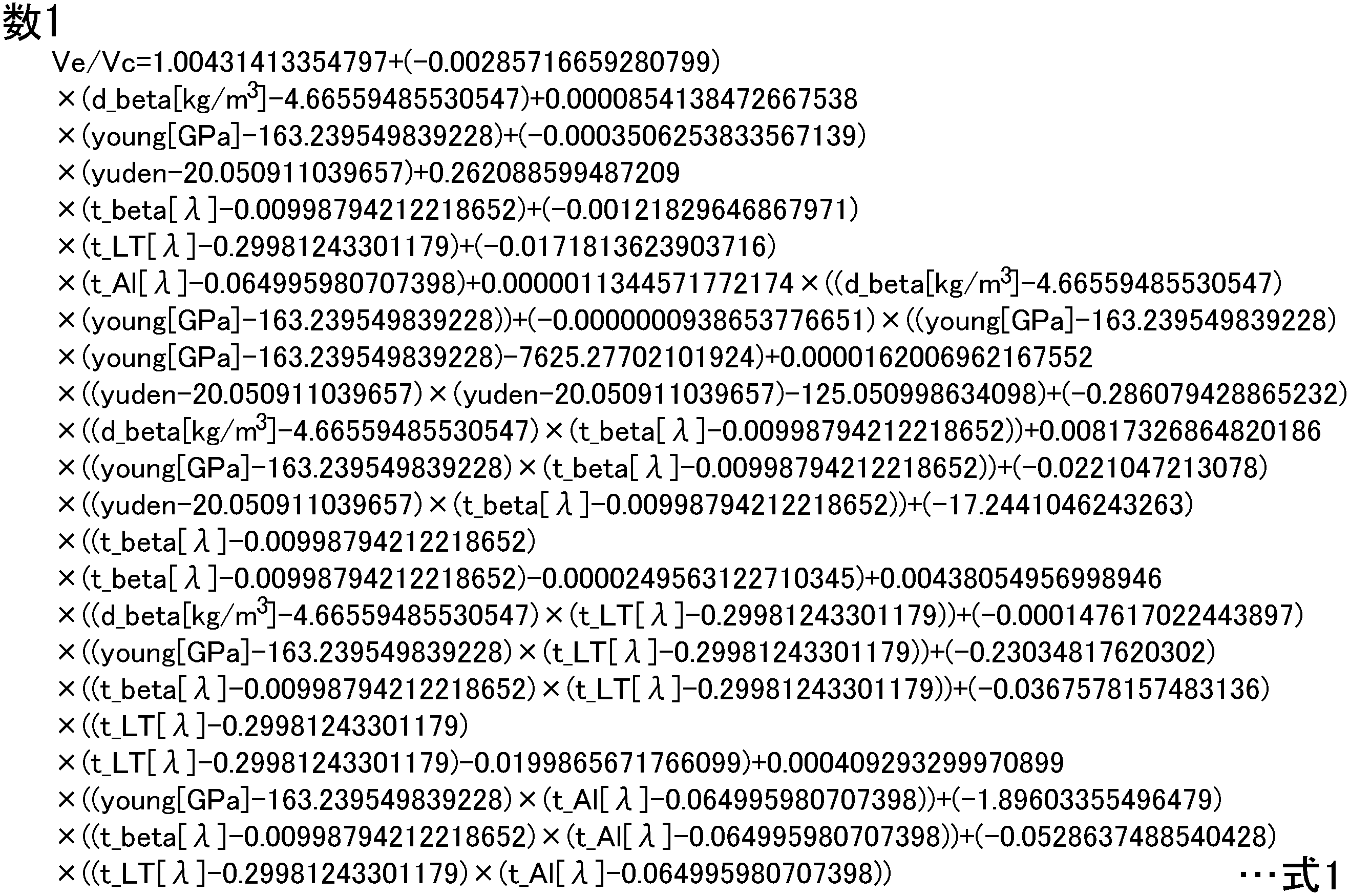
- the sound speed ratio Ve/Vc derived from Equation 1 is less than 1. More specifically, t_beta, yuden, young, d_beta, t_LT, and t_Al are preferably values within a range in which the sound speed ratio Ve/Vc derived from Equation 1 is less than one. That is, it is preferable to set the thickness of the main electrode layer of the piezoelectric layer 6 and the IDT electrode 8 and each parameter of the dielectric film 7 to a value within the range that satisfies the above conditions. As a result, the piston mode can be established more reliably and the transverse mode can be more reliably suppressed while increasing the degree of freedom in the material of the dielectric film 7 .
Landscapes
- Physics & Mathematics (AREA)
- Acoustics & Sound (AREA)
- Chemical & Material Sciences (AREA)
- Engineering & Computer Science (AREA)
- Materials Engineering (AREA)
- Surface Acoustic Wave Elements And Circuit Networks Thereof (AREA)
Abstract
材料の自由度を高めつつ、横モードを抑制することができる、弾性波装置を提供する。 本発明の弾性波装置1は、圧電体層6を含む圧電性基板2と、圧電性基板2上に設けられており、複数の電極指を有するIDT電極8と、圧電性基板2及びIDT電極8の間に設けられている誘電体膜7とを備える。IDT電極8において、弾性波伝搬方向から見たときに、隣り合う電極指が重なり合う領域が交叉領域Aである。複数の電極指が延びる方向を電極指延伸方向としたときに、交叉領域Aが、中央領域Cと、中央領域Cを電極指延伸方向において挟むように配置されている第1の領域E1及び第2の領域E2とを含む。誘電体膜7の誘電率及び密度は圧電体層6の誘電率及び密度よりも低い。誘電体膜7は、平面視において中央領域Cと重なる部分に設けられており、第1の領域E1及び第2の領域E2と重なる部分に設けられていない。
Description
本発明は、弾性波装置に関する。
従来、弾性波装置は携帯電話機のフィルタなどに広く用いられている。下記の特許文献1には、音響波装置、すなわち弾性波装置の一例が開示されている。この弾性波装置においては、圧電基板上にIDT(Interdigital Transducer)電極が設けられている。IDT電極の複数の電極指が延びる方向において、音速が異なる複数の領域が配置されている。具体的には、中央領域の外側に低音速領域が配置されており、低音速領域の外側に高音速領域が配置されている。これにより、ピストンモードを成立させることによって、横モードの抑制が図られている。
上記中央領域には、帯状の誘電体膜が配置されている。誘電体膜により、中央領域に位置する複数の電極指が覆われている。それによって、中央領域における音速が高められており、中央領域と低音速領域とにおいて音速の差が設けられている。
しかしながら、特許文献1に記載されたような、電極指の中央領域を誘電体膜で覆う構成では、中央領域の音速を高くすることができる誘電体膜は窒化ケイ素膜などに限られており、酸化ケイ素膜などを用いた場合には、音速は低くなることが知られていた。このように、ピストンモードを成立させるべく、音速を高めるために用いられる材料は限られていた。
本発明の目的は、材料の自由度を高めつつ、横モードを抑制することができる、弾性波装置を提供することにある。
本発明に係る弾性波装置は、圧電体層を含む圧電性基板と、前記圧電性基板上に設けられており、複数の電極指を有するIDT電極と、前記圧電性基板及び前記IDT電極の間に設けられている誘電体膜とを備え、前記IDT電極において、弾性波伝搬方向から見たときに、隣り合う前記電極指同士が重なり合う領域が交叉領域であり、前記複数の電極指が延びる方向を電極指延伸方向としたときに、前記交叉領域が、前記電極指延伸方向において中央に位置する中央領域と、前記中央領域を前記電極指延伸方向において挟むように配置されている第1の領域及び第2の領域とを含み、前記誘電体膜の誘電率及び密度が前記圧電体層の誘電率及び密度よりも低く、前記誘電体膜が、平面視において前記中央領域と重なる部分に設けられており、前記第1の領域及び前記第2の領域と重なる部分に設けられていない。
本発明に係る弾性波装置によれば、材料の自由度を高めつつ、横モードを抑制することができる。
以下、図面を参照しつつ、本発明の具体的な実施形態を説明することにより、本発明を明らかにする。
なお、本明細書に記載の各実施形態は、例示的なものであり、異なる実施形態間において、構成の部分的な置換または組み合わせが可能であることを指摘しておく。
図1は、本発明の第1の実施形態に係る弾性波装置の平面図である。図2は、図1中のI-I線に沿う断面図である。なお、図1及び図1以外の平面図においては、後述する誘電体膜をハッチングにより示す。
図1に示す弾性波装置1においては、ピストンモードを成立させることにより、横モードを抑制している。弾性波装置1は、圧電性基板2を有する。図2に示すように、圧電性基板2は、圧電体層6を含む積層基板である。圧電体層6上にはIDT電極8が設けられている。なお、圧電体層6及びIDT電極8の間には、誘電体膜7が設けられている。
IDT電極8に交流電圧を印加することにより、弾性波が励振される。図1に示すように、圧電体層6上における弾性波伝搬方向両側には、1対の反射器9A及び反射器9Bが設けられている。このように、本実施形態の弾性波装置1は弾性表面波共振子である。もっとも、本発明に係る弾性波装置は弾性波共振子には限定されず、複数の弾性波共振子を有するフィルタ装置やマルチプレクサであってもよい。
IDT電極8は複数の電極指を有する。IDT電極8においては、中央領域C、第1の領域E1及び第2の領域E2、並びに第1のギャップ領域G1及び第2のギャップ領域G2が配置されている。第1の領域E1及び第2の領域E2はそれぞれ、複数の電極指の先端部を含む。上記各領域における音速を異ならせることにより、ピストンモードを成立させる。
本実施形態の特徴は、弾性波装置1が以下の構成を有することにある。1)誘電体膜7の誘電率及び密度が、圧電体層6の誘電率及び密度よりも低いこと。2)誘電体膜7が、圧電性基板2及びIDT電極8の間に設けられており、かつ平面視において、中央領域Cと重なる部分に設けられており、第1の領域E1及び第2の領域E2と重なる部分に設けられていないこと。それによって、窒化ケイ素などのような限られた種類の誘電体だけでなく、他の誘電体を誘電体膜7に用いた場合においても、中央領域Cの音速を高くすることができる。よって、第1の領域E1及び第2の領域E2における音速を、中央領域Cにおける音速よりも容易に低くすることができ、ピストンモードを成立させることができる。従って、材料の自由度を高めつつ、横モードを抑制することができる。この詳細を、本実施形態の構成の詳細と共に、以下において説明する。
図2に示すように、圧電性基板2は、支持基板3と、高音速材料層としての高音速膜4と、低音速膜5と、圧電体層6とを有する。より具体的には、支持基板3上に高音速膜4が設けられている。高音速膜4上に低音速膜5が設けられている。低音速膜5上に圧電体層6が設けられている。
本実施形態においては、圧電体層6は、タンタル酸リチウム層である。一方で、誘電体膜7は、酸化ケイ素膜である。よって、誘電体膜7の誘電率及び密度は圧電体層6の誘電率及び密度よりも低い。なお、圧電体層6の材料は上記に限定されず、例えば、ニオブ酸リチウム、酸化亜鉛、窒化アルミニウム、水晶、またはPZT(チタン酸ジルコン酸鉛)などを用いることもできる。誘電体膜7の材料は上記に限定されず、例えば、窒化ケイ素または酸化アルミニウムなどを用いることもできる。誘電体膜7の誘電率及び密度が、圧電体層6の誘電率及び密度よりも低ければよい。
低音速膜5は相対的に低音速な膜である。より具体的には、低音速膜5を伝搬するバルク波の音速は、圧電体層6を伝搬するバルク波の音速よりも低い。低音速膜5の材料としては、例えば、ガラス、酸化ケイ素、酸窒化ケイ素、酸化リチウム、五酸化タンタル、または、酸化ケイ素にフッ素、炭素やホウ素を加えた化合物を主成分とする材料を用いることができる。
高音速材料層は相対的に高音速な材料である。本実施形態では、高音速材料層は高音速膜4である。高音速材料層を伝搬するバルク波の音速は、圧電体層6を伝搬する弾性波の音速よりも高い。高音速膜4の材料としては、シリコン、酸化アルミニウム、炭化ケイ素、窒化ケイ素、酸窒化ケイ素、サファイア、タンタル酸リチウム、ニオブ酸リチウム、水晶、アルミナ、ジルコニア、コージライト、ムライト、ステアタイト、フォルステライト、マグネシア、DLC(ダイヤモンドライクカーボン)膜またはダイヤモンドなど、上記材料を主成分とする媒質を用いることができる。
支持基板3の材料としては、例えば、酸化アルミニウム、タンタル酸リチウム、ニオブ酸リチウム、水晶などの圧電体、アルミナ、サファイア、マグネシア、窒化ケイ素、窒化アルミニウム、炭化ケイ素、ジルコニア、コージライト、ムライト、ステアタイト、フォルステライトなどの各種セラミック、ダイヤモンド、ガラスなどの誘電体、シリコン、窒化ガリウムなどの半導体または樹脂などを用いることができる。
図1に示すように、IDT電極8は、第1のバスバー16及び第2のバスバー17と、複数の第1の電極指18及び複数の第2の電極指19とを有する。第1のバスバー16及び第2のバスバー17は対向している。第1のバスバー16に、複数の第1の電極指18の一端がそれぞれ接続されている。第2のバスバー17に、複数の第2の電極指19の一端がそれぞれ接続されている。複数の第1の電極指18及び複数の第2の電極指19は互いに間挿し合っている。図2に示すように、誘電体膜7は、IDT電極8の圧電体層6側の面と圧電体層6との間に設けられている。なお、誘電体膜7は、第1の電極指18及び第2の電極指19の間には設けられずともよい。
ここで、複数の第1の電極指18及び複数の第2の電極指19が延びる方向を電極指延伸方向とする。本実施形態では、電極指延伸方向は、弾性波伝搬方向と直交している。IDT電極8において、弾性波伝搬方向から見たときに、隣り合う第1の電極指18及び第2の電極指19が重なり合っている部分が交叉領域Aである。交叉領域Aは、中央領域C、第1の領域E1及び上記第2の領域E2を含む。中央領域Cは、交叉領域Aにおいて、電極指延伸方向における中央側に位置している。第1の領域E1及び第2の領域E2は、中央領域Cを電極指延伸方向において挟むように配置されている。より具体的には、第1の領域E1は、中央領域Cよりも第1のバスバー16側に配置されている。第2の領域E2は、中央領域Cよりも第2のバスバー17側に配置されている。さらに、第1のギャップ領域G1が、第1の領域E1及び第1のバスバー16の間に位置する。第2のギャップ領域G2が、第2の領域E2及び第2のバスバー17の間に位置する。
IDT電極8は、積層構造を有しており、主電極層と、密着層及び保護層とを有する。圧電体層6側から、密着層、主電極層及び保護層がこの順序において積層されている。本明細書において、主電極層は、IDT電極8の質量のうち50%より大きい占有率の層をいう。本実施形態においては、密着層及び保護層は双方共にTi層であり、主電極層はAl層である。もっとも、IDT電極8の材料は上記に限定されない。あるいは、IDT電極8は主電極層のみからなっていてもよい。反射器9A及び反射器9Bには、IDT電極8と同様の材料を用いることができる。
弾性波装置1では、電極指延伸方向において、音速が異なる複数の領域が配置されている。具体的には、電極指延伸方向における中央から、中央領域C、低音速領域L1及び低音速領域L2、並びに高音速領域H1及び高音速領域H2が、この順序において配置されている。なお、低音速領域L1及び低音速領域L2は、該領域における音速が、中央領域Cにおける音速よりも低い領域である。第1の領域E1において、低音速領域L1が構成されている。第2の領域E2において、低音速領域L2が構成されている。高音速領域H1及び高音速領域H2は、該領域における音速が、中央領域Cにおける音速よりも高い領域である。第1のギャップ領域G1において高音速領域H1が構成されている。第2のギャップ領域G2において高音速領域H2が構成されている。
本実施形態では、圧電体層6及びIDT電極8の間の、平面視において中央領域Cと重なる部分に誘電体膜7が設けられている。他方、誘電体膜7は、平面視において第1の領域E1及び第2の領域E2と重なる部分には設けられていない。これにより、中央領域Cにおける音速が、第1の領域E1及び第2の領域E2における音速よりも高い。すなわち、第1の領域E1及び第2の領域E2における音速は、中央領域Cにおける音速よりも低い。他方、第1のギャップ領域G1においては、第1の電極指18及び第2の電極指19のうち第1の電極指18のみが設けられている。これにより、第1のギャップ領域G1における音速は中央領域Cにおける音速よりも高い。同様に、第2のギャップ領域G2においては、第1の電極指18及び第2の電極指19のうち第2の電極指19のみが設けられている。これにより、第2のギャップ領域G2における音速は中央領域Cにおける音速よりも高い。
ここで、中央領域Cにおける音速をVc、第1の領域E1及び第2の領域E2における音速をVe、第1のギャップ領域G1及び第2のギャップ領域G2における音速をVgとしたときに、各音速の関係はVg>Vc>Veである。なお、図1における音速の関係を示す部分においては、矢印Vで示すように、各音速の高さを示す線が左側に位置するほど音速が高いことを示す。電極指延伸方向における中央から、中央領域C、低音速領域L1及び低音速領域L2、並びに高音速領域H1及び高音速領域H2が、この順序において配置されている。それによって、ピストンモードを成立させる。
本開示では、上記のように、圧電体層6及びIDT電極8の間の、平面視において中央領域Cと重なる部分に誘電体膜7を設けることにより、中央領域Cにおける音速を高くできる。この詳細を以下において示す。
第1の実施形態と同様の構成を有する弾性波装置、並びに第1の比較例及び第2の比較例における中央領域の音速と、誘電体膜の厚みとの関係を求めた。より具体的には、第1の実施形態と同様の構成を有する弾性波装置の誘電体膜を、酸化ケイ素膜とした場合及び窒化ケイ素膜とした場合の双方において上記関係を求めた。第1の比較例においては、第1の実施形態と同様の位置に設けられた誘電体膜を五酸化タンタル膜とした。五酸化タンタル膜の密度は、圧電体層としてのタンタル酸リチウム層の密度よりも高い。第2の比較例においては、図3に示すように、誘電体膜107が、IDT電極8を覆うように設けられている。誘電体膜107は酸化ケイ素膜とした。さらに、第3の比較例として、誘電体膜を設けない場合の中央領域における音速も求めた。上記各弾性波装置の設計パラメータは以下の通りである。なお、IDT電極の電極指ピッチにより規定される波長をλとする。電極指ピッチとは、隣り合う電極指同士の中心間距離である。
支持基板;材料…Si
高音速膜;材料…SiN、厚み…300nm
低音速膜;材料…SiO2、厚み…300nm
圧電体層;材料…55°YカットLiTaO3、厚み…400nm
IDT電極;各層の材料…圧電体層側からTi/Al/Ti、厚み…12nm/100nm/4nm、波長λ…2μm、デューティ比…0.5
高音速膜;材料…SiN、厚み…300nm
低音速膜;材料…SiO2、厚み…300nm
圧電体層;材料…55°YカットLiTaO3、厚み…400nm
IDT電極;各層の材料…圧電体層側からTi/Al/Ti、厚み…12nm/100nm/4nm、波長λ…2μm、デューティ比…0.5
なお、誘電体膜の厚みは、それぞれ5nm以上、55nm以下の範囲において10nm刻みで変化させた。第3の比較例では、誘電体膜の厚みは0である。
図4は、IDT電極の中央領域における誘電体膜の厚みと音速との関係を示す図である。
図4に示すように、第1の比較例及び第2の比較例においては、誘電体膜の厚みが厚くなるほど、中央領域における音速Vcが低くなっていることがわかる。第1の比較例のように、誘電体膜の密度が圧電体層の密度よりも高い場合には、誘電体膜の位置及び厚みを第1の実施形態と同様としても、音速Vcは低くなる。第2の比較例が示す従来の例のように、酸化ケイ素膜を、IDT電極を覆うように設けた場合にも、音速Vcは低くなる。
これらに対して、第1の実施形態においては、誘電体膜7の厚みが厚くなるほど、中央領域Cにおける音速Vcが高くなっている。特に、従来では音速を低くすると考えられていた酸化ケイ素膜を用いた場合においても、音速Vcを高くすることができている。これにより、図1に示すように、中央領域Cと、第1の領域E1及び第2の領域E2との間において音速の差を設けることができ、ピストンモードを成立させることができる。このように、材料の自由度を高めつつ、横モードを抑制することができる。
これは、以下の理由によるものと考えられる。圧電体層6及びIDT電極8の間に、誘電率及び密度が低い誘電体膜7が設けられている場合には、電界強度が低くなり、電気機械結合係数が小さくなる。これにより、比帯域の値が小さくなる。これは、共振周波数が高くなることと同義といえる。共振周波数をf、IDT電極の電極指ピッチにより規定される波長をλ、音速をvとしたときに、f=v/λである。電極指ピッチは一定であり、波長λは一定であるため、共振周波数fが高くなると、音速vも高くなる。よって、圧電体層6及びIDT電極8の間に、誘電率及び密度が圧電体層6よりも低い誘電体膜7が設けられると、音速が高くなる効果があるといえる。以下において、第1の実施形態の中央領域Cにおいて、共振周波数が高くなることを示す。さらに、第2の比較例のように、中央領域Cにおいて誘電体膜107がIDT電極8を覆っている場合と、第1の実施形態とを比較する。
図5は、第1の実施形態及び第2の比較例の、中央領域及び第1の領域におけるインピーダンス周波数特性を示す図である。なお、第1の領域E1の構成は、第1の実施形態及び第2の比較例において同様である。そのため、第1の実施形態及び第2の比較例における第1の領域E1の結果を、同じ一点鎖線により示している。
図5に示すように、第2の比較例においては、破線で示す中央領域Cにおける共振周波数は、一点鎖線で示す第1の領域E1における共振周波数よりも低くなっている。そのため、中央領域Cの音速が第1の領域E1における音速よりも低く、ピストンモードは成立しない。
これに対して、第1の実施形態においては、実線で示す中央領域Cにおける共振周波数は、第1の領域E1における音速よりも高くなっていることがわかる。なお、図示しないが、中央領域Cと第2の領域E2との音速の関係も同様である。上記のように、第1の実施形態及び第2の比較例においては、誘電体膜には酸化ケイ素膜が用いられている。そして、第2の比較例においてはピストンモードが成立しない一方で、第1の実施形態ではピストンモードを成立させることができる。このように、第1の実施形態では、材料の自由度を高めつつ、横モードを抑制することができる。
ところで、図2に示すように、圧電性基板2においては、高音速膜4、低音速膜5及び圧電体層6がこの順序において積層されている。それによって、弾性波のエネルギーを圧電体層6側に効果的に閉じ込めることができる。もっとも、圧電性基板2の構成は上記に限定されない。以下において、圧電性基板の構成のみが第1の実施形態と異なる、第1の実施形態の第1の変形例及び第2の変形例を示す。第1の変形例及び第2の変形例においても、第1の実施形態と同様に、材料の自由度を高めつつ、横モードを抑制することができる。さらに、弾性波のエネルギーを圧電体層6側に効果的に閉じ込めることができる。
図6に示す第1の変形例においては、高音速材料層は高音速支持基板24である。圧電性基板22Aは、高音速支持基板24と、低音速膜5と、圧電体層6とを有する。より具体的には、高音速支持基板24上に低音速膜5が設けられている。低音速膜5上に圧電体層6が設けられている。本変形例においても、第1の実施形態と同様に、圧電体層6は、高音速材料層上に低音速膜5を介して間接的に設けられている。
図7に示す第2の変形例においては、圧電性基板22Bは、支持基板3と、高音速膜4と、圧電体層6とを有する。より具体的には、支持基板3上に高音速膜4が設けられている。高音速膜4上に圧電体層6が設けられている。本変形例では、圧電体層6は、高音速材料層上に直接的に設けられている。
なお、圧電性基板は、高音速支持基板24及び圧電体層6の積層体であってもよく、高音速支持基板24、低音速膜5及び圧電体層6の積層体であってもよい。あるいは、圧電性基板は、圧電体層6のみからなる圧電基板であってもよい。
ここで、圧電体層6がタンタル酸リチウム層であり、IDT電極8の主電極層がAl層であり、誘電体膜7が任意の誘電体からなる場合において、弾性波装置1の各パラメータと音速比Ve/Vcとの関係を求めた。なお、音速比Ve/Vcは、第1の領域E1及び第2の領域E2における音速Veの、中央領域Cにおける音速Vcに対する比である。上記各パラメータとして、誘電体膜7の厚みをt_beta[λ]、誘電体膜7の誘電率をyuden、誘電体膜7のヤング率をyoung[GPa]、誘電体膜7の密度をd_beta[kg/m3]とする。t_beta、yuden、young及びd_betaをそれぞれ変化させて、音速比Ve/Vcを測定した。上記測定を行った弾性波装置1の設計パラメータは以下の通りである。
支持基板3;材料…Si
高音速膜4;材料…SiN、厚み…300nm
低音速膜5;材料…SiO2、厚み…300nm
圧電体層6;材料…55°YカットLiTaO3、厚み…400nm
IDT電極8;各層の材料…圧電体層6側からTi/Al/Ti、厚み…12nm/100nm/4nm、波長λ…2μm、デューティ比…0.5
高音速膜4;材料…SiN、厚み…300nm
低音速膜5;材料…SiO2、厚み…300nm
圧電体層6;材料…55°YカットLiTaO3、厚み…400nm
IDT電極8;各層の材料…圧電体層6側からTi/Al/Ti、厚み…12nm/100nm/4nm、波長λ…2μm、デューティ比…0.5
上記測定により、各パラメータと音速比Ve/Vcとの関係を求めた。図8~図10において、誘電体膜7の各パラメータと、音速比Ve/Vcとの関係を示す。
図8は、誘電体膜の厚み及び密度と、音速比Ve/Vcとの関係を示す図である。図9は、誘電体膜の厚み及びヤング率と、音速比Ve/Vcとの関係を示す図である。図10は、誘電体膜の厚み及び誘電率と、音速比Ve/Vcとの関係を示す図である。図8~図10中の各曲線がそれぞれ、一定の音速比Ve/Vcとなる各パラメータの関係を示す。
図8~図10におけるハッチングにより示す領域が、Ve/Vc<1の領域である。これらの領域内において、ピストンモードをより確実に成立させることができる。よって、用いる誘電体膜7の各パラメータをこれらの領域の範囲内の値とすることにより、ピストンモードをより確実に成立させることができ、横モードをより確実に抑制することができる。
さらに、圧電体層6の厚みをt_LT[λ]、IDT電極8の主電極層の厚みをt_Al[λ]とする。t_LT、t_Al、t_beta、yuden、young及びd_betaをそれぞれ変化させて、音速比Ve/Vcを測定した。上記測定を行った弾性波装置1の設計パラメータは以下の通りである。
支持基板3;材料…Si
高音速膜4;材料…SiN、厚み…300nm
低音速膜5;材料…SiO2、厚み…300nm
圧電体層6;材料…55°YカットLiTaO3、厚み…t_LT
IDT電極8;各層の材料…圧電体層6側からTi/Al/Ti、厚み…12nm/t_Al/4nm、波長λ…2μm、デューティ比…0.5
高音速膜4;材料…SiN、厚み…300nm
低音速膜5;材料…SiO2、厚み…300nm
圧電体層6;材料…55°YカットLiTaO3、厚み…t_LT
IDT電極8;各層の材料…圧電体層6側からTi/Al/Ti、厚み…12nm/t_Al/4nm、波長λ…2μm、デューティ比…0.5
誘電体膜7の厚みt_beta;0.0025λ以上、0.0175λの範囲において、0.0025λ刻みで変化させた。
誘電体膜7の誘電率yuden;5以上、35以下の範囲において、5刻みで変化させた。
誘電体膜7のヤング率young;70GPa以上、280GPa以下の範囲において、70GPa刻みで変化させた。
誘電体膜7の密度d_beta;2kg/m3以上、8kg/m3以下の範囲において、2kg/m3刻みで変化させた。
圧電体層6の厚みt_LT;0.15λ以上、0.3λ以下の範囲において、0.05λ刻みで変化させた。
IDT電極の主電極層の厚みt_Al;0.05λ以上、0.075λの範囲において、0.0125λ刻みで変化させた。
上記測定により、各パラメータと音速比Ve/Vcとの関係式である式1を導出した。

式1により導出される音速比Ve/Vcが1未満であることが好ましい。より具体的には、t_beta、yuden、young、d_beta、t_LT及びt_Alが、式1により導出される音速比Ve/Vcが1未満となる範囲内の値であることが好ましい。すなわち、圧電体層6及びIDT電極8の主電極層の厚み、並びに誘電体膜7の各パラメータを上記条件を満たす範囲内の値とすることが好ましい。これにより、誘電体膜7の材料の自由度を高めつつ、ピストンモードをより確実に成立させることができ、横モードをより確実に抑制することができる。
1…弾性波装置
2…圧電性基板
3…支持基板
4…高音速膜
5…低音速膜
6…圧電体層
7…誘電体膜
8…IDT電極
9A,9B…反射器
16,17…第1,第2のバスバー
18,19…第1,第2の電極指
22A,22B…圧電性基板
24…高音速支持基板
107…誘電体膜
A…交叉領域
C…中央領域
E1,E2…第1,第2の領域
G1,G2…第1,第2のギャップ領域
H1,H2…高音速領域
L1,L2…低音速領域
2…圧電性基板
3…支持基板
4…高音速膜
5…低音速膜
6…圧電体層
7…誘電体膜
8…IDT電極
9A,9B…反射器
16,17…第1,第2のバスバー
18,19…第1,第2の電極指
22A,22B…圧電性基板
24…高音速支持基板
107…誘電体膜
A…交叉領域
C…中央領域
E1,E2…第1,第2の領域
G1,G2…第1,第2のギャップ領域
H1,H2…高音速領域
L1,L2…低音速領域
Claims (7)
- 圧電体層を含む圧電性基板と、
前記圧電性基板上に設けられており、複数の電極指を有するIDT電極と、
前記圧電性基板及び前記IDT電極の間に設けられている誘電体膜と、
を備え、
前記IDT電極において、弾性波伝搬方向から見たときに、隣り合う前記電極指同士が重なり合う領域が交叉領域であり、前記複数の電極指が延びる方向を電極指延伸方向としたときに、前記交叉領域が、前記電極指延伸方向において中央に位置する中央領域と、前記中央領域を前記電極指延伸方向において挟むように配置されている第1の領域及び第2の領域と、を含み、
前記誘電体膜の誘電率及び密度が前記圧電体層の誘電率及び密度よりも低く、
前記誘電体膜が、平面視において前記中央領域と重なる部分に設けられており、前記第1の領域及び前記第2の領域と重なる部分に設けられていない、弾性波装置。 - 前記誘電体膜が、酸化ケイ素膜、窒化ケイ素膜または酸化アルミニウム膜である、請求項1に記載の弾性波装置。
- 前記圧電性基板が、高音速材料層を有し、前記高音速材料層上に前記圧電体層が設けられており、
前記高音速材料層を伝搬するバルク波の音速が、前記圧電体層を伝搬する弾性波の音速よりも高い、請求項1または2に記載の弾性波装置。 - 前記圧電性基板が、前記高音速材料層と前記圧電体層との間に設けられている、低音速膜を有し、
前記低音速膜を伝搬するバルク波の音速が、前記圧電体層を伝搬するバルク波の音速よりも低い、請求項3に記載の弾性波装置。 - 前記高音速材料層が高音速支持基板である、請求項3または4に記載の弾性波装置。
- 前記圧電性基板が支持基板を有し、
前記高音速材料層が、前記支持基板上に設けられている高音速膜である、請求項3または4に記載の弾性波装置。 - 前記圧電体層がタンタル酸リチウム層であり、
前記IDT電極が主電極層を有し、前記主電極層がAl層であり、
前記IDT電極の電極指ピッチにより規定される波長をλとし、前記誘電体膜の厚みをt_beta[λ]、前記誘電体膜の誘電率をyuden、前記誘電体膜のヤング率をyoung[GPa]、前記誘電体膜の密度をd_beta[kg/m3]、前記圧電体層の厚みをt_LT[λ]、前記IDT電極の前記主電極層の厚みをt_Al[λ]とし、前記第1の領域及び前記第2の領域における音速をVe、前記中央領域における音速をVcとしたときに、前記t_beta、前記yuden、前記young、前記d_beta、前記t_LT及び前記t_Alが、下記の式1により導出される音速比Ve/Vcが1未満となる範囲内の値である、請求項1~6のいずれか1項に記載の弾性波装置。
Priority Applications (2)
| Application Number | Priority Date | Filing Date | Title |
|---|---|---|---|
| CN202280008025.9A CN116636141A (zh) | 2021-01-19 | 2022-01-13 | 弹性波装置 |
| US18/200,012 US20230308079A1 (en) | 2021-01-19 | 2023-05-22 | Acoustic wave device |
Applications Claiming Priority (2)
| Application Number | Priority Date | Filing Date | Title |
|---|---|---|---|
| JP2021-006432 | 2021-01-19 | ||
| JP2021006432 | 2021-01-19 |
Related Child Applications (1)
| Application Number | Title | Priority Date | Filing Date |
|---|---|---|---|
| US18/200,012 Continuation US20230308079A1 (en) | 2021-01-19 | 2023-05-22 | Acoustic wave device |
Publications (1)
| Publication Number | Publication Date |
|---|---|
| WO2022158363A1 true WO2022158363A1 (ja) | 2022-07-28 |
Family
ID=82548958
Family Applications (1)
| Application Number | Title | Priority Date | Filing Date |
|---|---|---|---|
| PCT/JP2022/000840 Ceased WO2022158363A1 (ja) | 2021-01-19 | 2022-01-13 | 弾性波装置 |
Country Status (3)
| Country | Link |
|---|---|
| US (1) | US20230308079A1 (ja) |
| CN (1) | CN116636141A (ja) |
| WO (1) | WO2022158363A1 (ja) |
Families Citing this family (2)
| Publication number | Priority date | Publication date | Assignee | Title |
|---|---|---|---|---|
| WO2021210551A1 (ja) * | 2020-04-17 | 2021-10-21 | 株式会社村田製作所 | 弾性波装置 |
| US12341489B2 (en) * | 2021-09-13 | 2025-06-24 | Rf360 Singapore Pte. Ltd. | Surface-acoustic-wave (SAW) filter with a compensation layer having multiple densities |
Citations (2)
| Publication number | Priority date | Publication date | Assignee | Title |
|---|---|---|---|---|
| JP2012186808A (ja) * | 2011-03-07 | 2012-09-27 | Triquint Semiconductor Inc | トリミング効果とピストンモードでの不安定性を最小化する音響波導波装置および方法 |
| WO2019138813A1 (ja) * | 2018-01-12 | 2019-07-18 | 株式会社村田製作所 | 弾性波装置、マルチプレクサ、高周波フロントエンド回路、及び通信装置 |
-
2022
- 2022-01-13 CN CN202280008025.9A patent/CN116636141A/zh active Pending
- 2022-01-13 WO PCT/JP2022/000840 patent/WO2022158363A1/ja not_active Ceased
-
2023
- 2023-05-22 US US18/200,012 patent/US20230308079A1/en active Pending
Patent Citations (2)
| Publication number | Priority date | Publication date | Assignee | Title |
|---|---|---|---|---|
| JP2012186808A (ja) * | 2011-03-07 | 2012-09-27 | Triquint Semiconductor Inc | トリミング効果とピストンモードでの不安定性を最小化する音響波導波装置および方法 |
| WO2019138813A1 (ja) * | 2018-01-12 | 2019-07-18 | 株式会社村田製作所 | 弾性波装置、マルチプレクサ、高周波フロントエンド回路、及び通信装置 |
Also Published As
| Publication number | Publication date |
|---|---|
| CN116636141A (zh) | 2023-08-22 |
| US20230308079A1 (en) | 2023-09-28 |
Similar Documents
| Publication | Publication Date | Title |
|---|---|---|
| US20220216842A1 (en) | Acoustic wave device and filter device | |
| CN112997403B (zh) | 弹性波装置 | |
| US10659001B2 (en) | Elastic wave device | |
| WO2023002858A1 (ja) | 弾性波装置及びフィルタ装置 | |
| CN114467256A (zh) | 弹性波装置 | |
| WO2020171050A1 (ja) | 弾性波装置 | |
| US20230084340A1 (en) | Acoustic wave device | |
| US20220224311A1 (en) | Acoustic wave device | |
| US20240154595A1 (en) | Acoustic wave device | |
| WO2021200835A1 (ja) | 弾性波装置 | |
| WO2022019170A1 (ja) | 弾性波装置 | |
| WO2022054773A1 (ja) | 弾性波装置 | |
| US20230308079A1 (en) | Acoustic wave device | |
| US20240213949A1 (en) | Acoustic wave device | |
| US20230275560A1 (en) | Acoustic wave device | |
| WO2021220887A1 (ja) | 弾性波装置 | |
| CN115485973B (zh) | 弹性波装置 | |
| US20250167760A1 (en) | Acoustic wave device | |
| US20250119114A1 (en) | Acoustic wave device | |
| WO2022124391A1 (ja) | 弾性波装置 | |
| US20240014793A1 (en) | Acoustic wave device and method for manufacturing acoustic wave device | |
| WO2023048140A1 (ja) | 弾性波装置 | |
| WO2023002824A1 (ja) | 弾性波装置 | |
| WO2022138328A1 (ja) | 弾性波装置 | |
| WO2022071488A1 (ja) | 弾性波装置 |
Legal Events
| Date | Code | Title | Description |
|---|---|---|---|
| 121 | Ep: the epo has been informed by wipo that ep was designated in this application |
Ref document number: 22742485 Country of ref document: EP Kind code of ref document: A1 |
|
| WWE | Wipo information: entry into national phase |
Ref document number: 202280008025.9 Country of ref document: CN |
|
| NENP | Non-entry into the national phase |
Ref country code: DE |
|
| 122 | Ep: pct application non-entry in european phase |
Ref document number: 22742485 Country of ref document: EP Kind code of ref document: A1 |
|
| NENP | Non-entry into the national phase |
Ref country code: JP |