WO2022158482A1 - 光学積層体および画像表示装置 - Google Patents
光学積層体および画像表示装置 Download PDFInfo
- Publication number
- WO2022158482A1 WO2022158482A1 PCT/JP2022/001758 JP2022001758W WO2022158482A1 WO 2022158482 A1 WO2022158482 A1 WO 2022158482A1 JP 2022001758 W JP2022001758 W JP 2022001758W WO 2022158482 A1 WO2022158482 A1 WO 2022158482A1
- Authority
- WO
- WIPO (PCT)
- Prior art keywords
- layer
- retardation
- film
- liquid crystal
- optical laminate
- Prior art date
- Legal status (The legal status is an assumption and is not a legal conclusion. Google has not performed a legal analysis and makes no representation as to the accuracy of the status listed.)
- Ceased
Links
Images


Classifications
-
- G—PHYSICS
- G02—OPTICS
- G02B—OPTICAL ELEMENTS, SYSTEMS OR APPARATUS
- G02B5/00—Optical elements other than lenses
- G02B5/30—Polarising elements
- G02B5/3016—Polarising elements involving passive liquid crystal elements
-
- B—PERFORMING OPERATIONS; TRANSPORTING
- B32—LAYERED PRODUCTS
- B32B—LAYERED PRODUCTS, i.e. PRODUCTS BUILT-UP OF STRATA OF FLAT OR NON-FLAT, e.g. CELLULAR OR HONEYCOMB, FORM
- B32B27/00—Layered products comprising a layer of synthetic resin
-
- B—PERFORMING OPERATIONS; TRANSPORTING
- B32—LAYERED PRODUCTS
- B32B—LAYERED PRODUCTS, i.e. PRODUCTS BUILT-UP OF STRATA OF FLAT OR NON-FLAT, e.g. CELLULAR OR HONEYCOMB, FORM
- B32B7/00—Layered products characterised by the relation between layers; Layered products characterised by the relative orientation of features between layers, or by the relative values of a measurable parameter between layers, i.e. products comprising layers having different physical, chemical or physicochemical properties; Layered products characterised by the interconnection of layers
- B32B7/02—Physical, chemical or physicochemical properties
- B32B7/023—Optical properties
-
- C—CHEMISTRY; METALLURGY
- C09—DYES; PAINTS; POLISHES; NATURAL RESINS; ADHESIVES; COMPOSITIONS NOT OTHERWISE PROVIDED FOR; APPLICATIONS OF MATERIALS NOT OTHERWISE PROVIDED FOR
- C09J—ADHESIVES; NON-MECHANICAL ASPECTS OF ADHESIVE PROCESSES IN GENERAL; ADHESIVE PROCESSES NOT PROVIDED FOR ELSEWHERE; USE OF MATERIALS AS ADHESIVES
- C09J201/00—Adhesives based on unspecified macromolecular compounds
-
- C—CHEMISTRY; METALLURGY
- C09—DYES; PAINTS; POLISHES; NATURAL RESINS; ADHESIVES; COMPOSITIONS NOT OTHERWISE PROVIDED FOR; APPLICATIONS OF MATERIALS NOT OTHERWISE PROVIDED FOR
- C09J—ADHESIVES; NON-MECHANICAL ASPECTS OF ADHESIVE PROCESSES IN GENERAL; ADHESIVE PROCESSES NOT PROVIDED FOR ELSEWHERE; USE OF MATERIALS AS ADHESIVES
- C09J7/00—Adhesives in the form of films or foils
- C09J7/20—Adhesives in the form of films or foils characterised by their carriers
- C09J7/22—Plastics; Metallised plastics
- C09J7/24—Plastics; Metallised plastics based on macromolecular compounds obtained by reactions involving only carbon-to-carbon unsaturated bonds
-
- C—CHEMISTRY; METALLURGY
- C09—DYES; PAINTS; POLISHES; NATURAL RESINS; ADHESIVES; COMPOSITIONS NOT OTHERWISE PROVIDED FOR; APPLICATIONS OF MATERIALS NOT OTHERWISE PROVIDED FOR
- C09J—ADHESIVES; NON-MECHANICAL ASPECTS OF ADHESIVE PROCESSES IN GENERAL; ADHESIVE PROCESSES NOT PROVIDED FOR ELSEWHERE; USE OF MATERIALS AS ADHESIVES
- C09J7/00—Adhesives in the form of films or foils
- C09J7/20—Adhesives in the form of films or foils characterised by their carriers
- C09J7/29—Laminated material
-
- C—CHEMISTRY; METALLURGY
- C09—DYES; PAINTS; POLISHES; NATURAL RESINS; ADHESIVES; COMPOSITIONS NOT OTHERWISE PROVIDED FOR; APPLICATIONS OF MATERIALS NOT OTHERWISE PROVIDED FOR
- C09J—ADHESIVES; NON-MECHANICAL ASPECTS OF ADHESIVE PROCESSES IN GENERAL; ADHESIVE PROCESSES NOT PROVIDED FOR ELSEWHERE; USE OF MATERIALS AS ADHESIVES
- C09J7/00—Adhesives in the form of films or foils
- C09J7/30—Adhesives in the form of films or foils characterised by the adhesive composition
- C09J7/38—Pressure-sensitive adhesives [PSA]
-
- G—PHYSICS
- G02—OPTICS
- G02B—OPTICAL ELEMENTS, SYSTEMS OR APPARATUS
- G02B5/00—Optical elements other than lenses
- G02B5/30—Polarising elements
-
- G—PHYSICS
- G02—OPTICS
- G02B—OPTICAL ELEMENTS, SYSTEMS OR APPARATUS
- G02B5/00—Optical elements other than lenses
- G02B5/30—Polarising elements
- G02B5/3083—Birefringent or phase retarding elements
-
- G—PHYSICS
- G02—OPTICS
- G02F—OPTICAL DEVICES OR ARRANGEMENTS FOR THE CONTROL OF LIGHT BY MODIFICATION OF THE OPTICAL PROPERTIES OF THE MEDIA OF THE ELEMENTS INVOLVED THEREIN; NON-LINEAR OPTICS; FREQUENCY-CHANGING OF LIGHT; OPTICAL LOGIC ELEMENTS; OPTICAL ANALOGUE/DIGITAL CONVERTERS
- G02F1/00—Devices or arrangements for the control of the intensity, colour, phase, polarisation or direction of light arriving from an independent light source, e.g. switching, gating or modulating; Non-linear optics
- G02F1/01—Devices or arrangements for the control of the intensity, colour, phase, polarisation or direction of light arriving from an independent light source, e.g. switching, gating or modulating; Non-linear optics for the control of the intensity, phase, polarisation or colour
- G02F1/13—Devices or arrangements for the control of the intensity, colour, phase, polarisation or direction of light arriving from an independent light source, e.g. switching, gating or modulating; Non-linear optics for the control of the intensity, phase, polarisation or colour based on liquid crystals, e.g. single liquid crystal display cells
- G02F1/133—Constructional arrangements; Operation of liquid crystal cells; Circuit arrangements
- G02F1/1333—Constructional arrangements; Manufacturing methods
- G02F1/1335—Structural association of cells with optical devices, e.g. polarisers or reflectors
-
- G—PHYSICS
- G02—OPTICS
- G02F—OPTICAL DEVICES OR ARRANGEMENTS FOR THE CONTROL OF LIGHT BY MODIFICATION OF THE OPTICAL PROPERTIES OF THE MEDIA OF THE ELEMENTS INVOLVED THEREIN; NON-LINEAR OPTICS; FREQUENCY-CHANGING OF LIGHT; OPTICAL LOGIC ELEMENTS; OPTICAL ANALOGUE/DIGITAL CONVERTERS
- G02F1/00—Devices or arrangements for the control of the intensity, colour, phase, polarisation or direction of light arriving from an independent light source, e.g. switching, gating or modulating; Non-linear optics
- G02F1/01—Devices or arrangements for the control of the intensity, colour, phase, polarisation or direction of light arriving from an independent light source, e.g. switching, gating or modulating; Non-linear optics for the control of the intensity, phase, polarisation or colour
- G02F1/13—Devices or arrangements for the control of the intensity, colour, phase, polarisation or direction of light arriving from an independent light source, e.g. switching, gating or modulating; Non-linear optics for the control of the intensity, phase, polarisation or colour based on liquid crystals, e.g. single liquid crystal display cells
- G02F1/133—Constructional arrangements; Operation of liquid crystal cells; Circuit arrangements
- G02F1/1333—Constructional arrangements; Manufacturing methods
- G02F1/1335—Structural association of cells with optical devices, e.g. polarisers or reflectors
- G02F1/13363—Birefringent elements, e.g. for optical compensation
-
- G—PHYSICS
- G09—EDUCATION; CRYPTOGRAPHY; DISPLAY; ADVERTISING; SEALS
- G09F—DISPLAYING; ADVERTISING; SIGNS; LABELS OR NAME-PLATES; SEALS
- G09F9/00—Indicating arrangements for variable information in which the information is built-up on a support by selection or combination of individual elements
-
- H—ELECTRICITY
- H05—ELECTRIC TECHNIQUES NOT OTHERWISE PROVIDED FOR
- H05B—ELECTRIC HEATING; ELECTRIC LIGHT SOURCES NOT OTHERWISE PROVIDED FOR; CIRCUIT ARRANGEMENTS FOR ELECTRIC LIGHT SOURCES, IN GENERAL
- H05B33/00—Electroluminescent light sources
- H05B33/02—Details
-
- H—ELECTRICITY
- H10—SEMICONDUCTOR DEVICES; ELECTRIC SOLID-STATE DEVICES NOT OTHERWISE PROVIDED FOR
- H10K—ORGANIC ELECTRIC SOLID-STATE DEVICES
- H10K59/00—Integrated devices, or assemblies of multiple devices, comprising at least one organic light-emitting element covered by group H10K50/00
- H10K59/80—Constructional details
- H10K59/87—Passivation; Containers; Encapsulations
- H10K59/871—Self-supporting sealing arrangements
- H10K59/8722—Peripheral sealing arrangements, e.g. adhesives, sealants
Definitions
- the present invention relates to an optical laminate and an image display device.
- the present invention relates to an optical laminate and an image display device having a retardation layer containing a cycloolefin polymer film and an adhesive layer.
- IPS In-Plane Switching
- FFS Ringe Field Switching
- TN Transmission Nematic
- VA Very Alignment
- an electric field is applied between the upper and lower substrates, This mode is called a horizontal electric field method in which the liquid crystal molecules respond in the in-plane direction of the substrate by an electric field containing a component almost parallel to the substrate plane, instead of the mode driven by the rise of the liquid crystal molecules.
- the IPS type and FFS type liquid crystal display devices have the characteristics of a wide viewing angle and little chromaticity shift and color tone change, because they are in principle less restrictive to the viewing angle due to their structure. Known as drive system.
- Patent Literature 1 discloses a wide-viewing-angle lateral electric field type liquid crystal display device in which an optically anisotropic layer is arranged so that the optical compensation of the display device as a whole is studied.
- a retardation layer using a cycloolefin polymer as a base material is used for the purpose of improving display performance changes due to changes in the temperature and humidity environment of the usage environment. It has been known.
- the present inventors have investigated the durability of a liquid crystal display device having such a retardation layer, and found that there is no problem when used for general PC (personal computer) monitors and television applications. It was clarified that there is room for improvement when using it for outdoor signage, industrial use, vehicle use, etc.
- an object of the present invention is to provide an optical layered body having excellent durability and an image display device using the same.
- the present inventors have found that the organic low-molecular weight component contained in the pressure-sensitive adhesive layer in contact with the retardation layer containing the cycloolefin polymer affects the durability. .
- the present inventors have found that the above problems can be solved by providing an intermediate layer between the retardation layer and the pressure-sensitive adhesive layer, or by reducing the content of the organic low-molecular-weight components contained in the pressure-sensitive adhesive layer. He found the headline and completed the present invention. That is, the inventors have found that the above object can be achieved by the following configuration.
- the pressure-sensitive adhesive layer contains an organic low-molecular-weight component with a molecular weight of 500 or less, and the content of the organic low-molecular-weight component with a molecular weight of 500 or less is 2.6% by mass or less, or the retardation layer and the pressure-sensitive adhesive layer is in direct contact with and adhered to the glass substrate via the adhesive layer, and a durability test is performed at 115 ° C. for 100 hours.
- the content of the molecular component is 50% or less of the content before the durability test.
- Condition III The in-plane retardation Re(550) at a wavelength of 550 nm and the thickness direction retardation Rth(550) of the total retardation layer satisfy the following formulas (1) and (2), respectively. .
- An image display device comprising the optical laminate according to any one of [1] to [9].
- FIG. 1 is a schematic cross-sectional view of a conventional liquid crystal image display device;
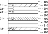
- FIG. 1 is a schematic cross-sectional view of an embodiment of an image display device of the present invention;
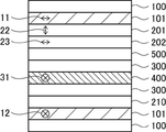
- FIG. 4 is a schematic cross-sectional view of another embodiment of the image display device of the present invention;
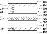
- FIG. 4 is a schematic cross-sectional view of another embodiment of the image display device of the present invention;
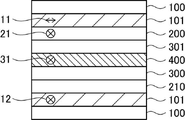
- FIG. 4 is a schematic cross-sectional view of another embodiment of the image display device of the present invention;
- FIG. 4 is a schematic cross-sectional view of another embodiment of the image display device of the present invention;
- a numerical range represented by "-" means a range including the numerical values before and after "-" as lower and upper limits.
- parallel, orthogonal, horizontal, and vertical do not mean parallel, orthogonal, horizontal, and vertical in a strict sense, respectively, but within a range of parallel ⁇ 10 °, It means a range of ⁇ 10° orthogonal, ⁇ 10° horizontal, and ⁇ 10° vertical.
- Re( ⁇ ) and Rth( ⁇ ) respectively represent in-plane retardation and thickness direction retardation at wavelength ⁇ . If the wavelength ⁇ of retardation is not specified, the wavelength ⁇ is assumed to be 550 nm.
- the refractive indices nx and ny are the refractive indices in the in-plane direction of the optical member. is the refractive index in the direction perpendicular to the phase axis).
- nz is the refractive index in the thickness direction.
- NAR-4T Abbe refractometer
- DR-M2 manufactured by Atago Co., Ltd.
- the values in the polymer handbook (JOHN WILEY & SONS, INC) and various optical film catalogs can also be used.
- each component may use the substance applicable to each component individually by 1 type, or may use 2 or more types together.
- the content of the component refers to the total content of the substances used in combination unless otherwise specified.
- (meth)acrylate” is a notation representing “acrylate” or “methacrylate”
- (meth)acryl is a notation representing "acrylic” or “methacrylic”
- (Meth)acryloyl” is a notation representing “acryloyl” or “methacryloyl”.
- optical laminate of the present invention has a polarizer, a retardation layer containing a cycloolefin-based polymer film, and an adhesive layer in this order, and the polarizer is provided on at least one side. It has a protective layer.
- at least one side refers to at least one of the surface of the polarizer on the side of the retardation layer and the surface of the polarizer on the side opposite to the retardation layer.
- the optical laminate of the present invention satisfies the following conditions I and III, or conditions II and III. Condition I: An intermediate layer is further provided between the retardation layer and the pressure-sensitive adhesive layer.
- the pressure-sensitive adhesive layer contains an organic low-molecular-weight component with a molecular weight of 500 or less, and the content of the organic low-molecular-weight component with a molecular weight of 500 or less is 2.6% by mass or less, or the retardation layer and the pressure-sensitive adhesive layer is in direct contact with and adhered to the glass substrate via the adhesive layer, and a durability test is performed at 115 ° C. for 100 hours. The content of the molecular component is 50% or less of the content before the durability test.
- Condition III The in-plane retardation Re(550) at a wavelength of 550 nm and the thickness direction retardation Rth(550) of the total retardation layer satisfy the following formulas (1) and (2), respectively. .
- Formula (1) 0 nm ⁇ Re(550) ⁇ 350 nm
- Formula (2) ⁇ 200 nm ⁇ Rth(550) ⁇ 200 nm
- FIG. 1 shows an example of a configuration diagram of an IPS-type liquid crystal display device that is generally used for vehicle-mounted applications, etc., as a conventional image display device.
- Two polarizers 101 are provided so that the absorption axes (the first polarizer absorption axis 11 and the second polarizer absorption axis 12) are orthogonal to each other so as to sandwich the IPS liquid crystal cell 400 therebetween.
- Reference numeral 31 represents the liquid crystal director direction (liquid crystal alignment direction) of the IPS liquid crystal cell 400 .
- Each of the two polarizers 101 is provided with a protective film 100 on one side.
- the liquid crystal layer ( A first retardation layer) 201 and a cycloolefin-based polymer film (second retardation layer) 202 are provided, and the IPS liquid crystal cell 400 and the cycloolefin-based polymer film (second retardation layer) 202 are They are adhered by an adhesive layer 300 .
- Reference numeral 22 represents the slow axis of the liquid crystal layer (first retardation layer) 201 and reference numeral 23 represents the slow axis of the cycloolefin polymer film (second retardation layer) 202 .
- a low retardation film 210 is provided on the opposite side of the protective film 100 of the other (non-visible side) polarizer 101 of the two polarizers 101, and the IPS liquid crystal cell 400 and the low retardation film 210 are provided.
- the dation film 210 is adhered by the adhesive layer 300 .
- the present inventors have found that the optical laminate in which the retardation layer and the pressure-sensitive adhesive layer are in direct contact, as shown in FIG.
- the content of organic low-molecular components such as AS agent is 2.6% by mass or less, preferably 0.6% by mass or less, more preferably 0.1% by mass or less. It has been found that the use of the adhesive layer 301 improves durability. Further, the present inventors conducted a durability test at 115° C. for 100 hours in a state in which the optical layered body in which the retardation layer and the adhesive layer are in direct contact with each other is adhered to the glass substrate via the adhesive layer.
- the durability is good. I found out. Furthermore, as shown in FIG. was found to be good.
- the retardation layer is not particularly limited as long as it contains a cycloolefin polymer film. Further, the retardation layer may be a cycloolefin polymer film alone, or may have a liquid crystal layer provided adjacent to the cycloolefin polymer film.
- the optical laminate of the present invention has a liquid crystal layer
- the liquid crystal layer present on the polarizer side of the cycloolefin polymer film is regarded as part of the retardation layer
- the cycloolefin polymer film The liquid crystal layer existing on the pressure-sensitive adhesive layer side is regarded as an intermediate layer.
- the liquid crystal layer may be formed using a liquid crystal composition containing a liquid crystalline compound and a compound represented by formula (I) described below.
- the composition preferably contains 0.5 to 7.0% by mass of the compound represented by the formula (I) to be described later with respect to the mass of the liquid crystalline compound.
- an impregnated layer in which the coating layer and the polymer film are mixed may be formed at the interface between the polymer film and the coating layer.
- an impregnated layer in which the coating layer and the polymer film are mixed may be formed at the interface between the polymer film and the coating layer.
- the formation of such an infiltration layer is advantageous for adhesion.
- the polymer film is excessively soaked into the polymer film and the alignment is inhibited, and the alignment is deteriorated, the smaller the soaked layer, the better.
- the permeation layer is preferably as small as possible. It is believed that the cycloolefin-based polymer film and the compound represented by the formula (I) to be described later interact effectively to improve orientation. Furthermore, even when there is an infiltration layer, it is thought that the orientation can be improved in some cases due to local uneven distribution of the compound represented by the formula (I) described later.
- the "penetration layer” in the present invention means a region where both the material of the cycloolefin polymer film and the material of the liquid crystal layer are detected.
- the thickness of the infiltration layer is preferably in the range of 30-300 nm, more preferably in the range of 50-250 nm. Within this range, the adhesion between the liquid crystal layer and the cycloolefin polymer film is good, and the orientation of the liquid crystal layer can be improved.
- the cycloolefin polymer film of the optical laminate of the invention is preferably transparent.
- transparent means that the transmittance of visible light is 60% or more.
- the transmittance is preferably 80% or more, more preferably 90% or more.
- the content of the cycloolefin-based polymer is preferably 60% by mass or more, more preferably 80% by mass or more, relative to the total solid content in the cycloolefin-based polymer film.
- cycloolefin polymers examples include (1) norbornene polymers, (2) monocyclic cycloolefin polymers, (3) cyclic conjugated diene polymers, and (4) vinyl alicyclic hydrocarbon polymers. , and hydrides of (1) to (4).
- Specific examples of the cycloolefin-based polymer include addition (co)polymer cyclopolyolefins containing at least one repeating unit represented by the following general formula (III), and general formula (III) below. Addition (co)polymer cyclopolyolefins further containing at least one repeating unit represented by the following general formula (II) in addition to the repeating unit represented by the following are preferable.
- a ring-opening (co)polymer containing at least one cyclic repeating unit represented by the following general formula (IV) can also be suitably used.
- R 1 to R 6 each represent a hydrogen atom or a hydrocarbon group having 1 to 10 carbon atoms
- X 1 to X 3 and Y 1 to Y 3 each represent a hydrogen atom or a hydrocarbon group having 1 to 10 carbon atoms group, halogen atom, halogen-substituted hydrocarbon group having 1 to 10 carbon atoms, —(CH 2 ) n COOR 11 , —(CH 2 ) n OCOR 12 , —(CH 2 ) n NCO, —(CH 2 ) n NO 2 , —(CH 2 ) n CN, —(CH 2 ) n CONR 13 R 14 , —(CH 2 ) n NR 13 R 14 , —(CH 2 ) n OZ, —(CH 2 ) n W, or (--CO) 2 O or (--CO) 2 NR 15
- R 11 , R 12 , R 13 , R 14 and R 15 each represent a hydrogen atom or a hydrocarbon group having 1 to 20 carbon atoms
- Z represents a hydrocarbon group or a halogen-substituted hydrocarbon group.
- W represents SiR 16 p D 3-p (R 16 is a hydrocarbon group having 1 to 10 carbon atoms, D is a halogen atom, —OCOR 16 or —OR 16 , p is an integer of 0 to 3).
- n represents an integer from 0 to 10.
- the Rth of the optical film is increased and Re is expressed.
- the Rth of the optical film is increased and Re is expressed.
- a film with a high Re-development property can be stretched during the film-forming process to increase the Re value.
- cycloolefin polymer used in the present invention those disclosed in JP-A-10-7732, JP-A-2002-504184, US2004229157A1 or WO2004/070463A1 can also be used. can be done. It is obtained by addition polymerization of norbornene polycyclic unsaturated compounds.
- norbornene-based polycyclic unsaturated compounds and conjugated dienes such as ethylene, propylene, butene, butadiene and isoprene; non-conjugated dienes such as ethylidene norbornene; acrylonitrile, acrylic acid, methacrylic acid, maleic anhydride
- conjugated dienes such as ethylene, propylene, butene, butadiene and isoprene
- non-conjugated dienes such as ethylidene norbornene
- acrylonitrile acrylic acid, methacrylic acid, maleic anhydride
- linear diene compounds such as acids, acrylic acid esters, methacrylic acid esters, maleimide, vinyl acetate and vinyl chloride is also possible.
- a commercial product can also be used as this norbornene-based addition (co)polymer.
- grades with different glass transition temperatures such as APL8008T (Tg70°C), APL6013T (Tg125°C) or APL6015T (Tg145°C) are sold by Mitsui Chemicals, Inc. under the trade name of APEL.
- Tg glass transition temperatures
- APL8008T Tg70°C
- APL6013T Tg125°C
- APL6015T Tg145°C
- Pellets such as TOPAS 8007, TOPAS 6013 and TOPAS 6015 are sold by Polyplastic Co., Ltd.
- Appear 3000 is sold by Ferrania.
- Norbornene-based polymer hydrides JP-A-1-240517, JP-A-7-196736, JP-A-60-26024, JP-A-62-19801, JP-A-2003-1159767 or As disclosed in Japanese Unexamined Patent Application Publication No. 2004-309979, it is possible to use those produced by addition polymerization or metathesis ring-opening polymerization of a polycyclic unsaturated compound followed by hydrogenation.
- R 5 to R 6 in the general formula (IV) are preferably a hydrogen atom or —CH 3
- X 3 and Y 3 in the general formula (IV) are hydrogen Atoms, Cl, —COOCH 3 are preferred, and other groups are selected as appropriate.
- This norbornene-based resin can also be used as a commercially available product. Specifically, JSR Corporation sells it under the trade name of Arton G or Arton F, and Nippon Zeon Co., Ltd. sells Zeonor ) ZF14, ZF16, Zeonex 250 and Zeonex 280 are commercially available, and these can be used.
- the cycloolefin polymer used in the present invention preferably has a mass average molecular weight (Mw) measured by gel permeation chromatography (GPC) of 5,000 to 1,000,000 in terms of polystyrene molecular weight. ,000 to 500,000, more preferably 50,000 to 300,000. Also, the molecular weight distribution (Mw/Mn; Mn is the number average molecular weight measured by GPC) is preferably 10 or less, more preferably 5.0 or less, still more preferably 3.0 or less.
- Mw mass average molecular weight measured by GPC
- the cycloolefin-based polymer used in the present invention preferably has a glass transition temperature (Tg) of 50 to 350°C, more preferably 80 to 330°C, as measured by Differential Scanning Calorimetry (DSC). , more preferably in the range of 100 to 200°C.
- Tg glass transition temperature
- DSC Differential Scanning Calorimetry
- the cycloolefin-based polymer used in the present invention may contain additives within the scope of the present invention.
- the cycloolefin-based polymer film of the optical laminate of the present invention has a water contact angle of 5° to 65° on the surface adjacent to the liquid crystal layer. It is preferably surface-treated to Further, the water contact angle of the polymer film is more preferably 5° to 55°, particularly preferably 5° to 50°.
- the water contact angle refers to a value measured by the following method.
- the water contact angle is measured based on the static drop method of JIS R 3257:1999.
- LSE-ME1 software 2win mini manufactured by Nick Co., Ltd. is used. Specifically, at room temperature of 20° C., pure water is used to drop a droplet of 2 ⁇ L on the surface of a polymer film kept horizontal, and the contact angle is measured 20 seconds after dropping.
- optical properties of cycloolefin polymer film are determined by the following formulas (1) and (2) because the display performance is improved when the optical laminate of the present invention is used in an image display device. preferably satisfies the following formulas (1-1) and (2-1) below, more preferably satisfies the following formulas (1-2) and (2-2) below is more preferred.
- the total optical properties of the retardation layers of the optical layered body of the present invention must satisfy the following formulas (1) and (2), as shown in the above-mentioned condition III, and the following formula (1 -3) and formula (2-3) below, and more preferably satisfy formulas (1-4) and (2-4) below.
- Formula (1) 0 nm ⁇ Re(550) ⁇ 350 nm
- Formula (2) ⁇ 200 nm ⁇ Rth(550) ⁇ 200 nm
- Formula (1-1) 40 nm ⁇ Re(550) ⁇ 200 nm Formula (2-1) 0 nm ⁇ Rth(550) ⁇ 200 nm Formula (1-2) 80 nm ⁇ Re(550) ⁇ 150 nm Formula (2-2) 40 nm ⁇ Rth(550) ⁇ 150 nm
- Formula (1-3) 60 nm ⁇ Re(550) ⁇ 300 nm Formula (2-3) ⁇ 100 nm ⁇ Rth(550) ⁇ 100 nm Formula (1-4) 80 nm ⁇ Re(550) ⁇ 160 nm Formula (2-4) ⁇ 80 nm ⁇ Rth(550) ⁇ 20 nm
- Various properties of the cycloolefin-based polymer film of the retardation layer can be adjusted by stretching. Specifically, the in-plane retardation (Re) and thickness direction retardation ( Rth) and any film thickness can be developed.
- the stretching method is not limited to the above method, but can be realized by a method of stretching not only the in-plane direction but also the thickness direction while heat-treating the laminated heat-shrinkable film disclosed in Patent Document WO10/082620. . Details of general longitudinal stretching and lateral stretching are described below.
- Stretching and relaxation may be combined to adjust properties.
- each process described in (a) to (k) below can be implemented.
- (a) Lateral stretching (b) Longitudinal stretching (c) Lateral stretching ⁇ Relaxing treatment (d) Longitudinal stretching ⁇ Relaxing treatment (e) Longitudinal stretching ⁇ Lateral stretching (f) Longitudinal stretching ⁇ Lateral stretching ⁇ Relaxing treatment (g) Longitudinal stretching ⁇ relaxation treatment ⁇ transverse stretching ⁇ relaxation treatment (h) transverse stretching ⁇ longitudinal stretching ⁇ relaxation treatment (i) transverse stretching ⁇ relaxation treatment ⁇ longitudinal stretching ⁇ relaxation treatment (j) longitudinal stretching ⁇ lateral stretching ⁇ longitudinal stretching (k) longitudinal stretching ⁇ Lateral stretching ⁇ Longitudinal stretching ⁇ Relief treatment
- the transverse stretching step (a) and the longitudinal stretching step (b) are particularly important.
- a plurality of preheating rollers and an upstream stretching roller are used.
- the peripheral speed may be gradually increased toward the downstream based on the temperature change before and after the film comes into contact with each roller, and appropriate tension may be applied between the preheating rollers.
- the film may be rapidly cooled with a cooling roller after longitudinal stretching in order to suppress the occurrence of scratches.
- ⁇ Horizontal stretching> When the cycloolefin polymer film is laterally stretched, it can be stretched in the lateral direction by using, for example, a tenter. That is, both ends of the cycloolefin polymer film in the width direction are gripped with clips, and the film is stretched by expanding the width in the horizontal direction. At this time, the stretching temperature can be controlled by blowing air at a desired temperature into the tenter.
- the "stretching temperature" (hereinafter also referred to as "transverse stretching temperature”) is specified by the surface temperature of the cycloolefin-based polymer film.
- the stretching temperature is preferably controlled to be Tg-40°C to Tg+40°C.
- the transverse stretching temperature in the transverse stretching step is preferably Tg-40°C to Tg+40°C, more preferably Tg-20°C to Tg+20°C, still more preferably Tg-10°C to Tg+10°C.
- the lateral stretching temperature in the lateral stretching step means the average temperature from the stretching start point to the stretching end point.
- the stretching time in the lateral stretching step is preferably 1 second to 10 minutes, more preferably 2 seconds to 5 minutes, and even more preferably 5 seconds to 3 minutes.
- the transverse draw ratio is preferably 1.01 to 4 times, more preferably 1.03 to 3.5 times, and still more preferably 1.1 to 3.0 times.
- a transverse draw ratio of 1.51 to 3.0 is particularly preferred.
- preheating before stretching and heat setting after stretching By performing preheating before stretching and heat setting after stretching, the distribution of Re and Rth after stretching can be reduced, and the variation in orientation angle due to bowing can be reduced. Either preheating or heat setting may be performed, but it is more preferable to perform both. These preheating and heat setting are preferably carried out by gripping with a clip, that is, preferably carried out continuously with stretching.
- Preheating can be carried out at a temperature about 1°C to 50°C higher than the stretching temperature, preferably 2°C to 40°C or less, more preferably 3°C to 30°C or less.
- the preheating time is preferably 1 second or more and 10 minutes or less, more preferably 5 seconds or more and 4 minutes or less, and still more preferably 10 seconds or more and 2 minutes or less.
- “approximately” refers to ⁇ 10% of the width of the unstretched film.
- the heat setting can be performed at a temperature lower than the stretching temperature by 1°C or higher and 50°C or lower, more preferably 2°C or higher and 40°C or lower, further preferably 3°C or higher and 30°C or lower. More preferably, it is not higher than the stretching temperature and not higher than the Tg.
- the preheating time is preferably 1 second or more and 10 minutes or less, more preferably 5 seconds or more and 4 minutes or less, and still more preferably 10 seconds or more and 2 minutes or less. During heat setting, it is preferable to keep the width of the tenter substantially constant.
- the variation in Re and Rth in the width direction and the longitudinal direction can be reduced to 5% or less, more preferably 4% or less, and still more preferably 3% or less.
- a high-speed drawing process may be performed, and the drawing process can be preferably performed at 20 m/min or more, more preferably 25 m/min or more, and still more preferably 30 m/min or more.
- the cycloolefin polymer film has a slow axis parallel to the transport direction.
- the degree of parallelism is to set the angle formed by the conveying direction and the slow axis to 0° ⁇ 8° or less, preferably 0° ⁇ 5° or less, more preferably 0° ⁇ 3° or less, further preferably 0° ° ⁇ 1° or less.
- the thickness of the cycloolefin polymer film is preferably 30 ⁇ m or less, more preferably 5 ⁇ m to 30 ⁇ m, still more preferably 7 ⁇ m to 25 ⁇ m, and particularly preferably 10 ⁇ m to 20 ⁇ m.
- the cycloolefin-based polymer film can be provided with a protective film on the side opposite to the surface to be coated from the viewpoints of preventing blocking during winding and stabilizing transportation. Moreover, it can also be provided on the coating surface side after coating.
- the protective film is peeled off when it is no longer needed, for example, during processing of the polarizing plate.
- As the material of the protective film polyethylene resin, polypropylene resin, polystyrene resin, polyethylene terephthalate resin, etc., which are easy to handle, can be preferably used.
- a layered film can be used as a protective film.
- a self-adhesive protective film that has adhesiveness to a polarizing film by itself is convenient and can be used more preferably because there is no need to protect the adhesive layer on the surface of the protective film.
- Examples of commercially available products of the self-adhesive resin film include Toraytech (manufactured by Toray Industries, Inc.) made of polyethylene resin.
- the target (total retardation layer) that satisfies the condition III described above does not include the protective film.
- the optional liquid crystal layer included in the retardation layer is an optional layer provided adjacent to the cycloolefin-based polymer film described above, and is a liquid crystal layer formed using a liquid crystal composition containing a liquid crystalline compound described below.
- a liquid crystal composition containing a liquid crystalline compound described below.
- the compound represented by formula (I) to be described later is contained in an amount of 0.5 to 7.0% by mass based on the mass of the liquid crystalline compound.
- the description of the liquid crystal layer in this specification also applies to the liquid crystal layer regarded as the intermediate layer, that is, the liquid crystal layer existing on the adhesive layer side of the cycloolefin polymer film.
- the optical properties of the liquid crystal layer are defined by the following formulas (4) and (5) because the display performance is improved when the optical layered body of the present invention is used in an image display device.
- Formula (4) 0 nm ⁇ Re2(550) ⁇ 10 nm
- Formula (5) ⁇ 360 nm ⁇ Rth2(550) ⁇ 50 nm
- Formula (6) 10 nm ⁇ Re2(550) ⁇ 220 nm
- Formula (7) ⁇ 110 nm ⁇ Rth2(550) ⁇ 5 nm
- the optical properties of the liquid crystal layer preferably satisfy the following formulas (4-1) and (5-1), and the following formulas (4-2) and (5) -2) is more preferably satisfied.
- a discotic liquid crystalline compound it preferably satisfies the following formulas (6-1) and (7-1), and satisfies the following formulas (6-2) and (7-2). is more preferred.
- Formula (4-1) 0 nm ⁇ Re2(550) ⁇ 5 nm Formula (5-1) ⁇ 270 nm ⁇ Rth2(550) ⁇ 50 nm Formula (6-1) 20 nm ⁇ Re2(550) ⁇ 200 nm Formula (7-1) ⁇ 100 nm ⁇ Rth2(550) ⁇ 10 nm
- Formula (4-2) 0 nm ⁇ Re2(550) ⁇ 1 nm Formula (5-2) ⁇ 180 nm ⁇ Rth2(550) ⁇ 100 nm Formula (6-2) 60 nm ⁇ Re2(550) ⁇ 160 nm Formula (7-2) ⁇ 80 nm ⁇ Rth2(550) ⁇ 30 nm
- the thickness of the liquid crystal layer is not particularly limited, it is preferably 0.1 ⁇ m to 10 ⁇ m, more preferably 0.3 ⁇ m to 8 ⁇ m, even more preferably 0.5 ⁇ m to 5 ⁇ m.
- the liquid crystal composition forming the liquid crystal layer contains a liquid crystalline compound.
- the liquid crystalline compound is preferably a rod-shaped liquid crystalline compound or a discotic liquid crystalline compound, and is a rod-shaped liquid crystalline compound because the display performance is improved when the optical laminate of the present invention is used in an image display device. is more preferable.
- the total optical properties of the retardation layers of the optical layered body of the present invention must satisfy the following formulas (1) and (2), as shown in the above-mentioned condition III, and the following formula (1 -3) and formula (2-3) below, and more preferably satisfy formulas (1-4) and (2-4) below.
- Formula (1) 0 nm ⁇ Re(550) ⁇ 350 nm
- Formula (2) ⁇ 200 nm ⁇ Rth(550) ⁇ 200 nm
- Formula (1-3) 60 nm ⁇ Re(550) ⁇ 300 nm Formula (2-3) ⁇ 100 nm ⁇ Rth(550) ⁇ 100 nm Formula (1-4) 80 nm ⁇ Re(550) ⁇ 160 nm Formula (2-4) ⁇ 80 nm ⁇ Rth(550) ⁇ 20 nm
- Discotic liquid crystalline compounds include, for example, paragraphs [0025] to [0153] of JP-A-2006-301614, paragraphs [0020] to [0122] of JP-A-2007-108732, and JP-A-2010-244038. Paragraphs [0012] to [0108] of the publication, the contents of which are incorporated herein.
- the liquid crystalline compound is preferably fixed in a vertically aligned state in order to adjust the optical properties of the liquid crystal layer.
- a layer in which a rod-like liquid crystalline compound is fixed in a vertically aligned state can function as a positive C-plate.
- a layer in which a discotic liquid crystalline compound is fixed in a vertically aligned state can function as a negative A-plate.
- vertical alignment refers to the normal direction of the layer and the long axis direction of liquid crystal molecules in the case of a rod-like liquid crystal compound, and the normal direction of the layer and the liquid crystal molecule in the case of a discotic liquid crystal compound.
- This is an orientation state in which the disk planes of are parallel to each other.
- the long axis direction of the liquid crystal molecules and the disc surface of the liquid crystal molecules are parallel to the normal direction of the layer, they may have an inclination depending on the alignment state of the liquid crystal molecules. This inclination is preferably within 3.5°.
- the rod-like liquid crystalline compound when the rod-like liquid crystalline compound is vertically aligned, it is preferable to satisfy the above formulas (4) and (5), and when the discotic liquid crystalline compound is vertically aligned, the above formula (6) and (7) are preferably satisfied.
- the liquid crystal composition forming the liquid crystal layer preferably contains a compound represented by the following formula (I).
- Z represents a substituent having a polymerizable group
- n represents an integer of 0 to 4
- Z of 2 or more may be the same or different.
- Q represents a substituent containing at least one boron atom
- m represents 1 or 2
- two Qs may be the same or different.
- L 100 represents an n+m-valent linking group.
- L 100 is a hydrogen atom, a substituted or unsubstituted alkyl group, a substituted or unsubstituted alkenyl group, a substituted or unsubstituted alkynyl group, a substituted Alternatively, it represents an unsubstituted aryl group, or a substituted or unsubstituted heteroaryl group.
- the substituent having a polymerizable group represented by Z includes, for example, a (meth)acrylate group, a styryl group, a vinyl ketone group, a butadiene group, a vinyl ether group, an oxiranyl group, an aziridinyl group and an oxetane group.
- a substituent containing a (meth)acrylate group, a styryl group, an oxiranyl group or an oxetane group is preferable, and a substituent containing a (meth)acrylate group or a styryl group is more preferable.
- the substituent containing a (meth)acrylate group is preferably a group having an ethylenically unsaturated double bond represented by the following general formula (V).
- R 3 is a hydrogen atom or a methyl group, preferably a hydrogen atom.
- L 1 is a single bond, or -O-, -CO-, -NH-, -CO-NH-, -COO-, -O-COO-, an alkylene group, An arylene group, a heterocyclic group, and a divalent linking group selected from the group consisting of a combination thereof, preferably a single bond, -CO-NH- or -COO-, and a single bond or -CO-NH- is Especially preferred.
- L 100 may be, for example, a divalent linking group such as a single bond, -O-, -CO-, -NH-, -CO-NH-, -COO-, -O-COO-, alkylene divalent linking groups selected from groups, arylene groups, heteroaryl groups, and combinations thereof. Among these, a substituted or unsubstituted arylene group is more preferred.
- alkyl group, alkenyl group, alkynyl group, aryl group and heteroaryl group represented by L 100 have the same meanings as R 1 and R 2 in the following general formula (VI), and the preferred ranges are also the same. Further, examples of substituents possessed by these groups include substituents described in paragraph [0046] of JP-A-2013-054201.
- Q is a substituent containing at least one boron atom, and is preferably a group capable of adsorbing and bonding to the polymer film.
- groups capable of bonding with the hydroxyl groups or carboxyl groups of the polymer film are preferred.
- group capable of adsorbing and bonding to the polymer film means a group capable of chemically adsorbing onto the polymer film by interacting with the structure of the material constituting the polymer film.
- substituents containing at least one boron atom include substituents represented by the following general formula (VI).
- R 1 and R 2 are each independently a hydrogen atom, a substituted or unsubstituted aliphatic hydrocarbon group, a substituted or unsubstituted aryl group, or a substituted or unsubstituted heteroaryl group.
- R 1 and R 2 in general formula (VI) above may form a linking group consisting of an alkylene group, an aryl group, or a combination thereof by linking R 1 and R 2 .
- substituted or unsubstituted aliphatic hydrocarbon groups represented by R 1 and R 2 respectively include substituted or unsubstituted alkyl groups, alkenyl groups and alkynyl groups.
- alkyl groups include methyl group, ethyl group, propyl group, butyl group, pentyl group, hexyl group, heptyl group, octyl group, nonyl group, decyl group, undecyl group, dodecyl group, tridecyl group, hexadecyl group, octadecyl group, eicosyl group, isopropyl group, isobutyl group, sec-butyl group, tert-butyl group, isopentyl group, neopentyl group, 1-methylbutyl group, isohexyl group, 2-methylhexyl group, cyclopentyl group, cycl
- alkenyl groups include linear and branched groups such as vinyl, 1-propenyl, 1-butenyl, 1-methyl-1-propenyl, 1-cyclopentenyl, and 1-cyclohexenyl groups. , or a cyclic alkenyl group.
- alkynyl groups include ethynyl, 1-propynyl, 1-butynyl and 1-octynyl groups.
- aryl group include those in which 1 to 4 benzene rings form a condensed ring, and those in which a benzene ring and an unsaturated five-membered ring form a condensed ring.
- Examples of substituted or unsubstituted heteroaryl groups represented by R 1 and R 2 in general formula (VI) include one heteroatom selected from the group consisting of a nitrogen atom, an oxygen atom and a sulfur atom.
- a heteroaryl group obtained by removing one hydrogen atom from the above heteroaromatic ring is included.
- Specific examples of heteroaromatic rings containing one or more heteroatoms selected from the group consisting of nitrogen, oxygen and sulfur atoms include pyrrole, furan, thiophene, pyrazole, imidazole, triazole, oxazole, isoxazole and oxadiazole.
- thiazole thiadiazole, indole, carbazole, benzofuran, dibenzofuran, thianaphthene, dibenzothiophene, indazole benzimidazole, anthranil, benzisoxazole, benzoxazole, benzothiazole, purine, pyridine, pyridazine, pyrimidine, pyrazine, triazine, quinoline, acridine, isoquinoline, phthalazine, quinazoline, quinoxaline, naphthyridine, phenanthroline, pteridine and the like.
- R 1 and R 2 in general formula (VI) above are preferably hydrogen atoms.
- R 1 and R 2 in general formula (VI) above and L 100 in formula (I) above may be further substituted with one or more substituents if possible.
- These hydrocarbon groups may be substituted with one or more optional substituents. Examples of substituents include monovalent nonmetallic atomic groups excluding hydrogen.
- the molecular weight of the compound represented by the above formula (I) is preferably 120-1200, more preferably 180-800.
- the compound represented by the formula (I) is preferably contained in an amount of 0.5 to 7% by mass, more preferably 1 to 5% by mass, based on the mass of the liquid crystalline compound in the liquid crystal composition. It is more preferable that the content is 3 to 5% by mass. Adhesion can be improved by setting the amount of the compound represented by formula (I) to 0.5% by mass or more, and orientation can be improved by setting the amount to 7% by mass or less. When a plurality of types of liquid crystalline compounds are contained, it is the ratio to the total.
- the compound represented by the above formula (I) is preferably unevenly distributed in the liquid crystal layer in the film thickness direction on the side closer to the polymer film.
- the term "uneven distribution” as used herein refers to uneven distribution as a compound itself, as well as uneven distribution as a reaction product after polymerization when the liquid crystal layer is a polymer of a liquid crystalline composition. It is a concept.
- the liquid crystal layer or the liquid crystal composition forming the liquid crystal layer may contain other additives within the scope of the present invention.
- Other additives include, for example, vertical alignment agents.
- the vertical alignment agent it is preferable to use a pyridinium compound or an onium compound. By containing these compounds, the liquid crystal compound acts as a vertical alignment agent that promotes vertical alignment at the polymer film interface, and the liquid crystal compound It also contributes to the improvement of adhesion at the interface between the liquid crystal layer in which the alignment state is fixed and the polymer film.
- Pyridinium compounds are described, for example, in JP-A-2007-093864 [0030] to [0052], and onium compounds are described, for example, in JP-A-2012-208397 [0027] to [0058]. The contents of these are incorporated herein.
- the liquid crystal layer in which the alignment state of the liquid crystalline compound is fixed may optionally include an air interface side alignment control agent (for example, a copolymer containing a repeating unit having a fluoroaliphatic group) that controls the alignment on the air interface side. ) may be contained.
- an air interface side alignment control agent for example, a copolymer containing a repeating unit having a fluoroaliphatic group
- the liquid crystal composition may contain, for example, a polymerization initiator.
- a polymerization initiator paragraphs [0099] to [0100] of JP-A-2010-84032 and paragraphs [0065] to [0067] of JP-A-2007-219193 can be referred to, and the contents of these can be referred to in the present application. incorporated into the specification.
- Commercially available products include IRGACURE907, 184, 819, TPO, OXE01, OXE02, 127, 2959 (manufactured by BASF), etc. Two or more polymerization initiators may be used in combination.
- the liquid crystal composition may contain a non-liquid crystal polymerizable monomer.
- a compound having a vinyl group, a vinyloxy group, an acryloyl group, or a methacryloyl group is preferable as the polymerizable monomer.
- polyfunctional monomers having two or more polymerizable reactive functional groups such as esters of polyhydric alcohols and (meth)acrylic acid [e.g., ethylene glycol di(meth)acrylate, butanediol di(meth) acrylate, hexanediol di(meth)acrylate, 1,4-cyclohexanediacrylate, pentaerythritol tetra(meth)acrylate], pentaerythritol tri(meth)acrylate, trimethylolpropane tri(meth)acrylate, trimethylolethane tri(meth)acrylate ) acrylate, dipentaerythritol tetra (meth) acrylate, dipentaerythritol penta (meth) acrylate, dipentaerythritol hexa (meth) acrylate, pentaerythritol hexa (meth) acrylate, pent
- this production method In the method for producing a retardation layer having an arbitrary liquid crystal layer (hereinafter also simply referred to as "this production method"), the surface of the cycloolefin polymer film is treated so that the water contact angle is 5 ° to 65 °. and a liquid crystal layer forming step of forming a liquid crystal layer after bringing a liquid crystal composition containing a liquid crystalline compound and a solvent into contact with the surface treated surface. is preferred.
- the surface treatment step included in this production method is a step of treating the surface of the cycloolefin polymer film so that the water contact angle is 5° to 65°.
- the method for measuring the water contact angle is as described above.
- the surface treatment step is preferably a step of adding a hydroxyl group or a carboxyl group to the surface of the cycloolefin polymer film.
- Various known means can be used as specific means, but corona treatment is preferred.
- the corona treatment can be carried out, for example, by the treatment methods described in JP-B-39-12838, JP-A-47-19824, JP-A-48-28067, and JP-A-52-42114. can.
- a corona treatment device a solid state corona treatment machine manufactured by Pillar, a LEPEL type surface treatment machine, a VETAPHON type treatment machine, or the like can be used. Treatment can be carried out at normal pressure in air.
- the gap transparent lance between the electrode and the dielectric roll is 0.1 mm to 10 mm, more preferably 1.0 mm to 2.0 mm.
- the discharge is processed above a dielectric support roller provided in the discharge zone, with a throughput of 10 W ⁇ min/m 2 to 1000 W ⁇ min/m 2 , preferably 20 W ⁇ min/m 2 to 500 W ⁇ min/m 2 . , more preferably 30 W ⁇ min/m 2 to 250 W ⁇ min/m 2 .
- the liquid crystal layer forming step of this manufacturing method is a step of forming a liquid crystal layer after bringing a liquid crystal composition containing a liquid crystalline compound and a solvent into contact with the surface that has been subjected to the surface treatment.
- the method of contacting the liquid crystal composition is not particularly limited, and various known methods such as coating can be used.
- the solvent be a solvent that does not have the ability to dissolve or swell the polymer film.
- the solvent having neither dissolving ability nor swelling ability for the polymer film refers to a solvent having low compatibility with the polymer film, and can be used according to the dissolving ability or swelling ability for the polymer film.
- the solvent capable of dissolving the cycloolefin polymer film is a 24 mm x 36 mm (80 ⁇ m thick) polymer film immersed in a 15 cm 3 bottle containing the solvent at room temperature (25° C.) for 60 seconds. It means a solvent in which the peak area of the polymer film component is 400 mV/sec or more when the immersed solution is analyzed by gel permeation chromatography (GPC).
- the solvent capable of swelling a cycloolefin polymer film is a polymer film measuring 24 mm x 36 mm (thickness 80 ⁇ m) placed vertically in a 15 cm 3 bottle containing the solvent and immersed in the solvent at 25°C for 60 seconds. It means a solvent in which bending or deformation is observed when the bottle is shaken appropriately.
- the polymer film changes in dimension at the swollen portion, and is observed as bending or deformation. No change such as bending or deformation is observed in a solvent with no swelling ability.
- solvents preferably used include methanol, ethanol, cyclohexanone, acetone, methyl isobutyl ketone, methyl acetate, propylene glycol monomethyl ether, propylene glycol monomethyl ether acetate, and toluene. These can be used individually by 1 type or in combination of 2 or more types.
- a solvent has the ability to dissolve or swell a cycloolefin-based polymer film depends not only on the combination of the components of the polymer film and the solvent, but also on the method of manufacturing the cycloolefin-based polymer film. Therefore, it is preferable to select the solvent according to the cycloolefin polymer film. Ester-based solvents such as methyl acetate and ether-based solvents such as propylene glycol monomethyl ether are preferably used because of their excellent balance between the ability to dissolve or swell a cycloolefin polymer film and the stability of dissolution of liquid crystalline compounds. .
- Polarizer included in the optical laminate of the present invention is not particularly limited as long as it is a so-called linear polarizer having a function of converting natural light into specific linearly polarized light.
- the polarizer is not particularly limited, an absorptive polarizer can be used.
- the material of the polarizer used in the present invention is not particularly limited, and commonly used polarizers can be used. Any of the system polarizers can be used.
- the thickness of the polarizer is not particularly limited in the present invention, it is preferably 3 ⁇ m to 60 ⁇ m, more preferably 5 ⁇ m to 30 ⁇ m, even more preferably 5 ⁇ m to 15 ⁇ m.
- An adhesive can be used for laminating the polarizer and the retardation film.
- the thickness of the adhesive layer between the polarizer and the polarizing plate protective films on both sides is preferably about 0.01 to 30 ⁇ m, more preferably 0.01 to 10 ⁇ m, still more preferably 0.05 to 5 ⁇ m. is. If the thickness of the adhesive layer is within this range, no lifting or peeling occurs between the laminated retardation film and the polarizer, and practically acceptable adhesive strength can be obtained.
- polyvinyl alcohol-based resins include vinyl alcohol homopolymer obtained by saponifying polyvinyl acetate, which is a homopolymer of vinyl acetate, vinyl acetate and There are vinyl alcohol copolymers obtained by saponifying copolymers with other polymerizable monomers, and modified polyvinyl alcohol polymers obtained by partially modifying their hydroxyl groups.
- a polyhydric aldehyde, a water-soluble epoxy compound, a melamine compound, a zirconia compound, a zinc compound, a glyoxylate, or the like may be added to this adhesive as a cross-linking agent.
- the thickness of the adhesive layer obtained therefrom is usually 1 ⁇ m or less.
- Another preferred adhesive includes a curable adhesive composition containing a cationically polymerizable compound and a curable adhesive composition containing a radically polymerizable compound, which is cured by irradiation with an active energy ray or by heating.
- cationic polymerizable compounds include compounds having an epoxy group or an oxetanyl group.
- the epoxy compound is not particularly limited as long as it has at least two epoxy groups in the molecule.
- the radically polymerizable compound is not particularly limited as long as it is a radically polymerizable compound having an unsaturated double bond such as a (meth)acryloyl group or a vinyl group.
- Polyfunctional radically polymerizable compounds having polymerizable groups, (meth)acrylates having hydroxyl groups, acrylamides, acryloylmorpholine, etc. may be mentioned, and these compounds may be used alone or in combination.
- compounds described in detail in JP-A-2015-11094 can be used.
- a combination of a radically polymerizable compound and a cationic polymerizable compound can also be used.
- the film is laminated using a laminating roller, dried as necessary, and irradiated with an active energy ray or heated to cure the curable adhesive.
- the light source of the active energy ray is not particularly limited, but an active energy ray having a light emission distribution at a wavelength of 400 nm or less is preferable.
- low pressure mercury lamp, medium pressure mercury lamp, high pressure mercury lamp, ultra high pressure mercury lamp, chemical lamp, black light lamp. , a microwave-excited mercury lamp, a metal halide lamp, and the like are preferably used.
- the retardation film when laminating a retardation film (protective film) and a polarizer with an adhesive, the retardation film has a polarizing Surface treatment (for example, glow discharge treatment, corona discharge treatment, ultraviolet (UV) treatment) or easy adhesion layer formation may be performed on the surface facing the element.
- a polarizing Surface treatment for example, glow discharge treatment, corona discharge treatment, ultraviolet (UV) treatment
- easy adhesion layer formation may be performed on the surface facing the element.
- the materials and forming methods for the easy-adhesion layer described in JP-A-2007-127893, JP-A-2007-127893, etc. can be used.
- the surface of the liquid crystal layer is subjected to glow discharge treatment or corona discharge treatment. It is preferable from the viewpoint of improving the adhesive strength and improving the wettability of the adhesive to the retardation film surface. Furthermore, high adhesiveness can be obtained by preparing a retardation film with the liquid crystal layer in a half-cured state, and fully curing by irradiation with an active energy ray or heating when bonding with a polarizer.
- the optical laminate of the present invention has a protective layer on at least one side of the polarizer.
- the material for the protective layer is not particularly limited, and examples thereof include cellulose acylate films (eg, cellulose triacetate film, cellulose diacetate film, cellulose acetate butyrate film, cellulose acetate propionate film), polymethyl methacrylate, and the like.
- Polyacrylic resin film polyolefin such as polyethylene and polypropylene, polyester resin film such as polyethylene terephthalate and polyethylene naphthalate, polyethersulfone film, polyurethane resin film, polyester film, polycarbonate film, polysulfone film, polyether film, poly Methylpentene film, polyether ketone film, (meth)acrylonitrile film, polyolefin, polymer with alicyclic structure (norbornene resin (Arton: trade name, manufactured by JSR Corporation, amorphous polyolefin (Zeonex: trade name, Japan manufactured by Zeon Corporation)), and the like.
- polyester resin film such as polyethylene terephthalate and polyethylene naphthalate
- polyethersulfone film polyurethane resin film
- polyester film polycarbonate film
- polysulfone film polyether film
- poly Methylpentene film polyether ketone film
- (meth)acrylonitrile film polyolef
- the display performance is improved.
- a low retardation film that satisfies (9) is preferred.
- a pressure-sensitive adhesive or adhesive may be interposed between the polarizer and the protective layer.
- the optical laminate of the present invention has an adhesive layer.
- adhesives contained in the adhesive layer include rubber-based adhesives, acrylic adhesives, silicone-based adhesives, urethane-based adhesives, vinyl alkyl ether-based adhesives, polyvinyl alcohol-based adhesives, and polyvinylpyrrolidone-based adhesives. agents, polyacrylamide-based adhesives, cellulose-based adhesives, and the like.
- acrylic adhesives pressure-sensitive adhesives
- acrylic pressure-sensitive adhesives are preferred from the viewpoint of transparency, weather resistance, heat resistance, and the like.
- a (meth)acrylic polymer is used and usually contains an alkyl (meth)acrylate as a main component as a monomer unit.
- alkyl (meth)acrylate constituting the main skeleton of the (meth)acrylic polymer examples include linear or branched alkyl groups having 1 to 18 carbon atoms. These can be used alone or in combination. The average carbon number of these alkyl groups is preferably 3-9.
- Alkyl (meth)acrylates containing an aromatic ring such as phenoxyethyl (meth)acrylate and benzyl (meth)acrylate can also be used.
- the alkyl (meth) acrylate containing an aromatic ring may be used by mixing a polymer obtained by polymerizing this with the (meth) acrylic polymer exemplified above, or may be used by copolymerizing with the alkyl (meth) acrylate. good too. From the viewpoint of transparency, copolymerization is preferred. Details of the adhesive are described, for example, in [0071]-[0084] of JP-A-2018-60014. The description of the publication is incorporated herein by reference.
- the residual amount of the (meth)acrylic acid ester-based monomer having a cyclic structure in the pressure-sensitive adhesive layer is preferably 100 ppm or less for better durability.
- the method of forming the pressure-sensitive adhesive layer is not particularly limited, but for example, a method of applying a solution of the pressure-sensitive adhesive onto a release sheet, drying it, and then transferring it to the surface of the transparent polymer layer; It can be formed by a method of applying directly to the surface of the layer and drying.
- the adhesive solution is prepared as a solution of about 10 to 40% by mass by dissolving or dispersing the adhesive in a solvent such as toluene or ethyl acetate.
- a roll coating method such as reverse coating or gravure coating, a spin coating method, a screen coating method, a fountain coating method, a dipping method, a spray method, or the like can be employed.
- Materials constituting the release sheet include, for example, synthetic polymer films such as polyethylene, polypropylene, and polyethylene terephthalate; rubber sheets; paper; cloth; mentioned.
- the thickness of the pressure-sensitive adhesive layer is not particularly limited, it is preferably 3 ⁇ m to 50 ⁇ m, more preferably 4 ⁇ m to 50 ⁇ m, and even more preferably 5 ⁇ m to 50 ⁇ m, for better durability. , 5 ⁇ m to 30 ⁇ m.
- the storage elastic modulus of the pressure-sensitive adhesive layer is preferably 0.18 Mpa or more, more preferably 0.45 Mpa or more, and more preferably 2.2 Mpa or more for the reason of better durability. More preferred.
- the storage elastic modulus of the pressure-sensitive adhesive layer is preferably 5 Mpa or less.
- the storage elastic modulus of the pressure-sensitive adhesive layer refers to a value measured by laminating the pressure-sensitive adhesive and using a tensile tester according to the following method.
- a plurality of pressure-sensitive adhesive tapes are laminated and autoclaved at 60° C. ⁇ 0.5 MPa ⁇ 30 minutes to prepare a sample for dynamic viscoelasticity test with a thickness of 1 mm.
- This sample is subjected to a dynamic viscoelasticity test using a tensile tester (shear rheometer (Anton Paar; device name: MCR301) within the linear region at a frequency of 1 Hz.
- the storage elastic modulus is measured at a temperature range of -40°C to +150°C at a heating rate of 3°C/min, and the value at 30°C is read.
- the component analysis of the pressure-sensitive adhesive layer is performed using a headspace gas chromatography mass spectrometer (hereinafter also referred to as "HS-GCMS”) to remove volatile components such as solvents for the reason of better durability.
- HS-GCMS headspace gas chromatography mass spectrometer
- the organic low molecular weight component (molecular weight 32 to 200) constituting the adhesive is preferably 2000 ppm or less, more preferably 1000 ppm or less, further preferably 500 ppm or less, and 100 ppm. The following are particularly preferred.
- the adhesive layer was measured by HS-GCMS after the durability test. 3, if the organic low-molecular-weight component (molecular weight 32 to 200) is 500 ppm or less, the durability is further improved.
- the optical layered body of the present invention has an intermediate layer between the retardation layer and the pressure-sensitive adhesive layer when the condition I described above is satisfied.
- the intermediate layer is preferably an organic intermediate layer or an inorganic intermediate layer that is in direct contact with the retardation layer described above.
- the intermediate layer is preferably an organic intermediate layer provided between the retardation layer and the pressure-sensitive adhesive layer via an adhesive or a pressure-sensitive adhesive, more preferably a polymer film.
- the intermediate layer is preferably transparent.
- transparent means that the visible light transmittance is 60% or more, and in the present invention, the transmittance is preferably 80% or more, and the transmittance is 90% or more. is more preferred.
- the organic intermediate layer in direct contact with the above-described retardation layer blocks or absorbs organic low-molecular-weight components (volatile components) of the pressure-sensitive adhesive layer, There are no particular limitations, and various known ones can be used as long as they work so as not to reach the layers.
- the directly laminated organic intermediate layer includes, for example, a layer obtained by curing a composition containing a polyfunctional monomer, a layer obtained by curing a composition containing a polymer having a functional group, and the like.
- polymer binder a polymer that is simply dried and solidified
- polymer binder a polymer that itself is composed of only a polymer that is not polymerizable. layer.
- polymer binders include, for example, epoxy polymer, diallyl phthalate polymer, silicone polymer, phenol polymer, unsaturated polyester polymer, polyimide polymer, polyurethane polymer, melamine polymer, urea polymer, ionomer polymer, ethylene ethyl acrylate polymer, acrylonitrile acrylate.
- Styrene Copolymer Acrylonitrile Styrene Polymer, Acrylonitrile Chlorinated Polyethylene Styrene Copolymer, Ethylene Acetate Bipolymer, Ethylene Vinyl Alcohol Copolymer, Acrylonitrile Butadiene Styrene Copolymer, Vinyl Chloride Polymer, Chlorinated Polyethylene Polymer, Polyvinylidene Chloride Polymer, Acetic Acid Cellulose polymers, fluoropolymers, polyoxymethylene polymers, polyamide polymers, polyarylate polymers, thermoplastic polyurethane elastomers, polyetheretherketone polymers, polyethersulfone polymers, polyethylene, polypropylene, polycarbonate polymers, polystyrene, polystyrene maleic acid copolymers, Polystyrene acrylic acid copolymer, polyphenylene ether polymer, polyphenylene sulfide polymer, polybutadiene polymer, polybutylene ter
- a directly laminated organic intermediate layer is not particularly limited, and may be, for example, a layer having functions such as a stress relieving layer, a protective layer, an orientation layer, a planarizing layer, and a refractive index adjusting layer.
- the thickness of the directly laminated organic intermediate layer is not particularly limited, it is preferably 0.01 to 50 ⁇ m, more preferably 0.1 to 30 ⁇ m, further preferably more than 0.2 ⁇ m and 10 ⁇ m or less, 0.5 to 5 ⁇ m is particularly preferred.
- the directly laminated inorganic intermediate layer includes a thin layer made of a metal compound (metal compound thin layer) as long as it is transparent.
- a metal compound metal compound thin layer
- Any method can be used as the method for forming the metal compound thin layer as long as it can form the desired thin layer.
- a sputtering method, a vacuum deposition method, an ion plating method, and a plasma CVD (Chemical Vapor Deposition) method are suitable.
- a formation method described in each publication of No. 361774 can be employed.
- the component contained in the metal compound thin layer is not particularly limited as long as it can exhibit an oxygen blocking function, but is selected from, for example, Si, Al, In, Sn, Zn, Ti, Cu, Ce, Ta, etc. 1 Oxides, nitrides or oxynitrides, etc., containing more than one metal can be used. Among these, oxides, nitrides or oxynitrides of metals selected from Si, Al, In, Sn, Zn and Ti are preferred, and metal oxides and nitrides selected from Si, Al, Sn and Ti are particularly preferred. Alternatively, oxynitride is preferable. They may contain other elements as secondary constituents.
- the oxygen barrier layer as the directly laminated inorganic intermediate layer is, for example, US Pat. -12953, as described in JP-A-58-217344, it may be in the form of a laminate of a layer containing the above organic material and a thin metal compound layer, or International Publication 2011/11836. As described in JP-A-2013-248832 and Japanese Patent No. 3855004, the layer may be a hybrid layer of an organic compound and an inorganic compound.
- the thickness of the directly laminated inorganic intermediate layer is not particularly limited, it is preferably 0.01 to 10 ⁇ m, more preferably 0.05 to 5 ⁇ m, even more preferably 0.1 to 2 ⁇ m.
- Organic intermediate layer The organic intermediate layer provided between the retardation layer and the pressure-sensitive adhesive layer via an adhesive or pressure-sensitive adhesive is not particularly limited, and a commonly used polymer film (e.g., polarizer) protective film, etc.) can be used.
- a commonly used polymer film e.g., polarizer
- polymer constituting the polymer film include, for example, cellulose-based polymers; acrylic polymers having acrylic acid ester polymers such as polymethyl methacrylate and lactone ring-containing polymers; thermoplastic norbornene-based polymers; Polymers; polyester polymers such as polyethylene terephthalate and polyethylene naphthalate; styrene polymers such as polystyrene and acrylonitrile-styrene copolymers (AS polymers); polyolefin polymers such as polyethylene, polypropylene and ethylene-propylene copolymers; vinyl chloride amide-based polymer such as nylon and aromatic polyamide; imide-based polymer; sulfone-based polymer; polyethersulfone-based polymer; polyetheretherketone-based polymer; polyphenylene sulfide-based polymer; vinyl butyral-based polymer; arylate-based polymer; polyoxymethylene-based polymer; epoxy-based polymer;
- the polymer constituting the polymer film at least one selected from the group consisting of cycloolefin-based polymer, acrylic polymer, polycarbonate-based polymer, and cellulose-based polymer film from the viewpoint of workability and optical performance. preferably used.
- acrylic polymers include polymethyl methacrylate and lactone ring-containing polymers described in paragraphs [0017] to [0107] of JP-A-2009-98605.
- the polymer film is preferably transparent.
- the thickness d of the organic intermediate layer is preferably 0.5 ⁇ m or more, and more preferably 1 ⁇ m or more, for the reason that the effects of the present invention are more excellent.
- the thickness is preferably 50 ⁇ m or less, more preferably 30 ⁇ m or less, even more preferably 20 ⁇ m or less, particularly preferably 10 ⁇ m or less, and the film manufacturability. Considering the above, it is possible to use up to about 5 to 10 ⁇ m.
- the intermediate layer described above may have optical anisotropy.
- an intermediate layer may be provided between the retardation layer and the adhesive layer via an adhesive having a thickness of 10 ⁇ m or less, and the intermediate layer itself may have optical anisotropy (optical retardation).
- the in-plane retardation Re1 (550) at a wavelength of 550 nm and the thickness direction retardation Rth1 (550) of the total of the retardation layer and the intermediate layer preferably satisfies the following formulas (1) and (2), respectively, and more preferably satisfies the following formulas (1-1) and (2-1), and the following formula ( 1-2) and the following formula (2-2) are more preferably satisfied.
- Formula (1) 0 nm ⁇ Re1(550) ⁇ 350 nm
- Formula (2) ⁇ 200 nm ⁇ Rth1(550) ⁇ 200 nm
- Formula (1-1) 60 nm ⁇ Re1(550) ⁇ 300 nm
- Formula (2-1) ⁇ 100 nm ⁇ Rth1(550) ⁇ 100 nm
- Formula (1-2) 80 nm ⁇ Re1(550) ⁇ 160 nm
- Formula (2-2) ⁇ 80 nm ⁇ Rth1(550) ⁇ 20 nm
- the image display device of the present invention has the above-described optical laminate of the present invention.
- the display element used in the image display device of the present invention is not particularly limited, and examples thereof include liquid crystal cells, organic electroluminescence (hereinafter abbreviated as "EL") display panels, and plasma display panels.
- EL organic electroluminescence
- a liquid crystal cell or an organic EL display panel is preferable, and an organic EL display panel is more preferable.
- the image display device of the present invention is preferably a liquid crystal display device using a liquid crystal cell as a display element, or an organic EL display device using an organic EL display panel as a display element. is more preferred.
- Liquid crystal display device As a liquid crystal display device which is an example of the image display device of the present invention, a liquid crystal having the above-described optical laminate of the present invention (however, the ⁇ /4 plate is not included) and a liquid crystal cell It is a display device.
- the optical layered bodies provided on both sides of the liquid crystal cell, it is preferable to use the optical layered body of the present invention as the polarizing element on the front side (visible side). It is more preferable to use the optical laminate of the present invention as the.
- the liquid crystal cell constituting the liquid crystal display device will be described in detail below.
- liquid crystal cell VA (Vertical Alignment) mode
- OCB Optically Compensated Bend
- IPS In-Plane-Switching
- TN Transmission Nematic
- TN mode liquid crystal cells rod-like liquid crystal molecules (rod-like liquid crystal compounds) are substantially horizontally aligned when no voltage is applied, and are twisted at an angle of 60 to 120°.
- TN mode liquid crystal cells are most commonly used as color TFT liquid crystal display devices, and are described in many documents.
- VA mode liquid crystal cells rod-like liquid crystal molecules are aligned substantially vertically when no voltage is applied.
- VA mode liquid crystal cells include (1) a narrowly defined VA mode liquid crystal cell in which rod-like liquid crystalline molecules are aligned substantially vertically when no voltage is applied and substantially horizontally aligned when voltage is applied (Japanese Unexamined Patent Application Publication No. 2-2002).
- n-ASM Analy symmetrically aligned microcell
- any of PVA (Patterned Vertical Alignment) type, optical alignment type, and PSA (Polymer-Sustained Alignment) type may be used. Details of these modes are described in Japanese Unexamined Patent Application Publication No. 2006-215326 and Japanese National Publication of International Patent Application No. 2008-538819.
- the IPS mode liquid crystal cell rod-like liquid crystal molecules are oriented substantially parallel to the substrate, and the liquid crystal molecules respond planarly by applying an electric field parallel to the substrate surface.
- black display is obtained when no electric field is applied, and the absorption axes of the pair of upper and lower polarizing plates are perpendicular to each other.
- a method of using an optical compensatory sheet to reduce leakage light during black display in an oblique direction and improve the viewing angle is disclosed in Japanese Patent Application Laid-Open Nos. H10-54982, H11-202323, and H9-292522. JP-A-11-133408, JP-A-11-305217 and JP-A-10-307291.
- the IPS mode is most preferable from the viewpoint of viewing angle performance.
- Organic EL display device As an organic EL display device that is an example of the image display device of the present invention, for example, the optical laminate of the present invention described above (provided that the adhesive layer and the ⁇ /4 plate are including) and an organic EL display panel in this order.
- An organic EL display panel is a display panel configured using an organic EL element in which an organic light-emitting layer (organic electroluminescence layer) is sandwiched between electrodes (between a cathode and an anode).
- the configuration of the organic EL display panel is not particularly limited, and a known configuration is adopted. Further, it is more preferable to use a reverse wavelength dispersion liquid crystalline compound as the ⁇ /4 plate excellent in optical performance.
- liquid crystalline compound represented by general formula (II) described in International Publication No. WO2017/043438 is preferably used.
- the descriptions in Examples 1 to 10 of WO2017/043438 and Example 1 of JP-A-2016-91022 can be referred to.
- the coating layer is cured by irradiating ultraviolet rays at 300 mJ/cm 2 to cure the optically anisotropic layer.
- a layer (liquid crystal layer) was formed.
- the produced retardation film had an Re of 124 nm and an Rth of -28 nm.
- first retardation layer the liquid crystal layer included in the produced retardation film
- second retardation layer the cycloolefin-based polymer film
- ATMMT new Pentaerythritol tetraacrylate manufactured by Nakamura Chemical Industry
- Liquid crystalline compound R1 A mixture of 83:15:2 (mass ratio) of the following liquid crystalline compounds (RA) (RB) (RC)
- Surfactant S1 weight average molecular weight: 15000, numerical values in the following structure are % by mass
- Surfactant S2 (weight average molecular weight: 11,200)
- a core layer cellulose acylate dope 1 was prepared by putting the following composition into a mixing tank and stirring to dissolve each component.
- Core layer cellulose acylate dope 1 ⁇ Cellulose acetate having a degree of acetyl substitution of 2.88 100 parts by mass Ester oligomer A below 10 parts Polarizer durability improving agent below 4 parts UV absorber below 2 parts by mass Methylene chloride (first solvent) 430 parts by mass Part Methanol (second solvent) 64 parts by mass ⁇
- Ester oligomer A (weight average molecular weight: 750)
- Outer Layer Cellulose Acylate dope 1 To 90 parts by mass of the above core layer cellulose acylate dope 1 was added 10 parts by mass of the following matting agent solution to prepare outer layer cellulose acylate dope 1 .
- AEROSIL R972 manufactured by Nippon Aerosil Co., Ltd.
- a core layer cellulose acylate dope 2 was prepared by putting the following composition into a mixing tank and stirring to dissolve each component.
- Core layer cellulose acylate dope 2 ⁇ - 100 parts by mass of cellulose acetate having a degree of acetyl substitution of 2.88 - 12 parts by mass of the following polyester - 4 parts by mass of the polarizer durability improver - 430 parts by mass of methylene chloride (first solvent) - 64 parts by mass of methanol (second solvent) Part ⁇
- Polyester (number average molecular weight 800)
- An outer layer cellulose acylate dope 2 was prepared by adding 10 parts by weight of the following matting agent solution to 90 parts by weight of the core layer cellulose acylate dope 2 described above.
- Matting agent solution ⁇
- Silica particles with an average particle size of 20 nm AEROSIL R972, manufactured by Nippon Aerosil Co., Ltd.
- first solvent 76 parts by mass Methanol (second solvent) 11 parts by mass Core layer cellulose acylate dope 1 part by mass ⁇
- cellulose acylate film 2 After filtering the core layer cellulose acylate dope 2 and the outer layer cellulose acylate dope 2 through a filter paper having an average pore size of 34 ⁇ m and a sintered metal filter having an average pore size of 10 ⁇ m, the core layer cellulose acylate dope 2 and the outer layer cellulose on both sides thereof were filtered. Three layers of the acylate dope 2 were simultaneously cast on a drum at 20° C. through a casting port (band casting machine). Next, the film was peeled off with a solvent content of approximately 20% by mass, fixed with tenter clips at both ends in the width direction, and dried while being stretched in the horizontal direction at a draw ratio of 1.1.
- the film was further dried by transporting it between rolls of a heat treatment apparatus, and a cellulose acylate film 2 having a thickness of 40 ⁇ m was produced as a low retardation film 210 .
- the protective film 100 produced above was immersed in a 2.3 mol/L sodium hydroxide aqueous solution at 55° C. for 3 minutes. It was washed in a water washing bath at room temperature and neutralized with 0.05 mol/L sulfuric acid at 30°C. It was again washed in a water washing bath at room temperature and dried with hot air at 100° C. to saponify the surface of the protective film.
- ⁇ Preparation of polarizing plate> The saponified protective film 100 prepared above, the polyvinyl alcohol-based polarizer, and the retardation film prepared above are adjusted so that the absorption axis of the polarizer and the slow axis of the retardation film are parallel to each other.
- As the adhesive a 3% aqueous solution of PVA (PVA-117H manufactured by Kuraray Co., Ltd.) was used.
- the lower polarizing plate was prepared by bonding together the saponified protective film, the polyvinyl alcohol-based polarizer, and the saponified protective film 100 prepared above in the same manner. At this time, the adhesion between the polarizer and the retardation film was practically sufficient.
- Acrylic polymer adhesives were prepared according to the following procedure to obtain adhesives I, II and III.
- Adhesive I organic low molecular weight component with a molecular weight of 500 or less: 2.6% by mass
- Main agent SK Dyne SF-2147
- Crosslinking agent 80 mg
- Silane coupling agent 120 mg
- AS agent (1-octyl-4-methylpyridinium bis (trifluoromethanesulfonyl) imide) 670 mg ⁇
- Adhesive II organic low molecular weight component with a molecular weight of 500 or less: 0.6% by mass
- Main agent SK Dyne SF-2147
- Crosslinking agent 80 mg
- Adhesive III organic low molecular weight component with a molecular weight of 500 or less: 5.5% by mass
- (1-octyl-4-methylpyridinium bis (trifluoromethanesulfonyl) imide) 1670 mg ⁇
- Adhesive IV An acrylic polymer was prepared according to the following procedure. 70 parts by mass of 2-ethylhexyl acrylate, 20 parts by mass of ethyl acrylate, 6 parts by mass of hydroxyethyl methacrylate, 5 parts by mass of benzyl acrylate and acrylic acid 4 parts by mass were polymerized by a solution polymerization method to obtain an acrylic polymer pressure-sensitive adhesive IV having an average molecular weight of 250,000.
- Adhesive V An acrylic polymer was prepared according to the following procedure. 70 parts by weight of 2-ethylhexyl acrylate, 20 parts by weight of ethyl acrylate, 6 parts by weight of hydroxyethyl methacrylate, and 4 parts by weight of acrylic acid were placed in a reaction vessel equipped with a cooling tube, a nitrogen inlet tube, a thermometer, and a stirring device. Polymerization was carried out according to the method to obtain an adhesive V of an acrylic polymer having an average molecular weight of 300,000.
- adhesive sheets were produced according to the following procedure.
- the prepared pressure-sensitive adhesive composition was applied to a PET film surface-treated with a silicone release agent using a die coater and dried at 150°C for 3 hours to prepare a pressure-sensitive adhesive sheet having a pressure-sensitive adhesive layer with a thickness of 15 ⁇ m. did.
- the storage elastic modulus of the adhesive layer was 0.18 MPa.
- ⁇ Adhesives VI and VII> Opteria D692 (thickness: 15 ⁇ m, storage elastic modulus: 2.2 MPa, manufactured by Lintec Corporation) was used as the adhesive VI.
- SK1478 (thickness: 25 ⁇ m, storage elastic modulus: 0.45 MPa, manufactured by Soken Chemical Co., Ltd.) was used as adhesive VII.
- a discharge amount of 125 W ⁇ Corona treatment was applied at min/m 2 .
- an acrylate-based polymer composition 1 having the following composition was applied by a die coating method.
- the coating layer was cured by irradiating ultraviolet rays at 300 mJ/cm 2 to form an acrylate polymer layer 1 .
- the produced optical layered body was evaluated for durability, which will be described later. It was thought that this would be effective in suppressing cracks in cycloolefin by suppressing the migration of the low-molecular-weight components of the adhesive to the cycloolefin side and increasing the rigidity of the cycloolefin polymer.
- the rigidity is defined as an index of elastic modulus x film thickness in terms of mechanical properties.
- a discharge amount of 125 W ⁇ Corona treatment was applied at min/m 2 .
- an acrylate-based polymer composition 2 having the following composition was applied by a die coating method.
- the coating layer was cured by irradiating ultraviolet rays at 300 mJ/cm 2 to form an acrylate polymer layer 2 .
- Example 7-1 [Preparation of Optical Layered Body of Example 7-1]
- the liquid crystal layer forming composition 1 was applied by adjusting the liquid discharge amount of the die coating method (reduced by 6%), dried, and cured by ultraviolet irradiation.
- a first retardation layer is formed, and the following acrylate polymer layer 2-2 (thickness 3 ⁇ m) is directly laminated as an organic intermediate layer on the surface of the adhesive layer side of the second retardation layer.
- an optical laminate was produced under the same conditions as in Example 7.
- a method for forming the acrylate-based polymer layer 2-2 is shown below.
- a discharge amount of 125 W ⁇ Corona treatment was applied at min/m 2 .
- an acrylate-based polymer composition 2-2 having the following composition was applied by a die coating method, adjusting the coating film thickness so that the film thickness after curing by ultraviolet irradiation would be 3 ⁇ m.
- in order to dry the solvent of the composition after heating with warm air of 70° C.
- the coating layer was cured by irradiating ultraviolet rays at 300 mJ/cm 2 to form an acrylate polymer layer 2-2.
- the total retardation including the produced retardation and the intermediate layer was 124 nm for Re and -21 nm for Rth.
- Surfactant S3 (weight average molecular weight: 11000, the numerical values in the following formula indicate the content (mol%) of each repeating unit with respect to all repeating units.
- Example 7-2 [Preparation of Optical Layered Body of Example 7-2]
- Example 7-1 An optical laminate was produced under the same conditions as in the above. A method for forming the acrylate-based polymer layer 2-2 is shown below.
- a discharge amount of 125 W ⁇ Corona treatment was applied at min/m 2 .
- the acrylate-based polymer composition 2-2 having the above composition was applied by a die coating method, adjusting the coating film thickness so that the film thickness after curing by ultraviolet irradiation was 2 ⁇ m.
- in order to dry the solvent of the composition after heating with hot air at 70° C.
- the coated layer was cured by irradiating ultraviolet rays at 300 mJ/cm 2 to form an acrylate polymer layer 2-2.
- the total retardation including the produced retardation and the intermediate layer was 135 nm for Re and -12 nm for Rth.
- Example 7-3 [Preparation of Optical Layered Body of Example 7-3]
- the liquid crystal layer forming composition 1 is applied by adjusting the liquid discharge amount of the die coating method (increased by 25%), dried, and cured by ultraviolet irradiation. to form a first retardation layer, and the following acrylate-based polymer layer 2-2 (thickness 5 ⁇ m) was directly laminated as an organic intermediate layer on the surface of the adhesive layer side of the second retardation layer. Except for this, an optical laminate was produced under the same conditions as in Example 7-2.
- a method for forming the acrylate-based polymer layer 2-2 is shown below.
- a discharge amount of 125 W ⁇ Corona treatment was applied at min/m 2 .
- the acrylate-based polymer composition 2-2 having the above composition was applied by a die coating method, adjusting the coating thickness so that the thickness after curing by ultraviolet irradiation would be 5 ⁇ m.
- in order to dry the solvent of the composition after heating with warm air of 70° C.
- the coating layer was cured by irradiating ultraviolet rays at 300 mJ/cm 2 to form an acrylate polymer layer 2-2.
- the total retardation including the produced retardation and the intermediate layer was 135 nm for Re and -30 nm for Rth.
- Example 8 [Preparation of Optical Layered Body of Example 8]
- the acrylate polymer layer 3 (thickness 1 ⁇ m) was directly laminated as an organic intermediate layer on the adhesive layer side surface of the second retardation layer.
- An optical laminate was produced under the same conditions as in 6. A method for forming the acrylate-based polymer layer 3 will be described below.
- a discharge amount of 125 W ⁇ Corona treatment was applied at min/m 2 .
- an acrylate-based polymer composition 3 having the following composition was applied by a die coating method.
- the coating layer was cured by irradiating ultraviolet rays at 300 mJ/cm 2 to form an acrylate polymer layer 3 .
- Example 9 [Preparation of Optical Layered Body of Example 9]
- the liquid crystal layer forming composition 1 (0.25 ⁇ m) was directly laminated as an organic intermediate layer on the adhesive layer side surface of the second retardation layer.
- the liquid crystal layer forming composition 1 was applied by a die coating method. Next, in order to dry the solvent of the composition, after heating with hot air at 70° C. for 120 seconds, the coating layer was cured by irradiating ultraviolet rays at 300 mJ/cm 2 to form a liquid crystal layer. Next, the produced optical layered body was evaluated for durability, which will be described later. It was thought that this would be effective in suppressing cracks in cycloolefin by suppressing the migration of the low-molecular-weight components of the adhesive to the cycloolefin side and increasing the rigidity of the cycloolefin polymer.
- Example 6 [Preparation of Optical Layered Body of Example 11]
- Example 6 except that a low retardation acrylic film (40 ⁇ m) was applied as an organic intermediate layer using the UV adhesive (film thickness 2 ⁇ m) on the surface of the second retardation layer on the pressure-sensitive adhesive layer side.
- An optical laminate was produced under the same conditions.
- FIG. 4 shows the layer structure of the optical laminate.
- the produced optical laminate was evaluated for durability, which will be described later. As a result, as shown in Table 3 below, it was confirmed that cracks in the surface of the optical laminate were improved.
- FIG. 6 shows the layer structure of the optical laminate.
- reference numeral 21 represents the slow axis of the cycloolefin polymer film (retardation layer).
- FIG. 5 shows the layer structure of the optical laminate.
- the produced optical laminate was evaluated for durability, which will be described later. As a result, as shown in Table 3 below, it was confirmed that cracks in the surface of the optical laminate were improved.
- the liquid crystal layer acrylate polymer
- the liquid crystal layer also serves as an organic intermediate layer, which suppresses the movement of the organic low-molecular-weight components of the adhesive, thereby improving cracks. I thought.
- Re (550) and Rth (550) in total of the retardation layer show the content of the organic low-molecular-weight components and the content of organic low-molecular-weight components having a molecular weight of 32 to 200 or less in the pressure-sensitive adhesive layer before and after the durability test.
- first polarizer absorption axis 12 second polarizer absorption axis 21 slow axis of cycloolefin polymer film (retardation layer) 22 slow axis of liquid crystal layer (first retardation layer) 23 cycloolefin polymer film Slow axis of (second retardation layer) 31 Liquid crystal director direction of IPS liquid crystal cell (liquid crystal alignment direction) 100 protective film 101 polarizer 200 cycloolefin polymer film (retardation layer) 201 liquid crystal layer (first retardation layer) 202 Cycloolefin-based polymer film (second retardation layer) 210 low retardation film (isotropic retardation film) 300 adhesive layer 301 low-molecular weight adhesive layer 302 adhesive or adhesive 400 IPS liquid crystal cell 500 intermediate layer (direct lamination) 501 intermediate layer (film)
Landscapes
- Physics & Mathematics (AREA)
- Chemical & Material Sciences (AREA)
- General Physics & Mathematics (AREA)
- Optics & Photonics (AREA)
- Crystallography & Structural Chemistry (AREA)
- Organic Chemistry (AREA)
- Nonlinear Science (AREA)
- Mathematical Physics (AREA)
- Chemical Kinetics & Catalysis (AREA)
- Engineering & Computer Science (AREA)
- Theoretical Computer Science (AREA)
- Polarising Elements (AREA)
Abstract
Description
また、IPS型およびFFS型の液晶表示装置の方式は、その構造から原理的に視野角への制限が少ない方式であるため、視野角が広く、色度変移および色調変化が少ないといった特性を持つ駆動方式として知られている。
また、この構成では偏光子に起因する補償は検討されていないため、特に斜め方向からの視認における光漏れによるコントラスト低下やカラーシフトに対しては光学補償をする必要が生じることが知られている。例えば、特許文献2などには、光学異方性層を配置させることで表示装置全体として光学補償が検討された広視野角な横電界方式の液晶表示装置が開示されている。
本発明者らは、このような位相差層を有する液晶表示装置の耐久性について検討したところ、一般的なPC(パーソナルコンピュータ)モニターやテレビ用途に使用する場合には問題がないが、例えば、屋外使用のサイネージ、産業用途、車載用などの用途に使用する場合には改善の余地があることを明らかとした。
すなわち、本発明者らは、以下の構成により上記課題を達成することができることを見出した。
偏光子が、少なくとも一方の側に保護層を有し、
下記条件Iおよび条件III、または、条件IIおよび条件IIIを満たす、光学積層体。
条件I:位相差層と粘着剤層との間に、中間層をさらに有する。
条件II:粘着剤層が分子量500以下の有機低分子成分を含有し、分子量500以下の有機低分子成分の含有量が2.6質量%以下である、または、位相差層と粘着剤層とが直接接し、かつ、粘着剤層を介してガラス基板に接着した状態で、115℃、100時間の耐久試験を行った際に、耐久試験後の粘着剤層中の分子量32~200の有機低分子成分の含有量が、耐久試験前の含有量と比較して50%以下である。
条件III:位相差層トータルでの、波長550nmでの面内レターデーションRe(550)、および、厚み方向レターデーションRth(550)が、それぞれ、下記式(1)および下記式(2)を満たす。
式(1) 0nm≦Re(550)≦350nm
式(2) -200nm≦Rth(550)≦200nm
[2] 条件Iを満たし、
位相差層と中間層とが直接接し、中間層が有機中間層または無機中間層である、[1]に記載の光学積層体。
[3] 条件Iを満たし、
中間層が、位相差層と粘着剤層との間に、0.1~50μmの膜厚を有する接着剤または粘着剤を介して設けられたポリマーフィルムである、[1]に記載の光学積層体。
[4] ポリマーフィルムが、シクロオレフィン系ポリマー、アクリル系ポリマー、ポリカーボネート系ポリマー、および、セルロース系ポリマーフィルムからなる群から選択される少なくとも1種を含有する、[3]に記載の光学積層体。
[5] 条件Iを満たし、
位相差層および中間層のトータルでの、波長550nmにおける面内レターデーションRe1(550)、および、厚み方向レターデーションRth1(550)が、それぞれ、下記式(1)および下記式(2)を満たす、[1]~[4]のいずれかに記載の光学積層体。
式(1) 0nm≦Re1(550)≦350nm
式(2) -200nm≦Rth1(550)≦200nm
[6] 粘着剤層のヘッドスペース型ガスクロマト質量分析計による測定にて、分子量32~200の有機低分子成分が1000ppm以下である、[1]~[5]のいずれかに記載の光学積層体。
[7] 粘着剤層を介してガラス基板に接着した状態で、115℃、100時間の耐久試験を行った際に、耐久試験後の粘着剤層のヘッドスペース型ガスクロマト質量分析計による測定にて、分子量32~200の有機低分子成分が500ppm以下である、[1]~[6]のいずれかに記載の光学積層体。
[8] 粘着剤層の膜厚が5μm以上50μm以下であり、粘着剤層の貯蔵弾性率が0.18MPa以上5Mpa以下である、[1]~[7]のいずれかに記載の光学積層体。
[9] 粘着剤層中の環状構造を有するアクリル酸エステル系またはメタクリル酸エステル系の単量体の残留量が100ppm以下である、[1]~[8]のいずれかに記載の光学積層体。
[10] [1]~[9]のいずれかに記載の光学積層体を備える、画像表示装置。
以下に記載する構成要件の説明は、本発明の代表的な実施態様に基づいてなされることがあるが、本発明はそのような実施態様に限定されるものではない。
なお、本明細書において、「~」を用いて表される数値範囲は、「~」の前後に記載される数値を下限値および上限値として含む範囲を意味する。
また、本明細書において、平行、直交、水平、および、垂直とは、それぞれ厳密な意味での平行、直交、水平、および、垂直を意味するのではなく、それぞれ、平行±10°の範囲、直交±10°の範囲、水平±10°、および、垂直±10°の範囲を意味する。
本明細書において、Re(λ)およびRth(λ)は、AxoScan OPMF-1(オプトサイエンス社製)を用い、波長λで測定した値である。
具体的には、AxoScan OPMF-1にて、平均屈折率((nx+ny+nz)/3)と膜厚(d(μm))を入力することにより、
遅相軸方向(°)
Re(λ)=R0(λ)
Rth(λ)=((nx+ny)/2-nz)×d
が算出される。
なお、R0(λ)は、AxoScan OPMF-1で算出される数値として表示されるものであるが、Re(λ)を意味している。
また、波長依存性を測定する場合は、多波長アッベ屈折計DR-M2(アタゴ(株)製)にて、干渉フィルタとの組合せで測定できる。
また、ポリマーハンドブック(JOHN WILEY&SONS,INC)、各種光学フィルムのカタログの値を使用することもできる。
また、本明細書において、「(メタ)アクリレート」は、「アクリレート」または「メタクリレート」を表す表記であり、「(メタ)アクリル」は、「アクリル」または「メタクリル」を表す表記であり、「(メタ)アクリロイル」は、「アクリロイル」または「メタクリロイル」を表す表記である。
本発明の光学積層体は、偏光子と、シクロオレフィン系ポリマーフィルムを含む位相差層と、粘着剤層と、をこの順に有し、偏光子が、少なくとも一方の側に保護層を有するものである。
ここで、「少なくとも一方の側」とは、偏光子の位相差層側の表面、および、偏光子の位相差層と反対側の表面の少なくとも一方のことをいう。
また、本発明の光学積層体は、下記条件Iおよび条件III、または、条件IIおよび条件IIIを満たす。
条件I:位相差層と粘着剤層との間に、中間層をさらに有する。
条件II:粘着剤層が分子量500以下の有機低分子成分を含有し、分子量500以下の有機低分子成分の含有量が2.6質量%以下である、または、位相差層と粘着剤層とが直接接し、かつ、粘着剤層を介してガラス基板に接着した状態で、115℃、100時間の耐久試験を行った際に、耐久試験後の粘着剤層中の分子量32~200の有機低分子成分の含有量が、耐久試験前の含有量と比較して50%以下である。
条件III:位相差層トータルでの、波長550nmでの面内レターデーションRe(550)、および、厚み方向レターデーションRth(550)が、それぞれ、下記式(1)および下記式(2)を満たす。
式(1) 0nm≦Re(550)≦350nm
式(2) -200nm≦Rth(550)≦200nm
2枚の偏光子101が、IPS液晶セル400を挟むように、吸収軸(第1偏光子吸収軸11と第2偏光子吸収軸12と)が互いに直交するように設けられている。なお、符号31は、IPS液晶セル400の液晶ダイレクタ方向(液晶配向方向)を表す。
また、2枚の偏光子101は、ぞれぞれ、一方の側に、保護フィルム100が設けられている。
また、2枚の偏光子101のうち、一方の(視認側の)偏光子101の保護フィルム100と反対側に、接着剤(PVA水糊接着剤、またはUV接着剤)を介して液晶層(第1の位相差層)201と、シクロオレフィン系ポリマーフィルム(第2の位相差層)202が具備されており、IPS液晶セル400とシクロオレフィン系ポリマーフィルム(第2の位相差層)202は粘着剤層300により接着されている。なお、符号22は、液晶層(第1の位相差層)201の遅相軸を表し、符号23は、シクロオレフィン系ポリマーフィルム(第2の位相差層)202の遅相軸を表す。
また、2枚の偏光子101のうち、他方の(非視認側の)偏光子101の保護フィルム100と反対側には、低レターデーションフィルム210が設けられており、IPS液晶セル400と低レターデーションフィルム210は粘着剤層300により接着されている。
また、本発明者らは、位相差層と粘着剤層とが直接接する態様の光学積層体に関して、粘着剤層を介してガラス基板に接着した状態で、115℃、100時間の耐久試験を行った際に、耐久試験後の粘着剤層中の分子量32~200の有機低分子成分の含有量が、耐久試験前の含有量と比較して50%以下であると、耐久性が良好となることを見出した。
更に、本発明者らは、図3等に示すように、シクロオレフィン系ポリマーフィルム(第2の位相差層)202と粘着剤層300との間に、中間層500を設けることにより、耐久性が良好となることを見出した。
[1]位相差層
位相差層は、シクロオレフィン系ポリマーフィルムを含むものであれば特に限定されない。
また、位相差層は、シクロオレフィン系ポリマーフィルム単独であってもよく、シクロオレフィン系ポリマーフィルムに隣接して設けられる液晶層を有してもよい。
なお、本発明の光学積層体が、液晶層を有する場合、上述したシクロオレフィン系ポリマーフィルムの偏光子側に存在している液晶層は、位相差層の一部として捉え、シクロオレフィン系ポリマーフィルムの粘着剤層側に存在している液晶層は中間層として捉えることとする。
その場合は、後述する式(I)で表される化合物を、液晶性化合物の質量に対して0.5~7.0質量%含有する組成物であることが好ましい。
また、一般的には、このような染み込み層が形成されている方が密着性には有利であると理解されている。
ただし、液晶層の配向性の観点では、ポリマーフィルムに染み込み過ぎて配向阻害が起こり、配向が悪化する場合には、染込み層は小さい方が好ましい。
本発明の光学積層体が有するシクロオレフィン系ポリマーフィルムは、透明であることが好ましい。
ここで、本明細書において「透明」とは、可視光の透過率が60%以上であることを示す。本発明では、透過率が80%以上であることが好ましく、90%以上の透過率がより好ましい。
また、上記シクロオレフィン系ポリマーとしては、下記一般式(IV)で表される環状繰り返し単位を少なくとも1種含む開環(共)重合体も好適に使用することができる。

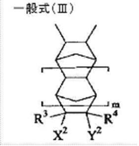

このノルボルネン系付加(共)重合体としては、市販品を用いることもできる。具体的には、三井化学(株)よりアペルの商品名で発売されており、ガラス転移温度(Tg)の異なる例えばAPL8008T(Tg70℃)、APL6013T(Tg125℃)あるいはAPL6015T(Tg145℃)などのグレードがある。ポリプラスチック(株)よりTOPAS8007、同6013、同6015などのペレットが発売されている。更に、Ferrania社よりAppear3000が発売されている。
このノルボルネン系樹脂は、市販品を用いることもでき、具体的にはJSR(株)からアートン(Arton)GあるいはアートンFという商品名で発売されており、また日本ゼオン(株)からゼオノア(Zeonor)ZF14、ZF16、ゼオネックス(Zeonex)250あるいはゼオネックス280という商品名で市販されており、これらを使用することができる。
本発明の光学積層体が有するシクロオレフィン系ポリマーフィルムは、位相差層が任意の液晶層を有している場合、液晶層と隣接する側の表面における水接触角が5°~65°となるよう表面処理されていることが好ましい。また、ポリマーフィルムの水接触角は、5°~55°であることがより好ましく、5°~50°であることが特に好ましい。
本発明において、水接触角は、下記の方法で測定された値をいう。
水接触角は、JIS R 3257:1999の静滴法に基づいて測定を行う。
また、測定には、株式会社ニック製LSE-ME1(ソフトウェア2win mini)を用いる。具体的には、純水を用いて室温20℃で、水平を保ったポリマーフィルム表面上に液滴2μLを滴下し、滴下後20秒の時点での接触角を測定する。
位相差層が有するシクロオレフィン系ポリマーフィルムの光学特性は、本発明の光学積層体を画像表示装置に使用した際に表示性能が向上する理由から、下記式(1)および下記式(2)を満たしていることが好ましく、下記式(1-1)および下記式(2-1)を満たしていることがより好ましく、下記式(1-2)および下記式(2-2)を満たしていることが更に好ましい。
なお、本発明の光学積層体が有する位相差層トータルでの光学特性は、上述した条件IIIにも示す通り、下記式(1)および(2)を満たしている必要があり、下記式(1-3)および下記式(2-3)を満たしていることが好ましく、下記式(1-4)および下記式(2-4)を満たしていることがより好ましい。
式(1) 0nm≦Re(550)≦350nm
式(2) -200nm≦Rth(550)≦200nm
式(2-1) 0nm≦Rth(550)≦200nm
式(1-2) 80nm≦Re(550)≦150nm
式(2-2) 40nm≦Rth(550)≦150nm
式(2-3) -100nm≦Rth(550)≦100nm
式(1-4) 80nm≦Re(550)≦160nm
式(2-4) -80nm≦Rth(550)≦20nm
位相差層が有するシクロオレフィン系ポリマーフィルムは、延伸により各種特性を調整することができる。詳しくは、シクロオレフィン系ポリマーフィルムを、縦方向(搬送方向)、横方向(幅方向)に延伸(一軸または二軸延伸)することによって、面内レターデーション(Re)、厚み方向のレターデーション(Rth)および任意の膜厚を発現させることができる。また、延伸方法は上記方法だけでなく、特許文献WO10/082620に開示されている熱収縮フィルムを貼合した状態で熱処理しながら面内だけでなく厚さ方向に延伸する方式でも実現可能である。以下、一般的な縦延伸および、横延伸について詳細を記載する。
(a) 横延伸
(b) 縦延伸
(c) 横延伸→緩和処理
(d) 縦延伸→緩和処理
(e) 縦延伸→横延伸
(f) 縦延伸→横延伸→緩和処理
(g) 縦延伸→緩和処理→横延伸→緩和処理
(h) 横延伸→縦延伸→緩和処理
(i) 横延伸→緩和処理→縦延伸→緩和処理
(j) 縦延伸→横延伸→縦延伸
(k) 縦延伸→横延伸→縦延伸→緩和処理
これらの中で特に重要となるのが、(a)の横延伸工程、(b)の縦延伸工程である。
シクロオレフィン系ポリマーフィルムを縦方向に延伸する場合には、例えば、複数本の予熱ローラでシクロオレフィン系ポリマーフィルムを予熱した後に、一対の延伸ローラに周速差をつけることで縦方向に延伸加工することができる。
シクロオレフィン系ポリマーフィルムを横延伸する場合には、例えばテンターを用いることで、横方向に延伸加工することができる。即ちシクロオレフィン系ポリマーフィルムの幅方向の両端部をクリップで把持し、横方向に拡幅することで延伸する。この時、テンター内に所望の温度の風を送ることで延伸温度を制御できる。
本明細書中、「延伸温度」(以下、「横延伸温度」ともいう。)は、シクロオレフィン系ポリマーフィルム膜面温度によって特定する。
延伸温度が、Tg-40℃~Tg+40℃となるように制御して行うことが好ましい。すなわち、横延伸工程の横延伸温度はTg-40℃~Tg+40℃が好ましく、より好ましくはTg-20℃~Tg+20℃、さらに好ましくはTg-10℃~Tg+10℃である。ここで、横延伸工程における横延伸温度とは、延伸開始点から延伸終了点までの間の平均温度を意味する。
シクロオレフィン系ポリマーフィルムを同時2軸延伸する場合には、通常の横延伸方法と同様、横方向にクリップを拡幅し、それと同時に縦方向に延伸、収縮することで、縦方向と横方向に同時に延伸加工することができる。具体的には、実開昭55-93520号、特開昭63-247021号、特開平6-210726号、特開平6-278204号、特開2000-334832号、特開2004-106434号、特開2004-195712号、特開2006-142595号、特開2007-210306号、特開2005-22087号、特表2006-517608号、特開2007-210306号各公報に記載されていて、いずれの公報に記載の方法も参照することができる。
高速延伸処理を行ってもよく、好ましくは20m/分以上、より好ましくは25m/分以上、さらに好ましくは30m/分以上で延伸処理することができる。
シクロオレフィン系ポリマーフィルムは、巻き取り時のブロッキング防止や、搬送安定化の観点から、塗布する面とは逆側にプロテクトフィルムを設けておくことができる。また、塗布後に塗布面側に設けることもできる。プロテクトフィルムは、たとえば偏光板加工の際、必要がなくなった段階で剥離される。プロテクトフィルムの材質としては、ハンドリングが容易である、ポリエチレン系樹脂、ポリプロピレン系樹脂、ポリスチレン系樹脂、ポリエチレンテレフタレート系樹脂などを好ましく用いることができ、これらの1種または2種以上を単層または多層状に成形したフィルムをプロテクトフィルムとして用いることができる。中でも単独で偏光フィルムに対して粘着性を有する自己粘着性のプロテクトフィルムは、プロテクトフィルム表面の粘着剤層を保護する必要性が無いことから簡便であり、より好適に使用できる。自己粘着性樹脂フィルムの市販品としては、たとえば、ポリエチレン樹脂からなるトレテック(東レ(株)製)などを挙げることができる。
なお、シクロオレフィン系ポリマーフィルムが、プロテクトフィルムを有する場合、上述した条件IIIを満たす対象(位相差層トータル)は、プロテクトフィルムを含まないものとする。
位相差層が有する任意の液晶層は、上述したシクロオレフィン系ポリマーフィルムに隣接して設けられる任意の層であり、後述する液晶性化合物を含有する液晶組成物を用いて形成される液晶層であることが好ましい。また、液晶組成物において、後述する式(I)で表される化合物は、液晶性化合物の質量に対して0.5~7.0質量%含有していることが好ましい。
なお、本明細書における液晶層の説明は、中間層として捉える液晶層、すなわち、シクロオレフィン系ポリマーフィルムの粘着剤層側に存在している液晶層にも適用されるものである。
液晶層の光学特性は、本発明の光学積層体を画像表示装置に使用した際に表示性能が向上する理由から、棒状液晶性化合物の場合は、下記式(4)および下記式(5)を満たし、ディスコティック液晶性化合物の場合は、下記式(6)および下記式(7)を満たすことが好ましい。
式(4) 0nm≦Re2(550)≦10nm
式(5) -360nm≦Rth2(550)≦-50nm
式(6) 10nm≦Re2(550)≦220nm
式(7) -110nm≦Rth2(550)≦-5nm
式(5-1) -270nm≦Rth2(550)≦-50nm
式(6-1) 20nm≦Re2(550)≦200nm
式(7-1) -100nm≦Rth2(550)≦-10nm
式(5-2) -180nm≦Rth2(550)≦-100nm
式(6-2) 60nm≦Re2(550)≦160nm
式(7-2) -80nm≦Rth2(550)≦-30nm
液晶層を形成する液晶組成物は、液晶性化合物を含有する。
液晶性化合物は、棒状液晶性化合物またはディスコティック液晶性化合物であることが好ましく、本発明の光学積層体を画像表示装置に使用した際に表示性能が向上する理由から、棒状液晶性化合物であることがより好ましい。
なお、本発明の光学積層体が有する位相差層トータルでの光学特性は、上述した条件IIIにも示す通り、下記式(1)および(2)を満たしている必要があり、下記式(1-3)および下記式(2-3)を満たしていることが好ましく、下記式(1-4)および下記式(2-4)を満たしていることがより好ましい。
式(1) 0nm≦Re(550)≦350nm
式(2) -200nm≦Rth(550)≦200nm
式(2-3) -100nm≦Rth(550)≦100nm
式(1-4) 80nm≦Re(550)≦160nm
式(2-4) -80nm≦Rth(550)≦20nm
液晶層を形成する液晶組成物は、下記式(I)で表される化合物を含有することが好ましい。
式(I) (Z)n-L100-(Q)m
ここで、式(I)中、Zは、重合性基を有する置換基を表し、nは、0~4の整数を表し、nが2~4の整数である場合、2以上のZは、それぞれ同一であっても異なっていてもよい。
また、Qは、少なくとも1つのホウ素原子を含有する置換基を表し、mは、1または2を表し、mが2の場合、2つのQは、それぞれ同一であっても異なっていてもよい。
また、L100は、n+m価の連結基を表す。ただし、nが0を表し、かつ、mが1を表す場合は、L100は、水素原子、置換もしくは無置換のアルキル基、置換もしくは無置換のアルケニル基、置換もしくは無置換のアルキニル基、置換もしくは無置換のアリール基、または、置換もしくは無置換のヘテロアリール基を表す。
これらのうち、(メタ)アクリレート基、スチリル基、オキシラニル基もしくはオキセタン基を含む置換基が好ましく、(メタ)アクリレート基またはスチリル基を含む置換基がより好ましい。

また、上記一般式(V)中、L1は、単結合、または、-O-、-CO-、-NH-、-CO-NH-、-COO-、-O-COO-、アルキレン基、アリーレン基、ヘテロ環基、および、それらの組み合わせからなる群から選ばれる二価の連結基であり、単結合、-CO-NH-または-COO-が好ましく、単結合または-CO-NH-が特に好ましい。
また、mは、1または2を表し、1を表すことが好ましい。
また、L100としては、例えば、二価の連結基として、単結合、または、-O-、-CO-、-NH-、-CO-NH-、-COO-、-O-COO-、アルキレン基、アリーレン基、ヘテロアリール基、および、それらの組み合わせから選ばれる二価の連結基が挙げられる。
これらのうち、置換もしくは無置換のアリーレン基がより好ましい。
また、L100が表すアルキル基、アルケニル基、アルキニル基、アリール基およびヘテロアリール基については、下記一般式(VI)中のR1およびR2と同義であり、好ましい範囲も同様である。
また、これらの基が有する置換基としては、例えば、特開2013-054201号公報の[0046]段落に記載された置換基などが挙げられる。
例えば、ポリマーフィルムが、表面処理等により表面にヒドロキシル基またはカルボキシル基を有する場合は、ポリマーフィルムのヒドロキシル基またはカルボキシル基と結合できる基が好ましい。なお、「ポリマーフィルムに吸着して結合することができる基」とは、ポリマーフィルムを構成している材料が有する構造と相互作用して、ポリマーフィルムに化学吸着可能な基を意味する。

アルキル基の具体例としては、メチル基、エチル基、プロピル基、ブチル基、ペンチル基、ヘキシル基、ヘプチル基、オクチル基、ノニル基、デシル基、ウンデシル基、ドデシル基、トリデシル基、ヘキサデシル基、オクタデシル基、エイコシル基、イソプロピル基、イソブチル基、sec-ブチル基、tert-ブチル基、イソペンチル基、ネオペンチル基、1-メチルブチル基、イソヘキシル基、2-メチルヘキシル基、シクロペンチル基、シクロヘキシル基、1-アダマンチル基、2-ノルボルニル基等の直鎖状、分枝状、または環状のアルキル基が挙げられる。
アルケニル基の具体例としては、ビニル基、1-プロペニル基、1-ブテニル基、1-メチル-1-プロペニル基、1-シクロペンテニル基、1-シクロヘキセニル基等の直鎖状、分枝状、または環状のアルケニル基が挙げられる。
アルキニル基の具体例としては、エチニル基、1-プロピニル基、1-ブチニル基、1-オクチニル基等が挙げられる。
アリール基の具体例としては、1個から4個のベンゼン環が縮合環を形成したもの、ベンゼン環と不飽和五員環とが縮合環を形成したものを挙げることができ、具体例としてはフェニル基、ナフチル基、アントリル基、フェナントリル基、インデニル基、アセナブテニル基、フルオレニル基、ピレニル基等が挙げられる。
窒素原子、酸素原子および硫黄原子からなる群から選ばれるヘテロ原子を1個以上含む複素芳香環の具体例としては、ピロール、フラン、チオフェン、ピラゾール、イミダゾール、トリアゾール、オキサゾール、イソオキサゾール、オキサジアゾール、チアゾール、チアジアゾール、インドール、カルバゾール、ベンゾフラン、ジベンゾフラン、チアナフテン、ジベンゾチオフェン、インダゾールベンズイミダゾール、アントラニル、ベンズイソオキサゾール、ベンズオキサゾール、ベンゾチアゾール、プリン、ピリジン、ピリダジン、ピリミジン、ピラジン、トリアジン、キノリン、アクリジン、イソキノリン、フタラジン、キナゾリン、キノキザリン、ナフチリジン、フェナントロリン、プテリジン等が挙げられる。
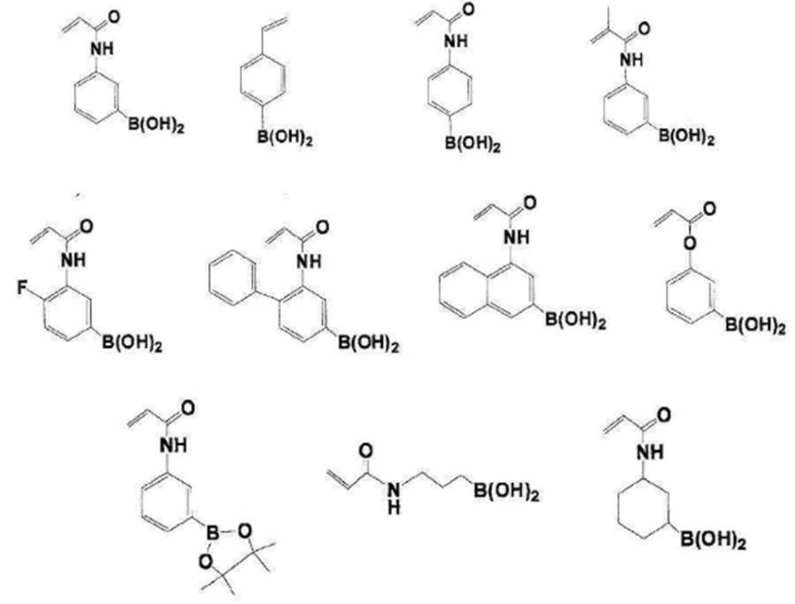
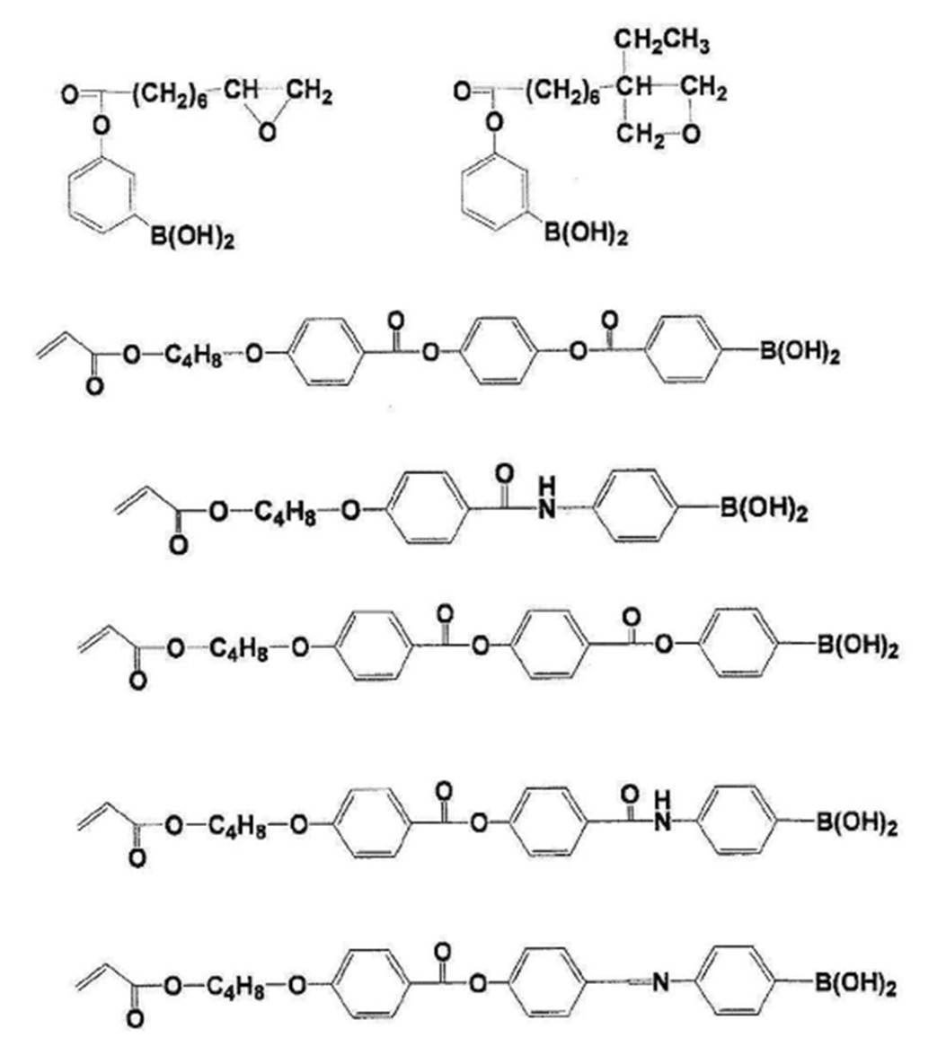
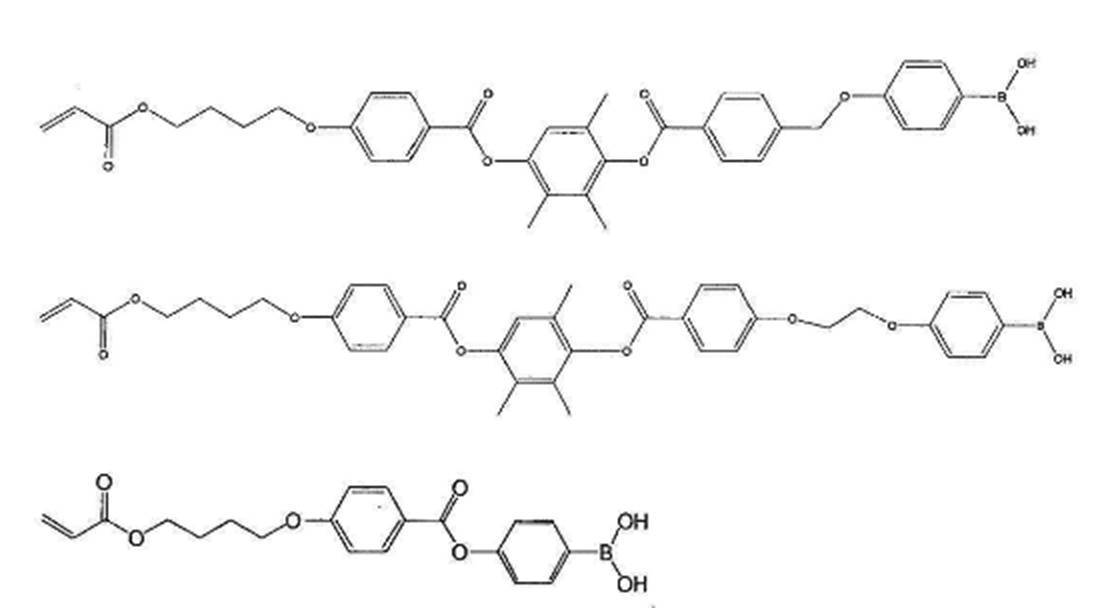
上記式(I)で表される化合物の配合量を0.5質量%以上とすることで密着性を向上でき、7質量%以下とすることで配向性を向上できる。なお、液晶性化合物が複数種含まれている時は、その合計に対しての割合である。
液晶層または液晶層を形成する液晶組成物には、本発明の趣旨を逸脱しない範囲内において、他の添加剤を配合してもよい。
他の添加剤としては、例えば、垂直配向剤が挙げられる。垂直配向剤としては、ピリジニウム化合物やオニウム化合物を使用することが好ましく、これら化合物を含有させることで、液晶性化合物のポリマーフィルム界面における垂直配向を促進する垂直配向剤として作用するとともに、液晶性化合物の配向状態を固定した液晶層とポリマーフィルムとの界面の密着性改善にも寄与する。ピリジニウム化合物については、例えば、特開2007-093864号公報の[0030]~[0052]、オニウム化合物については、例えば、特開2012-208397号公報の[0027]~[0058]に記載があり、これらの内容は本明細書に取り込まれる。
市販品としてはIRGACURE907、184、819、TPO、OXE01、OXE02、127、2959(BASF社製)等が挙げられ、重合開始剤を2種以上併用しても良い。また、ベンゾフェノン類やチオキサントン類等の各種増感剤や、各種連鎖移動剤を組み合わせて用いる事もできる。連鎖移動剤としては、チオール類が挙げられ、市販品ではカレンズMT(R)PE1、BD1、NR1(昭和電工製)等が挙げられる。
また、液晶組成物は、非液晶性の重合性モノマーを含有していてもよい。重合性モノマーとしては、ビニル基、ビニルオキシ基、アクリロイル基またはメタクリロイル基を有する化合物が好ましい。具体的には、重合性の反応性官能基数が2以上の多官能モノマー、例えば、多価アルコールと(メタ)アクリル酸とのエステル[例えばエチレングリコールジ(メタ)アクリレート、ブタンジオールジ(メタ)アクリレート、ヘキサンジオールジ(メタ)アクリレート、1,4-シクロヘキサンジアクリレート、ペンタエリスリトールテトラ(メタ)アクリレート]、ペンタエリスリトールトリ(メタ)アクリレート、トリメチロールプロパントリ(メタ)アクリレート、トリメチロールエタントリ(メタ)アクリレート、ジペンタエリスリトールテトラ(メタ)アクリレート、ジペンタエリスリトールペンタ(メタ)アクリレート、ジペンタエリスリトールヘキサ(メタ)アクリレート、ペンタエリスリトールヘキサ(メタ)アクリレート、1,2,3-シクロヘキサンテトラメタクリレート、ポリウレタンポリアクリレート、ポリエステルポリアクリレート]、上記のエチレンオキサイド変性体、ビニルベンゼン及びその誘導体(例えば1,4-ジビニルベンゼン、4-ビニル安息香酸-2-アクリロイルエチルエステル、1,4-ジビニルシクロヘキサノン)、ビニルスルホン(例えばジビニルスルホン)、アクリルアミド(例えばメチレンビスアクリルアミド)及びメタクリルアミドが挙げられる。上記モノマーは2種以上併用してもよい。
任意の液晶層を有する位相差層の製造方法(以下、単に「本製造方法」とも略す。)は、シクロオレフィン系ポリマーフィルムの表面に対して、水接触角が5°~65°となるように表面処理を施す表面処理工程と、表面処理を施した表面に対して、液晶性化合物と溶剤とを含む液晶組成物を接触させた後、液晶層を形成する液晶層形成工程とを有することが好ましい。
本製造方法が有する表面処理工程は、シクロオレフィン系ポリマーフィルム表面に対して、水接触角が5°~65°となるように表面処理する工程である。水接触角の測定方法については前述の通りである。
コロナ処理としては、例えば、特公昭39-12838号、特開昭47-19824号、特開昭48-28067号、特開昭52-42114号の各公報に記載等の処理方法によって行うことができる。コロナ処理装置は、Pillar社製ソリッドステートコロナ処理機、LEPEL型表面処理機、VETAPHON型処理機等を用いることができる。処理は空気中での常圧にて行うことができる。電極と誘電体ロールのギャップ透明ランスは0.1mm~10mm、より好ましくは1.0mm~2.0mmである。放電は、放電帯域に設けられた誘電サポートローラーの上方で処理し、処理量は、10W・min/m2~1000W・min/m2、好ましくは20W・min/m2~500W・min/m2、より好ましくは30W・min/m2~250W・min/m2である。
本製造方法が有する液晶層形成工程は、表面処理を施した表面に対して、液晶性化合物と溶剤とを含む液晶組成物を接触させた後、液晶層を形成する工程である。
液晶組成物を接触させる方法は特に限定はなく、塗布等、各種公知の方法を用いることができる。
本発明の光学積層体が有する偏光子は、特に限定はなく、自然光を特定の直線偏光に変換する機能を有するいわゆる直線偏光子であればよい。偏光子としては、特に限定されないが、吸収型偏光子を利用することができる。
偏光子と両面の偏光板保護フィルムの間の接着剤層は、その厚さを0.01~30μm程度とすることが好ましく、より好ましくは0.01~10μm、さらに好ましくは0.05~5μmである。接着剤層の厚さがこの範囲にあれば、積層される位相差フィルムと偏光子との間に浮きや剥がれを生じず、実用上問題のない接着力が得られる。
ラジカル重合性化合物としては、(メタ)アクリロイル基やビニル基等の不飽和二重結合を有するラジカル重合性化合物であれば特に限定されず、単官能ラジカル重合性化合物、分子内に2個以上の重合性基を有する多官能ラジカル重合性化合物、水酸基を有する(メタ)アクリレート、アクリルアミド、アクリロイルモルフォリン等が挙げられ、これらの化合物を単独で用いても、組み合わせて用いても良い。例えば、特開2015-11094号公報に詳細に説明されている化合物を用いることができる。また、ラジカル重合性化合物とカチオン重合性化合物を組み合わせて用いることもできる。
本発明の光学積層体は、上述した通り、偏光子の少なくとも一方の側に保護層を有する。
ここで、保護層の材料としては特に限定されず、例えばセルロースアシレートフィルム(例えば、セルローストリアセテートフィルム、セルロースジアセテートフィルム、セルロースアセテートブチレートフィルム、セルロースアセテートプロピオネートフィルム)、ポリメチルメタクリレート等のポリアクリル系樹脂フィルム、ポリエチレン、ポリプロピレン等のポリオレフィン、ポリエチレンテレフタレートやポリエチレンナフタレート等のポリエステル系樹脂フィルム、ポリエーテルスルホンフィルム、ポリウレタン系樹脂フィルム、ポリエステルフィルム、ポリカーボネートフィルム、ポリスルホンフィルム、ポリエーテルフィルム、ポリメチルペンテンフィルム、ポリエーテルケトンフィルム、(メタ)アクリルニトリルフィルム、ポリオレフィン、脂環式構造を有するポリマー(ノルボルネン系樹脂(アートン:商品名、JSR社製、非晶質ポリオレフィン(ゼオネックス:商品名、日本ゼオン社製))、などが挙げられる。
式(8) 0nm≦Re3(550)≦10nm
式(9) -40nm≦Rth3(550)≦40nm
本発明の光学積層体は、粘着剤層を有する。
粘着剤層に含まれる粘着剤としては、例えば、ゴム系粘着剤、アクリル系粘着剤、シリコーン系粘着剤、ウレタン系粘着剤、ビニルアルキルエーテル系粘着剤、ポリビニルアルコール系粘着剤、ポリビニルピロリドン系粘着剤、ポリアクリルアミド系粘着剤、セルロース系粘着剤等が挙げられる。
これらのうち、透明性、耐候性、耐熱性などの観点から、アクリル系粘着剤(感圧粘着剤)であるのが好ましい。
アクリル系粘着剤としては、(メタ)アクリル系ポリマーを用い、通常、モノマー単位として、アルキル(メタ)アクリレートを主成分として含有する。
(メタ)アクリル系ポリマーの主骨格を構成する、アルキル(メタ)アクリレートとしては、直鎖状または分岐鎖状のアルキル基の炭素数1~18のものを例示できる。これらは単独であるいは組み合わせて使用することが可能である。これらアルキル基の平均炭素数は3~9であるのが好ましい。また、フェノキシエチル(メタ)アクリレート、ベンジル(メタ)アクリレートのような芳香族環を含有するアルキル(メタ)アクリレートを用いることができる。芳香族環を含有するアルキル(メタ)アクリレートは、これを重合したポリマーを上記例示の(メタ)アクリル系ポリマーに混合して用いてもよく、上記アルキル(メタ)アクリレートと共重合して用いてもよい。透明性の観点から、共重合が好ましい。
粘着剤の詳細については、例えば、特開2018-60014号公報の[0071]-[0084]に記載されている。当該公報の記載は、本明細書に参考として援用される。
粘着剤の溶液は、例えば、トルエンや酢酸エチル等の溶剤に、粘着剤を溶解または分散させた10~40質量%程度の溶液として調製される。
塗布法は、リバースコーティング、グラビアコーティング等のロールコーティング法、スピンコーティング法、スクリーンコーティング法、ファウンテンコーティング法、ディッピング法、スプレー法などを採用できる。
ただし、シクロオレフィン系ポリマーのケミカルクラック抑制の観点からは、上記溶剤は残留しないように乾燥させることが好ましい。
また、粘着剤層の貯蔵弾性率は、耐久性がより良好となる理由から、0.18Mpa以上であることが好ましく、0.45Mpa以上であることがより好ましく、2.2Mpa以上であることが更に好ましい。また、剥離性の観点から、粘着剤層の貯蔵弾性率は、5Mpa以下であることが好ましい。
ここで、粘着剤層の貯蔵弾性率は、粘着剤を積層して、以下の方法で引張試験機にて測定した値をいう。
測定は、複数枚の粘着テープを重ねて貼合し、60℃×0.5MPa×30分間のオートクレーブを実施し、厚み1mmの動的粘弾性試験用試料を作製する。
この試料を引張試験機(せん断型レオメーター(AntonPaar社;装置名 MCR301)を用い、線形領域内、周波数1Hzの条件で動的粘弾性試験を行う。
次いで、貯蔵弾性率の測定は、-40℃~+150℃の温度範囲で、昇温速度3℃/minの条件により、30℃における値を読み取る。
また、本発明の光学積層体における粘着剤層を介してガラス基板に接着した状態で、115℃、100時間の耐久試験を行った際に、耐久試験後の粘着剤層のHS-GCMSによる測定にて、有機低分子成分(分子量32~200)が500ppm以下であると、耐久性が更に良好となる。
保温:200℃、保温時間:20min、注入時間:0.5min
カラム:DB-624UI(30m,0.25mm,1.4um)、
温度:35℃(1min),10℃/min→250℃(15min)
流量:1.5mL/min、線速度:44.0cm/sec、Split:5:1
本発明の光学積層体は、上述した条件Iを満たす場合、上述した位相差層と粘着剤層との間に、中間層を有する。
中間層としては、上述した位相差層と直接接する、有機中間層または無機中間層であることが好ましい。
また、中間層としては、上述した位相差層と粘着剤層との間に、接着剤または粘着剤を介して設けられる有機中間層であることが好ましく、ポリマーフィルムであることがより好ましい。
本発明においては、中間層は、透明であることが好ましい。なお、本明細書において、「透明」とは、可視光の透過率が60%以上であることを示し、本発明では、透過率が80%以上であることが好ましく、90%以上の透過率がより好ましい。
上述した位相差層と直接接する有機中間層(以下、「直接積層有機系中間層」とも略す。)としては、粘着剤層の有機低分子成分(揮発成分)を遮断または、吸収し、位相差層に到達しないように働けば、特に限定はなく、各種公知のものを使用できる。
直接積層有機系中間層としては、例えば、多官能モノマーを含む組成物を硬化させた層、官能基を持ったポリマーを含む組成物を硬化させた層などが挙げられる。
また、直接積層有機系中間層の他の例としては、それ自体は重合反応性のないポリマーのみから構成されるような単に乾燥固化するポリマー(以下、「ポリマーバインダー」ともいう。)で構成された層が挙げられる。このようなポリマーバインダーとしては、例えば、エポキシポリマー、ジアリルフタレートポリマー、シリコーンポリマー、フェノールポリマー、不飽和ポリエステルポリマー、ポリイミドポリマー、ポリウレタンポリマー、メラミンポリマー、ユリアポリマー、アイオノマーポリマー、エチレンエチルアクリレートポリマー、アクリロニトリルアクリレートスチレン共重合ポリマー、アクリロニトリルスチレンポリマー、アクリロニトリル塩化ポリエチレンスチレン共重合ポリマー、エチレン酢ビポリマー、エチレンビニルアルコール共重合ポリマー、アクリロニトリルブタジエンスチレン共重合ポリマー、塩化ビニルポリマー、塩素化ポリエチレンポリマー、ポリ塩化ビニリデンポリマー、酢酸セルロースポリマー、フッ素ポリマー、ポリオキシメチレンポリマー、ポリアミドポリマー、ポリアリレートポリマー、熱可塑性ポリウレタンエラストマー、ポリエーテルエーテルケトンポリマー、ポリエーテルスルホンポリマー、ポリエチレン、ポリプロピレン、ポリカーボネートポリマー、ポリスチレン、ポリスチレンマレイン酸共重合ポリマー、ポリスチレンアクリル酸共重合ポリマー、ポリフェニレンエーテルポリマー、ポリフェニレンサルファイドポリマー、ポリブタジエンポリマー、ポリブチレンテレフタレートポリマー、アクリルポリマー、メタクリルポリマー、メチルペンテンポリマー、ポリ乳酸、ポリブチレンサクシネートポリマー、ブチラールポリマー、ホルマールポリマー、ポリビニルアルコール、ポリビニルピロリドン、エチルセルロース、カルボキシメチルセルロース、ゼラチン、および、これらの共重合ポリマーが挙げられる。
このような直接積層有機系中間層の機能は特に限定されず、例えば、応力緩和層、保護層、配向層、平坦化層、屈折率調整層などの機能を有する層であってもよい。
上述した位相差層と直接接する無機中間層(以下、「直接積層無機系中間層」とも略す。)は、粘着剤層の有機低分子成分(揮発成分)を遮断し、位相差層に到達しないように働けば、特に限定はなく、酸素遮断層など各種公知のものを使用できる。
金属化合物薄層の形成方法は、目的の薄層を形成できる方法であればいかなる方法でも用いることができる。例えば、スパッタリング法、真空蒸着法、イオンプレーティング法、および、プラズマCVD(Chemical Vapor Deposition)法などが適しており、具体的には特許第3400324号、特開2002-322561号、特開2002-361774号各公報記載の形成方法を採用することができる。
上述した位相差層と粘着剤層との間に、接着剤または粘着剤を介して設けられる有機中間層は特に限定されず、通常用いるポリマーフィルム(例えば、偏光子の保護フィルムなど)を用いることができる。
ポリマーフィルムを構成するポリマーとしては、具体的には、例えば、セルロース系ポリマー;ポリメチルメタクリレート、ラクトン環含有重合体等のアクリル酸エステル重合体を有するアクリル系ポリマー;熱可塑性ノルボルネン系ポリマー;ポリカーボネート系ポリマー;ポリエチレンテレフタレート、ポリエチレンナフタレート等のポリエステル系ポリマー;ポリスチレン、アクリロニトリル・スチレン共重合体(ASポリマー)等のスチレン系ポリマー;ポリエチレン、ポリプロピレン、エチレン・プロピレン共重合体等のポリオレフィン系ポリマー;塩化ビニル系ポリマー;ナイロン、芳香族ポリアミド等のアミド系ポリマー;イミド系ポリマー;スルホン系ポリマー;ポリエーテルスルホン系ポリマー;ポリエーテルエーテルケトン系ポリマー;ポリフェニレンスルフィド系ポリマー;塩化ビニリデン系ポリマー;ビニルアルコール系ポリマー;ビニルブチラール系ポリマー;アリレート系ポリマー;ポリオキシメチレン系ポリマー;エポキシ系ポリマー;またはこれらのポリマーを混合したポリマーが挙げられる。
アクリル系ポリマーとしては、ポリメチルメタクリレートや、特開2009-98605号公報の段落[0017]~[0107]に記載されるラクトン環含有重合体等が挙げられる。
式(1) 0nm≦Re1(550)≦350nm
式(2) -200nm≦Rth1(550)≦200nm
式(1-1) 60nm≦Re1(550)≦300nm
式(2-1) -100nm≦Rth1(550)≦100nm
式(1-2) 80nm≦Re1(550)≦160nm
式(2-2) -80nm≦Rth1(550)≦20nm
本発明の画像表示装置は、上述した本発明の光学積層体を有する。
本発明の画像表示装置に用いられる表示素子は特に限定されず、例えば、液晶セル、有機エレクトロルミネッセンス(以下、「EL」と略す。)表示パネル、および、プラズマディスプレイパネル等が挙げられる。
これらのうち、液晶セルまたは有機EL表示パネルであるのが好ましく、有機EL表示パネルであるのがより好ましい。すなわち、本発明の画像表示装置としては、表示素子として液晶セルを用いた液晶表示装置、表示素子として有機EL表示パネルを用いた有機EL表示装置であるのが好ましく、有機EL表示装置であるのがより好ましい。
本発明の画像表示装置の一例である液晶表示装置としては、上述した本発明の光学積層体(ただし、λ/4板を含まない)と、液晶セルと、を有する液晶表示装置である。
なお、本発明においては、液晶セルの両側に設けられる光学積層体のうち、フロント側(視認側)の偏光素子として本発明の光学積層体を用いるのが好ましく、フロント側およびリア側の偏光素子として本発明の光学積層体を用いるのがより好ましい。
以下に、液晶表示装置を構成する液晶セルについて詳述する。
液晶表示装置に利用される液晶セルは、VA(Vertical Alignment)モード、OCB(Optically Compensated Bend)モード、IPS(In-Plane-Switching)モード、またはTN(Twisted Nematic)モードが用いられるが、これらに限定されるものではない。
VAモードの液晶セルでは、電圧無印加時に棒状液晶性分子が実質的に垂直に配向している。VAモードの液晶セルには、(1)棒状液晶性分子を電圧無印加時に実質的に垂直に配向させ、電圧印加時に実質的に水平に配向させる狭義のVAモードの液晶セル(特開平2-176625号公報記載)に加えて、(2)視野角拡大のため、VAモードをマルチドメイン化した(MVAモード(Multi-domain Vertical Alignment)の)液晶セル(SID97、Digest of tech.Papers(予稿集)28(1997)845記載)、(3)棒状液晶性分子を電圧無印加時に実質的に垂直配向させ、電圧印加時にねじれマルチドメイン配向させるモード(n-ASM(Axially symmetric aligned microcell)モード)の液晶セル(日本液晶討論会の予稿集58~59(1998)記載)および(4)SURVIVALモードの液晶セル(LCD(liquid crystal display)インターナショナル98で発表)が含まれる。また、PVA(Patterned Vertical Alignment)型、光配向型(Optical Alignment)、およびPSA(Polymer-Sustained Alignment)のいずれであってもよい。これらのモードの詳細については、特開2006-215326号公報、および特表2008-538819号公報に詳細な記載がある。
本発明においては、視野角性能の観点で、IPSモードが最も好ましい。
本発明の画像表示装置の一例である有機EL表示装置としては、例えば、視認側から、上述した本発明の光学積層体(ただし、粘着剤層およびλ/4板を含む)と、有機EL表示パネルと、をこの順で有する態様が好適に挙げられる。
有機EL表示パネルは、電極間(陰極および陽極間)に有機発光層(有機エレクトロルミネッセンス層)を挟持してなる有機EL素子を用いて構成された表示パネルである。有機EL表示パネルの構成は特に制限されず、公知の構成が採用される。
また、光学性能に優れたλ/4板として、逆波長分散性の液晶性化合物を用いることもさらに好ましい。具体的には、国際公開番号WO2017/043438に記載の一般式(II)の液晶性化合物が好ましく用いられる。逆波長分散性の液晶性化合物を用いたλ/4板の作成方法についても、WO2017/043438の実施例1~10や特開2016-91022の実施例1の記載を参考にできる。
シクロレオレフィン系ポリマーフィルム(JSR(株)製 アートン樹脂フィルム、Re=125nm、Rth=63nm、膜厚25μm)の片面に、放電量125W・min/m2でコロナ処理を施した。
次いで、コロナ処理を施した面に、以下の組成で調製した液晶層形成用組成物1を、ダイコート法で、塗布した。
次いで、組成物の溶媒の乾燥および液晶性化合物の配向熟成のために、70℃の温風で120秒加熱した後、300mJ/cm2で紫外線照射して塗布層を硬化させて光学異方性層(液晶層)を形成した。作製した位相差フィルムのReは124nm、Rthは-28nmであった。
なお、以下では、作製した位相差フィルムに含まれる液晶層を「第1の位相差層」といい、シクロレオレフィン系ポリマーフィルムを「第2の位相差層」とも略す。
Re=(nx-ny)×d
Nz=(nx-nz)/(nx-ny)
ただし、dは厚みを表す。
したがって、Nz係数が、0.90~1.10の範囲内であれば、本発明のny=nzのNz=1.0のポジティブAプレートとみなしてもよく、好ましくは、0.95~1.05である。
液晶層形成用組成物1
―――――――――――――――――――――――――――――――――
・下記液晶性化合物R1 100.0質量部
・下記配向助剤(A1) 1.5質量部
・下記式(I)で表される化合物B1 3.0質量部
・ATMMT 5.0質量部
(新中村化学工業製 ペンタエリスリトールテトラアクリレート)
・下記重合開始剤(P1) 2.0質量部
・下記重合開始剤(P2) 5.0質量部
・下記界面活性剤(S1) 0.3質量部
・下記界面活性剤(S2) 0.5質量部
・アセトン 425.6質量部
・プロピレングリコールモノメチルエーテルアセテート 48.9質量部
・メタノール 14.7質量部
―――――――――――――――――――――――――――――――――
下記液晶性化合物(RA)(RB)(RC)の83:15:2(質量比)の混合物



重合開始剤(P2):Omnnirad127(IGM Resins B.V.製)

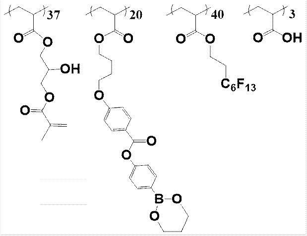
〔コア層セルロースアシレートドープ1の作製〕
下記の組成物をミキシングタンクに投入し攪拌して、各成分を溶解し、コア層セルロースアシレートドープ1を調製した。
――――――――――――――――――――――――――――――
コア層セルロースアシレートドープ1
――――――――――――――――――――――――――――――
・アセチル置換度2.88のセルロースアセテート 100質量部
・下記エステルオリゴマーA 10質量部
・下記偏光子耐久性改良剤 4質量部
・下記紫外線吸収剤 2質量部
・メチレンクロライド(第1溶媒) 430質量部
・メタノール(第2溶剤) 64質量部
――――――――――――――――――――――――――――――
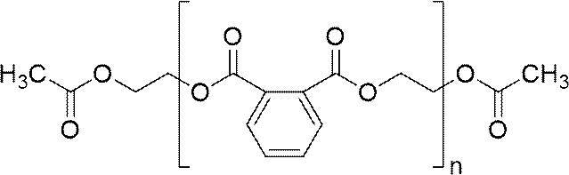

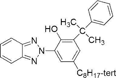
上記のコア層セルロースアシレートドープ1の90質量部に下記のマット剤溶液を10質量部加え、外層セルロースアシレートドープ1を調製した。
――――――――――――――――――――――――――――――
外層セルロースアシレートドープ1
――――――――――――――――――――――――――――――
・平均粒子サイズ20nmのシリカ粒子
(AEROSIL R972、日本アエロジル(株)製)
2質量部
・メチレンクロライド(第1溶媒) 76質量部
・メタノール(第2溶剤) 11質量部
・コア層セルロースアシレートドープ1 1質量部
――――――――――――――――――――――――――――――
上記コア層セルロースアシレートドープ1とその両側に外層セルロースアシレートドープ1とを3層同時に流延口から20℃のドラム上に流延した。溶剤含有率略20質量%の状態で剥ぎ取り、フィルムの幅方向の両端をテンタークリップで固定し、残留溶剤が3~15%の状態で、横方向に1.1倍延伸しつつ乾燥した。その後、熱処理装置のロール間を搬送することにより、さらに乾燥し、厚さ40μmのセルロースアシレートフィルム1を作製し、保護フィルム100とした。保護フィルム100の位相差を測定した結果、Re=2nm、Rth=7nmであった。
〔コア層セルロースアシレートドープ2の作製〕
下記の組成物をミキシングタンクに投入し、攪拌して、各成分を溶解し、コア層セルロースアシレートドープ2を調製した。
――――――――――――――――――――――――――――――――
コア層セルロースアシレートドープ2
――――――――――――――――――――――――――――――――
・アセチル置換度2.88のセルロースアセテート 100質量部
・下記ポリエステル 12質量部
・上記偏光子耐久性改良剤 4質量部
・メチレンクロライド(第1溶媒) 430質量部
・メタノール(第2溶剤) 64質量部
――――――――――――――――――――――――――――――――
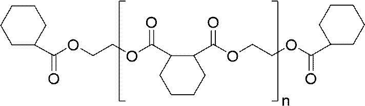
上記のコア層セルロースアシレートドープ2の90質量部に下記のマット剤溶液を10質量部加え、外層セルロースアシレートドープ2を調製した。
―――――――――――――――――――――――――――――――
マット剤溶液
―――――――――――――――――――――――――――――――
・平均粒子サイズ20nmのシリカ粒子
(AEROSIL R972、日本アエロジル(株)製)
2質量部
・メチレンクロライド(第1溶媒) 76質量部
・メタノール(第2溶剤) 11質量部
・コア層セルロースアシレートドープ 1質量部
―――――――――――――――――――――――――――――――
上記コア層セルロースアシレートドープ2と上記外層セルロースアシレートドープ2を平均孔径34μmのろ紙および平均孔径10μmの焼結金属フィルターでろ過した後、上記コア層セルロースアシレートドープ2とその両側に外層セルロースアシレートドープ2とを3層同時に流延口から20℃のドラム上に流延した(バンド流延機)。
次いで、溶剤含有率略20質量%の状態で剥ぎ取り、フィルムの幅方向の両端をテンタークリップで固定し、横方向に延伸倍率1.1倍で延伸しつつ乾燥した。
その後、熱処理装置のロール間を搬送することにより、さらに乾燥し、厚み40μmのセルロースアシレートフィルム2を作製し、低レターデーションフィルム210とした。低レターデーションフィルム210の位相差を測定した結果、Re=1nm、Rth=-5nmであった。
上記作製した保護フィルム100を、2.3mol/Lの水酸化ナトリウム水溶液に、55℃で3分間浸漬した。室温の水洗浴槽中で洗浄し、30℃で0.05mol/Lの硫酸を用いて中和した。再度、室温の水洗浴槽中で洗浄し、さらに100℃の温風で乾燥し、保護フィルム表面の鹸化処理を行った。
上記作製したけん化処理した保護フィルム100、ポリビニルアルコール系偏光子、および、上記作製した位相差フィルムを、偏光子の吸収軸と位相差フィルムの遅相軸が平行な方向になるように、位相差フィルムの液晶層(第1の位相差層)側と偏光子を接着剤を用いて貼り合わせ、上偏光板を作製した。
接着剤としては、PVA((株)クラレ製、PVA-117H)3%水溶液を用いた。
また、下側偏光板は、けん化処理した保護フィルム、ポリビニルアルコール系偏光子、および、上記作製したけん化処理した保護フィルム100を同様に貼り合わせて作製した。このとき、偏光子と位相差フィルムは、実用上十分な接着性であった。
以下の手順に従い、アクリル系ポリマーの粘着剤を調製し、粘着剤I、IIおよびIIIを得た。
粘着剤I(分子量500以下の有機低分子成分:2.6質量%)
――――――――――――――――――――――――――――――――
・主剤(SKダインSF-2147) 200g(16%固形分)
・架橋剤 80mg
・シランカップリング剤 120mg
・AS剤(1-オクチル-4-メチルピリジニウム
=ビス(トリフルオロメタンスルホニル)イミド) 670mg
――――――――――――――――――――――――――――――――
粘着剤II(分子量500以下の有機低分子成分:0.6質量%)
――――――――――――――――――――――――――――――――
・主剤(SKダインSF-2147) 200g(16%固形分)
・架橋剤 80mg
・シランカップリング剤 120mg
――――――――――――――――――――――――――――――――
粘着剤III(分子量500以下の有機低分子成分:5.5質量%)
――――――――――――――――――――――――――――――――
・主剤(SKダインSF-2147) 200g(16%固形分)
・架橋剤 80mg
・シランカップリング剤 120mg
・AS剤(1-オクチル-4-メチルピリジニウム
=ビス(トリフルオロメタンスルホニル)イミド) 1670mg
――――――――――――――――――――――――――――――――
以下の手順に従い、アクリル系ポリマーを調製した。
冷却管、窒素導入管、温度計及び撹拌装置を備えた反応容器に、2-エチルヘキシルアクリレート70質量部、アクリル酸エチル20質量部、ヒドロキシエチルメタクリレート6質量部、ベンジルアクリレート5質量部および、アクリル酸4質量部を溶液重合法により重合させて、平均分子量25万のアクリル系ポリマーの粘着剤IVを得た。
以下の手順に従い、アクリル系ポリマーを調製した。
冷却管、窒素導入管、温度計及び撹拌装置を備えた反応容器に、2-エチルヘキシルアクリレート70質量部、アクリル酸エチル20質量部、ヒドロキシエチルメタクリレート6質量部および、アクリル酸4質量部を溶液重合法により重合させて、平均分子量30万のアクリル系ポリマーの粘着剤Vを得た。
得られた上記粘着剤I、II、III、IVおよびVを用いて、以下の手順に従い、粘着剤シートを作製した。
次いで、調製した粘着剤組成物を、シリコーン系剥離剤で表面処理したPETフィルムにダイコーターを用いて塗布し、150℃で3時間乾燥させ、厚み15μmの粘着剤層を有する粘着剤シートを作製した。粘着剤層の貯蔵弾性率は0.18MPaであった。
粘着剤VIとしてOpteriaD692(厚み15μm、貯蔵弾性率2.2MPa、リンテック社製)を用いた。
また、粘着剤VIIとして、SK1478(厚み25μm、貯蔵弾性率0.45MPa、綜研化学社製)を用いた。
上記で作製した上偏光板に対して、上記粘着剤IIIを用いた粘着シートを積層させて光学積層体を作製した。
次いで、作製した光学積層体について後述する耐久性を評価した結果、下記表1に示すように、光学積層体の面内に多数のクラックが発生することが確認された。
粘着剤IIIに代えて粘着剤Iを適用する以外は、比較例1と同じ条件で光学積層体を作製した。
次いで、作製した光学積層体について後述する耐久性を評価した結果、下記表1に示すように、光学積層体の面内のクラックが比較例1の構成に対して改善することが分かった。
粘着剤Iに代えて粘着剤IIを適用する以外は、実施例1と同じ条件で光学積層体を作製した。
次いで、作製した光学積層体について後述する耐久性を評価した結果、下記表1に示すように、光学積層体の面内にクラックが発生しないことを確認した。有機低分子成分の減少が、シクロオレフィン含有位相差のクラック耐性を大幅に改善することを見出した。
粘着剤Iに代えて粘着剤IVを適用する以外は、実施例1と同じ条件で光学積層体を作製した。
次いで、作製した光学積層体について後述する耐久性を評価した結果、下記表2に示すように、光学積層体の面内にクラックが多発することが分かった。
また、HS-GCMSの解析結果より、粘着剤層(粘着剤)に含まれる分子量32~200の有機低分子成分の含有量を評価したところ、分子量32~200以下の有機低分子成分(未反応モノマが主)が1500ppm含まれており、また、耐久試験後においても有機低分子成分の含有量に変化がないことが分かり、この有機低分子成分が多い点がシクロオレフィン系ポリマー位相差のクラック発生要因と考えた。
粘着剤Iに代えて粘着剤Vを適用する以外は、実施例1と同じ条件で光学積層体を作製した。
次いで、作製した光学積層体について後述する耐久性を評価した結果、下記表2に示すように、光学積層体の面内にクラックは僅かに発生するが、大幅に改善することが分かった。この結果から、粘着剤IVと粘着剤Vの差異より、環状構造を有する(メタ)アクリル酸エステル系単量体、特にベンジルアクリレートを含まない(またはHS-GCMSで検出限界以下)こと、および、耐久試験後において有機低分子成分の含有量が減少することが、シクロオレフィンのクラック抑制に効果あることを見出した。
特に、ベンジルアクリレートなどが含まれると、耐久過程で酸化され、ベンズアルデヒドや安息香酸などの低分子をさらに生成するためにクラック耐性が悪化すると考えた。
粘着剤Iに代えて粘着剤VIを適用する以外は、実施例1と同じ条件で光学積層体を作製した。
次いで、作製した光学積層体について後述する耐久性を評価した結果、下記表2に示すように、光学積層体の面内にクラックが発生しないことが分かった。
また、粘着剤層(粘着剤IV)のHS-GCMSの解析結果より、粘着剤VIはベンジルアクリレートなどの環状構造を有する(メタ)アクリル酸エステル系単量体を含む有機低分子成分(分子量200以下)が少なく(500ppmであり)、耐久試験後において有機低分子成分の含有量が減少することがシクロオレフィンのクラック抑制に大幅に効果あることを見出した。
粘着剤Iに代えて粘着剤VIIを適用する以外は、実施例1と同じ条件で光学積層体を作製した。
次いで、作製した光学積層体について後述する耐久性を評価した結果、下記表2に示すように、光学積層体の面内にクラックが発生しないことが分かった。
また、粘着剤層(粘着剤VII)のHS-GCMSの解析結果より、粘着剤VIIは環状構造を有する(メタ)アクリル酸エステル系単量体を含む有機低分子成分(分子量200以下)が非常少なく(50ppm以下であり)、耐久試験後において有機低分子成分の含有量が検出限界以下となることが、シクロオレフィンのクラック抑制に大幅に効果あることを見出した。
粘着剤IVを適用した比較例2の構成において、第2の位相差層の粘着剤層側の表面に有機中間層としてアクリレート系ポリマー層1(厚み2μm)を直接積層させた以外は、比較例2と同じ条件で光学積層体を作製した。光学積層体の層構成を図3に示す。
以下に、アクリレート系ポリマー層1の形成方法を示す。
次いで、下記組成のアクリレート系ポリマー組成物1を、ダイコート法で、塗布した。
次いで、組成物の溶媒の乾燥のために、70℃の温風で120秒加熱した後、300mJ/cm2で紫外線照射して塗布層を硬化させてアクリレート系ポリマー層1を形成した。
アクリレート系ポリマー組成物1
―――――――――――――――――――――――――――――――――
・ATMMT 100.0質量部
・上記式(I)で表される化合物B1 3.0質量部
・重合開始剤(P2) 3.0質量部
(IGM ResinsB.V.製Omnirad127)
・上記界面活性剤(S2) 0.5質量部
・アセトン 425.6質量部
・プロピレングリコールモノメチルエーテルアセテート 48.9質量部
・メタノール 14.7質量部
―――――――――――――――――――――――――――――――――
これは、粘着剤の低分子成分のシクロオレフィン側への移動を抑制することおよび、シクロオレフィン系ポリマーの剛性をアップすることで、シクロオレフィンのクラック抑制に効果あると考えた。なお、ここでの剛性とは、機械物性的に弾性率X膜厚を指標としている。
粘着剤IVを適用した実施例6の構成において、第2の位相差層の粘着剤層側の表面に有機中間層としてアクリレート系ポリマー層2(厚み1μm)を直接積層させた以外は、実施例6と同じ条件で光学積層体を作製した。
以下に、アクリレート系ポリマー層2の形成方法を示す。
次いで、下記組成のアクリレート系ポリマー組成物2を、ダイコート法で、塗布した。
次いで、組成物の溶媒の乾燥のために、70℃の温風で120秒加熱した後、300mJ/cm2で紫外線照射して塗布層を硬化させてアクリレート系ポリマー層2を形成した。
アクリレート系ポリマー組成物2
―――――――――――――――――――――――――――――――――
・ATMMT 75.0質量部
・A600 25.0質量部
(新中村化学工業製 2官能ポリエチレングリコールアクリレート)
・上記式(I)で表される化合物B1 3.0質量部
・重合開始剤(P2) 5.0質量部
(IGM ResinsB.V.製Omnirad127)
・上記界面活性剤(S2) 0.5質量部
・アセトン 425.6質量部
・プロピレングリコールモノメチルエーテルアセテート 48.9質量部
・メタノール 14.7質量部
―――――――――――――――――――――――――――――――――
これは、粘着剤の低分子成分のシクロオレフィン側への移動を抑制することおよび、シクロオレフィン系ポリマーの剛性をアップすることで、シクロオレフィンのクラック抑制に効果あると考えた。
粘着剤IVを適用した実施例7の構成において、上記液晶層形成用組成物1を、ダイコート法の液吐出量を調整(6%減少)して塗布し、乾燥させ、紫外線照射により硬化させて第1の位相差層を形成し、また、第2の位相差層の粘着剤層側の表面に有機中間層として、下記アクリレート系ポリマー層2-2(厚み3μm)を直接積層させた以外は、実施例7と同じ条件で光学積層体を作製した。
以下に、アクリレート系ポリマー層2-2の形成方法を示す。
次いで、下記組成のアクリレート系ポリマー組成物2-2を、ダイコート法で、紫外線照射による硬化後の膜厚が3μmになるように塗布膜厚を調整して塗布した。
次いで、組成物の溶媒の乾燥のために、70℃の温風で120秒加熱した後、300mJ/cm2で紫外線照射して塗布層を硬化させてアクリレート系ポリマー層2-2を形成した。作製した位相差および中間層含めたトータルの位相差はReは124nm、Rthは-21nmであった。
アクリレート系ポリマー組成物2-2
―――――――――――――――――――――――――――――――――
・ATMMT 75.0質量部
・A600 25.0質量部
(新中村化学工業製 2官能ポリエチレングリコールアクリレート)
・上記式(I)で表される化合物B1 3.0質量部
・重合開始剤(P2) 5.0質量部
(IGM ResinsB.V.製Omnirad127)
・下記界面活性剤(S3) 0.5質量部
・アセトン 425.6質量部
・プロピレングリコールモノメチルエーテルアセテート 48.9質量部
・メタノール 14.7質量部
―――――――――――――――――――――――――――――――――
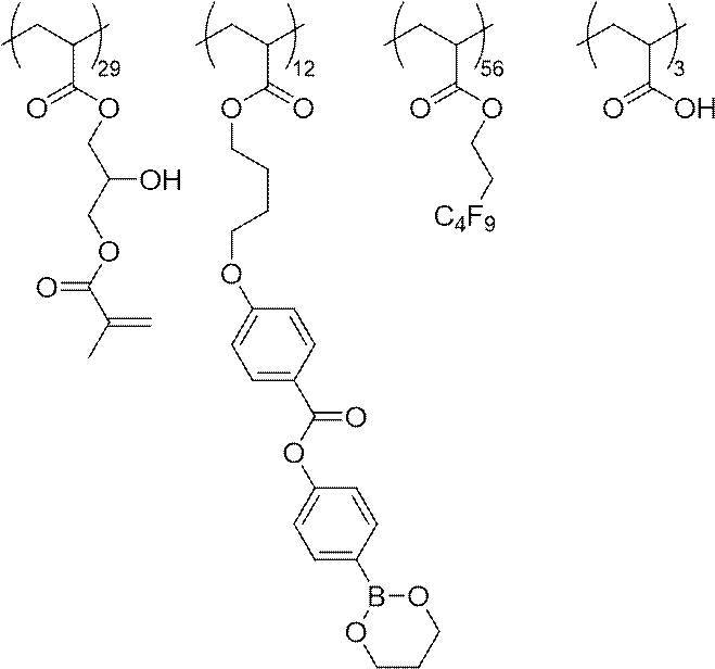
これは、粘着剤の低分子成分のシクロオレフィン側への移動を抑制することおよび、シクロオレフィン系ポリマーの剛性をアップすることで、シクロオレフィンのクラック抑制に効果あると考えた。
粘着剤IVを適用した実施例7-1の構成において、上記液晶層形成用組成物1を、ダイコート法の液吐出量を調整(6%減少)して塗布し、乾燥させ、紫外線照射により硬化させて第1の位相差層を形成し、また、第2の位相差層を、シクロレオレフィン系ポリマーフィルム(JSR(株)製 アートン樹脂フィルム、Re=135nm、Rth=68nm、膜厚24μm)に変更し、更に、第2の位相差層の粘着剤層側の表面に有機中間層として、下記アクリレート系ポリマー層2-2(厚み2μm)を直接積層させた以外は、実施例7-1と同じ条件で光学積層体を作製した。
以下に、アクリレート系ポリマー層2-2の形成方法を示す。
次いで、上記組成のアクリレート系ポリマー組成物2-2を、ダイコート法で、紫外線照射による硬化後の膜厚が2μmになるように塗布膜厚を調整して、塗布した。
次いで、組成物の溶媒の乾燥のために、70℃の温風で120秒加熱した後、300mJ/cm2で紫外線照射して塗布層を硬化させてアクリレート系ポリマー層2-2を形成した。作製した位相差および中間層含めたトータルの位相差はReは135nm、Rthは-12nmであった。
これは、粘着剤の低分子成分のシクロオレフィン側への移動を抑制することおよび、シクロオレフィン系ポリマーの剛性をアップすることで、シクロオレフィンのクラック抑制に効果あると考えた。
粘着剤IVを適用した実施例7-2の構成において、上記液晶層形成用組成物1を、ダイコート法の液吐出量を調整(25%増加)して塗布し、乾燥させ、紫外線照射により硬化させて第1の位相差層を形成し、また、第2の位相差層の粘着剤層側の表面に有機中間層として、下記アクリレート系ポリマー層2-2(厚み5μm)を直接積層させた以外は、実施例7-2と同じ条件で光学積層体を作製した。
以下に、アクリレート系ポリマー層2-2の形成方法を示す。
次いで、上記組成のアクリレート系ポリマー組成物2-2を、ダイコート法で、紫外線照射による硬化後の膜厚が5μmになるように塗布膜厚を調整して塗布した。
次いで、組成物の溶媒の乾燥のために、70℃の温風で120秒加熱した後、300mJ/cm2で紫外線照射して塗布層を硬化させてアクリレート系ポリマー層2-2を形成した。作製した位相差および中間層含めたトータルの位相差はReは135nm、Rthは-30nmであった。
これは、粘着剤の低分子成分のシクロオレフィン側への移動を抑制することおよび、シクロオレフィン系ポリマーの剛性をアップすることで、シクロオレフィンのクラック抑制に効果あると考えた。
粘着剤IVを適用した実施例6の構成において、第2の位相差層の粘着剤層側の表面に有機中間層としてアクリレート系ポリマー層3(厚み1μm)を直接積層させた以外は、実施例6と同じ条件で光学積層体を作製した。
以下に、アクリレート系ポリマー層3の形成方法を示す。
次いで、下記組成のアクリレート系ポリマー組成物3を、ダイコート法で、塗布した。
次いで、組成物の溶媒の乾燥のために、70℃の温風で120秒加熱した後、300mJ/cm2で紫外線照射して塗布層を硬化させてアクリレート系ポリマー層3を形成した。
アクリレート系ポリマー組成物3
―――――――――――――――――――――――――――――――――
・PET30 100.0質量部
(日本化薬製 ペンタエリスリトールトリアクリレート)
・上記式(I)で表される化合物B1 3.0質量部
・重合開始剤(P2) 3.0質量部
(IGM ResinsB.V.製Omnirad127)
・上記界面活性剤(S2) 0.5質量部
・アセトン 425.6質量部
・プロピレングリコールモノメチルエーテルアセテート 48.9質量部
・メタノール 14.7質量部
―――――――――――――――――――――――――――――――――
これは、粘着剤の低分子成分のシクロオレフィン側への移動を抑制することおよび、シクロオレフィン系ポリマーの剛性をアップすることで、シクロオレフィンのクラック抑制に効果あると考えた。
粘着剤IVを適用した実施例6の構成において、第2の位相差層の粘着剤層側の表面に有機中間層として液晶層形成用組成物1(0.25μm)を直接積層させた以外は、実施例6と同じ条件で光学積層体を作製した。
具体的には、シクロレオレフィン系ポリマーフィルム(JSR(株)製 アートン樹脂フィルム、Re=124nm、Rth=63nm、膜厚24μm)の液晶層(第1の位相差層)と反対側の表面に、放電量125W・min/m2でコロナ処理を施した。
次いで、液晶層形成用組成物1を、ダイコート法で、塗布した。
次いで、組成物の溶媒の乾燥のために、70℃の温風で120秒加熱した後、300mJ/cm2で紫外線照射して塗布層を硬化させて液晶層を形成した。
次いで、作製した光学積層体について後述する耐久性を評価した結果、下記表2に示すように、光学積層体の面内にクラックが比較例2より改善することを確認した。
これは、粘着剤の低分子成分のシクロオレフィン側への移動を抑制することおよび、シクロオレフィン系ポリマーの剛性をアップすることで、シクロオレフィンのクラック抑制に効果あると考えた。
有機中間層(アクリレート系ポリマー)に代えて、無機中間層としてSIO2スパッタ膜(1μm)を適用した以外は、実施例6と同じ条件で光学積層体を作製した。
次いで、作製した光学積層体について後述する耐久性を評価した結果、下記表3に示すように、光学積層体の面内にクラックが改善することを確認した。
これは、粘着剤の低分子成分のSiOxスパッタ膜が有機低分子成分の移動を抑制することおよび、スパッタ膜がシクロオレフィン系ポリマーの剛性をアップすることでクラック耐性が改善したと考えた。
第2の位相差層の粘着剤層側の表面に、上記UV接着(膜厚2μm)を用いて、低レターデーションのアクリルフィルム(40μm)を有機中間層として適用した以外は、実施例6と同じ条件で光学積層体を作製した。光学積層体の層構成を図4に示す。
次いで、作製した光学積層体について後述する耐久性を評価した結果、下記表3に示すように、光学積層体の面内にクラックが改善することを確認した。
これは、粘着剤の低分子成分の中間層のアクリルフィルムで有機低分子成分の移動が抑制されたこと、および、シクロオレフィン系ポリマーとアクリルフィルムがUV接着され剛性が高まったことで改善したと考えた。
アクリルフィルム(40μm)に代えて、上記で作製した低レターデーションフィルムを有機中間層として適用した以外は、実施例8と同じ条件で光学積層体を作製した。
次いで、作製した光学積層体について後述する耐久性を評価した結果、下記表3に示すように、光学積層体の面内にクラックが改善することを確認した。
これは、粘着剤の低分子成分の中間層のセルロースアシレートフィルムで有機低分子成分の移動が抑制されたこと、および、シクロオレフィン系ポリマーとセルロースアシレートフィルムがUV接着され剛性が高まったことで改善したと考えた。
第2の位相差層の粘着剤層側の表面に、上記層間粘着剤(5μm)を用いて、シクロオレフィンフィルム(ゼオノアフィルム40μm)を有機中間層として適用した以外は、実施例8と同じ条件で光学積層体を作製した。
次いで、作製した光学積層体について後述する耐久性を評価した結果、下記表3に示すように、光学積層体の面内にクラックが改善することを確認した。
これは、粘着剤の低分子成分の中間層のシクロオレフィンフィルムで有機低分子成分の移動が抑制より、シクロオレフィンフィルムの積層で剛性が上がることがより効果があると考えにいたった。
位相差フィルムとして、液晶層(第1の位相差層)を用いず、シクロレオレフィン系ポリマーフィルム(第2の位相差層)を単独で用いた以外は、実施例4と同じ条件で光学積層体を作製した。光学積層体の層構成を図6に示す。なお、図6中、符号21は、シクロオレフィン系ポリマーフィルム(位相差層)の遅相軸を表す。
次いで、作製した光学積層体について後述する耐久性を評価した結果、下記表3に示すように、光学積層体の面内にクラックが改善することを確認した。
第1の位相差層と第2の位相差層が逆転した構成を適用した以外は、比較例2と同じ条件で光学積層体を作製した。光学積層体の層構成を図5に示す。
次いで、作製した光学積層体について後述する耐久性を評価した結果、下記表3に示すように、光学積層体の面内にクラックが改善することを確認した。
これは、液晶層(アクリレイト重合ポリマー)が粘着剤側に配置されることで、液晶層が有機中間層を兼ね、粘着剤の有機低分子成分の移動が抑制されたことで、クラックが改善したと考えにいたった。
得られた各光学積層体について耐久性を評価した。
具体的には、光学積層体を300mm×100mm角にカットした後、粘着剤層側をガラス基板に貼り合わせた後、115℃ドライの恒温槽に100時間静置する耐久試験を行い、耐久試験後、常温常湿環境下で1週間放置後までのクラック発生を観察し、以下の評点をつけた。
A:N=2でクラック発生は見られなかった。
B:N=2のうち、いずれか一方で1~3カ所程度のクラック発生が見られた。
(実験的なエラーレベルを含む)
C:10カ所未満の2mm程度の微小なクラックが発生。
(視認し難いレベル)
D:面内で非常に多数(数十カ所以上)の5mmから10mm程度のクラックが発生。
(明確に視認できるクラックが多数発生)
結果を下記表1~表3に示す。実用上、視認性の観点で、Cは明らかな改善効果あり、実用上はAからBであることが好ましく、Aであることがより好ましい。
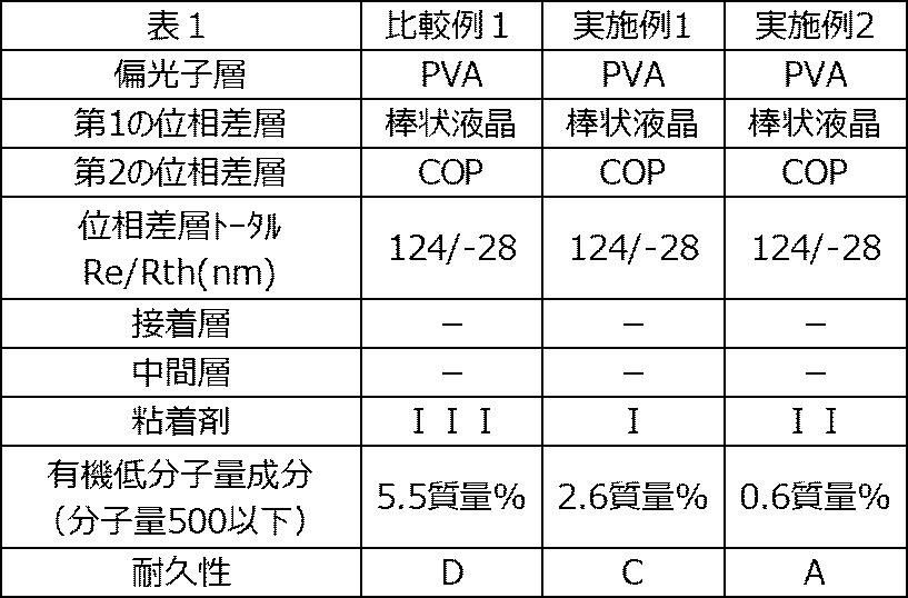
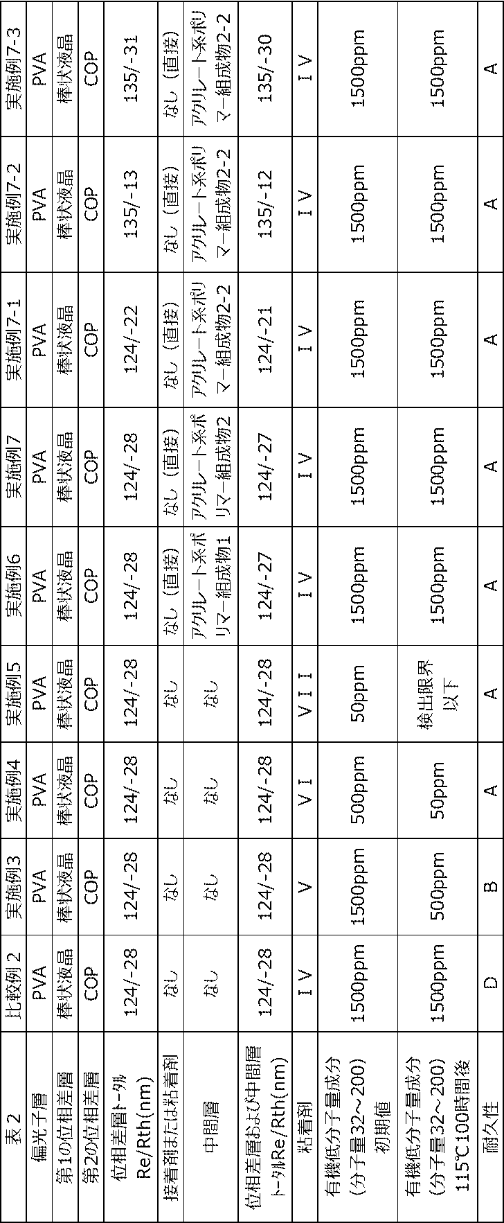

特に、実施例同士の対比から、有機低分子成分として、環状構造を有する(メタ)アクリル酸エステル系単量体を低減する必要性があること、AS剤などの低分子成分も極力低減すること、および、剛性の観点から粘着剤層の貯蔵弾性率が高い必要があることを新たに見出した。
12 第2偏光子吸収軸
21 シクロオレフィン系ポリマーフィルム(位相差層)の遅相軸
22 液晶層(第1の位相差層)の遅相軸
23 シクロオレフィン系ポリマーフィルム(第2の位相差層)の遅相軸
31 IPS液晶セルの液晶ダイレクタ方向(液晶配向方向)
100 保護フィルム
101 偏光子
200 シクロオレフィン系ポリマーフィルム(位相差層)
201 液晶層(第1の位相差層)
202 シクロオレフィン系ポリマーフィルム(第2の位相差層)
210 低レターデーションフィルム(等方性位相差フィルム)
300 粘着剤層
301 低分子低減粘着剤層
302 接着剤または粘着剤
400 IPS液晶セル
500 中間層(直接積層)
501 中間層(フィルム)
Claims (10)
- 偏光子と、シクロオレフィン系ポリマーフィルムを含む位相差層と、粘着剤層と、をこの順に有し、
前記偏光子が、少なくとも一方の側に保護層を有し、
下記条件Iおよび条件III、または、条件IIおよび条件IIIを満たす、光学積層体。
条件I:前記位相差層と前記粘着剤層との間に、中間層をさらに有する。
条件II:前記粘着剤層が分子量500以下の有機低分子成分を含有し、前記分子量500以下の有機低分子成分の含有量が2.6質量%以下である、または、前記位相差層と前記粘着剤層とが直接接し、かつ、前記粘着剤層を介してガラス基板に接着した状態で、115℃、100時間の耐久試験を行った際に、前記耐久試験後の前記粘着剤層中の分子量32~200の有機低分子成分の含有量が、前記耐久試験前の含有量と比較して50%以下である。
条件III:前記位相差層トータルでの、波長550nmでの面内レターデーションRe(550)、および、厚み方向レターデーションRth(550)が、それぞれ、下記式(1)および下記式(2)を満たす。
式(1) 0nm≦Re(550)≦350nm
式(2) -200nm≦Rth(550)≦200nm - 前記条件Iを満たし、
前記位相差層と前記中間層とが直接接し、前記中間層が有機中間層または無機中間層である、請求項1に記載の光学積層体。 - 前記条件Iを満たし、
前記中間層が、前記位相差層と前記粘着剤層との間に、0.1~50μmの膜厚を有する接着剤または粘着剤を介して設けられたポリマーフィルムである、請求項1に記載の光学積層体。 - 前記ポリマーフィルムが、シクロオレフィン系ポリマー、アクリル系ポリマー、ポリカーボネート系ポリマー、および、セルロース系ポリマーフィルムからなる群から選択される少なくとも1種を含有する、請求項3に記載の光学積層体。
- 前記条件Iを満たし、
前記位相差層および前記中間層のトータルでの、波長550nmにおける面内レターデーションRe1(550)、および、厚み方向レターデーションRth1(550)が、それぞれ、下記式(1)および下記式(2)を満たす、請求項1~4のいずれか1項に記載の光学積層体。
式(1) 0nm≦Re1(550)≦350nm
式(2) -200nm≦Rth1(550)≦200nm - 前記粘着剤層のヘッドスペース型ガスクロマト質量分析計による測定にて、分子量32~200の有機低分子成分が1000ppm以下である、請求項1~5のいずれか1項に記載の光学積層体。
- 前記粘着剤層を介してガラス基板に接着した状態で、115℃、100時間の耐久試験を行った際に、耐久試験後の前記粘着剤層のヘッドスペース型ガスクロマト質量分析計による測定にて、分子量32~200の有機低分子成分が500ppm以下である、請求項1~6のいずれか1項に記載の光学積層体。
- 前記粘着剤層の膜厚が5μm以上50μm以下であり、前記粘着剤層の貯蔵弾性率が0.18MPa以上5Mpa以下である、請求項1~7のいずれか1項に記載の光学積層体。
- 前記粘着剤層中の環状構造を有するアクリル酸エステル系またはメタクリル酸エステル系の単量体の残留量が100ppm以下である、請求項1~8のいずれか1項に記載の光学積層体。
- 請求項1~9のいずれか1項に記載の光学積層体を備える、画像表示装置。
Priority Applications (3)
| Application Number | Priority Date | Filing Date | Title |
|---|---|---|---|
| CN202280010708.8A CN116783519A (zh) | 2021-01-19 | 2022-01-19 | 光学层叠体及图像显示装置 |
| JP2022576714A JPWO2022158482A1 (ja) | 2021-01-19 | 2022-01-19 | |
| US18/349,649 US20230350118A1 (en) | 2021-01-19 | 2023-07-10 | Optical laminate and image display device |
Applications Claiming Priority (4)
| Application Number | Priority Date | Filing Date | Title |
|---|---|---|---|
| JP2021-006428 | 2021-01-19 | ||
| JP2021006428 | 2021-01-19 | ||
| JP2021112542 | 2021-07-07 | ||
| JP2021-112542 | 2021-07-07 |
Related Child Applications (1)
| Application Number | Title | Priority Date | Filing Date |
|---|---|---|---|
| US18/349,649 Continuation US20230350118A1 (en) | 2021-01-19 | 2023-07-10 | Optical laminate and image display device |
Publications (1)
| Publication Number | Publication Date |
|---|---|
| WO2022158482A1 true WO2022158482A1 (ja) | 2022-07-28 |
Family
ID=82549401
Family Applications (1)
| Application Number | Title | Priority Date | Filing Date |
|---|---|---|---|
| PCT/JP2022/001758 Ceased WO2022158482A1 (ja) | 2021-01-19 | 2022-01-19 | 光学積層体および画像表示装置 |
Country Status (3)
| Country | Link |
|---|---|
| US (1) | US20230350118A1 (ja) |
| JP (1) | JPWO2022158482A1 (ja) |
| WO (1) | WO2022158482A1 (ja) |
Cited By (3)
| Publication number | Priority date | Publication date | Assignee | Title |
|---|---|---|---|---|
| WO2024019161A1 (ja) * | 2022-07-22 | 2024-01-25 | 日東電工株式会社 | 光学積層体 |
| WO2024019160A1 (ja) * | 2022-07-22 | 2024-01-25 | 日東電工株式会社 | 光学積層体及び画像表示装置 |
| WO2025142262A1 (ja) * | 2023-12-27 | 2025-07-03 | 富士フイルム株式会社 | 位相差フィルム、偏光板および画像表示装置 |
Citations (4)
| Publication number | Priority date | Publication date | Assignee | Title |
|---|---|---|---|---|
| JP2004361712A (ja) * | 2003-06-05 | 2004-12-24 | Konica Minolta Opto Inc | 楕円偏光板、楕円偏光板の作製方法及び液晶表示装置 |
| JP2016186618A (ja) * | 2015-03-27 | 2016-10-27 | リンテック株式会社 | 粘着剤層付き光学フィルム |
| WO2017164004A1 (ja) * | 2016-03-22 | 2017-09-28 | 富士フイルム株式会社 | 光学フィルム、偏光板、画像表示装置、光学フィルムの製造方法および偏光板の製造方法 |
| JP2018017891A (ja) * | 2016-07-28 | 2018-02-01 | 富士フイルム株式会社 | 液晶表示装置 |
Family Cites Families (6)
| Publication number | Priority date | Publication date | Assignee | Title |
|---|---|---|---|---|
| JP4470010B2 (ja) * | 2002-07-26 | 2010-06-02 | 三井化学株式会社 | 接着剤組成物および軟包装材料用複合フィルム |
| US7364796B2 (en) * | 2002-07-26 | 2008-04-29 | Mitsui Takeda Chemicals, Inc. | Adhesive composition and flexible packaging composite film |
| KR100775440B1 (ko) * | 2006-12-20 | 2007-11-12 | 동우신테크 주식회사 | 리세드로네이트 나트륨 헤미펜타히드레이트의 제조방법 |
| KR100948778B1 (ko) * | 2007-01-23 | 2010-03-24 | 주식회사 엘지화학 | 광학 보상된 아크릴계 점착제 조성물, 이를 포함하는편광판 및 액정표시소자 |
| US10437095B2 (en) * | 2016-06-24 | 2019-10-08 | Nitto Denko Corporation | Continuous optical film laminate, roll of continuous optical film laminate and IPS liquid crystal display device |
| KR102834139B1 (ko) * | 2020-03-25 | 2025-07-16 | 린텍 가부시키가이샤 | 점착시트 및 적층체 |
-
2022
- 2022-01-19 WO PCT/JP2022/001758 patent/WO2022158482A1/ja not_active Ceased
- 2022-01-19 JP JP2022576714A patent/JPWO2022158482A1/ja active Pending
-
2023
- 2023-07-10 US US18/349,649 patent/US20230350118A1/en active Pending
Patent Citations (4)
| Publication number | Priority date | Publication date | Assignee | Title |
|---|---|---|---|---|
| JP2004361712A (ja) * | 2003-06-05 | 2004-12-24 | Konica Minolta Opto Inc | 楕円偏光板、楕円偏光板の作製方法及び液晶表示装置 |
| JP2016186618A (ja) * | 2015-03-27 | 2016-10-27 | リンテック株式会社 | 粘着剤層付き光学フィルム |
| WO2017164004A1 (ja) * | 2016-03-22 | 2017-09-28 | 富士フイルム株式会社 | 光学フィルム、偏光板、画像表示装置、光学フィルムの製造方法および偏光板の製造方法 |
| JP2018017891A (ja) * | 2016-07-28 | 2018-02-01 | 富士フイルム株式会社 | 液晶表示装置 |
Cited By (3)
| Publication number | Priority date | Publication date | Assignee | Title |
|---|---|---|---|---|
| WO2024019161A1 (ja) * | 2022-07-22 | 2024-01-25 | 日東電工株式会社 | 光学積層体 |
| WO2024019160A1 (ja) * | 2022-07-22 | 2024-01-25 | 日東電工株式会社 | 光学積層体及び画像表示装置 |
| WO2025142262A1 (ja) * | 2023-12-27 | 2025-07-03 | 富士フイルム株式会社 | 位相差フィルム、偏光板および画像表示装置 |
Also Published As
| Publication number | Publication date |
|---|---|
| US20230350118A1 (en) | 2023-11-02 |
| JPWO2022158482A1 (ja) | 2022-07-28 |
Similar Documents
| Publication | Publication Date | Title |
|---|---|---|
| US10935710B2 (en) | Optical film, polarizing plate, image display device, method for producing optical film, and method for producing polarizing plate | |
| JP7265024B2 (ja) | 液晶組成物、光学異方性層、光学フィルム、偏光板および画像表示装置 | |
| US20230350118A1 (en) | Optical laminate and image display device | |
| JP7182533B2 (ja) | 液晶組成物、光学異方性層、光学フィルム、偏光板および画像表示装置 | |
| CN100392500C (zh) | 液晶显示装置 | |
| JP7386256B2 (ja) | 重合性液晶組成物、硬化物、光学フィルム、偏光板および画像表示装置 | |
| JP6837415B2 (ja) | 光学フィルムの製造方法および、光学フィルム、光学フィルム積層体、偏光板、画像表示装置 | |
| US20200292861A1 (en) | Liquid crystal display device | |
| WO2018207798A1 (ja) | 液晶表示装置 | |
| JP2020170147A (ja) | 液晶表示装置 | |
| JP2018060152A (ja) | Ipsモード用の偏光板のセット及びそれを用いたipsモード液晶表示装置 | |
| TWI383191B (zh) | 液晶顯示裝置 | |
| JP2014214177A (ja) | 液晶組成物、位相差板、円偏光板、画像表示装置、位相差板の製造方法 | |
| KR20200083567A (ko) | 장척 위상차 필름, 장척 적층체, 화상 표시 장치 | |
| JP5204608B2 (ja) | 偏光板、光学フィルムおよび画像表示装置 | |
| CN108885369A (zh) | 偏振板组和使用了该偏振板组的ips模式液晶显示装置 | |
| JP6699514B2 (ja) | Ipsモード用の偏光板のセット及びそれを用いたipsモード液晶表示装置 | |
| JP2014191156A (ja) | 位相差フィルム、位相差フィルムの製造方法、偏光板および液晶表示装置 | |
| JP6879883B2 (ja) | 光学フィルムの製造方法、偏光板、および、画像表示装置 | |
| CN116783519A (zh) | 光学层叠体及图像显示装置 | |
| JP6724729B2 (ja) | 偏光板のセット及びそれを用いたipsモード液晶表示装置 | |
| JP2007212492A (ja) | 光学補償フィルム、偏光板、及び液晶表示装置 | |
| JP6986615B1 (ja) | 光学フィルムの製造方法 | |
| CN118575108A (zh) | 光学层叠体、偏振片及图像显示装置 | |
| JP2018060149A (ja) | 偏光板のセット及びそれを用いたipsモード液晶表示装置 |
Legal Events
| Date | Code | Title | Description |
|---|---|---|---|
| 121 | Ep: the epo has been informed by wipo that ep was designated in this application |
Ref document number: 22742604 Country of ref document: EP Kind code of ref document: A1 |
|
| ENP | Entry into the national phase |
Ref document number: 2022576714 Country of ref document: JP Kind code of ref document: A |
|
| WWE | Wipo information: entry into national phase |
Ref document number: 202280010708.8 Country of ref document: CN |
|
| NENP | Non-entry into the national phase |
Ref country code: DE |
|
| 122 | Ep: pct application non-entry in european phase |
Ref document number: 22742604 Country of ref document: EP Kind code of ref document: A1 |