WO2022176516A1 - 光走査装置 - Google Patents
光走査装置 Download PDFInfo
- Publication number
- WO2022176516A1 WO2022176516A1 PCT/JP2022/002450 JP2022002450W WO2022176516A1 WO 2022176516 A1 WO2022176516 A1 WO 2022176516A1 JP 2022002450 W JP2022002450 W JP 2022002450W WO 2022176516 A1 WO2022176516 A1 WO 2022176516A1
- Authority
- WO
- WIPO (PCT)
- Prior art keywords
- mirror
- scanning device
- optical scanning
- substrate
- plate
- Prior art date
- Legal status (The legal status is an assumption and is not a legal conclusion. Google has not performed a legal analysis and makes no representation as to the accuracy of the status listed.)
- Ceased
Links
Images


Classifications
-
- G—PHYSICS
- G02—OPTICS
- G02B—OPTICAL ELEMENTS, SYSTEMS OR APPARATUS
- G02B26/00—Optical devices or arrangements for the control of light using movable or deformable optical elements
- G02B26/08—Optical devices or arrangements for the control of light using movable or deformable optical elements for controlling the direction of light
- G02B26/10—Scanning systems
- G02B26/105—Scanning systems with one or more pivoting mirrors or galvano-mirrors
-
- G—PHYSICS
- G02—OPTICS
- G02B—OPTICAL ELEMENTS, SYSTEMS OR APPARATUS
- G02B27/00—Optical systems or apparatus not provided for by any of the groups G02B1/00 - G02B26/00, G02B30/00
- G02B27/01—Head-up displays
- G02B27/017—Head mounted
- G02B27/0172—Head mounted characterised by optical features
-
- G—PHYSICS
- G02—OPTICS
- G02B—OPTICAL ELEMENTS, SYSTEMS OR APPARATUS
- G02B26/00—Optical devices or arrangements for the control of light using movable or deformable optical elements
- G02B26/08—Optical devices or arrangements for the control of light using movable or deformable optical elements for controlling the direction of light
- G02B26/0816—Optical devices or arrangements for the control of light using movable or deformable optical elements for controlling the direction of light by means of one or more reflecting elements
- G02B26/0833—Optical devices or arrangements for the control of light using movable or deformable optical elements for controlling the direction of light by means of one or more reflecting elements the reflecting element being a micromechanical device, e.g. a MEMS mirror, DMD
-
- G—PHYSICS
- G02—OPTICS
- G02B—OPTICAL ELEMENTS, SYSTEMS OR APPARATUS
- G02B26/00—Optical devices or arrangements for the control of light using movable or deformable optical elements
- G02B26/08—Optical devices or arrangements for the control of light using movable or deformable optical elements for controlling the direction of light
- G02B26/10—Scanning systems
- G02B26/101—Scanning systems with both horizontal and vertical deflecting means, e.g. raster or XY scanners
-
- G—PHYSICS
- G02—OPTICS
- G02B—OPTICAL ELEMENTS, SYSTEMS OR APPARATUS
- G02B27/00—Optical systems or apparatus not provided for by any of the groups G02B1/00 - G02B26/00, G02B30/00
- G02B27/01—Head-up displays
- G02B27/017—Head mounted
- G02B2027/0178—Eyeglass type
Definitions
- the present invention relates to an optical scanning device in which a laser light source and a MEMS (Micro Electro Mechanical Systems) optical deflector are arranged on one substrate.
- MEMS Micro Electro Mechanical Systems
- the laser light source and the MEMS optical deflector are preferably mounted on the same substrate for miniaturization.
- both the direction of light emitted from the laser light source and the rotating mirror of the MEMS optical deflector are directed upward in the direction perpendicular to the substrate, and the light from the laser element is incident on the rotating mirror of the MEMS optical deflector. It becomes difficult to let
- the laser light source and the MEMS optical deflector are mounted on separate substrates that face each other, or the light emitted from the laser light source is guided to the MEMS optical deflector via an optical fiber.
- Patent Document 1 e.g, Patent Document 1
- Patent Document 2 discloses an optical scanning device that displays character information in the viewfinder of a camera.
- a VCSEL Very Cavity Surface Emitting Laser
- a micromirror is arranged on the same substrate, and a mirror that deflects the traveling direction by 90° is provided directly above the VCSEL and the micromirror.
- Light emitted upward in a direction perpendicular to the substrate is reflected by a mirror and made incident on a micromirror on the same substrate.
- the mirror directly above the micromirror is a half mirror, and the light emitted from the micromirror goes straight without being reflected by the half mirror and is emitted to the outside.
- Patent Document 2 makes no reference to such a configuration.
- An object of the present invention is to mount a laser light source and a MEMS deflector on the same substrate and use a mirror placed above the substrate so that the emitted light from the laser light source can be accurately incident on the mirror of the MEMS deflector.
- Another object of the present invention is to provide a compact optical scanning device by having a structure capable of adjusting the
- the optical scanning device of the present invention is a substrate; a surface-emitting laser element mounted on the substrate with an emitting direction facing upward with respect to the substrate; a MEMS optical deflector mounted on the substrate with a rotating mirror facing upward with respect to the substrate; a plate-shaped support member fixed to the substrate; extending in a second axial direction perpendicular to a first axial direction as a direction in which the surface emitting laser element and the MEMS optical deflector are arranged on the substrate and parallel to the substrate; a first mirror supported by a first support portion of the plate-shaped support member so as to reflect light emitted from the element in the first axial direction; It extends in the second axial direction and is supported by the second supporting portion of the plate-like supporting member so as to reflect the light from the first mirror toward the rotating mirror of the MEMS optical deflector.
- a second mirror with with At least one supporting portion of the first supporting portion and the second supporting portion rotatably supports one of the first mirror and the second mirror supported by the one supporting portion.
- a rotating mechanism and a fixing member for fixing the rotating position of the one mirror in the rotating mechanism are included.
- one of the first mirror and the second mirror installed above the substrate is used to direct the emitted light from the surface-emitting laser device installed on the substrate to the direction of emission.
- the light By adjusting the light, it is possible to irradiate the rotating mirror of the MEMS deflector accurately, and a compact optical scanning device can be provided.
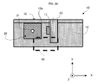
- FIG. 1 is a plan view of an optical scanning device; FIG. It is 1B arrow directional view of FIG. 1A.
- FIG. 1C is a view in the direction of arrow 1C of FIG. 1A;
- FIG. 1D is a view in the direction of arrow 1D of FIG. 1A;
- It is a side view of a support frame.
- FIG. 11 is a side view of the plate-like mirror being adjusted using a jig for angle adjustment; It is a figure which sees through and shows a jig
- FIG. 11 is a side view of the plate-like mirror being adjusted using a jig for angle adjustment; It is a figure which sees through and shows a jig
- FIG. 10 is a side view of the rotating mirror being adjusted using a jig; 4B is a perspective view of a jig in FIG. 4A;
- FIG. FIG. 4 is a diagram showing a configuration in which a correction prism is attached to the inner surface side of a transparent portion;
- FIG. 10 is a diagram showing a spectacles-type image display device as an application example of the optical scanning device;
- FIG. 11 is a side view of another optical scanning device;
- 7B is a perspective view of the optical scanning device of FIG. 7A;
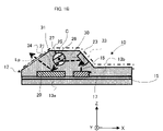
- FIG. 1A is a plan view of the optical scanning device 10
- FIG. 1B is a view on arrow 1B of FIG. 1A
- FIG. 1C is a view on arrow 1C of FIG. 1A
- FIG. 1D is a view on arrow 1D of FIG. 1A.
- 1A to 1D show the optical scanning device 10 with the cover 33 (one-dot chain line in FIG. 1B) removed.
- the optical scanning device 10 has a support frame 12 .
- the support frame 12 has an L-shaped cross-sectional contour, and has a bottom plate portion 13a and an upright plate portion 13b that are vertically connected.
- the substrate 15 has a rectangular shape and is placed and fixed on the upper surface of the bottom plate portion 13a.
- a three-axis orthogonal coordinate system is defined.
- the X-axis and Y-axis are defined as axes parallel to the longitudinal direction (parallel to the long sides) and the lateral direction (parallel to the short sides) of the substrate 15, respectively.
- the Z-axis is defined as an axis parallel to the upright direction of the upright plate portion 13 b from the substrate 15 .
- scanning light is emitted from the left side of FIG. 1B, that is, from the negative end of the optical scanning device 10 in the X-axis direction.
- the positive side and the negative side in the Z-axis direction of the substrate 15 are the upper surface and the lower surface, respectively, the positive side and the negative side in the Z-axis direction are appropriately defined as the upper side and the lower side of the optical scanning device 10 .
- the VCSEL 17 and the MEMS optical deflector 20 are mounted on the upper surface of the substrate 15 with the X-axis direction as the alignment direction.
- the VCSEL 17 has an emitting portion 18 on its upper surface, and emits laser light upward in parallel to the Z-axis direction from the emitting portion 18 .
- the MEMS optical deflector 20 directs the mirror surface of the rotating mirror 21 upward in the Z-axis direction.
- the MEMS optical deflector 20 is a two-dimensional scanning MEMS optical deflector in this embodiment, it may be a one-dimensional scanning MEMS optical deflector.
- Various configurations of the MEMS optical deflector itself are known. Deflectors) is selected.
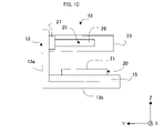
- FIG. 2 is a side view of the support frame 12.
- FIG. The support frame 12, the plate-like mirror 23 and the rotating mirror 25 will be described with reference to FIGS. 1A to 1D and FIG.
- the upright plate portion 13b of the support frame 12 has an inclined groove 30 and a through hole 31.
- the inclined groove 30 has a rectangular shape when viewed from the side in FIG. 2, and opens obliquely rearward upward along the side contour of the standing plate portion 13b.
- the bottom surface of the inclined groove 30 is formed with an inclined surface inclined at 45° with respect to the substrate 15 .
- the through hole 31 is formed as a cylindrical hole penetrating through the standing plate portion 13b in the Y-axis direction.
- the center of the width of the inclined surface (bottom surface) of the inclined groove 30 (length in side view in FIG. 1B) is located at the same position as the emitting portion 18 of the VCSEL 17 .
- the center line C of the cylindrical hole of the through hole 31 is located between the VCSEL 17 and the rotating mirror 21 of the MEMS optical deflector 20 in the X-axis direction.
- the center of the length of the inclined surface of the inclined groove 30 and the center line of the cylindrical hole of the through hole 31 are located at the same position, that is, at the same height from the substrate 15 .
- the plate-like mirror 23 is made of a rectangular plate-like member, and has one end portion adhered to the inclined surface portion of the inclined groove 30 in a cantilevered state with an adhesive member such as resin.
- the plate thickness of the plate-like mirror 23 is set substantially equal to the depth of the inclined groove 30 .
- the plate width of the plate-like mirror 23 (length in side view in FIG. 1B) is slightly shorter than the width of the inclined groove 30 (length in side view in FIG. 1B). Therefore, before one end of the plate-like mirror 23 is adhered to the inclined groove 30, that is, before the one end is fixed, the plate-like mirror 23 is slightly displaceable in the direction of the slope of the bottom surface within the inclined groove 30. In addition, the angle of rotation around the axis parallel to the Y-axis can be changed. Such a change makes it possible to adjust the orientation of the mirror surface of the plate-like mirror 23 when the optical scanning device 10 is manufactured.
- the rotary mirror 25 has a flat mirror portion 26 and a cylindrical fitting end portion 27 that is coupled to one end portion of the mirror portion 26 and fits into the through hole 31 .
- the diameter of the fitting end portion 27 is slightly smaller than the diameter of the through hole 31 . Therefore, before the fitting end portion 27 is adhered to the through hole 31 , that is, before being fixed, the rotary mirror 25 fits the fitting end portion 27 into the through hole 31 while adjusting the center line of the through hole 31 . , and can be tilted within a predetermined tilt angle range from a state in which the center line of the rotary mirror 25 is aligned with the center line of the through hole 31 . Therefore, it can be rotationally displaced in a larger angle range than the plate-like mirror 23 .
- Such a rotatable and tiltable configuration enables the orientation of the mirror surface of the mirror section 26 to be adjusted when the optical scanning device 10 is manufactured. After the adjustment, the fitting end portion 27 is adhered and fixed with an adhesive member such as resin.
- the rotary mirror 21 of the MEMS optical deflector 20 is not positioned directly below the rotary mirror 25 but is positioned on the front side, that is, on the negative side of the rotary mirror 25 in the X-axis direction.
- this configuration contributes to making the emission direction of the light Lp from the optical scanning device 10 not perpendicular to the substrate 15 but obliquely forward.
- the optical scanning device 10 when the optical scanning device 10 is attached to the temple of the eyeglass body as a video scanning device of smart glasses, the light emitted from the optical scanning device 10 can pass through a small gap between the imaging device and the user's face. It guarantees that the inner surface of the lens of the spectacle body can be reached without being interfered with by the user's face (Fig. 6).
- the plate-shaped mirror 23 and the rotary mirror 25 correspond to the first mirror and the second mirror of the optical manipulation device of the present invention, respectively.
- the plate-like mirror 23 and the rotating mirror 25 can be used as the second mirror and the first mirror of the optical manipulation device of the present invention, respectively, by reversing the supporting positions on the upright plate portion 13b. can also be equivalent. In that case, the positions of the inclined groove 30 and the through hole 31 in the X-axis direction are also reversed according to the change of the support position.
- the inclination angle of the plate-like mirror 23 is changed from 45° in the case of the first mirror to changed to about 24°.
- FIG. 6 is a diagram showing a spectacles-type image display device 155 as an application example of the optical scanning device 10.
- the glasses-type image display device 155 will be briefly described.
- the spectacles-type image display device 155 includes a spectacles main body 160 and the video generation device 110 detachably attached to the spectacles main body 160 with a clip 170 .
- the eyeglass body 160 includes left and right temples 161a and 161b, and a front frame 163 that is coupled to the front ends of the left and right temples 161a and 161b at both left and right ends.
- the front frame 163 further includes left and right lens frame portions 164a and 164b, and a bridge 165 connecting the left and right lens frame portions 164a and 164b.
- the optical scanning device 10 is incorporated in the image generating device 110 along the extension direction of the temple 161b of the spectacle body 160 along with other elements (eg, MEMS sensor buffer amplifier and LDD (laser driver)) arranged in a row.
- the optical scanning device 10 is arranged in the forefront, that is, closest to the lens 167 side.
- the light Lp (FIG. 2B) emitted from the optical scanning device 10 irradiates the inner surface of the lens 67 to generate an image in the scanning area 172 .
- the cover 33 extends along the contour of the upright plate portion 13b above the substrate 15, covers the upright plate portion 13b, and has the peripheral edge of the lower end fixed to the peripheral edge of the bottom plate portion 13a.
- the cover 33 has a transparent portion 34 at least in a portion where light Lp, which will be described later, is emitted from the optical scanning device 10 as scanning light.
- FIG. 5 shows a configuration in which a correction prism 54 is attached to the inner surface of the transparent portion 34.
- Reference numeral 56 denotes a scanning area generated at the irradiation destination by the light Lp emitted as scanning light from the transparent portion 34 of the optical scanning device 10 when the correction prism 54 is not provided.
- Reference numeral 58 denotes a scanning area generated at the irradiation destination by the light Lp emitted as the scanning light from the transparent portion 34 of the optical scanning device 10 when the correction prism 54 is present.
- the rotating mirror 21 of the MEMS optical deflector 20 rotates around the X axis and around the Y axis in resonance and non-resonance, respectively.
- the light Lp emitted from the rotating mirror 21 becomes scanning light for two-dimensional scanning.
- the resonant frequency and non-resonant frequency are, for example, 30 kHz to 40 kHz and 60 Hz to 120 Hz, respectively.
- the reciprocating rotation angle of the rotating mirror 21 about the X-axis is larger than the reciprocating rotating angle of the rotating mirror 21 about the Y-axis.
- the light Lp reciprocates in the Sx-axis direction in the pre-correction scanning area 56 or the post-correction scanning area 58.
- the light Lp When the correction prism 54 is not installed, the light Lp generates a pre-correction scanning area 56 on the scanning destination.
- the pre-correction scanning area 56 has a distorted shape with respect to the rectangle.
- the pre-correction scanning area 56 when the pre-correction scanning area 56 is provided, the light Lp produces a rectangular post-correction scanning area 58 in which the distortion is corrected.
- the post-correction scanning area 58 corresponds to the inscribed rectangle of the pre-correction scanning area 56 .
- the dashed line through which the light Lp is extracted indicates the optical path of the light Lp.
- the light Lp emitted from the emitting portion 18 of the VCSEL 17 is laser light sufficiently weakened so as not to harm human eyes.
- the light Lp is emitted from the emitting portion 18 of the VCSEL 17 perpendicularly to the substrate 15 and upward (positive direction in the Z-axis direction).
- the light Lp is incident on the plate-shaped mirror 23, it is reflected by the plate-shaped mirror 23, and the direction is parallel to the X-axis as the alignment direction of the VCSEL 17 and the output section 18 on the upper surface of the substrate 15. Make it negative and change it. Then, after traveling forward (negative side of the X axis) parallel to the X axis, the light is incident on the obliquely downward mirror surface of the mirror portion 26 of the rotary mirror 25 .
- the tilt angle of the mirror section 26 with respect to the substrate 15 is smaller than 45°. Therefore, the light Lp reflected by the mirror section 26 descends obliquely forward without descending to the substrate 15 in parallel with the Z-axis direction, that is, in the direction perpendicular to the substrate 15 , and the MEMS optical deflector 20 . The light enters the center of the rotating mirror 21 .
- the rotating mirror 21 rotates two-dimensionally. Therefore, the light Lp incident on the rotating mirror 21 becomes scanning light for two-dimensional scanning, and travels obliquely forward and upward from the rotating mirror 21 .
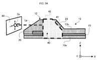
- FIG. 3A to 3D are explanatory diagrams when one end portion of the plate-like mirror 23 is attached to the bottom surface of the inclined groove 30 as the slope portion.
- FIG. 3A is a side view of the plate-like mirror 23 being adjusted using a jig 40 for adjusting the angle of the plate-like mirror 23, and
- FIG. 3B is a perspective view of the jig 40 in FIG. 3A.
- FIG. 3C is a view showing the optical scanning device 10 as seen from above in FIG. 3A
- FIG. 3D is a see-through view of the jig 40 in FIG. 3C.
- the plate-like mirror 23 is attached to the inclined groove 30 so that the angles of the three axes (X-axis, Y-axis and Z-axis) of the plate-like mirror 23 are appropriate, that is, the direction of the plate-like mirror 23 is appropriate. This is performed while the operator looks at the position of the light spot Sp on the screen 44 so as to be as follows.
- the optical scanning device 10 is mounted on a predetermined mounting work device before the plate-shaped mirror 23 is mounted. In the mounting state, the support frame 12 is fixed to the mounting device together with the board 15 .
- one end portion of the plate-like mirror 23 is inserted into the inclined groove 30, and the jig 40 is moved from the other end side of the plate-like mirror 23 to the lower surface side of the other end portion of the plate-like mirror 23, that is, the mirror surface side. is inserted into
- the jig 40 has an inclined surface 41 and an upper surface 42 .
- the jig 40 has an inclined surface 41 applied to the other end of the mirror surface of the plate-like mirror 23, and rotates the other end around an axis parallel to the Y-axis, and rotates the other end in the X-axis direction (optical scanning device 10 ) and the Z-axis direction (the height direction of the optical scanning device 10).
- the VCSEL 17 is in a lighting state during the position adjustment of the plate-like mirror 23 by the jig 40 . Therefore, the light spot Sp is generated on the screen 44, and the position of the light spot Sp on the screen 44 moves two-dimensionally as the jig 40 moves.
- the operator operates the jig 40 to move one end of the plate-like mirror 23 within the inclined groove 30 while looking at the position of the light spot Sp on the screen 44 . Then, when the light spot Sp reaches the set position on the screen 44, the jig 40 is operated to hold the plate-like mirror 23 in the orientation (attitude and position) at that time.
- the operator applies droplets of the adhesive to a plurality of locations so as to straddle between one end of the plate-like mirror 23 and the inclined groove 30 . .
- the plate-like mirror 23 is fixed to the inclined surface of the bottom wall of the inclined groove 30 in the direction when the light spot Sp is at the set position on the screen 44 .
- the mirror surface of the plate-like mirror 23 reflects the light Lp emitted from the emitting portion 18 of the VCSEL 17 toward the rotary mirror 25 in parallel with the X-axis.
- the plate-like mirror 23 is held stationary in an arbitrary direction while its one end is in contact with the inclined surface of the bottom wall of the inclined groove 30 , and the droplet of the adhesive is applied to the one end of the plate-like mirror 23 and the inclined groove 30 . If it is attached at a plurality of locations so as to straddle the gap, it can be fixed in any direction after the adhesive is dried.
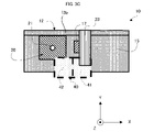
- FIG. 4A and 4B are explanatory diagrams when one end of the rotary mirror 25 is attached to the through hole 31.
- FIG. FIG. 4A is a side view when the position of the rotary mirror 25 is adjusted using a jig 47 for adjusting the orientation of the rotary mirror 25, and
- FIG. 4B is a perspective view of the jig 47 in FIG. 4A. It is a diagram.
- the jig 47 grips the other end of the mirror portion 26 and advances to the positive side in the Y-axis direction to fit the fitting end 27 into the through hole 31 .
- the jig 47 rotates the rotary mirror 25 around the center line of the through hole 31 so that the light spot Sp comes to the set position on the screen 51. adjust the angle. When the light spot Sp reaches the set position, the rotation of the rotary mirror 25 by the jig 47 is stopped.
- the operator stops moving the rotary mirror 25 and adheres one end of the plate-like mirror 23 to the inclined surface of the bottom surface of the inclined groove 30 .
- droplets of adhesive are deposited at a plurality of locations across the through hole 31 and the mating end 27 .
- the orientation of the rotary mirror 25 is adjusted to ensure that the light Lp emitted from the rotary mirror 21 of the MEMS optical deflector 20 is emitted in an appropriate direction.
- FIGS. 7A and 7B are side and perspective views, respectively, of an optical scanning device 70 that is another embodiment of the present invention. Elements in the optical scanning device 70 that are the same as those in the optical scanning device 10 of the above-described embodiment are denoted by the same reference numerals as those in the optical scanning device 10, and description thereof is omitted. .
- the difference between the optical scanning device 10 and the optical scanning device 70 is the rotation mechanism of the second mirror in the optical scanning device. That is, the rotary mirror 25 as the second mirror in the optical scanning device 10 is fitted into the through hole 31 of the support frame 12b at the end on the standing plate portion 13b side to adjust the rotation angle around the center line C. It is then fixed with adhesive. On the other hand, the plate-like mirror 75 as the second mirror of the optical scanning device 70 is fixed to the points 79 of the pair of edge members 78a and 78b by adhesion while being pressed from both sides thereof.
- the details of the fixing structure of the optical scanning device 70 are as follows.
- the edge members 78a and 78b are made of bar pieces with fan-shaped cross sections, and have their bases fixed to the upright plate portion 13b and protrude parallel to the substrate 15 from the upright plate portion 13b.
- the edge-like points 79 of the edge members 78a and 78b form edge lines as protruding ends of the fan-shaped cross section, and are opposed to each other with a gap corresponding to the plate thickness of the plate-like mirror 75. As shown in FIG.
- the plate-like mirror 75 is inserted into the gap between the points 79 with the mirror surface side as the lower surface, and is maintained rotatable about the center line of the gap between the points 79 before being fixed to the points 79 by adhesion. , and both points 79 from both sides with a predetermined clamping force. After that, the plate-like mirror 75 has its rotation angle adjusted by the method described with reference to FIGS. 4A and 4B. That is, the plate-like mirror 75 is adjusted to a rotation angle that forms the light spot Sp at the target position of the screen 51 when the light Lp from the plate-like mirror 23 is reflected by the mirror surface of the plate-like mirror 75 . After the adjustment, the plate-like mirror 75 is fixed to both points 79 by adhesion, and the rotation angle is fixed.
- the through hole 31 of the upright plate portion 13b having the fitting end portion 27 as one end portion of the rotary mirror 25 as a second support portion has a cylindrical hole as a body of rotation with the center line of the through hole 31 as the center line. .
- the rotational position of the rotary mirror 25 around the center of the through-hole 31 can be accurately set as one of the positioning of the rotary mirror 25 when the optical scanning device 10 is manufactured.
- the shape of the through hole 31 is a cylinder.
- a fitting end portion 27 as one end portion of the rotary mirror 25 is fixed to the through hole 31 by adhesion.
- adhesion it is possible to adjust the adhesion position of the adhesive in the adhesion part and change the distribution of the adhesion amount. Therefore, during manufacturing, not only the rotational position of the mirror portion 26 of the rotary mirror 25 around the axis of the through hole 31 but also various other positions are adjusted to optimize the orientation of the rotary mirror 25. It can be fixed to the standing plate portion 13b.
- the through-hole 31 is a truncated cone tapered toward the end in the direction in which the fitting end 27 is inserted into the through-hole 31, the positioning of the through-hole 31 in the direction of the center line C of the cylindrical hole is performed at the time of manufacture. can be simplified.
- the light Lp emitted from the VCSEL 17 perpendicularly to the substrate 15 is reflected on the substrate 15 in a direction parallel to the direction in which the VCSEL 17 and the MEMS optical deflector 20 are arranged.
- the part is adhered to the slanted surface which is the bottom of the slanted groove 30 .
- Adhesion can easily change not only the tilt angle of the inclined surface but also the orientation of the plate-like mirror 23 in various directions within a small range by adjusting the adhesion position and the adhesion amount (uplift amount) at the adhesion position. . Thereby, the orientation of the plate-like mirror 23 can be accurately adjusted to a desired orientation.
- the rotary mirror 21 of the MEMS optical deflector 20 is arranged away from the rotary mirror 25 in the X-axis direction, not directly below the rotary mirror 25, the light Lp as the scanning light is directed to the substrate 15. It can be emitted obliquely instead of vertically.
- the optical scanning device 10 is attached to the temples of the glasses and used as smart glasses, such an emission direction allows the scanning area of the scanning light to pass through the narrow gap between the user's face and the temples of the glasses.
- it can be formed on the inner surface of the lens.
- the fitting end portion fitting end portion 27 and the through hole through hole 31 in the optical scanning device 10 and the pair of edge members 78 in the optical scanning device 70 correspond to the rotation mechanism of the present invention.
- the fixing member is an adhesive member, but a fastening member other than the adhesive member, such as screws, can be selected as appropriate.
- the optical scanning device 10 includes a VCSEL 17.
- the VCSEL 17 is an example of a surface emitting laser element.
- the present invention can employ a laser light source other than a vertical cavity surface emitting laser (VCSEL: Vertical Cavity Surface Emitting Laser) as long as it is a surface emitting laser element.
- VCSEL Vertical Cavity Surface Emitting Laser
- the upright plate portion 13b of the support frame 12 is an example of a plate-shaped support member fixed to the substrate 15.
- the upright plate portion 13b is fixed to the substrate 15 via the bottom plate portion 13a, but the plate-like support member of the present invention can also be fixed directly to the substrate.
- the plate-like mirror 23 and the rotary mirror 25 or the plate-like mirror 75 as the first mirror and the second mirror have one end in the Y-axis direction as the second axis direction. 13b, the other end is a free end and is fixed in a cantilevered state.
- the first mirror and the second mirror of the present invention may be supported on both sides when the optical scanning devices 10 and 70 are completed.
- the inclined groove 30 having the bottom surface as the first support portion may also be a through hole in the shape of a rotating body.
- the first support portion a through hole in the shape of a rotating body, and make the second support portion an inclined surface portion.
- the X-, Y-, and Z-axes are defined as corresponding to the first, second, and third axes of the present invention, respectively, but this is only for the optical scanning device of the embodiment. 10 is defined as such for convenience of explanation.
- the optical scanning device 10 can be applied as an image generation device in smart glasses, and can also be applied as an image generation device in an ultra-compact projector or an interactive projector.
- the optical scanning device 10 can control the intensity of the light Lp emitted from the VCSEL 17 to generate an image in the scanning area. However, since the optical scanning device 10 of the embodiment is equipped with only one VCSEL 17, it can only generate a monochrome image. When generating a color image, the optical scanning device 10 must be equipped with a total of three VCSELs 17 that output light corresponding to the three primary colors.
- the three VCSELs 17 for each color are mounted on the substrate 15 so as to be aligned in the X-axis direction together with the MEMS optical deflector 20, and the three plate-like mirrors 23 are arranged at the same height just above the three VCSELs 17 in the X direction. Arrange them in a row in the axial direction.
- the first and second plate-shaped mirrors 23 from the closest side to the rotary mirror 25 serve as half mirrors, and the light enters from the second and third plate-shaped mirrors 23 as half mirrors.
- the incoming light Lp is made to go straight as it is to the rotary mirror 25.
- the rotating mirror 21 and the plate-like mirror 23 are each supported in a cantilever manner with respect to one upright plate portion 13b, but the present invention is not limited to this.
- the rotatable mirror 21 and the plate-like mirror 23 may be supported by the two facing upright plate portions 13b. It doesn't matter if each one supports it.
- the standing plate portion 13b may be a wall surface of the housing of the optical scanning device 10 instead of an independent plate portion.
- Reference numerals 10, 70 optical scanning device, 13b: standing plate portion (plate-like support member), 15: substrate, 17: VCSEL (surface emitting laser element), 20: MEMS light deflection Device 21... Rotary mirror 23, 75... Plate-shaped mirror 25... Rotating mirror 26... Mirror part 27... Fitting end (one end) 30. Inclined groove (slant surface), 31 through hole.
Landscapes
- Physics & Mathematics (AREA)
- General Physics & Mathematics (AREA)
- Optics & Photonics (AREA)
- Mechanical Optical Scanning Systems (AREA)
- Mechanical Light Control Or Optical Switches (AREA)
- Micromachines (AREA)
Abstract
Description
基板と、
出射方向を前記基板に対して上向きにして前記基板上に実装された面発光レーザ素子と、
回動ミラーを前記基板に対して上向きにして前記基板上に実装されたMEMS光偏向器と、
前記基板に固定された板状支持部材と、
前記基板上の前記面発光レーザ素子及び前記MEMS光偏向器の並び方向としての第1軸方向に対して垂直でかつ前記基板に対して平行な第2軸方向に延在し、前記面発光レーザ素子からの出射光を前記第1軸方向に反射するように前記板状支持部材の第1支持部に支持されている第1ミラーと、
前記第2軸方向に延在し、前記第1ミラーからの光を前記MEMS光偏向器の前記回動ミラーに向けて反射するように、前記板状支持部材の第2支持部に支持されている第2ミラーと、
を備え、
前記第1支持部及び前記第2支持部のうちの少なくとも一方の支持部は、当該一方の支持部が支持している前記第1ミラー及び前記第2ミラーの一方のミラーを回転可能に支持する回動機構と前記回動機構における前記一方のミラーの回動位置を固定する固定部材とを含む。
図1Aは光走査装置10の平面図、図1Bは図1Aの1B矢視図、図1Cは図1Aの1C矢視図、図1Dは図1Aの1D矢視図である。なお、図1A-図1Dは、カバー33(図1Bの一点鎖線)を取り外した状態で光走査装置10を示している。
図5は、透明部34の内面側に補正プリズム54を取り付けた構成を示している。なお、56は、補正プリズム54の無しの場合に、光走査装置10の透明部34から走査光として出射した光Lpが照射先において生成する走査領域を示している。58は、補正プリズム54の有りの場合に、光走査装置10の透明部34から走査光として出射した光Lpが照射先において生成する走査領域を示している。
図1Bにおいて、光Lpが引き出されている破線は、光Lpの光路を示している。なお、VCSEL17の出射部18から出射する光Lpは、人の目に害を与えない程度に十分に弱めたレーザ光である。
図3A-図3D及び図4A-図4Bを参照して、光走査装置10の製造時における板状ミラー23及び回転型ミラー25の取付方法について説明する。
図7A及び図7Bは、それぞれ本発明の別の実施形態である光走査装置70の側面図及び斜視図である。光走査装置70において、前述の実施形態である光走査装置10の要素と同一の要素については、光走査装置10の要素と同一の符号を付けているとともに、説明は省略する。。
回転型ミラー25の一端部としての嵌合端部27を第2支持部としての起立板部13bの貫通孔31は、貫通孔31の中心線を中心線とする回転体としての円柱孔を有する。この結果、光走査装置10の製造時に、回転型ミラー25の位置決めの1つとしての貫通孔31の中心の回りの回転型ミラー25の回転位置を正確に設定することができる。
光走査装置10における嵌合端部嵌合端部27及び貫通孔貫通孔31と、光走査装置70における1対のエッジ部材78とは、本発明の回動機構に相当する。実施形態では、固定部材は、接着部材となっているが、ビス等の接着部材以外の留め部材を適宜選択することもできる。
Claims (6)
- 基板と、
出射方向を前記基板に対して上向きにして前記基板上に実装された面発光レーザ素子と、
回動ミラーを前記基板に対して上向きにして前記基板上に実装されたMEMS光偏向器と、
前記基板に固定された板状支持部材と、
前記基板上の前記面発光レーザ素子及び前記MEMS光偏向器の並び方向としての第1軸方向に対して垂直でかつ前記基板に対して平行な第2軸方向に延在し、前記面発光レーザ素子からの出射光を前記第1軸方向に反射するように前記板状支持部材の第1支持部に支持されている第1ミラーと、
前記第2軸方向に延在し、前記第1ミラーからの光を前記MEMS光偏向器の前記回動ミラーに向けて反射するように、前記板状支持部材の第2支持部に支持されている第2ミラーと、
を備え、
前記第1支持部及び前記第2支持部のうちの少なくとも一方の支持部は、当該一方の支持部が支持している前記第1ミラー及び前記第2ミラーの一方のミラーを回転可能に支持する回動機構と前記回動機構における前記一方のミラーの回動位置を固定する固定部材とを含むことを特徴とする光走査装置。 - 請求項1記載の光走査装置において、
前記回動機構は、前記一方のミラーの一端部が挿入されて支持された貫通孔を有し、
前記貫通孔は、前記第2軸方向の軸線を中心線とする回転体の形状を有することを特徴とする光走査装置。 - 請求項2記載の光走査装置において、
前記固定部材は、接着剤を含むことを特徴とする光走査装置。 - 請求項2又は3記載の光走査装置において、
前記貫通孔の形状は、円柱、又は前記一方のミラーの一端部の挿入方向の先に向かってつぼまる円錐台であり、
前記一方の支持部と、前記一方の支持部に支持される前記一端部とは、相互に接着されていることを特徴とする光走査装置。 - 請求項1~4記載のいずれか1項に記載の光走査装置において、
前記一方の支持部は前記第2支持部であり、
前記第1支持部は、前記板状支持部材に形成された斜面を有し、
前記第1ミラーの一端部は、前記第1ミラーが前記面発光レーザ素子からの入射光を前記第1軸方向に対して平行に反射するように、前記斜面に接着されていることを特徴とする光走査装置。 - 請求項1~5のいずれか1項に記載の光走査装置において、
前記回動ミラーは、前記第1軸方向に前記第2ミラーに対して前記第1ミラーとは反対側に配置され、前記第2ミラーからの光を、前記基板に対して傾斜する傾斜角で前記第1軸方向に前記第2ミラーとは反対側に反射することを特徴とする光走査装置。
Priority Applications (3)
| Application Number | Priority Date | Filing Date | Title |
|---|---|---|---|
| US18/273,457 US12504622B2 (en) | 2021-02-22 | 2022-01-24 | Optical scanning device |
| EP22755840.0A EP4270084B1 (en) | 2021-02-22 | 2022-01-24 | Optical scanning device |
| CN202280015867.7A CN116964505A (zh) | 2021-02-22 | 2022-01-24 | 光扫描装置 |
Applications Claiming Priority (2)
| Application Number | Priority Date | Filing Date | Title |
|---|---|---|---|
| JP2021026244A JP7529587B2 (ja) | 2021-02-22 | 2021-02-22 | 光走査装置 |
| JP2021-026244 | 2021-02-22 |
Publications (1)
| Publication Number | Publication Date |
|---|---|
| WO2022176516A1 true WO2022176516A1 (ja) | 2022-08-25 |
Family
ID=82931534
Family Applications (1)
| Application Number | Title | Priority Date | Filing Date |
|---|---|---|---|
| PCT/JP2022/002450 Ceased WO2022176516A1 (ja) | 2021-02-22 | 2022-01-24 | 光走査装置 |
Country Status (5)
| Country | Link |
|---|---|
| US (1) | US12504622B2 (ja) |
| EP (1) | EP4270084B1 (ja) |
| JP (2) | JP7529587B2 (ja) |
| CN (1) | CN116964505A (ja) |
| WO (1) | WO2022176516A1 (ja) |
Families Citing this family (2)
| Publication number | Priority date | Publication date | Assignee | Title |
|---|---|---|---|---|
| JP7643887B2 (ja) * | 2021-02-22 | 2025-03-11 | スタンレー電気株式会社 | 眼鏡型映像表示装置 |
| JP7641815B2 (ja) * | 2021-05-13 | 2025-03-07 | スタンレー電気株式会社 | 光走査装置及び製造方法 |
Citations (8)
| Publication number | Priority date | Publication date | Assignee | Title |
|---|---|---|---|---|
| US6002507A (en) * | 1998-12-01 | 1999-12-14 | Xerox Corpoation | Method and apparatus for an integrated laser beam scanner |
| KR100648929B1 (ko) * | 2005-07-27 | 2006-11-27 | 삼성전자주식회사 | 레이저 프로젝터 |
| US7428995B1 (en) * | 1993-10-25 | 2008-09-30 | Symbol Technologies, Inc. | Scanning devices and methods using surface emitting laser diodes |
| JP2009244869A (ja) | 2008-03-11 | 2009-10-22 | Panasonic Corp | 表示装置、表示方法、眼鏡型ヘッドマウントディスプレイ、及び自動車 |
| JP2010175677A (ja) | 2009-01-28 | 2010-08-12 | Hoya Corp | スキャナモジュールを備えたカメラ |
| JP2014056020A (ja) | 2012-09-11 | 2014-03-27 | Stanley Electric Co Ltd | 光偏向器 |
| JP2017207630A (ja) | 2016-05-18 | 2017-11-24 | スタンレー電気株式会社 | 光偏向器 |
| CN109437088A (zh) * | 2018-10-30 | 2019-03-08 | 苏州晶方半导体科技股份有限公司 | 芯片的封装结构以及封装方法 |
Family Cites Families (27)
| Publication number | Priority date | Publication date | Assignee | Title |
|---|---|---|---|---|
| JPS56120255U (ja) * | 1980-02-16 | 1981-09-12 | ||
| US5347121A (en) | 1992-12-18 | 1994-09-13 | Spectra-Physics Scanning Systems, Inc. | Variable focus optical system for data reading |
| US6715685B2 (en) | 1993-11-17 | 2004-04-06 | Symbol Technologies, Inc. | Optical path design for scanning assembly in compact bar code readers |
| US6014240A (en) * | 1998-12-01 | 2000-01-11 | Xerox Corporation | Method and apparatus for an integrated laser beam scanner using a carrier substrate |
| US6532093B2 (en) | 2000-12-06 | 2003-03-11 | Xerox Corporation | Integrated micro-opto-electro-mechanical laser scanner |
| WO2003019463A1 (en) | 2001-08-31 | 2003-03-06 | Optoelectronics Co., Ltd. | Module for optical information reader |
| WO2003040803A2 (en) | 2001-11-06 | 2003-05-15 | Keyotee | Apparatus for image projection |
| JP2006194973A (ja) | 2005-01-11 | 2006-07-27 | Fuji Xerox Co Ltd | 光走査装置 |
| JP4965935B2 (ja) | 2006-08-24 | 2012-07-04 | キヤノン株式会社 | 光偏向器、光走査装置及び走査型画像表示装置 |
| JP5466807B2 (ja) * | 2006-09-26 | 2014-04-09 | 株式会社トプコン | レーザスキャナ |
| WO2009041055A1 (ja) * | 2007-09-26 | 2009-04-02 | Panasonic Corporation | ビーム走査型表示装置、その表示方法、プログラム、及び集積回路 |
| US20100149073A1 (en) | 2008-11-02 | 2010-06-17 | David Chaum | Near to Eye Display System and Appliance |
| JP2010117542A (ja) | 2008-11-13 | 2010-05-27 | Panasonic Corp | ビーム走査型表示装置 |
| JP5361010B2 (ja) | 2011-03-29 | 2013-12-04 | 京セラドキュメントソリューションズ株式会社 | 光走査装置及びこれを備えた画像形成装置 |
| JP5909334B2 (ja) | 2011-07-29 | 2016-04-26 | 株式会社日立エルジーデータストレージ | 光ビーム走査装置およびそれを用いた画像表示装置 |
| US8891147B2 (en) | 2011-05-27 | 2014-11-18 | Hitachi-Lg Data Storage, Inc. | Optical beam scanning device and image display device using the same |
| JP2013046143A (ja) | 2011-08-23 | 2013-03-04 | Brother Ind Ltd | ヘッドマウント装置及び装着フレーム |
| US20140146394A1 (en) | 2012-11-28 | 2014-05-29 | Nigel David Tout | Peripheral display for a near-eye display device |
| JP2015022158A (ja) * | 2013-07-19 | 2015-02-02 | 株式会社リコー | 光走査装置および画像表示装置 |
| CN107438796B (zh) * | 2014-12-26 | 2020-07-03 | Cy视觉公司 | 头戴式显示装置、近眼显示装置和方法 |
| JP6734532B2 (ja) | 2016-04-22 | 2020-08-05 | ミツミ電機株式会社 | 表示装置 |
| JP7010226B2 (ja) * | 2016-08-19 | 2022-01-26 | ソニーグループ株式会社 | 光源モジュールおよび光源モジュールの製造方法ならびに投射型表示装置 |
| JP6227177B1 (ja) | 2017-01-20 | 2017-11-08 | 株式会社Qdレーザ | 画像投影装置 |
| US10338400B2 (en) | 2017-07-03 | 2019-07-02 | Holovisions LLC | Augmented reality eyewear with VAPE or wear technology |
| US11238143B2 (en) | 2018-06-05 | 2022-02-01 | Google Llc | Method and system for authenticating a user on a wearable heads-up display |
| JP7052577B2 (ja) | 2018-06-07 | 2022-04-12 | 株式会社リコー | 光学装置、映像表示装置、及び検眼装置 |
| CN111123522A (zh) * | 2020-01-17 | 2020-05-08 | 光感(上海)科技有限公司 | 一种增强现实眼镜的光学系统 |
-
2021
- 2021-02-22 JP JP2021026244A patent/JP7529587B2/ja active Active
-
2022
- 2022-01-24 US US18/273,457 patent/US12504622B2/en active Active
- 2022-01-24 WO PCT/JP2022/002450 patent/WO2022176516A1/ja not_active Ceased
- 2022-01-24 EP EP22755840.0A patent/EP4270084B1/en active Active
- 2022-01-24 CN CN202280015867.7A patent/CN116964505A/zh active Pending
-
2024
- 2024-07-25 JP JP2024119230A patent/JP7734804B2/ja active Active
Patent Citations (8)
| Publication number | Priority date | Publication date | Assignee | Title |
|---|---|---|---|---|
| US7428995B1 (en) * | 1993-10-25 | 2008-09-30 | Symbol Technologies, Inc. | Scanning devices and methods using surface emitting laser diodes |
| US6002507A (en) * | 1998-12-01 | 1999-12-14 | Xerox Corpoation | Method and apparatus for an integrated laser beam scanner |
| KR100648929B1 (ko) * | 2005-07-27 | 2006-11-27 | 삼성전자주식회사 | 레이저 프로젝터 |
| JP2009244869A (ja) | 2008-03-11 | 2009-10-22 | Panasonic Corp | 表示装置、表示方法、眼鏡型ヘッドマウントディスプレイ、及び自動車 |
| JP2010175677A (ja) | 2009-01-28 | 2010-08-12 | Hoya Corp | スキャナモジュールを備えたカメラ |
| JP2014056020A (ja) | 2012-09-11 | 2014-03-27 | Stanley Electric Co Ltd | 光偏向器 |
| JP2017207630A (ja) | 2016-05-18 | 2017-11-24 | スタンレー電気株式会社 | 光偏向器 |
| CN109437088A (zh) * | 2018-10-30 | 2019-03-08 | 苏州晶方半导体科技股份有限公司 | 芯片的封装结构以及封装方法 |
Non-Patent Citations (1)
| Title |
|---|
| See also references of EP4270084A4 |
Also Published As
| Publication number | Publication date |
|---|---|
| US12504622B2 (en) | 2025-12-23 |
| EP4270084B1 (en) | 2025-03-05 |
| JP2022127979A (ja) | 2022-09-01 |
| EP4270084A4 (en) | 2024-06-12 |
| JP2024138081A (ja) | 2024-10-07 |
| JP7734804B2 (ja) | 2025-09-05 |
| CN116964505A (zh) | 2023-10-27 |
| US20240103263A1 (en) | 2024-03-28 |
| EP4270084A1 (en) | 2023-11-01 |
| JP7529587B2 (ja) | 2024-08-06 |
Similar Documents
| Publication | Publication Date | Title |
|---|---|---|
| JP7734804B2 (ja) | 光走査装置 | |
| US9182600B2 (en) | Image display apparatus and head-mounted display | |
| US9229224B2 (en) | Image display apparatus and head-mounted display | |
| CN110462488B (zh) | 平视显示器装置 | |
| US9170422B2 (en) | Image display apparatus and head-mounted display | |
| US12311622B2 (en) | Method of final assembly of a light projector module | |
| JPH09146026A (ja) | 像面湾曲の補正方法および該方法に使用する光ビーム走査装置 | |
| EP4325269A1 (en) | Optical scanning device | |
| US12276785B2 (en) | Two-axis beam scanning systems and display systems with multiple beam scanners | |
| JP7643887B2 (ja) | 眼鏡型映像表示装置 | |
| US6922296B2 (en) | Optical path adjusting device | |
| US12461360B2 (en) | Movable device, projection apparatus, and head-up display | |
| WO2022239606A1 (ja) | 光走査装置及び製造方法 | |
| JP2020197682A (ja) | 光学素子調整機構および光学素子調整方法 | |
| JP2003075756A (ja) | 光走査装置 | |
| JP2007304442A (ja) | 網膜走査装置 |
Legal Events
| Date | Code | Title | Description |
|---|---|---|---|
| 121 | Ep: the epo has been informed by wipo that ep was designated in this application |
Ref document number: 22755840 Country of ref document: EP Kind code of ref document: A1 |
|
| WWE | Wipo information: entry into national phase |
Ref document number: 18273457 Country of ref document: US |
|
| ENP | Entry into the national phase |
Ref document number: 2022755840 Country of ref document: EP Effective date: 20230724 |
|
| WWE | Wipo information: entry into national phase |
Ref document number: 202280015867.7 Country of ref document: CN |
|
| NENP | Non-entry into the national phase |
Ref country code: DE |