WO2022176624A1 - 電力変換システム - Google Patents
電力変換システム Download PDFInfo
- Publication number
- WO2022176624A1 WO2022176624A1 PCT/JP2022/004110 JP2022004110W WO2022176624A1 WO 2022176624 A1 WO2022176624 A1 WO 2022176624A1 JP 2022004110 W JP2022004110 W JP 2022004110W WO 2022176624 A1 WO2022176624 A1 WO 2022176624A1
- Authority
- WO
- WIPO (PCT)
- Prior art keywords
- power conversion
- converter
- inverter
- conversion system
- voltage
- Prior art date
- Legal status (The legal status is an assumption and is not a legal conclusion. Google has not performed a legal analysis and makes no representation as to the accuracy of the status listed.)
- Ceased
Links
Images






Classifications
-
- H—ELECTRICITY
- H02—GENERATION; CONVERSION OR DISTRIBUTION OF ELECTRIC POWER
- H02M—APPARATUS FOR CONVERSION BETWEEN AC AND AC, BETWEEN AC AND DC, OR BETWEEN DC AND DC, AND FOR USE WITH MAINS OR SIMILAR POWER SUPPLY SYSTEMS; CONVERSION OF DC OR AC INPUT POWER INTO SURGE OUTPUT POWER; CONTROL OR REGULATION THEREOF
- H02M5/00—Conversion of AC power input into AC power output, e.g. for change of voltage, for change of frequency, for change of number of phases
- H02M5/40—Conversion of AC power input into AC power output, e.g. for change of voltage, for change of frequency, for change of number of phases with intermediate conversion into DC
- H02M5/42—Conversion of AC power input into AC power output, e.g. for change of voltage, for change of frequency, for change of number of phases with intermediate conversion into DC by static converters
- H02M5/44—Conversion of AC power input into AC power output, e.g. for change of voltage, for change of frequency, for change of number of phases with intermediate conversion into DC by static converters using discharge tubes or semiconductor devices to convert the intermediate DC into AC
- H02M5/453—Conversion of AC power input into AC power output, e.g. for change of voltage, for change of frequency, for change of number of phases with intermediate conversion into DC by static converters using discharge tubes or semiconductor devices to convert the intermediate DC into AC using devices of a triode or transistor type requiring continuous application of a control signal
- H02M5/458—Conversion of AC power input into AC power output, e.g. for change of voltage, for change of frequency, for change of number of phases with intermediate conversion into DC by static converters using discharge tubes or semiconductor devices to convert the intermediate DC into AC using devices of a triode or transistor type requiring continuous application of a control signal using semiconductor devices only
- H02M5/4585—Conversion of AC power input into AC power output, e.g. for change of voltage, for change of frequency, for change of number of phases with intermediate conversion into DC by static converters using discharge tubes or semiconductor devices to convert the intermediate DC into AC using devices of a triode or transistor type requiring continuous application of a control signal using semiconductor devices only having a rectifier with controlled elements
-
- H—ELECTRICITY
- H02—GENERATION; CONVERSION OR DISTRIBUTION OF ELECTRIC POWER
- H02M—APPARATUS FOR CONVERSION BETWEEN AC AND AC, BETWEEN AC AND DC, OR BETWEEN DC AND DC, AND FOR USE WITH MAINS OR SIMILAR POWER SUPPLY SYSTEMS; CONVERSION OF DC OR AC INPUT POWER INTO SURGE OUTPUT POWER; CONTROL OR REGULATION THEREOF
- H02M5/00—Conversion of AC power input into AC power output, e.g. for change of voltage, for change of frequency, for change of number of phases
- H02M5/40—Conversion of AC power input into AC power output, e.g. for change of voltage, for change of frequency, for change of number of phases with intermediate conversion into DC
- H02M5/42—Conversion of AC power input into AC power output, e.g. for change of voltage, for change of frequency, for change of number of phases with intermediate conversion into DC by static converters
- H02M5/44—Conversion of AC power input into AC power output, e.g. for change of voltage, for change of frequency, for change of number of phases with intermediate conversion into DC by static converters using discharge tubes or semiconductor devices to convert the intermediate DC into AC
- H02M5/453—Conversion of AC power input into AC power output, e.g. for change of voltage, for change of frequency, for change of number of phases with intermediate conversion into DC by static converters using discharge tubes or semiconductor devices to convert the intermediate DC into AC using devices of a triode or transistor type requiring continuous application of a control signal
- H02M5/458—Conversion of AC power input into AC power output, e.g. for change of voltage, for change of frequency, for change of number of phases with intermediate conversion into DC by static converters using discharge tubes or semiconductor devices to convert the intermediate DC into AC using devices of a triode or transistor type requiring continuous application of a control signal using semiconductor devices only
-
- B—PERFORMING OPERATIONS; TRANSPORTING
- B60—VEHICLES IN GENERAL
- B60L—PROPULSION OF ELECTRICALLY-PROPELLED VEHICLES; SUPPLYING ELECTRIC POWER FOR AUXILIARY EQUIPMENT OF ELECTRICALLY-PROPELLED VEHICLES; ELECTRODYNAMIC BRAKE SYSTEMS FOR VEHICLES IN GENERAL; MAGNETIC SUSPENSION OR LEVITATION FOR VEHICLES; MONITORING OPERATING VARIABLES OF ELECTRICALLY-PROPELLED VEHICLES; ELECTRIC SAFETY DEVICES FOR ELECTRICALLY-PROPELLED VEHICLES
- B60L50/00—Electric propulsion with power supplied within the vehicle
- B60L50/50—Electric propulsion with power supplied within the vehicle using propulsion power supplied by batteries or fuel cells
- B60L50/51—Electric propulsion with power supplied within the vehicle using propulsion power supplied by batteries or fuel cells characterised by AC-motors
-
- H—ELECTRICITY
- H02—GENERATION; CONVERSION OR DISTRIBUTION OF ELECTRIC POWER
- H02M—APPARATUS FOR CONVERSION BETWEEN AC AND AC, BETWEEN AC AND DC, OR BETWEEN DC AND DC, AND FOR USE WITH MAINS OR SIMILAR POWER SUPPLY SYSTEMS; CONVERSION OF DC OR AC INPUT POWER INTO SURGE OUTPUT POWER; CONTROL OR REGULATION THEREOF
- H02M1/00—Details of apparatus for conversion
- H02M1/0043—Converters switched with a phase shift, i.e. interleaved
-
- H—ELECTRICITY
- H02—GENERATION; CONVERSION OR DISTRIBUTION OF ELECTRIC POWER
- H02M—APPARATUS FOR CONVERSION BETWEEN AC AND AC, BETWEEN AC AND DC, OR BETWEEN DC AND DC, AND FOR USE WITH MAINS OR SIMILAR POWER SUPPLY SYSTEMS; CONVERSION OF DC OR AC INPUT POWER INTO SURGE OUTPUT POWER; CONTROL OR REGULATION THEREOF
- H02M1/00—Details of apparatus for conversion
- H02M1/08—Circuits specially adapted for the generation of control voltages for semiconductor devices incorporated in static converters
-
- H—ELECTRICITY
- H02—GENERATION; CONVERSION OR DISTRIBUTION OF ELECTRIC POWER
- H02M—APPARATUS FOR CONVERSION BETWEEN AC AND AC, BETWEEN AC AND DC, OR BETWEEN DC AND DC, AND FOR USE WITH MAINS OR SIMILAR POWER SUPPLY SYSTEMS; CONVERSION OF DC OR AC INPUT POWER INTO SURGE OUTPUT POWER; CONTROL OR REGULATION THEREOF
- H02M1/00—Details of apparatus for conversion
- H02M1/14—Arrangements for reducing ripples from DC input or output
-
- H—ELECTRICITY
- H02—GENERATION; CONVERSION OR DISTRIBUTION OF ELECTRIC POWER
- H02M—APPARATUS FOR CONVERSION BETWEEN AC AND AC, BETWEEN AC AND DC, OR BETWEEN DC AND DC, AND FOR USE WITH MAINS OR SIMILAR POWER SUPPLY SYSTEMS; CONVERSION OF DC OR AC INPUT POWER INTO SURGE OUTPUT POWER; CONTROL OR REGULATION THEREOF
- H02M7/00—Conversion of AC power input into DC power output; Conversion of DC power input into AC power output
- H02M7/42—Conversion of DC power input into AC power output without possibility of reversal
- H02M7/44—Conversion of DC power input into AC power output without possibility of reversal by static converters
- H02M7/48—Conversion of DC power input into AC power output without possibility of reversal by static converters using discharge tubes with control electrode or semiconductor devices with control electrode
- H02M7/4815—Resonant converters
- H02M7/4818—Resonant converters with means for adaptation of resonance frequency, e.g. by modification of capacitance or inductance of resonance circuits
-
- H—ELECTRICITY
- H02—GENERATION; CONVERSION OR DISTRIBUTION OF ELECTRIC POWER
- H02M—APPARATUS FOR CONVERSION BETWEEN AC AND AC, BETWEEN AC AND DC, OR BETWEEN DC AND DC, AND FOR USE WITH MAINS OR SIMILAR POWER SUPPLY SYSTEMS; CONVERSION OF DC OR AC INPUT POWER INTO SURGE OUTPUT POWER; CONTROL OR REGULATION THEREOF
- H02M7/00—Conversion of AC power input into DC power output; Conversion of DC power input into AC power output
- H02M7/42—Conversion of DC power input into AC power output without possibility of reversal
- H02M7/44—Conversion of DC power input into AC power output without possibility of reversal by static converters
- H02M7/48—Conversion of DC power input into AC power output without possibility of reversal by static converters using discharge tubes with control electrode or semiconductor devices with control electrode
- H02M7/53—Conversion of DC power input into AC power output without possibility of reversal by static converters using discharge tubes with control electrode or semiconductor devices with control electrode using devices of a triode or transistor type requiring continuous application of a control signal
- H02M7/537—Conversion of DC power input into AC power output without possibility of reversal by static converters using discharge tubes with control electrode or semiconductor devices with control electrode using devices of a triode or transistor type requiring continuous application of a control signal using semiconductor devices only, e.g. single switched pulse inverters
- H02M7/539—Conversion of DC power input into AC power output without possibility of reversal by static converters using discharge tubes with control electrode or semiconductor devices with control electrode using devices of a triode or transistor type requiring continuous application of a control signal using semiconductor devices only, e.g. single switched pulse inverters with automatic control of output wave form or frequency
- H02M7/5395—Conversion of DC power input into AC power output without possibility of reversal by static converters using discharge tubes with control electrode or semiconductor devices with control electrode using devices of a triode or transistor type requiring continuous application of a control signal using semiconductor devices only, e.g. single switched pulse inverters with automatic control of output wave form or frequency by pulse-width modulation
-
- B—PERFORMING OPERATIONS; TRANSPORTING
- B60—VEHICLES IN GENERAL
- B60L—PROPULSION OF ELECTRICALLY-PROPELLED VEHICLES; SUPPLYING ELECTRIC POWER FOR AUXILIARY EQUIPMENT OF ELECTRICALLY-PROPELLED VEHICLES; ELECTRODYNAMIC BRAKE SYSTEMS FOR VEHICLES IN GENERAL; MAGNETIC SUSPENSION OR LEVITATION FOR VEHICLES; MONITORING OPERATING VARIABLES OF ELECTRICALLY-PROPELLED VEHICLES; ELECTRIC SAFETY DEVICES FOR ELECTRICALLY-PROPELLED VEHICLES
- B60L2200/00—Type of vehicles
- B60L2200/10—Air crafts
-
- B—PERFORMING OPERATIONS; TRANSPORTING
- B60—VEHICLES IN GENERAL
- B60L—PROPULSION OF ELECTRICALLY-PROPELLED VEHICLES; SUPPLYING ELECTRIC POWER FOR AUXILIARY EQUIPMENT OF ELECTRICALLY-PROPELLED VEHICLES; ELECTRODYNAMIC BRAKE SYSTEMS FOR VEHICLES IN GENERAL; MAGNETIC SUSPENSION OR LEVITATION FOR VEHICLES; MONITORING OPERATING VARIABLES OF ELECTRICALLY-PROPELLED VEHICLES; ELECTRIC SAFETY DEVICES FOR ELECTRICALLY-PROPELLED VEHICLES
- B60L2210/00—Converter types
- B60L2210/20—AC to AC converters
-
- B—PERFORMING OPERATIONS; TRANSPORTING
- B60—VEHICLES IN GENERAL
- B60L—PROPULSION OF ELECTRICALLY-PROPELLED VEHICLES; SUPPLYING ELECTRIC POWER FOR AUXILIARY EQUIPMENT OF ELECTRICALLY-PROPELLED VEHICLES; ELECTRODYNAMIC BRAKE SYSTEMS FOR VEHICLES IN GENERAL; MAGNETIC SUSPENSION OR LEVITATION FOR VEHICLES; MONITORING OPERATING VARIABLES OF ELECTRICALLY-PROPELLED VEHICLES; ELECTRIC SAFETY DEVICES FOR ELECTRICALLY-PROPELLED VEHICLES
- B60L2210/00—Converter types
- B60L2210/40—DC to AC converters
-
- H—ELECTRICITY
- H02—GENERATION; CONVERSION OR DISTRIBUTION OF ELECTRIC POWER
- H02M—APPARATUS FOR CONVERSION BETWEEN AC AND AC, BETWEEN AC AND DC, OR BETWEEN DC AND DC, AND FOR USE WITH MAINS OR SIMILAR POWER SUPPLY SYSTEMS; CONVERSION OF DC OR AC INPUT POWER INTO SURGE OUTPUT POWER; CONTROL OR REGULATION THEREOF
- H02M1/00—Details of apparatus for conversion
- H02M1/14—Arrangements for reducing ripples from DC input or output
- H02M1/15—Arrangements for reducing ripples from DC input or output using active elements
Definitions
- the present disclosure relates to a power conversion system that performs AC/DC/AC conversion with PWM (Pulse Width Modulation) controlled converters and inverters to drive AC motors.
- PWM Pulse Width Modulation
- the present invention relates to a technique for reducing current pulsation.
- the carrier wave on the converter side and the carrier wave on the inverter side have the same waveform or an inverted waveform, or have the same frequency and a predetermined phase difference. Reducing current ripple in a circuit is described.
- Patent Document 2 in order to suppress a resonance current flowing in a DC circuit between a converter and an inverter, the frequencies and phases of the carrier waves of the converter and the inverter are synchronized, and the DC circuit has two carrier waves. It is described that a DC capacitor or the like is added so that the resonance current is reduced when the phase difference is zero.
- Patent Document 3 discloses a DC power transmission system in which the DC voltage sections of the converter and inverter connected via a DC power transmission line each include a voltage smoothing capacitor.
- the capacitor suppresses the DC voltage surge caused by the switching of the converter and the inverter to prevent overvoltage breakdown of the element, and also has the function of stabilizing the DC voltage when the AC power supply or load power fluctuates.
- Japanese Patent Application Laid-Open No. 4-121065 page 5, upper left column, line 20 to page 6, upper left column, line 1, FIG. 1, FIG. 8, etc.
- Japanese Patent Application Laid-Open No. 2017-204976 [0017], [0018], FIGS. 1 to 3, etc.
- Japanese Patent No. 4373040 [0013], FIG. 1, etc.)
- Patent Document 1 does not disclose a system in which a converter having a capacitor in a DC voltage section and an inverter are connected by a DC circuit.
- a DC circuit is configured by performing a simulation so as to reduce the resonance current determined by the impedance of the DC circuit, the conditions of the two power systems, the voltage and current of the converter and the inverter, and the like.
- the principle of suppressing the resonance current of the DC circuit is not concretely disclosed, nor is the connection configuration and action of the capacitors, reactors, etc. connected to the DC circuit clearly disclosed.
- Patent Document 3 is an invention that suppresses low-order harmonics flowing out to the AC power supply system by providing an active filter function to the control circuit of the converter and the inverter, and suppresses the pulsation of the current of the DC circuit. The problem is not to reduce it.
- a problem to be solved by the present disclosure is to have a resonant circuit configured by a DC circuit (an example of DC coupling means) between a converter and an inverter and capacitors connected to the DC voltage sections of the converter and the inverter, respectively.
- An object of the present invention is to provide a power conversion system capable of reducing pulsation of current flowing through a circuit.
- the present disclosure relates to the following aspects.
- the first aspect is A power conversion system, an AC power supply; a converter that converts the AC power of the AC power supply to DC power by PWM control; an inverter that converts the DC power output from the converter into AC power by PWM control and supplies the AC power to the AC motor; a first capacitor connected to the DC voltage section of the converter; a second capacitor connected to the DC voltage section of the inverter; a direct-current coupling portion connecting the first capacitor and the second capacitor and having an inductance component; making the switching frequencies of the converter and the inverter equal and making the switching frequency higher than the resonance frequency of a resonance circuit including the first capacitor, the second capacitor, and the DC coupling part;
- the switching operation of at least one of the converter and the inverter is controlled such that the phases of predetermined components of the voltage pulsations of the first capacitor and the second capacitor generated by the switching operations of the converter and the inverter are approximately in phase.
- a second aspect is the power conversion system described in the first aspect, wherein PWM pulses to be given to the converter and the inverter respectively are generated by comparing a voltage command value and a carrier wave, and the converter side and the inverter side are generated. It is characterized in that the carrier waves have the same frequency and a predetermined phase relationship is given between the two carrier waves.
- a third aspect is the power conversion system described in the second aspect, wherein the number of phases of the AC power supply and the AC motor is the same, and the fundamental wave of the voltage of one phase in the AC power supply and the AC motor has the same frequency. At least one of the converter and the inverter is controlled so that they are substantially in phase, and the phases of carrier waves on the converter side and the inverter side are inverted with respect to each other.
- a fourth aspect is the power conversion system described in the second aspect, wherein the number of phases of the AC power supply and the AC motor is the same, and the fundamental wave of the voltage of one phase in the AC power supply and the AC motor has the same frequency. At least one of the converter and the inverter is controlled so that the phases thereof are substantially opposite to each other, and the phases of the carrier waves on the converter side and the inverter side are set to be the same.
- a fifth aspect is the power conversion system according to any one of the first aspect to the fourth aspect, wherein at least one of the converter and the inverter includes a plurality of power converters in which DC voltage sections are connected in parallel. It is characterized by having a part.
- a sixth aspect is the power conversion system according to the fifth aspect, wherein the plurality of power conversion units have the same switching frequency, and the DC bus of the plurality of power conversion units constituting the converter or the inverter. It is characterized by staggering the timing of current pulse generation.
- a seventh aspect is the power conversion system described in the sixth aspect, characterized in that the pulse generation timings of the DC bus currents of the plurality of power conversion units are scattered approximately evenly.
- An eighth aspect is the power conversion system according to the sixth aspect, wherein the switching frequency component of the voltage pulsation of the first capacitor or the second capacitor is substantially in phase in the converter and the inverter. and harmonic components of the switching frequency are offset by shifting the timing of pulse generation of the DC bus currents of the plurality of power converters.
- a ninth aspect is the power conversion system according to the sixth aspect, wherein the switching frequency component of the voltage pulsation of the first capacitor or the second capacitor is the DC bus of the plurality of power conversion units.
- the present invention is characterized in that the timing of current pulse generation is shifted and the harmonic components of the switching frequency are substantially in phase in the converter and the inverter, thereby canceling each other out.
- a tenth aspect is the power conversion system according to any one of the sixth to ninth aspects, wherein the PWM pulse given to each of the plurality of power conversion units is obtained by comparing a voltage command value and a carrier wave.
- These carrier waves are made to have the same frequency and have a predetermined phase relationship between them, the carrier waves used in the converter and the inverter are made to have the same frequency, and a predetermined phase relationship exists between these carrier waves. It is characterized by having a phase relationship.
- An eleventh aspect is the power conversion system according to the tenth aspect, wherein the number of phases of the AC power supply and the AC motor are made equal and the fundamental frequency of the AC side voltage is made the same, and in the converter and the inverter Amplitudes of the fundamental waves of the AC-side voltages and the AC-side currents of the plurality of power conversion units are made substantially equal.
- a twelfth aspect is the power conversion system according to any one of the fifth to eleventh aspects, wherein when stopping a part of the plurality of power conversion units, the first power conversion caused by switching The phase of the predetermined component of the voltage pulsation of the capacitor or the second capacitor is controlled so that the converter and the inverter are in substantially the same phase.
- a thirteenth aspect is the power conversion system according to any one of the first aspect to the twelfth aspect, wherein the AC power supply is an AC generator driven by an external force, and the converter or the inverter direct current The current of the AC generator is controlled by the converter so that the voltage average value becomes a predetermined value, and the frequency of the current of the AC generator is given to the inverter as an amount corresponding to the frequency command of the AC motor. Characterized by
- a fourteenth aspect is the power conversion system according to any one of the first aspect to the twelfth aspect, wherein the AC power supply is an AC generator driven by an external force, and the converter or the inverter direct current The current of the AC generator is controlled by the converter so that the voltage average value becomes a predetermined value, and the frequency of the current of the AC motor is set to an amount corresponding to the frequency command of the AC generator to the external force control device. characterized by giving
- a fifteenth aspect is the power conversion system according to the thirteenth aspect or the fourteenth aspect, characterized in that an amount corresponding to the output power of the inverter is added to an amount corresponding to the input power command value of the converter.
- a sixteenth aspect is the power conversion system according to any one of the first aspect to the fifteenth aspect, wherein the converter and the inverter are each PWM-controlled so as to reduce current pulsation flowing through the DC coupling section. At least one of the phase relationship between carrier waves for control, the phase relationship between the AC side voltage fundamental waves of the converter and the inverter, or the phase relationship between the AC side current fundamental waves of the converter and the inverter is adjusted.
- a seventeenth aspect is characterized in that the power conversion system described in any one of the first to sixteenth aspects is a system that drives the AC motor of an electric fan that propels an aircraft.
- the pulsation of the current flowing through the DC coupling portion between the converter and the inverter is reduced, the loss caused by the pulsation current is reduced, and control is performed without adding new elements or components. can be stabilized.
- the duty of the capacitor in the DC voltage section to reduce the pulsating current, it is possible to reduce the capacitance of the capacitor and reduce the size and cost of the device.
- FIG. 1 is a main circuit configuration diagram of a power conversion system according to an embodiment of the present disclosure
- FIG. 1 is a block diagram of a control circuit of a main circuit configuration of a power conversion system according to an embodiment of the present disclosure
- FIG. 1B is a simplified circuit diagram of FIG. 1A
- FIG. 3 is a diagram showing the frequency characteristics of the absolute value of impedance in FIG. 2
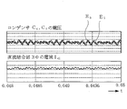
- FIG. 4 is a waveform diagram showing voltages of capacitors on the converter side and the inverter side, and currents in the DC coupling section;
- FIG. 4 is a waveform diagram showing voltages of capacitors on the converter side and the inverter side, and currents in the DC coupling section; 3 is a diagram showing an example of operating waveforms on the converter side of the power conversion system shown in FIG. 2;
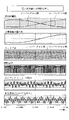
- FIG. 4 is a waveform diagram showing an AC side current, an AC side voltage fundamental wave, a carrier wave, a capacitor voltage, and a DC coupling portion current when carrier waves on the converter side and the inverter side are in phase.
- FIG. 4 is a waveform diagram showing an AC side current, an AC side voltage fundamental wave, a carrier wave, a capacitor voltage, and a DC coupling portion current when the carrier waves on the converter side and the inverter side are in opposite phases;
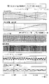
- FIG. 4 is a waveform diagram showing an AC side current, an AC side voltage fundamental wave, a carrier wave, a chopping current, a capacitor voltage, and a DC coupling portion current when the power factors on the converter side and the inverter side are changed.
- FIG. 4 is a waveform diagram showing an AC side current, an AC side voltage fundamental wave, a carrier wave, a chopping current, a capacitor voltage, and a DC coupling portion current when the power factors on the converter side and the inverter side are changed.
- FIG. 4 is a main circuit configuration diagram of a power conversion system according to another embodiment of the present disclosure; FIG.
- FIG. 4 is a waveform chart showing an AC side current, an AC side voltage fundamental wave, a carrier wave, a cutting current, a capacitor voltage, and a DC coupling portion current when both the converter and the inverter are composed of a single power conversion portion; be.
- Waveform diagram showing an AC side current, an AC side voltage fundamental wave, a carrier wave, a cutting current, a capacitor voltage, and a DC coupling portion current when the converter and the inverter are composed of a plurality of power conversion portions connected in parallel. is. Shows the AC side current, AC side voltage fundamental wave, carrier wave, chopping current, capacitor voltage, and DC coupling portion current when both the converter and the inverter consist of a plurality of power conversion portions connected in parallel.
- 1B is a block diagram showing a modification of the control circuit of FIG. 1B;
- FIG. 1 is a configuration diagram when the present disclosure is applied to an aircraft propulsion system;
- FIG. 1A is a main circuit configuration diagram of a power conversion system according to an embodiment of the present disclosure
- FIG. 1B is a block diagram showing an example of its control circuit.
- AC power source G includes a three-phase AC generator that obtains rotational force from an external force such as an engine.
- a three-phase voltage-type converter (hereinafter also simply referred to as a converter) 10 is connected to the AC power supply G, and a three-phase voltage-type inverter ( 20 is connected.
- the DC coupling section 30 is an example of DC coupling means.
- the inverter 20 converts the DC power input through the DC coupling unit 30 into AC power and outputs the AC power to the AC motor M such as a three-phase synchronous motor or an induction motor, and the AC motor M generates a predetermined torque. Drive a load (not shown).
- the converter 10 includes a power converter 11 in which semiconductor switching elements (hereinafter also simply referred to as switching elements) S 1 to S 6 such as IGBTs and FETs are connected in a three-phase bridge connection, and a first power converter 11 connected between its DC output terminals. and a capacitor Cc for voltage smoothing as a capacitor of .
- the inverter 20 includes a voltage-smoothing capacitor C i as a second capacitor connected to the capacitor C c via a DC coupling section 30, and switching elements S 21 to S 26 connected across the two ends of the capacitor C 1 to S 26 in a three-phase bridge connection. and a power conversion unit 21 including
- the converter 10 converts the AC voltage into a DC voltage by turning on/off the switching elements S 1 to S 6 , smoothes it by the capacitor C c , and supplies it to the inverter 20 via the DC coupling section 30 .
- the input DC voltage is smoothed by the capacitor C i , converted to AC voltage by the ON/OFF operation of the switching elements S 21 to S 26 , and supplied to the AC motor M.
- the symbols C c and C i are used for both capacitors and capacitances.
- the inductance of the DC coupling portion 30 is represented by Lci .
- the inductance L ci includes the inductance of the cable itself as the DC coupling portion 30 and the inductance of the DC reactor and the cable when the DC reactor as a component is connected in the middle of the cable.
- a feature of this embodiment is that, as shown in FIG. (hereinafter also referred to as a CLC resonant circuit).
- a feature of this embodiment is that the switching frequencies of the converter 10 and the inverter 20 are equal and set higher than the resonance frequency of the CLC resonance circuit.
- at least one of the converter 10 and the inverter 20 is controlled so that the phases of predetermined components of the voltage pulsations of the capacitors C c and C i generated by the switching of the converter 10 and the inverter 20 are substantially in phase.
- the object is to control the switching operation. This reduces the pulsation of the current Ici of the DC coupling section 30 caused by the difference in voltage pulsation.
- the relationship between the resonant frequency of the CLC resonant circuit and the switching frequencies of converter 10 and inverter 20 will be considered.
- the switching frequency or its harmonic frequency coincides with the resonant frequency
- the oscillating current in the loop consisting of C c , C i , L ci increases without limit, causing an overvoltage on the capacitors C c , C i or an overvoltage in the loop.
- the electric current leads to destruction of the device. Even if such a situation could be avoided, the switching frequency may be lower than the resonance frequency.
- the inductance Lci when viewed from the power conversion unit 11 of the converter 10 or the power conversion unit 21 of the inverter 20, the inductance Lci is higher than the capacitor Cc and the capacitor Ci provided in these DC voltage units at the switching frequency. Impedance will be low. Therefore, most of the pulsating components of the current generated by the switching operation flow through the inductance Lci without being absorbed by the capacitors Cc and Ci . function will be lost.
- setting the switching frequencies of the converter 10 and the inverter 20 (power conversion units 11 and 21) higher than the resonance frequency of the CLC resonance circuit is a requirement for stably operating the system.
- FIG. 2 is a simplified version of FIG. 1A.
- of the impedance Z viewed from the converter 10 side is, for example, as shown in FIG. The same applies to the impedance viewed from the inverter 20 side.
- the impedance Z has two singularities.
- the difference between the voltage pulsations of the capacitors C c and C i due to the switching of the converter 10 and the inverter 20 is applied to the reactance L ci . Ripple of the current flowing through ci can be reduced.
- the power conversion units 11 and 21 of the converter 10 and the inverter 20 apply PWM-controlled voltages to the AC power source G and the AC motor M, respectively, to directly or indirectly control the current.
- the AC power supply G and the AC motor M themselves usually have voltages of a fundamental wave and its harmonics. These voltages are superimposed with rectangular wave voltages by PWM control.
- the current flowing from the AC power supply G to the converter 10 and the current flowing from the AC motor M to the inverter 20 are continuous. These continuous currents are cut by switching the power converters 11 and 21, and pulse-shaped currents (hereinafter referred to as cut currents) flow to the DC circuit side, and the CLC resonance consisting of the capacitors C c and C i and the inductance L ci It becomes the input of the circuit.
- the waveform of this cutting current is substantially determined by the current of the AC power source G and the switching of the power converter 11, and by the current of the AC motor M and the switching of the power converter 21. It behaves like a current source.
- Voltage pulsations of the capacitors C c and C i caused by the switching operations of the power converters 11 and 21 will be further described. As is clear from the description so far, a current pulsation occurs as a result of the difference between the voltage pulsations of the capacitors C c and C i being applied to the inductance L ci . Therefore, by suppressing the difference between the voltage pulsations of the capacitors C c and C i to a small value, the current pulsation in the inductance L ci can be reduced. Voltage pulsations of the capacitors C c and C i caused by switching of the power converters 11 and 21 have components related to the switching frequency.
- the power converters 11 and 21 should be adjusted so that the “predetermined component” among these components has substantially the same phase in the capacitors C c and C i .
- the "predetermined component” means “main frequency component” or “particularly desired to be reduced frequency component” among the frequency components of the voltage pulsation of the capacitors C c and C i , or the voltage amplitude in the time waveform of the voltage pulsation. is the "time component" of the period when is large.
- FIG. 4A and 4B specifically show the above point.
- 4A and 4B show the waveforms of the voltages Ec and Ei of the capacitors Cc and Ci on the converter 10 side and the inverter 20 side, and the current Ici of the DC coupling section 30.
- FIG . FIG. 4B shows a case where Ec and Ei are substantially in phase when c (indicated by a solid line) and Ei (indicated by a dashed line) are substantially in phase. In both cases, the voltages E c and E i pulsate, and the difference between these voltage pulsations is applied to the inductance L ci of the DC coupling section 30 to flow the current I ci .
- the voltage pulsations of Ec and Ei which are generally in opposite phase , have a larger differential voltage as the amplitude of each voltage increases.
- the voltage pulsations of E c and E i are approximately in phase, which reduces the pulsation of the differential voltage applied to the inductance L ci and also reduces the current pulsation of I ci . Therefore, by controlling the switching operations of the converter 10 and the inverter 20 so that the voltage pulsations of E c and E i are substantially in phase as shown in FIG. can be done.
- FIG. 5 is an example of operating waveforms of the power conversion system shown in FIG.
- the voltage E c of C c and the current I ci of the DC coupling 30 are shown.
- the auxiliary line indicates the timing at which the carrier wave reaches the maximum value. From this, it can be seen that the frequency of the voltage pulsation of the capacitor Cc due to the cutting current is governed by the frequency of the carrier wave.
- the voltage pulsation of the capacitor Cc increases during the period when the cutting current pulse exists, and decreases during the period when the cutting current pulse does not exist (when the cutting current is zero). I understand. This can be seen from the cutting current flowing into the capacitor Cc .
- the voltage Ei of the capacitor C i decreases during the period when the cutting current pulse exists, and increases during the period when the pulse does not exist.
- PWM converters and PWM inverters it is common to generate PWM pulses by comparing a carrier wave typified by a triangular wave with a voltage command value.
- the current between the power conversion section of the converter or inverter and the capacitor of the DC voltage section becomes a pulse-shaped chopped current, and the main frequency components of this chopped current are integral multiples of the frequency of the carrier wave. becomes a component of
- the frequency components of the voltage pulsation of the capacitor include a plurality of components among the fundamental frequency component of the carrier wave, its harmonic components, and their sideband wave components.
- the difference between the voltage pulsations of the capacitors C c and C i determines the current pulsation of the DC coupling section 30 .
- In-phase is effective. Therefore, when the PWM pulse to be applied to the converter 10 and the inverter 20 is generated by comparing the voltage command value and the carrier wave, the frequencies of the carrier waves used in the converter 10 and the inverter 20 are made equal, and both capacitors C It is desirable to adjust the phase relationship between the two carrier waves so that the voltage pulsations of c 1 and C i are substantially in phase. If the frequencies of the two carrier waves are not equal, the voltage pulsations of the capacitors C c and C i will be out of phase with time. It becomes impossible to suppress the current pulsation of the coupling portion 30 .
- the voltage command value shown in FIG. 5 described above corresponds to a single-phase voltage fundamental wave on the AC side.
- This voltage command value is compared with the carrier wave to generate a PWM pulse for generating a voltage to be output to the AC sides of converter 10 and inverter 20 .
- the cutting current is zero during the period in which the switching elements of all three phases of the upper arm or the lower arm are on (called the zero-phase period), It becomes a pulse-like waveform equal to the electric current.
- the zero-phase period the cutting current is zero during the period in which the switching elements of all three phases of the upper arm or the lower arm are on
- the voltage command value (fundamental wave) is a three-phase balanced sine wave
- the amplitude of the other two-phase voltage command values (not shown in FIG. 5) at the time when the amplitude of one of the phases reaches its maximum is , the sign of which is reversed at 1/2 of the amplitude of the one phase.
- the zero-phase period is short near the peak of the carrier wave and long near the trough of the carrier wave. That is, adjacent pulses of the cutting current are close to each other near the peak of the carrier wave, and separate adjacent pulses of the cutting current near the valley of the carrier wave.
- Such a phenomenon repeats every time the three-phase voltage command value (voltage fundamental wave) alternately becomes a maximum value and a minimum value.
- the magnitude of the voltage pulsation of the capacitors C c and C i is directly affected by the position of the pulse of the cutting current. That is, if adjacent pulses of the chopping current are close together in the converter 10, the current will flow into the capacitor Cc with high frequency, resulting in a large increase in the voltage across the capacitor Cc . On the other hand, if the adjacent pulses of the cutting current are discrete , no current flows into the capacitor Cc during the zero phase period. Conversely, on the inverter 20 side, the voltage across capacitor C i decreases significantly when adjacent pulses of chopping current are close, and increases significantly when they are separated.
- ⁇ Period A in which the cutting current pulse repeats approaching and discrete, is three times in the half cycle of the three-phase voltage command value (voltage fundamental wave). Between periods A, the cutting current pulse is roughly equal. There is a period B during which it is arranged. - During the period A, the amplitude of the voltage pulsation of the capacitor Cc is large. The voltage of the capacitor Cc on the converter 10 side greatly increases during the period when the chopping current pulses are close to each other, and decreases greatly during the period when the pulses are discrete.
- the magnitude of the voltage pulsation of the capacitors C c and C i is directly affected by the proximity and discontinuity of the pulse of the cutting current, and the proximity and discontinuity of the pulse of the cutting current are affected by PWM control by carrier comparison. This is because it is determined by the phase of the voltage command value.
- the carrier waves used by the converter 10 and the inverter 20 should have the same frequency and opposite phases.
- the increase and decrease in the voltages of the capacitors C c and C i with respect to the approach and the dispersal of the pulse of the cutting current are opposite between the converter 10 and the inverter 20. Therefore, the voltages of the capacitors C c and C i In order to match the increase and decrease, it is sufficient to reverse the approach and the separation of the cutting current pulses.
- FIG. 6 shows this. 6A shows a case where the carrier waves of the converter 10 and the inverter 20 are in phase, and FIG. 6B shows a case where the carrier waves of the converter 10 and the inverter 20 are in opposite phase. Voltages E c , E i across capacitors C c , C i and current I ci in DC coupling 30 are shown. Note that the scale of the graph is common to FIGS. 6A and 6B. In FIGS. 6A and 6B, the waveforms overlap because the AC-side voltage fundamental wave is synchronized between the converter 10 and the inverter 20, and the AC-side current of the inverter 20 is in phase with the voltage fundamental wave, that is, the power factor is 1. is shown.
- the period during which the amplitude of the voltage pulsation of the capacitor is large is the same in the converter 10 and the inverter 20.
- FIG. 6A when the carrier waves are in phase shown in FIG. 6A, the voltages E c and E i are generally opposite in phase, whereas in the case of the carrier waves in opposite phase shown in FIG. 6B, the voltages E c and E i are They are roughly in phase. Therefore, it is clear that the pulsation of the current Ici can be suppressed in the case shown in FIG. 6B compared to the case shown in FIG. 6A.
- any one-phase voltage fundamental wave on the AC side of the converter 10 and the inverter 20 has the same frequency and opposite phase, and the carrier waves of the converter 10 and the inverter 20 have the same frequency and the same phase. Similar effects can also be obtained in this case.
- FIG. 7A shows an alternating current when the power factor angle ⁇ on the converter 10 side is approximately 0° (the power factor is approximately 1) and the power factor angle ⁇ on the inverter 20 side is ⁇ 10° (current lag phase).
- FIG. 4 is a waveform diagram showing a side current, an AC side voltage fundamental wave, a carrier wave, a chopping current, a capacitor voltage, and a DC coupling portion current;
- FIG. 7B shows the AC side current when the power factor angle ⁇ on the converter 10 side is approximately 0° (the power factor is approximately 1) and the power factor angle ⁇ on the inverter 20 side is ⁇ 30° (current lag phase).
- FIG. 4 is a waveform diagram showing a side current, an AC side voltage fundamental wave, a carrier wave, a chopping current, a capacitor voltage, and a DC coupling portion current
- FIG. 7B shows the AC side current when the power factor angle ⁇ on the converter 10 side is approximately 0° (the power factor is approximately 1) and the
- FIG. 3 is a waveform diagram showing an AC side voltage fundamental wave, a carrier wave, a cutting current, a voltage of a capacitor, and a current of a DC coupling portion; Note that the fundamental voltage waves of the converter 10 and the inverter 20 are in phase, and the carrier waves are in opposite phase. In the waveform of the cutting current, the solid line indicates the current on the converter 10 side, and the broken line indicates the current on the inverter 20 side. As described above, even when the current phases of the converter 10 and the inverter 20 are different, the approach and separation of the pulse of the chopping current are determined only by the phase of the voltage fundamental wave without depending on the power factor as described above. Therefore, it can be seen that the repetition of the amplitudes of the voltage pulsations of the capacitors C c and C i is substantially the same in both the converter 10 and the inverter 20, and similar effects can be obtained.
- Example according to the fifth aspect is also applicable when at least one of the converter and the inverter is configured by a plurality of power conversion units in which the DC voltage units are connected in parallel.
- FIG. 8 Another embodiment of the disclosure is shown in FIG. 8, the converter 10A is configured by connecting two power converters 11 and 12 in parallel, and the inverter 20A is configured by connecting two power converters 21 and 22 in parallel.
- One AC power supply G is connected to the converter 10A, and one AC motor M is connected to the inverter 20A.
- the switching frequencies of the power converters 11 and 12 and the power converters 21 and 22 are all the same.
- the power converters 11 and 12 and the power converters 21 and 22 are adjusted so that the predetermined components of the voltage pulsations of the capacitors C c and C i are substantially in phase. , respectively, it is possible to suppress the current pulsation of the DC coupling section 30 .
- the sum of the currents flowing into the capacitor Cc is smoothed, and the voltage pulsation of the capacitor Cc can be suitably suppressed.
- the PWM pulses of each should be made to alternate.
- the method of shifting the PWM pulse of the power converter is the same for the power converters 21 and 22 of the inverter 20A. It goes without saying that this embodiment can contribute to the reduction of current pulsation in the DC coupling section 30 in the same manner as the above-described embodiments.
- the switching frequency component which is the lowest frequency among the current ripple components of the DC coupling unit 30 caused by the switching operations of the converter 10A and the inverter 20A, can be suppressed by controlling the phases of the carrier waves of the converter 10A and the inverter 20A. to reduce the effect of control error.
- the plurality of power conversion units 11 and 12 and the power conversion units 21 and 22 connected in parallel are arranged in physically close positions (for example, in the same housing).
- the phase of the carrier wave can be managed with higher accuracy than between converter 10A and inverter 20A. Therefore, the harmonic components of the switching frequency should be suppressed by the interaction of a plurality of power converters connected in parallel.
- the cable or the like that constitutes the DC coupling section 30 behaves like a distributed constant. This behavior becomes more pronounced, for example, the longer the cable length or the closer the positive and negative conductors are. Distributed constant behavior generally appears more strongly as the frequency increases. Therefore, when a high-frequency voltage fluctuation is applied to both ends of a cable, etc., even if it is attempted to cancel it by controlling the phase at both ends of the cable, the distributed constant element of the cable, specifically, the capacitance between the positive and negative conductors It is conceivable that a high frequency current will flow through the component.
- the harmonic components of the switching frequency at both ends of the cable are canceled by the interaction of the plurality of power converters 11 and 12 and the power converters 21 and 22, respectively. Suppressed by managing the phases at both ends of the cable. As a result, it is possible to suppress the influence of the distribution constant behavior of the cable so that the current pulsation can be preferably suppressed.
- the switching frequency components of the voltage pulsation of the capacitors C c and C i of the converter 10A and the inverter 20A are The pulse generation timings of the DC bus currents of the power converters 11 and 12 and the power converters 21 and 22 may be offset to cancel each other.
- the harmonic components of the switching frequency may be substantially in phase in the converter 10A and the inverter 20A. That is, of the current pulsation generated in the DC coupling unit 30 such as a cable, the switching frequency component, which usually has the highest component ratio, is generated at both ends of the DC coupling unit 30 as a pulse of the DC bus current of the power conversion units 11 and 12.
- Both ends of the DC coupling unit 30 are, for example, the insides of the converter 10A and the inverter 20A.
- the interaction between converter 10A and inverter 20A that is, the predetermined components of the voltage pulsation of capacitors C c and C i are made in phase. It is something that cancels out.
- Example according to Tenth Aspect further embodies the case where the converter 10A and the inverter 20A are configured by a plurality of power converters connected in parallel.
- the same carrier wave is applied to each power conversion unit. and a predetermined phase difference between each carrier wave. This makes it possible to easily shift the generation timing of the cutting current pulse output from each power converter. This can be easily understood from the explanation using FIG.
- the carrier waves given to each power conversion unit are inverted, and when there are three power conversion units, the phase difference between the carrier waves is set to 120° and evenly distributed. It is possible to shift. In either case, the generation timings of the cutting current pulses generated by the plurality of power converters are evenly shifted, so that the voltage pulsation of the capacitors C c and C i and the current pulsation of the DC coupling section 30 can be reduced. Alternatively, it is also effective to shift the phase of the carrier wave so as to cancel out the harmonic components of the switching frequency.
- the frequencies of the carrier waves of the converter 10A and the inverter 20A are made the same, and the carrier wave on the converter 10A side and the carrier wave on the inverter 20A side are By adjusting the phase relationship with the wave, the main components of the voltage pulsations of the capacitors C c and C i can be substantially in phase to suppress the current pulsation of the DC coupling section 30 .
- Example according to the eleventh aspect As shown in FIG. 8, even when the converter 10A and the inverter 20A have a plurality of power conversion units connected in parallel, the frequency of the AC side voltage fundamental wave of the converter 10A and the inverter 20A are made the same, the timing at which the amplitudes of the voltage pulsations of the capacitors C c and C i fluctuate can be matched.
- the cutting currents generated by the power conversion units also have similar waveforms, and these cutting currents have similar waveforms.
- a pulsating current can be favorably canceled by providing a phase difference.
- FIG. 9A and 9B are waveform diagrams showing simulation results of this embodiment.
- FIG. 9A shows, for comparison, the AC side current, the AC side voltage fundamental wave, the carrier wave, the cutting current, the voltage of the capacitor
- FIG. 4 is a waveform diagram showing a current in a DC coupling section;
- the carrier waves on the converter 10 side and the inverter 20 side have opposite phases, which corresponds to the example of FIG. 6B described above.
- FIG. 9B is a waveform diagram of each part when the converter 10A and the inverter 20A have the power converters 11 and 12 and the power converters 21 and 22 connected in parallel, respectively, as shown in FIG. FIG.
- FIG. 9B synchronizes the AC-side voltage fundamental waves of the converter 10A and the inverter 20A, and makes the amplitudes of the AC-side current and AC-side voltage fundamental waves approximately equal for each set of the power conversion units 11 and 21 and the power conversion units 12 and 22. indicates the case. Furthermore, FIG. 9B shows a case where the frequencies of the carrier waves of the four power converters 11, 12, 21, and 22 are made the same and the respective phases are sequentially set to 0°, 90°, 180°, and 270°. That is, in converter 10A, the phases of carrier waves for power converters 11 and 12 are out of phase with each other by 90°, and in inverter 20A, the phases of carrier waves with respect to power converters 21 and 22 are out of phase with each other by 90°.
- FIG. 9B shows only the carrier wave for power conversion unit 11 in converter 10A and the carrier wave for power conversion unit 21 in inverter 20A (the phase difference between them is 180°).
- the carrier wave for is omitted from the drawing.
- the solid line indicates the power conversion unit 11 side in the converter 10A
- the dashed line indicates the power conversion unit 21 side in the inverter 20A
- the solid line indicates the voltage of the capacitors C c and C i .
- the dashed line indicates the voltage E i of the capacitor C i .
- the corresponding waveforms have the same scale.
- the frequency components of the carrier waves which are the main components of the current pulsation of the DC coupling section 30, are in phase and canceled.
- the double frequency components of the carrier waves are in phase with each other and canceled between the power conversion units 11 and 12 in the converter 10A and between the power conversion units 21 and 22 in the inverter 20A.
- FIG. 10 contrary to FIG. 9B, the double frequency component of the carrier wave is canceled between the converter 10A and the inverter 20A, and between the power conversion units 11 and 12 in the converter 10A 2 is a waveform diagram when the frequency components of the carrier wave are canceled between the power converters 21 and 22 of FIG.
- the frequencies of the carrier waves of the four power converters 11, 12, 21, and 22 are the same, and the respective phases are set to 0°, 180°, 90°, and 270° in order.
- FIG. 10 shows only the carrier wave for the power conversion unit 11 in the converter 10A and the carrier wave for the power conversion unit 21 in the inverter 20A (the phase difference between them is 90°).
- the carrier wave for is omitted from the drawing.
- the solid line indicates the power converter 11 side in the converter 10A
- the dashed line indicates the power converter 21 side in the inverter 20A
- the voltages of the capacitors C c and Ci are the voltages of the capacitor C c
- E c the dashed line indicates the voltage E i on the capacitor C i .
- FIG. 10 it can be seen that the current pulsation in the DC coupling section 30 is remarkably reduced as in FIG. 9B.
- the two power converters 21 and 22 on the inverter 20A side are operated in the same way as if they were one power converter, that is, the AC side voltage, the AC side current and the carrier wave are shared. It suppresses current ripple in the DC coupling section 30 .
- This example relates to a control circuit for a power conversion system, and relates to the configuration and operation of the control circuit shown in FIG. 1B described above. A case of controlling the converter 10 and the inverter 20 in FIG. 1A will be described below. A similar control circuit can be applied to Note that the configuration of the control circuit in the present disclosure is not limited to the example of FIG. 1B, as will be described later.
- the power to be sent to the DC coupling section 30 by the converter 10 is the power obtained by adding the shaft output obtained by multiplying the angular velocity to the torque given to the load (not shown) by the inverter 20 via the AC motor M and the loss. is.
- the DC component of the DC voltage section including capacitor Cc of converter 10 should be kept constant. Therefore, the control system of the converter 10 performs feedback control so that the DC voltage of the DC voltage section becomes a predetermined value, and the operation amount becomes the power generation amount P of the AC power supply G.
- This power generation amount P is controlled by causing a current synchronized with the voltage of the AC power supply G to flow.
- the control system of the inverter 20 can manipulate the current. should be operated.
- the converter 10 side performs DC voltage control with a so-called current control minor loop
- the inverter 20 side performs so-called (rotational) speed control with a current control minor loop.
- the frequency of the current of the AC power supply G is given to the inverter 20 as an amount corresponding to the frequency command value of the AC motor M. That is, since the converter 10 controls the current of the AC power supply G, it has information on the frequency of the current of the AC power supply G.
- the inverter 20 side controls the speed of the AC motor M, and the command value for this speed control is directly related to the frequency of the current of the AC motor M.
- This relationship is determined by the type of AC motor M (synchronous motor, induction motor, etc.), the number of poles, and the like. Therefore, in order for the frequency of the current of the AC motor M to match the frequency of the current of the AC power source G, that is, to synchronize the two, information on the frequency of the current held by the converter 10 is sent to the inverter 20 side, and the inverter 20 side generates, for example, a speed command value based on this.
- a specific control method in FIG. 1B is as follows.
- both AC power source G and AC motor M are assumed to be synchronous motors. That is, in the case of a synchronous motor, the frequency of the current and the rotation frequency of the motor are the same as the number of pole pairs (integer) of the motor. Therefore, in both the converter 10 and the inverter 20, the phase angles ⁇ g , ⁇ m of the synchronous motor detected by the position sensors SENS g , SENS m are converted into the electrical angles ⁇ ge , ⁇ by the electrical angle conversion means p g , pe . me , and using these ⁇ ge and ⁇ me , they are given to the rotating coordinate transforming means VR and the inverse transforming means VRI in the control system, respectively. In the case of so-called sensorless control, estimated values calculated using information on voltage and current possessed by the control system are used as ⁇ ge and ⁇ me .
- the alternating currents Ig and Im of the alternating current power source G and the alternating current motor M are converted into direct currents Igd and Igq and Imd and Imq by the rotating coordinate conversion means VR.
- the difference from each current command value is input to the current adjusting means ACR to generate a DC voltage command value.
- These voltage command values are returned to AC voltage commands V c and V i by the inverting means VRI, and compared with carrier waves by the comparators COMP c and COMP i to generate PWM pulses (command values). 21, respectively.
- the phase shift means F can give a predetermined phase difference to the carrier waves of both, if necessary.
- the voltage Ec of the DC voltage section of the converter 10 is detected, and the voltage Ec -lpf passed through the low-pass filter LPF is generated.
- a feedback control system is configured to match the voltage E c - lpf with the target value E cref , and the difference between the two is input to the voltage adjusting means AVR to obtain the power command value.
- a current command value for causing AC power supply G to output a power generation amount corresponding to this is generated by power command value conversion means "P ⁇ I" and given to the current control minor loop on the converter 10 side described above.
- phase synchronization means 43 performs feedback control in order to synchronize the current phase angle .theta.me of the AC motor M with the current phase angle .theta.ge of the AC power supply G as a reference. That is, a value obtained by adding a predetermined offset angle ⁇ adf to the difference between ⁇ ge and ⁇ me is input to the phase adjustment means PLL, and its output is used as the target value ⁇ meref of the rotational frequency of the AC motor M.
- the frequency of the current of the AC motor M is determined according to the load condition of the AC motor M, and the frequency of the current of the AC power source G is matched accordingly. It is also possible to adjust the rotational speed of the rotational power that is the driving source of the AC power supply G so as to match the frequency of the current of the motor M.
- FIG. 11 A block diagram of the control circuit in this case is shown in FIG. In FIG. 11, the phase synchronization means 43A synchronizes the electrical phase angle ⁇ ge of the AC power source G with the electrical phase angle ⁇ me of the AC motor M as a reference .
- the value to which adf is added is input to the phase adjustment means PLL, and its output is used as the target value ⁇ geref of the electrical angular frequency of the AC power supply G. That is, ⁇ geref proportional to the rotation speed of the AC power source G is adjusted so that ⁇ me and ⁇ ge are synchronized. Since the AC power supply G is driven by an external force (not shown), such as an engine, ⁇ geref is given to the external force control system (not shown). Even when this control circuit is used, the fundamental waves of the AC power source G and the AC motor M can be synchronized. In this control system, the target value ⁇ meref of the electrical angular frequency of the AC motor M is given depending on the load.
- the power Pm of the AC motor M is the product of the output torque and the mechanical angular frequency, and the command values for both are known in the control circuit.
- the power Pm of the motor M can be calculated.
- the power required by the AC motor M can be generated by the AC power supply G without delay.
- the AC power supply G must generate power including the losses of the converter 10, the inverter 20, and the AC motor M.
- the effect on the control circuit is small, and , there is no problem because the difference due to these losses is compensated by the feedback control system.
- the inverter 20 tries to obtain power from the converter 10 that exceeds the amount of power generated at that time.
- the voltage of the voltage section drops, and the DC voltage control system of converter 10 operates to increase the amount of power generated.
- the operation is premised on fluctuations in the voltage of the DC voltage section. Therefore, by performing feedforward control of the power Pm, the voltage fluctuation of the DC voltage section as described above can be minimized, so that the power supply is stabilized, and the AC power source G and the AC motor M are basically connected. Synchronization of waves becomes stable and realizable.
- the current pulsation of the DC coupling portion 30 such as a cable is the voltage fundamental wave, the current fundamental wave, and the carrier wave on the AC side of the converter 10 and the inverter 20. Varies depending on wave conditions. Basically, it is effective to match the frequencies of the voltage fundamental wave, the current fundamental wave, and the carrier wave on the AC side between the converter 10 side and the inverter 20 side, and furthermore, the phases of the carrier waves are adjusted. Since it is possible to reduce the current pulsation of the DC coupling section 30 by means of the above, a control system that automatically adjusts these may be constructed.
- the time constant of the automatic adjustment should be larger than the response time constant when driving the AC motor M, for example, about 5 times or more. good.
- the calculation load of the control circuit can be reduced in addition to stably operating the system.
- Example according to 17th aspect There are various fields of application of the power conversion system according to the present disclosure. An example will be described.
- EN1 and EN2 are aircraft jet engines, to which generators G1 and G2 are coupled.
- Converters CON1 and CON2 are connected to generators G1 and G2, and inverters INV1 and INV2 for driving motors M1 and M2 are connected via converters CON1a and CON2a for charging and discharging batteries BAT1 and BAT2.
- the motors M1 and M2 constitute electric fans for propelling the aircraft.
Landscapes
- Engineering & Computer Science (AREA)
- Power Engineering (AREA)
- Life Sciences & Earth Sciences (AREA)
- Sustainable Development (AREA)
- Sustainable Energy (AREA)
- Transportation (AREA)
- Mechanical Engineering (AREA)
- Inverter Devices (AREA)
- Rectifiers (AREA)
- Power Conversion In General (AREA)
Abstract
コンバータ10とインバータ20とがインダクタンス成分を有する直流結合部30により接続された電力変換システムであって、PWM制御されるコンバータ10及びインバータ20のスイッチング周波数を等しくすると共に、そのスイッチング周波数を、第1のコンデンサCcと第2のコンデンサCiとケーブル等の直流結合部30とを含む共振回路の共振周波数よりも高くし、コンバータ10及びインバータ20のスイッチング動作に起因するコンデンサCc,Ciの電圧脈動の所定成分の位相が概ね同相となるように、コンバータ10及びインバータ20の少なくとも一方のスイッチング動作を制御する。
Description
本開示は、PWM(パルス幅変調)制御されるコンバータ及びインバータにより交流/直流/交流変換を行って交流モータを駆動する電力変換システムに関し、詳しくは、コンバータとインバータとの間の直流回路に流れる電流の脈動を低減するための技術に関するものである。
この種の電力変換システムは従来から種々提供されている。しかし、コンバータ及びインバータをそれぞれPWM制御するためのキャリア波の周波数が異なると、コンバータ-インバータ間の直流回路のコンデンサ(電圧型システムの場合)やリアクトル(電流型システムの場合)を流れる電流の脈動が大きくなって制御が不安定化する。この場合、コンデンサやリアクトルに要求される容量が大きくなることが知られている。
そこで、例えば特許文献1には、コンバータ側のキャリア波とインバータ側のキャリア波とを、同一の波形または反転させた波形とし、あるいは、同一周波数で所定の位相差を持たせた波形として、直流回路の電流の脈動を低減することが記載されている。
また、特許文献2には、コンバータ-インバータ間の直流回路に流れる共振電流を抑制するために、コンバータ及びインバータのキャリア波の周波数及び位相を同期させ、上記直流回路には、二つのキャリア波の位相差がゼロの時に共振電流が少なくなるように直流コンデンサ等を付加することが記載されている。
また、特許文献2には、コンバータ-インバータ間の直流回路に流れる共振電流を抑制するために、コンバータ及びインバータのキャリア波の周波数及び位相を同期させ、上記直流回路には、二つのキャリア波の位相差がゼロの時に共振電流が少なくなるように直流コンデンサ等を付加することが記載されている。
なお、特許文献3には、直流送電線を介して接続されるコンバータ及びインバータの直流電圧部に電圧平滑用のコンデンサをそれぞれ備えた直流送電システムが開示されている。ここで、前記コンデンサは、コンバータ及びインバータのスイッチングに起因する直流電圧のサージを抑制して素子の過電圧破壊を防止すると共に、交流電源や負荷電力の変動時に直流電圧を安定化させる作用を果たしている。
特許文献1には、特許文献3のように直流電圧部にコンデンサを備えたコンバータ及びインバータが直流回路によって接続されるシステムが開示されていない。
また、特許文献2に係る従来技術では、直流回路のインピーダンスや二つの電力系統の条件、コンバータ及びインバータの電圧、電流等によって決まる共振電流が少なくなるようにシミュレーションを行って直流回路を構成している。しかし、この直流回路の共振電流を抑制する原理が具体的に示されておらず、直流回路に接続されるコンデンサやリアクトル等の接続構成や作用も明確には開示されていない。
更に、特許文献3に係る従来技術は、コンバータ及びインバータの制御回路にアクティブフィルタ機能を持たせることで交流電源系統に流出する低次高調波を抑制する発明であり、直流回路の電流の脈動を低減することを課題とするものではない。
また、特許文献2に係る従来技術では、直流回路のインピーダンスや二つの電力系統の条件、コンバータ及びインバータの電圧、電流等によって決まる共振電流が少なくなるようにシミュレーションを行って直流回路を構成している。しかし、この直流回路の共振電流を抑制する原理が具体的に示されておらず、直流回路に接続されるコンデンサやリアクトル等の接続構成や作用も明確には開示されていない。
更に、特許文献3に係る従来技術は、コンバータ及びインバータの制御回路にアクティブフィルタ機能を持たせることで交流電源系統に流出する低次高調波を抑制する発明であり、直流回路の電流の脈動を低減することを課題とするものではない。
本開示の解決課題は、コンバータとインバータとの間の直流回路(直流結合手段の一例)と、コンバータ及びインバータの直流電圧部にそれぞれ接続されたコンデンサとによって構成された共振回路を有し、直流回路を流れる電流の脈動を低減可能とした電力変換システムを提供することにある。
本開示は、以下の態様に関する。第1態様は、
電力変換システムであって、
交流電源と、
前記交流電源の交流電力をPWM制御により直流電力に変換するコンバータと、
前記コンバータから出力される直流電力をPWM制御により交流電力に変換して交流モータに供給するインバータと、
前記コンバータの直流電圧部に接続された第1のコンデンサと、
前記インバータの直流電圧部に接続された第2のコンデンサと、
前記第1のコンデンサと前記第2のコンデンサとを接続し、インダクタンス成分を有する直流結合部と、を備え、
前記コンバータ及び前記インバータのスイッチング周波数を等しくすると共に、当該スイッチング周波数を、前記第1のコンデンサと前記第2のコンデンサと前記直流結合部とを含む共振回路の共振周波数よりも高くし、
前記コンバータ及び前記インバータのスイッチング動作によって生じる前記第1のコンデンサ及び前記第2のコンデンサの電圧脈動の所定成分の位相が概ね同相となるように、前記コンバータ及び前記インバータの少なくとも一方のスイッチング動作を制御することを特徴とする。
電力変換システムであって、
交流電源と、
前記交流電源の交流電力をPWM制御により直流電力に変換するコンバータと、
前記コンバータから出力される直流電力をPWM制御により交流電力に変換して交流モータに供給するインバータと、
前記コンバータの直流電圧部に接続された第1のコンデンサと、
前記インバータの直流電圧部に接続された第2のコンデンサと、
前記第1のコンデンサと前記第2のコンデンサとを接続し、インダクタンス成分を有する直流結合部と、を備え、
前記コンバータ及び前記インバータのスイッチング周波数を等しくすると共に、当該スイッチング周波数を、前記第1のコンデンサと前記第2のコンデンサと前記直流結合部とを含む共振回路の共振周波数よりも高くし、
前記コンバータ及び前記インバータのスイッチング動作によって生じる前記第1のコンデンサ及び前記第2のコンデンサの電圧脈動の所定成分の位相が概ね同相となるように、前記コンバータ及び前記インバータの少なくとも一方のスイッチング動作を制御することを特徴とする。
第2態様は、第1態様に記載した電力変換システムであって、前記コンバータ及び前記インバータにそれぞれ与えるPWMパルスを電圧指令値とキャリア波との比較により生成し、前記コンバータ側及び前記インバータ側のキャリア波を同一周波数とし、かつ両キャリア波の間に所定の位相関係を持たせることを特徴とする。
第3態様は、第2態様に記載した電力変換システムであって、前記交流電源及び前記交流モータの相数を等しくし、前記交流電源及び前記交流モータにおける一相の電圧の基本波が同一周波数であって概ね同相となるように前記コンバータ及び前記インバータの少なくとも一方を制御すると共に、前記コンバータ側及び前記インバータ側のキャリア波の位相を互いに反転させたことを特徴とする。
第4態様は、第2態様に記載した電力変換システムであって、前記交流電源及び前記交流モータの相数を等しくし、前記交流電源及び前記交流モータにおける一相の電圧の基本波が同一周波数であって概ね逆相となるように前記コンバータ及び前記インバータの少なくとも一方を制御すると共に、前記コンバータ側及び前記インバータ側のキャリア波の位相を同相としたことを特徴とする。
第5態様は、第1態様から第4態様のいずれか一つの態様に記載した電力変換システムであって、前記コンバータ及び前記インバータの少なくとも一方が、直流電圧部が並列接続された複数の電力変換部を有することを特徴とする。
第6態様は、第5態様に記載した電力変換システムであって、前記複数の電力変換部のスイッチング周波数を同一にし、かつ、前記コンバータまたは前記インバータを構成する前記複数の電力変換部の直流母線電流のパルス発生のタイミングをずらしたことを特徴とする。
第7態様は、第6態様に記載した電力変換システムであって、前記複数の電力変換部の直流母線電流のパルス発生のタイミングを概ね均等に散在させることを特徴とする。
第8態様は、第6態様に記載した電力変換システムであって、前記第1のコンデンサまたは前記第2のコンデンサの電圧脈動のうち、スイッチング周波数成分については、前記コンバータ及び前記インバータにおいて概ね同相とし、スイッチング周波数の高調波成分については、前記複数の電力変換部の直流母線電流のパルス発生のタイミングをずらすことにより、それぞれ相殺することを特徴とする。
第9態様は、第6態様に記載した電力変換システムであって、前記第1のコンデンサまたは前記第2のコンデンサの電圧脈動のうち、スイッチング周波数成分については、前記複数の電力変換部の直流母線電流のパルス発生のタイミングをずらし、スイッチング周波数の高調波成分については、前記コンバータ及び前記インバータにおいて概ね同相とすることにより、それぞれ相殺することを特徴とする。
第10態様は、第6態様から第9態様のいずれか一つの態様に記載した電力変換システムであって、前記複数の電力変換部にそれぞれ与えるPWMパルスを電圧指令値とキャリア波との比較により生成し、これらのキャリア波を同一周波数として各キャリア波の間に所定の位相関係を持たせると共に、前記コンバータ及び前記インバータに用いるキャリア波を同一周波数とし、かつこれらのキャリア波の間に所定の位相関係を持たせたことを特徴とする。
第11態様は、第10態様に記載した電力変換システムであって、前記交流電源及び前記交流モータの相数を等しくすると共に交流側電圧の基本波の周波数を同一にし、前記コンバータ及び前記インバータにおいて、前記複数の電力変換部の交流側電圧及び交流側電流の基本波の振幅を概ね等しくすることを特徴とする。
第12態様は、第5態様から第11態様のいずれか一つの態様に記載した電力変換システムであって、前記複数の電力変換部の一部を停止させるときには、スイッチングに起因する前記第1のコンデンサまたは前記第2のコンデンサの電圧脈動の所定成分の位相が前記コンバータ及び前記インバータにおいて概ね同相になるように制御することを特徴とする。
第13態様は、第1態様から第12態様のいずれか一つの態様に記載した電力変換システムであって、前記交流電源が外力によって駆動される交流発電機であり、前記コンバータまたは前記インバータの直流電圧平均値が所定値となるように、前記交流発電機の電流を前記コンバータにより制御し、前記交流発電機の電流の周波数を前記交流モータの周波数指令に相当する量として前記インバータに与えることを特徴とする。
第14態様は、第1態様から第12態様のいずれか一つの態様に記載した電力変換システムであって、前記交流電源が外力によって駆動される交流発電機であり、前記コンバータまたは前記インバータの直流電圧平均値が所定値となるように、前記交流発電機の電流を前記コンバータにより制御し、前記交流モータの電流の周波数を前記交流発電機の周波数指令に相当する量として前記外力の制御装置に与えることを特徴とする。
第15態様は、第13態様または第14態様に記載した電力変換システムであって、前記インバータの出力電力に相当する量を、前記コンバータの入力電力指令値に相当する量に加算することを特徴とする。
第16態様は、第1態様から第15態様のいずれか一つの態様に記載した電力変換システムであって、前記直流結合部に流れる電流脈動を低減するように、前記コンバータ及び前記インバータをそれぞれPWM制御するためのキャリア波相互の位相関係、または、前記コンバータ及び前記インバータの交流側電圧基本波相互の位相関係もしくは交流側電流基本波相互の位相関係のうち、少なくとも一つを調整することを特徴とする。
第17態様は、第1態様から第16態様のいずれか一つの態様に記載した電力変換システムが、航空機を推進させる電動ファンの前記交流モータを駆動するシステムであることを特徴とする。
本開示の一態様によれば、新たな素子や部品を追加せずに、コンバータとインバータとの間の直流結合部を流れる電流の脈動を低減し、脈動電流による発生損失を減少させると共に制御を安定化することができる。また、直流電圧部のコンデンサが脈動電流を低減する責務を軽減することにより、コンデンサの静電容量を低減して装置の小型化、低コスト化も可能になる。
以下、図に沿って本開示の実施形態を説明する。
図1Aは、本開示の一実施形態に係る電力変換システムの主回路構成図であり、図1Bはその制御回路の一例を示すブロック図である。
図1Aは、本開示の一実施形態に係る電力変換システムの主回路構成図であり、図1Bはその制御回路の一例を示すブロック図である。
図1Aにおいて、交流電源Gは、例えばエンジン等の外力によって回転力を得る三相の交流発電機を含む。交流電源Gには、三相の電圧型コンバータ(以下、単にコンバータともいう)10が接続され、コンバータ10の直流側には、ケーブル等の直流結合部30を介して三相の電圧型インバータ(以下、単にインバータともいう)20が接続されている。直流結合部30は、直流結合手段の一例である。インバータ20は、直流結合部30を介して入力された直流電力を交流電力に変換して三相同期モータや誘導モータ等の交流モータMに出力し、交流モータMは所定のトルクを発生して負荷(図示せず)を駆動する。
コンバータ10は、IGBTやFET等の半導体スイッチング素子(以下、単にスイッチング素子ともいう)S1~S6が三相ブリッジ接続された電力変換部11と、その直流出力端子間に接続された第1のコンデンサとしての電圧平滑用のコンデンサCcとを備えている。インバータ20は、前記コンデンサCcに直流結合部30を介して接続された第2のコンデンサとしての電圧平滑用のコンデンサCiと、その両端に三相ブリッジ接続されたスイッチング素子S21~S26を含む電力変換部21とを備えている。
コンバータ10は、IGBTやFET等の半導体スイッチング素子(以下、単にスイッチング素子ともいう)S1~S6が三相ブリッジ接続された電力変換部11と、その直流出力端子間に接続された第1のコンデンサとしての電圧平滑用のコンデンサCcとを備えている。インバータ20は、前記コンデンサCcに直流結合部30を介して接続された第2のコンデンサとしての電圧平滑用のコンデンサCiと、その両端に三相ブリッジ接続されたスイッチング素子S21~S26を含む電力変換部21とを備えている。
上記構成において、コンバータ10は交流電圧をスイッチング素子S1~S6のオン・オフ動作により直流電圧に変換してコンデンサCcにより平滑し、直流結合部30を介してインバータ20に供給する。インバータ20では、入力された直流電圧をコンデンサCiにより平滑し、スイッチング素子S21~S26のオン・オフ動作により交流電圧に変換して交流モータMに供給する。
以下では、符号Cc,Ciをコンデンサ及びキャパシタンスの両方の意味で使用する。また、直流結合部30が有するインダクタンスをLciにより表すものとする。なお、このインダクタンスLciは、直流結合部30としてのケーブル自体のインダクタンスや、ケーブルの途中に部品としての直流リアクトルが接続されている場合の、直流リアクトル及びケーブルのインダクタンスを含む。
以下では、符号Cc,Ciをコンデンサ及びキャパシタンスの両方の意味で使用する。また、直流結合部30が有するインダクタンスをLciにより表すものとする。なお、このインダクタンスLciは、直流結合部30としてのケーブル自体のインダクタンスや、ケーブルの途中に部品としての直流リアクトルが接続されている場合の、直流リアクトル及びケーブルのインダクタンスを含む。
(1)第1態様に係る実施例
この実施例の特徴は、図1Aのように、コンバータ10とインバータ20との間の直流回路にコンデンサCc,CiとインダクタンスLciとを含む共振回路(以下、CLC共振回路ともいう)を有する電力変換システムにある。そして、この実施例の特徴は、コンバータ10及びインバータ20のスイッチング周波数を等しくし、かつ、このスイッチング周波数をCLC共振回路の共振周波数よりも高く設定することにある。更に、この実施例の特徴は、コンバータ10及びインバータ20のスイッチングにより発生するコンデンサCc,Ciの電圧脈動の所定成分の位相が概ね同相となるように、コンバータ10及びインバータ20の少なくとも一方のスイッチング動作を制御することにある。これによって、前記電圧脈動の差分に起因する直流結合部30の電流Iciの脈動が低減する。
この実施例の特徴は、図1Aのように、コンバータ10とインバータ20との間の直流回路にコンデンサCc,CiとインダクタンスLciとを含む共振回路(以下、CLC共振回路ともいう)を有する電力変換システムにある。そして、この実施例の特徴は、コンバータ10及びインバータ20のスイッチング周波数を等しくし、かつ、このスイッチング周波数をCLC共振回路の共振周波数よりも高く設定することにある。更に、この実施例の特徴は、コンバータ10及びインバータ20のスイッチングにより発生するコンデンサCc,Ciの電圧脈動の所定成分の位相が概ね同相となるように、コンバータ10及びインバータ20の少なくとも一方のスイッチング動作を制御することにある。これによって、前記電圧脈動の差分に起因する直流結合部30の電流Iciの脈動が低減する。
始めに、CLC共振回路の共振周波数と、コンバータ10及びインバータ20のスイッチング周波数との関係について考察する。
上記スイッチング周波数またはその高調波の周波数が共振周波数に一致すると、Cc,Ci,Lciからなるループにおける振動電流が制限なく増大し、コンデンサCc,Ciの過電圧、あるいは上記ループの過電流によって装置の破壊に至る。仮にこのような事態を回避できたとしても、スイッチング周波数が共振周波数より低い場合がある。この場合、コンバータ10の電力変換部11またはインバータ20の電力変換部21から見て、これらの直流電圧部に設けられたコンデンサCcやコンデンサCiよりもインダクタンスLciの方が、スイッチング周波数におけるインピーダンスが低いことになる。このため、スイッチング動作により発生する電流の脈動成分の多くがコンデンサCc,Ciによって吸収されずにインダクタンスLciに流れることになり、コンデンサCc,Ciが本来担うべき電圧平滑要素としての機能が損なわれてしまう。
以上のことから、コンバータ10及びインバータ20(電力変換部11,21)のスイッチング周波数をCLC共振回路の共振周波数よりも高くすることが、システムを安定的に動作させるための要件となる。
上記スイッチング周波数またはその高調波の周波数が共振周波数に一致すると、Cc,Ci,Lciからなるループにおける振動電流が制限なく増大し、コンデンサCc,Ciの過電圧、あるいは上記ループの過電流によって装置の破壊に至る。仮にこのような事態を回避できたとしても、スイッチング周波数が共振周波数より低い場合がある。この場合、コンバータ10の電力変換部11またはインバータ20の電力変換部21から見て、これらの直流電圧部に設けられたコンデンサCcやコンデンサCiよりもインダクタンスLciの方が、スイッチング周波数におけるインピーダンスが低いことになる。このため、スイッチング動作により発生する電流の脈動成分の多くがコンデンサCc,Ciによって吸収されずにインダクタンスLciに流れることになり、コンデンサCc,Ciが本来担うべき電圧平滑要素としての機能が損なわれてしまう。
以上のことから、コンバータ10及びインバータ20(電力変換部11,21)のスイッチング周波数をCLC共振回路の共振周波数よりも高くすることが、システムを安定的に動作させるための要件となる。
上記の点を、図2,図3を用いて更に説明する。
図2は、図1Aを簡略化したものである。この図2において、コンバータ10側から見たインピーダンスZの絶対値|Z|の周波数特性は、例えば図3のようになり、これを定式化すると数式1が得られる。なお、インバータ20側から見たインピーダンスも同様であり、数式1の右辺において第二分数項の分子のCiがCcになる。
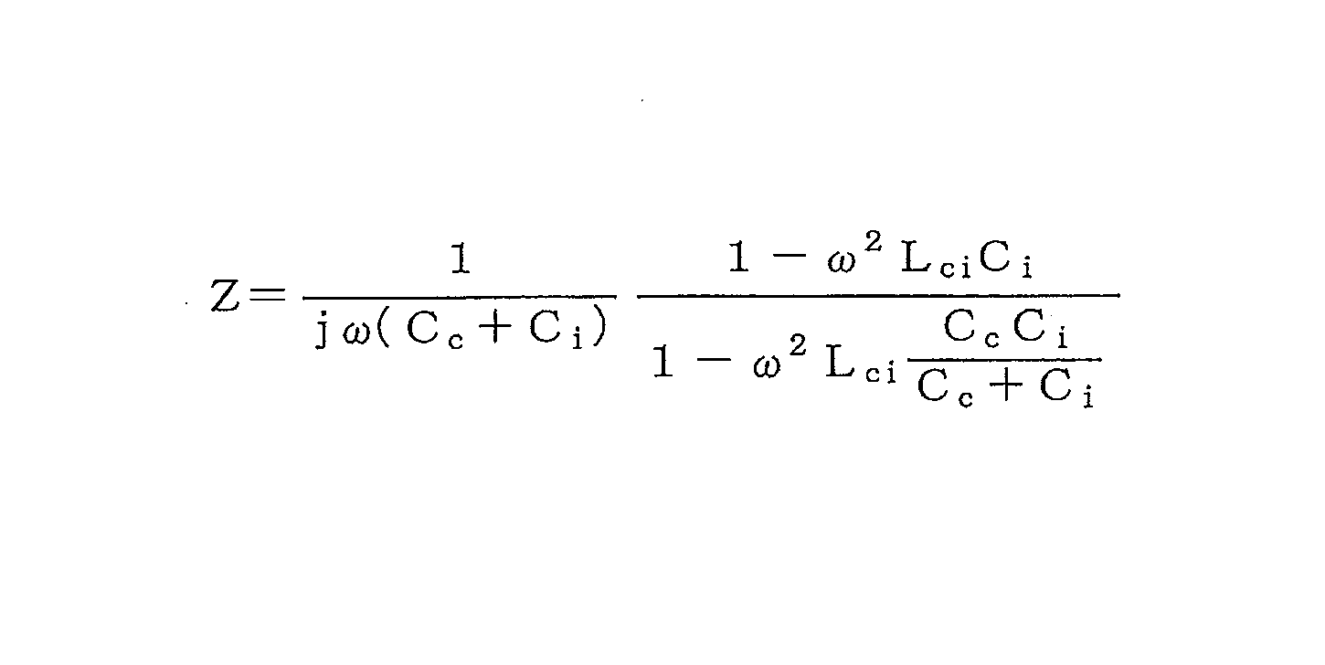
図2は、図1Aを簡略化したものである。この図2において、コンバータ10側から見たインピーダンスZの絶対値|Z|の周波数特性は、例えば図3のようになり、これを定式化すると数式1が得られる。なお、インバータ20側から見たインピーダンスも同様であり、数式1の右辺において第二分数項の分子のCiがCcになる。
数式1から、インピーダンスZには2つの特異点がある。各特異点の周波数は、|Z|がゼロとなる周波数fr1(ω=ωr1=2πfr1)と、|Z|が無限大となる周波数fr2(ω=ωr2=2πfr2)であり、それぞれ数式2、数式3によって与えられる。


ここで、図3では、特異点において|Z|が有限値となっているが、これは実際の回路における抵抗成分を考慮したものであって本質的な問題ではない。また、この抵抗成分は、一般に、Lci,Cc,Ciに対しての影響が小さいので、定式化においては無視されている。
数式2,数式3によれば、必ずfr1<fr2の関係があるため、コンバータ10及びインバータ20のスイッチング周波数は、図3のfr2よりも高くする必要がある。つまり、スイッチング周波数がfr1またはfr2に一致すると共振状態となって過電圧や過電流となり、fr2より低いと、インダクタンスLciにはスイッチング動作に起因する電流成分の多くが流れてしまう。なお、システムを安定的に動作させるためには、コンバータ10及びインバータ20のスイッチング周波数がfr2に近いと共振に近い状態になるため、実用的には、スイッチング周波数をfr2の概ね2倍以上とすることが望ましい。
数式2,数式3によれば、必ずfr1<fr2の関係があるため、コンバータ10及びインバータ20のスイッチング周波数は、図3のfr2よりも高くする必要がある。つまり、スイッチング周波数がfr1またはfr2に一致すると共振状態となって過電圧や過電流となり、fr2より低いと、インダクタンスLciにはスイッチング動作に起因する電流成分の多くが流れてしまう。なお、システムを安定的に動作させるためには、コンバータ10及びインバータ20のスイッチング周波数がfr2に近いと共振に近い状態になるため、実用的には、スイッチング周波数をfr2の概ね2倍以上とすることが望ましい。
次に、図2から明らかなように、コンバータ10及びインバータ20のスイッチングによるコンデンサCc,Ciの電圧脈動の差分はリアクタンスLciに印加されるため、この差分を抑制することで、リアクタンスLciに流れる電流の脈動を低減することができる。
前述した図2において、コンバータ10及びインバータ20の電力変換部11,21は、それぞれ交流電源G及び交流モータMに、PWM制御された電圧を印加して電流を直接または間接的に制御している。交流電源Gや交流モータM自体は、通常、基本波とその高調波の電圧を有している。これらの電圧に、PWM制御による矩形波状の電圧が重畳される。これにより、両者の電圧の差分が、交流電源Gと交流モータMとの間に接続されたリアクトル等に印加されることで電流が平滑化される。但し、上記リアクトル等は、交流電源Gや交流モータMが有するインダクタンス成分によって代用されることが多いため、図2では、その前提でリアクトル等の記載を省略し、直流結合部30が有するインダクタンスLciのみを表記してある。
前述した図2において、コンバータ10及びインバータ20の電力変換部11,21は、それぞれ交流電源G及び交流モータMに、PWM制御された電圧を印加して電流を直接または間接的に制御している。交流電源Gや交流モータM自体は、通常、基本波とその高調波の電圧を有している。これらの電圧に、PWM制御による矩形波状の電圧が重畳される。これにより、両者の電圧の差分が、交流電源Gと交流モータMとの間に接続されたリアクトル等に印加されることで電流が平滑化される。但し、上記リアクトル等は、交流電源Gや交流モータMが有するインダクタンス成分によって代用されることが多いため、図2では、その前提でリアクトル等の記載を省略し、直流結合部30が有するインダクタンスLciのみを表記してある。
上記のように、交流電源Gからコンバータ10に流れる電流や交流モータMからインバータ20に流れる電流は連続的である。これらの連続的な電流を電力変換部11,21のスイッチングにより裁断したパルス状の電流(以下、裁断電流という)が直流回路側に流れ、コンデンサCc,Ci及びインダクタンスLciからなるCLC共振回路の入力になる。この裁断電流の波形は、実質的には、交流電源Gの電流と電力変換部11のスイッチングとによって、並びに、交流モータMの電流と電力変換部21のスイッチングとによって決まるため、CLC共振回路に対しては電流源のような振る舞いをする。
更に、電力変換部11,21のスイッチング周波数を、それぞれから見たCLC共振回路の共振周波数fr2よりも高くした場合、裁断電流の大部分は、電力変換部11からはコンデンサCcに流入し、電力変換部21からはコンデンサCiに流入する。その結果として、コンデンサCc,Ciには、所定の直流電圧に脈動電圧が重畳されることになる。また、裁断電流が有する直流成分は、コンデンサCc,Ciを通らないため、直流結合部30のインダクタンスLciを通ってコンバータ10とインバータ20との間でやりとりされる。これによって、交流モータMが必要とする電力は交流電源Gから供給され、逆に、回生動作によって交流モータMから交流電源Gに向けて電力が供給されることになる。
電力変換部11,21のスイッチング動作によって生じるコンデンサCc,Ciの電圧脈動について、更に説明する。
ここまでの説明から明らかなように、コンデンサCc,Ciの電圧脈動の差分がインダクタンスLciに印加される結果、電流脈動が発生する。そのため、コンデンサCc,Ciの電圧脈動の差分を小さく抑えれば、インダクタンスLciにおける電流脈動を低減することができる。
電力変換部11,21のスイッチングに起因するコンデンサCc,Ciの電圧脈動は、スイッチング周波数に関わる成分を有している。そのため、コンデンサCc,Ciの電圧脈動の差分を小さく抑えるには、この成分のうち「所定成分」について、コンデンサCcとコンデンサCiとにおいて概ね同相となるように電力変換部11,21のスイッチング動作を制御すればよい。この場合の「所定成分」とは、コンデンサCc,Ciの電圧脈動が有する周波数成分のうち「主要な周波数成分」や「特に低減したい周波数成分」、あるいは、電圧脈動の時間波形において電圧振幅が大きい期間の「時間成分」を言う。
ここまでの説明から明らかなように、コンデンサCc,Ciの電圧脈動の差分がインダクタンスLciに印加される結果、電流脈動が発生する。そのため、コンデンサCc,Ciの電圧脈動の差分を小さく抑えれば、インダクタンスLciにおける電流脈動を低減することができる。
電力変換部11,21のスイッチングに起因するコンデンサCc,Ciの電圧脈動は、スイッチング周波数に関わる成分を有している。そのため、コンデンサCc,Ciの電圧脈動の差分を小さく抑えるには、この成分のうち「所定成分」について、コンデンサCcとコンデンサCiとにおいて概ね同相となるように電力変換部11,21のスイッチング動作を制御すればよい。この場合の「所定成分」とは、コンデンサCc,Ciの電圧脈動が有する周波数成分のうち「主要な周波数成分」や「特に低減したい周波数成分」、あるいは、電圧脈動の時間波形において電圧振幅が大きい期間の「時間成分」を言う。
上記の点を具体的に示したのが図4A及び図4Bである。
図4A及び図4Bは、コンバータ10側及びインバータ20側のコンデンサCc,Ciの電圧Ec,Ei、並びに、直流結合部30の電流Iciの波形を示しており、図4AはEc(実線にて示す),Ei(破線にて示す)が概ね逆相の場合、図4BはEc,Eiが概ね同相の場合である。何れの場合も電圧Ec,Eiは脈動しており、これらの電圧脈動の差分が直流結合部30のインダクタンスLciに印加されて電流Iciが流れる。
図4A及び図4Bは、コンバータ10側及びインバータ20側のコンデンサCc,Ciの電圧Ec,Ei、並びに、直流結合部30の電流Iciの波形を示しており、図4AはEc(実線にて示す),Ei(破線にて示す)が概ね逆相の場合、図4BはEc,Eiが概ね同相の場合である。何れの場合も電圧Ec,Eiは脈動しており、これらの電圧脈動の差分が直流結合部30のインダクタンスLciに印加されて電流Iciが流れる。
図4Aにおいて、概ね逆相であるEc,Eiの電圧脈動は、各電圧の振幅が大きいほど差電圧も大きくなるため、この期間にインダクタンスLciを流れるIciには大きな電流脈動が含まれている。一方、図4Bでは、Ec,Eiの電圧脈動は概ね同相であるため、これによってインダクタンスLciに印加される差電圧の脈動が小さくなり、Iciの電流脈動も小さくなる。
従って、図4BのようにEc,Eiの電圧脈動が概ね同相となるようにコンバータ10及びインバータ20のスイッチング動作を制御すれば、直流結合部30を流れる電流Iciの脈動を抑制することができる。
従って、図4BのようにEc,Eiの電圧脈動が概ね同相となるようにコンバータ10及びインバータ20のスイッチング動作を制御すれば、直流結合部30を流れる電流Iciの脈動を抑制することができる。
(2)第2態様に係る実施例
図5は、図2に示した電力変換システムの動作波形の一例であり、上からキャリア波(三角波)及び電圧指令値、裁断電流、コンバータ10側のコンデンサCcの電圧Ec、直流結合部30の電流Iciを示している。
図5の裁断電流については、キャリア波が極大値となるタイミングを補助線で示してある。ここから、裁断電流によるコンデンサCcの電圧脈動の周波数はキャリア波の周波数に支配されることが分かる。また、コンデンサCcの電圧脈動は、詳しく見ると、裁断電流のパルスが存在する期間に増加し、裁断電流のパルスが存在しない期間(裁断電流がゼロの期間)には減少していることが分かる。これは、裁断電流がコンデンサCcに流入していることから理解できる。なお、図示されていないインバータ20側において、コンデンサCiの電圧Eiは、裁断電流のパルスが存在する期間に減少し、パルスが存在しない期間では増加する。
図5は、図2に示した電力変換システムの動作波形の一例であり、上からキャリア波(三角波)及び電圧指令値、裁断電流、コンバータ10側のコンデンサCcの電圧Ec、直流結合部30の電流Iciを示している。
図5の裁断電流については、キャリア波が極大値となるタイミングを補助線で示してある。ここから、裁断電流によるコンデンサCcの電圧脈動の周波数はキャリア波の周波数に支配されることが分かる。また、コンデンサCcの電圧脈動は、詳しく見ると、裁断電流のパルスが存在する期間に増加し、裁断電流のパルスが存在しない期間(裁断電流がゼロの期間)には減少していることが分かる。これは、裁断電流がコンデンサCcに流入していることから理解できる。なお、図示されていないインバータ20側において、コンデンサCiの電圧Eiは、裁断電流のパルスが存在する期間に減少し、パルスが存在しない期間では増加する。
PWMコンバータやPWMインバータにおいては、三角波に代表されるキャリア波と電圧指令値との比較によってPWMパルスを生成することが一般的である。その場合、周知のように、コンバータやインバータの電力変換部と直流電圧部のコンデンサとの間の電流はパルス状の裁断電流となり、この裁断電流の主要な周波数成分はキャリア波の周波数の整数倍の成分となる。これに伴い、コンデンサの電圧脈動の周波数成分は、キャリア波の基本周波数成分とその高調波成分、及び、それらの側帯波の成分のうち複数の成分を含む。
よって、前述したように、コンデンサCc,Ciの電圧脈動の差分によって直流結合部30の電流脈動が決まり、この電流脈動を低減するためには両コンデンサCc,Ciの電圧脈動を概ね同相にすることが有効である。このことから、コンバータ10及びインバータ20に与えるPWMパルスを電圧指令値とキャリア波との比較によって生成する場合には、コンバータ10及びインバータ20に用いるキャリア波の周波数を等しくし、かつ、両コンデンサCc,Ciの電圧脈動が概ね同相になるように両キャリア波の位相関係を調整することが望ましい。
仮に両キャリア波の周波数が等しくない場合には、コンデンサCc,Ciの電圧脈動は時間と共に位相がずれてしまい、また、両キャリア波の間に所定の位相関係を維持できない場合にも直流結合部30の電流脈動を抑制することができなくなる。
仮に両キャリア波の周波数が等しくない場合には、コンデンサCc,Ciの電圧脈動は時間と共に位相がずれてしまい、また、両キャリア波の間に所定の位相関係を維持できない場合にも直流結合部30の電流脈動を抑制することができなくなる。
(3)第3態様及び第4態様に係る実施例
次に、第3態様及び第4態様に係る実施例として、直流結合部30の電流脈動を低減する具体的な方法について説明する。
一般に、PWMコンバータ及びPWMインバータにおいて、定常状態におけるコンデンサCc,Ciの電圧脈動の振幅は、交流側の基本波の相数の2倍で周期的に変動する。従って、コンデンサCc,Ciの電圧脈動が大きくなるタイミングをコンバータ10側とインバータ20側とで合わせるには、まず、コンバータ10及びインバータ20の相数、言い換えれば交流電源Gと交流モータMとの相数を等しくすることが必要である。
以下では、最も代表的な三相の場合について説明する。
次に、第3態様及び第4態様に係る実施例として、直流結合部30の電流脈動を低減する具体的な方法について説明する。
一般に、PWMコンバータ及びPWMインバータにおいて、定常状態におけるコンデンサCc,Ciの電圧脈動の振幅は、交流側の基本波の相数の2倍で周期的に変動する。従って、コンデンサCc,Ciの電圧脈動が大きくなるタイミングをコンバータ10側とインバータ20側とで合わせるには、まず、コンバータ10及びインバータ20の相数、言い換えれば交流電源Gと交流モータMとの相数を等しくすることが必要である。
以下では、最も代表的な三相の場合について説明する。
まず、コンデンサCc,Ciの電圧脈動の振幅と、コンバータ10及びインバータ20の交流側の電圧基本波の位相との関係について説明する。
前述の図5に示された電圧指令値は、交流側の一相の電圧基本波に相当する。この電圧指令値がキャリア波と比較されて、コンバータ10及びインバータ20の交流側に出力するべき電圧を生じさせるためのPWMパルスが生成される。これにより、裁断電流は、三相全ての上アームまたは下アームのスイッチング素子がオンとなる期間(零相期間と呼ぶ)にはゼロ、それ以外の期間には、交流側の何れかの相の電流と等しいパルス状の波形となる。
図5によれば、裁断電流において、電圧指令値(基本波)の振幅がキャリア波の振幅よりも小さい期間では、キャリア波の1周期当たり2パルスの裁断電流が存在する。ここで、裁断電流のパルスの時間間隔に着目すると、電圧指令値が振幅相当すなわち最大値あるいは最小値付近であるタイミングでは、裁断電流の隣り合うパルスが近接、離散を繰り返すことが観測される。これらの近接、離散を繰り返す期間(期間A)は、電圧指令値の半周期で相数回、つまりこの場合には3回存在し、ある期間Aと次の期間Aとの間には、裁断電流の隣り合うパルスが概ね均等に配置される期間(期間B)が同じ回数だけ存在することが分かる。
その理由を、以下に簡単に説明する。
前述の図5に示された電圧指令値は、交流側の一相の電圧基本波に相当する。この電圧指令値がキャリア波と比較されて、コンバータ10及びインバータ20の交流側に出力するべき電圧を生じさせるためのPWMパルスが生成される。これにより、裁断電流は、三相全ての上アームまたは下アームのスイッチング素子がオンとなる期間(零相期間と呼ぶ)にはゼロ、それ以外の期間には、交流側の何れかの相の電流と等しいパルス状の波形となる。
図5によれば、裁断電流において、電圧指令値(基本波)の振幅がキャリア波の振幅よりも小さい期間では、キャリア波の1周期当たり2パルスの裁断電流が存在する。ここで、裁断電流のパルスの時間間隔に着目すると、電圧指令値が振幅相当すなわち最大値あるいは最小値付近であるタイミングでは、裁断電流の隣り合うパルスが近接、離散を繰り返すことが観測される。これらの近接、離散を繰り返す期間(期間A)は、電圧指令値の半周期で相数回、つまりこの場合には3回存在し、ある期間Aと次の期間Aとの間には、裁断電流の隣り合うパルスが概ね均等に配置される期間(期間B)が同じ回数だけ存在することが分かる。
その理由を、以下に簡単に説明する。
電圧指令値(基本波)が三相平衡正弦波である場合、そのうちの一相の振幅が最大となる時点における他の二相の電圧指令値(図5には図示していない)の振幅は、前記一相の振幅の1/2で符号が反転した値となる。この時点の三相の電圧指令値を共通のキャリア波とそれぞれ比較する場合、零相期間はキャリア波が山となる時点付近では短く、谷となる時点付近では長くなる。つまり、キャリア波が山となる時点付近では裁断電流の隣り合うパルスが近接し、キャリア波が谷となる時点付近では裁断電流の隣り合うパルスが離散することになる。
このような現象は、三相の電圧指令値(電圧基本波)が正負交互に極大値、極小値となるたびに繰り返す。
このような現象は、三相の電圧指令値(電圧基本波)が正負交互に極大値、極小値となるたびに繰り返す。
また、コンデンサCc,Ciの電圧脈動の大きさには、裁断電流のパルスの位置が直接的に影響する。すなわち、コンバータ10において裁断電流の隣り合うパルスが近接していれば、コンデンサCcに電流が高頻度で流入するため、コンデンサCcの電圧は大きく増加する。一方、裁断電流の隣り合うパルスが離散していれば、零相期間にコンデンサCcには電流が流入しないため、インバータ20側への電流流出によってコンデンサCcの電圧は大きく減少する。インバータ20側では逆に、コンデンサCiの電圧は、裁断電流の隣り合うパルスが近接していると大きく減少し、離散していると大きく増加する。
以上に述べたことは図5によって確認することができる。すなわち、既に説明したことと一部重複するが、
・裁断電流のパルスが近接、離散を繰り返す期間Aは、三相の電圧指令値(電圧基本波)の半周期で3回あり、期間A同士の間には、裁断電流のパルスが概ね均等に配置される期間Bがある。
・期間Aにおいて、コンデンサCcの電圧脈動の振幅が大きくなっている。
・コンバータ10側のコンデンサCcの電圧は裁断電流のパルスが近接する期間に大きく増加し、パルスが離散する期間に大きく減少する。
・裁断電流のパルスが近接、離散を繰り返す期間Aは、三相の電圧指令値(電圧基本波)の半周期で3回あり、期間A同士の間には、裁断電流のパルスが概ね均等に配置される期間Bがある。
・期間Aにおいて、コンデンサCcの電圧脈動の振幅が大きくなっている。
・コンバータ10側のコンデンサCcの電圧は裁断電流のパルスが近接する期間に大きく増加し、パルスが離散する期間に大きく減少する。
前述したように、コンバータ10及びインバータ20においてコンデンサCc,Ciの電圧脈動が大きい期間で両者の電圧脈動を同相にすることが、直流結合部30における脈動電流の低減に有効である。そこで、まず、コンデンサCc,Ciの電圧脈動が大きい期間をコンバータ10とインバータ20との間で合わせるため、コンバータ10及びインバータ20のそれぞれについて、交流側の任意の一相の電圧指令値、すなわち電圧基本波の周波数を同一とし、かつ同相とする。これは、コンデンサCc,Ciの電圧脈動の大きさは裁断電流のパルスの近接と離散との影響を直接的に受けると共に、裁断電流のパルスの近接と離散は、キャリア比較によるPWM制御では電圧指令値の位相によって決まるためである。
そして、コンデンサCc,Ciの電圧脈動が大きい期間で両者の電圧脈動を同相とするためには、コンバータ10及びインバータ20が用いるキャリア波の周波数を同一とし、かつ逆相とすればよい。つまり、前述したように裁断電流のパルスの近接と離散に対するコンデンサCc,Ciの電圧の増減が、コンバータ10とインバータ20とでは逆になっているため、コンデンサCc,Ciの電圧の増減を合わせるためには裁断電流のパルスの近接と離散とを反転させればよい。
そして、コンデンサCc,Ciの電圧脈動が大きい期間で両者の電圧脈動を同相とするためには、コンバータ10及びインバータ20が用いるキャリア波の周波数を同一とし、かつ逆相とすればよい。つまり、前述したように裁断電流のパルスの近接と離散に対するコンデンサCc,Ciの電圧の増減が、コンバータ10とインバータ20とでは逆になっているため、コンデンサCc,Ciの電圧の増減を合わせるためには裁断電流のパルスの近接と離散とを反転させればよい。
このことを示したのが図6である。図6Aはコンバータ10及びインバータ20のキャリア波が同相の場合、図6Bは逆相の場合であり、各図の上からコンバータ10及びインバータ20の交流側電流、交流側電圧基本波、キャリア波、コンデンサCc,Ciの電圧Ec,Ei、及び直流結合部30の電流Iciを示している。なお、グラフのスケールは図6A及び図6Bで共通である。
図6A及び図6Bにおいて、交流側電圧基本波はコンバータ10及びインバータ20で同期しているため波形が重なっており、また、インバータ20の交流側電流は電圧基本波と同相つまり力率1の例を示している。これらの図から明らかなように、コンデンサの電圧脈動の振幅が大きい期間はコンバータ10及びインバータ20において同時になっている。しかし、図6Aに示すキャリア波同相の場合には電圧Ec,Eiが概ね逆相となっているのに対し、図6Bに示すキャリア波逆相の場合には電圧Ec,Eiが概ね同相となっている。そのため、図6Bが示す場合は、図6Aが示す場合に比べて電流Iciの脈動を抑制できることが明らかである。
なお、上記の説明からの類推として、コンバータ10及びインバータ20の交流側の任意の一相の電圧基本波を同一周波数かつ逆相とし、コンバータ10及びインバータ20のキャリア波を同一周波数かつ同相とした場合にも、同様な効果を得ることができる。
図6A及び図6Bにおいて、交流側電圧基本波はコンバータ10及びインバータ20で同期しているため波形が重なっており、また、インバータ20の交流側電流は電圧基本波と同相つまり力率1の例を示している。これらの図から明らかなように、コンデンサの電圧脈動の振幅が大きい期間はコンバータ10及びインバータ20において同時になっている。しかし、図6Aに示すキャリア波同相の場合には電圧Ec,Eiが概ね逆相となっているのに対し、図6Bに示すキャリア波逆相の場合には電圧Ec,Eiが概ね同相となっている。そのため、図6Bが示す場合は、図6Aが示す場合に比べて電流Iciの脈動を抑制できることが明らかである。
なお、上記の説明からの類推として、コンバータ10及びインバータ20の交流側の任意の一相の電圧基本波を同一周波数かつ逆相とし、コンバータ10及びインバータ20のキャリア波を同一周波数かつ同相とした場合にも、同様な効果を得ることができる。
ここで、図7Aは、コンバータ10側の力率角φをほぼ0°(力率がほぼ1)、インバータ20側の力率角φを-10°(電流遅れ位相)とした場合の、交流側電流、交流側電圧基本波、キャリア波、裁断電流、コンデンサの電圧、及び、直流結合部の電流を示す波形図である。図7Bは、コンバータ10側の力率角φをほぼ0°(力率がほぼ1)、インバータ20側の力率角φを-30°(電流遅れ位相)とした場合の、交流側電流、交流側電圧基本波、キャリア波、裁断電流、コンデンサの電圧、及び、直流結合部の電流を示す波形図である。なお、コンバータ10及びインバータ20の電圧基本波は同相、キャリア波は逆相である。また、裁断電流の波形において、実線はコンバータ10側、破線はインバータ20側の電流を示す。
このように、コンバータ10及びインバータ20の電流位相が異なる場合でも、前述した如く裁断電流のパルスの近接と離散が力率に依存せずに電圧基本波の位相のみで決まる。そのため、コンデンサCc,Ciの電圧脈動の振幅の大小の繰り返しはコンバータ10及びインバータ20の両方で概ね一致しており、同様な作用効果が得られることが分かる。
このように、コンバータ10及びインバータ20の電流位相が異なる場合でも、前述した如く裁断電流のパルスの近接と離散が力率に依存せずに電圧基本波の位相のみで決まる。そのため、コンデンサCc,Ciの電圧脈動の振幅の大小の繰り返しはコンバータ10及びインバータ20の両方で概ね一致しており、同様な作用効果が得られることが分かる。
(4)第5態様に係る実施例
本開示は、コンバータ及びインバータの少なくとも一方を、直流電圧部が並列接続された複数の電力変換部により構成する場合にも適用可能であり、その一例を本開示の他の実施形態として図8に示す。
この図8は、コンバータ10Aが2台の電力変換部11,12を並列接続して構成され、インバータ20Aが2台の電力変換部21,22を並列接続して構成されている場合であり、コンバータ10Aには1台の交流電源Gが接続され、インバータ20Aには1台の交流モータMが接続されている。なお、電力変換部11,12及び電力変換部21,22のスイッチング周波数は全て同一である。
本実施例でも、これまでに説明した各実施例と同様に、コンデンサCc,Ciの電圧脈動の所定の成分が概ね同相になるように電力変換部11,12及び電力変換部21,22をそれぞれ制御することにより、直流結合部30の電流脈動を抑制することができる。
本開示は、コンバータ及びインバータの少なくとも一方を、直流電圧部が並列接続された複数の電力変換部により構成する場合にも適用可能であり、その一例を本開示の他の実施形態として図8に示す。
この図8は、コンバータ10Aが2台の電力変換部11,12を並列接続して構成され、インバータ20Aが2台の電力変換部21,22を並列接続して構成されている場合であり、コンバータ10Aには1台の交流電源Gが接続され、インバータ20Aには1台の交流モータMが接続されている。なお、電力変換部11,12及び電力変換部21,22のスイッチング周波数は全て同一である。
本実施例でも、これまでに説明した各実施例と同様に、コンデンサCc,Ciの電圧脈動の所定の成分が概ね同相になるように電力変換部11,12及び電力変換部21,22をそれぞれ制御することにより、直流結合部30の電流脈動を抑制することができる。
(5)第6態様及び第7態様に係る実施例
図8の構成において、コンバータ10AのコンデンサCc及びインバータ20AのコンデンサCiの電圧脈動は、並列接続される複数の電力変換部11,12の相互作用及び電力変換部21,22の相互作用によってそれぞれ生じる。
これに対しては、コンバータ10A内の電力変換部11,12に与えるPWMパルスをずらして直流母線電流(裁断電流)のパルス発生のタイミングをずらし、同様に、インバータ20A内の電力変換部21,22に与えるPWMパルスをずらして直流母線電流のパルス発生のタイミングをずらすことが行われる。これにより、コンデンサCcやコンデンサCiの電圧脈動をそれぞれ抑制することができる。
例えばコンバータ10A内の電力変換部11,12のPWMパルスを概ね均等になるようにずらせば、各電力変換部11,12から流れる直流母線電流のパルス発生のタイミングを概ね均等にずらすことができる。その結果として、コンデンサCcに流入する電流の総和が平滑化されてコンデンサCcの電圧脈動を好適に抑制することができる。並列接続される電力変換部が2台の場合には、それぞれのPWMパルスが概ね交互になるようにすればよい。電力変換部のPWMパルスのずらし方は、インバータ20Aの電力変換部21,22についても同様である。
なお、本実施例によれば、前記各実施例と同様に直流結合部30の電流脈動の低減にも寄与できることは言うまでもない。
図8の構成において、コンバータ10AのコンデンサCc及びインバータ20AのコンデンサCiの電圧脈動は、並列接続される複数の電力変換部11,12の相互作用及び電力変換部21,22の相互作用によってそれぞれ生じる。
これに対しては、コンバータ10A内の電力変換部11,12に与えるPWMパルスをずらして直流母線電流(裁断電流)のパルス発生のタイミングをずらし、同様に、インバータ20A内の電力変換部21,22に与えるPWMパルスをずらして直流母線電流のパルス発生のタイミングをずらすことが行われる。これにより、コンデンサCcやコンデンサCiの電圧脈動をそれぞれ抑制することができる。
例えばコンバータ10A内の電力変換部11,12のPWMパルスを概ね均等になるようにずらせば、各電力変換部11,12から流れる直流母線電流のパルス発生のタイミングを概ね均等にずらすことができる。その結果として、コンデンサCcに流入する電流の総和が平滑化されてコンデンサCcの電圧脈動を好適に抑制することができる。並列接続される電力変換部が2台の場合には、それぞれのPWMパルスが概ね交互になるようにすればよい。電力変換部のPWMパルスのずらし方は、インバータ20Aの電力変換部21,22についても同様である。
なお、本実施例によれば、前記各実施例と同様に直流結合部30の電流脈動の低減にも寄与できることは言うまでもない。
(6)第8態様に係る実施例
図8の構成において、コンデンサCc,Ciの電圧脈動のうち、スイッチング周波数成分については、コンバータ10A及びインバータ20Aにおいて概ね同期させ、また、スイッチング周波数の高調波成分については、複数の電力変換部11,12及び電力変換部21,22の直流母線電流のパルス発生のタイミングを互いにずらして相殺することが望ましい。
図8の構成において、コンデンサCc,Ciの電圧脈動のうち、スイッチング周波数成分については、コンバータ10A及びインバータ20Aにおいて概ね同期させ、また、スイッチング周波数の高調波成分については、複数の電力変換部11,12及び電力変換部21,22の直流母線電流のパルス発生のタイミングを互いにずらして相殺することが望ましい。
コンバータ10Aとインバータ20Aとが物理的にある程度離れている場合を考慮すると、これらのキャリア波の位相の管理には当然誤差があり、その影響は高周波成分になるほど大きくなる。従って、コンバータ10A及びインバータ20Aのスイッチング動作に起因する直流結合部30の電流脈動成分のうち最も低周波であるスイッチング周波数成分を、コンバータ10A及びインバータ20Aのキャリア波の位相を管理して抑制することで管理誤差の影響を小さくする。
これに対し、並列接続される複数の電力変換部11,12同士や電力変換部21,22同士は、それぞれ物理的に近い位置(例えば同じ筐体内)に配置されることが想定されるため、キャリア波の位相はコンバータ10Aとインバータ20Aとの間よりも高精度に管理することができる。よって、スイッチング周波数の高調波成分については、並列接続される複数の電力変換部の相互作用により抑制すればよい。
これに対し、並列接続される複数の電力変換部11,12同士や電力変換部21,22同士は、それぞれ物理的に近い位置(例えば同じ筐体内)に配置されることが想定されるため、キャリア波の位相はコンバータ10Aとインバータ20Aとの間よりも高精度に管理することができる。よって、スイッチング周波数の高調波成分については、並列接続される複数の電力変換部の相互作用により抑制すればよい。
ここで、直流結合部30を構成するケーブル等は分布定数的な振る舞いをすることが考えられる。この振る舞いは、例えばケーブル長が長いほど、または正負の導線が近接しているほど顕著になる。
分布定数的な振る舞いは、一般に周波数が高いほど強く現れる。従って、ケーブル等の両端に高周波の電圧変動が印加された場合、これをケーブル両端における位相の管理によって相殺しようとしても、ケーブル等の分布定数的な要素、具体的には正負の導線間のキャパシタンス成分を通って高周波電流が通流してしまうことが考えられる。従って、ケーブル両端のスイッチング周波数の高調波成分は、複数の電力変換部11,12や電力変換部21,22の相互作用によってそれぞれ相殺しておき、相対的に周波数が低いスイッチング周波数成分については、ケーブル両端の位相の管理によって抑制する。これにより、ケーブルの分布定数的な振る舞いの影響を受け難くして電流脈動を好適に抑制することができる。
分布定数的な振る舞いは、一般に周波数が高いほど強く現れる。従って、ケーブル等の両端に高周波の電圧変動が印加された場合、これをケーブル両端における位相の管理によって相殺しようとしても、ケーブル等の分布定数的な要素、具体的には正負の導線間のキャパシタンス成分を通って高周波電流が通流してしまうことが考えられる。従って、ケーブル両端のスイッチング周波数の高調波成分は、複数の電力変換部11,12や電力変換部21,22の相互作用によってそれぞれ相殺しておき、相対的に周波数が低いスイッチング周波数成分については、ケーブル両端の位相の管理によって抑制する。これにより、ケーブルの分布定数的な振る舞いの影響を受け難くして電流脈動を好適に抑制することができる。
(7)第9態様に係る実施例
上述した第8態様に係る実施例とは逆に、コンバータ10A及びインバータ20AのコンデンサCc,Ciの電圧脈動のうち、スイッチング周波数成分については、複数の電力変換部11,12及び電力変換部21,22の直流母線電流のパルス発生のタイミングを互いにずらして相殺してもよい。一方、スイッチング周波数の高調波成分については、コンバータ10A及びインバータ20Aにおいて概ね同相となるようにしてもよい。
すなわち、ケーブル等の直流結合部30に生じる電流脈動のうち、通常は最も成分比率が高いスイッチング周波数成分については、直流結合部30の両端において、電力変換部11,12の直流母線電流のパルス発生のタイミングをずらし、かつ、電力変換部21,22の直流母線電流のパルス発生のタイミングをずらすことにより、脈動成分を根源的に低減させる。直流結合部30の両端とは、例えば、コンバータ10A及びインバータ20Aのそれぞれの内部である。また、直流結合部30に生じる電流脈動のうち残存するスイッチング周波数の高調波成分については、コンバータ10Aとインバータ20Aとの相互作用、つまり、コンデンサCc,Ciの電圧脈動の所定成分を同相にして相殺するものである。
上述した第8態様に係る実施例とは逆に、コンバータ10A及びインバータ20AのコンデンサCc,Ciの電圧脈動のうち、スイッチング周波数成分については、複数の電力変換部11,12及び電力変換部21,22の直流母線電流のパルス発生のタイミングを互いにずらして相殺してもよい。一方、スイッチング周波数の高調波成分については、コンバータ10A及びインバータ20Aにおいて概ね同相となるようにしてもよい。
すなわち、ケーブル等の直流結合部30に生じる電流脈動のうち、通常は最も成分比率が高いスイッチング周波数成分については、直流結合部30の両端において、電力変換部11,12の直流母線電流のパルス発生のタイミングをずらし、かつ、電力変換部21,22の直流母線電流のパルス発生のタイミングをずらすことにより、脈動成分を根源的に低減させる。直流結合部30の両端とは、例えば、コンバータ10A及びインバータ20Aのそれぞれの内部である。また、直流結合部30に生じる電流脈動のうち残存するスイッチング周波数の高調波成分については、コンバータ10Aとインバータ20Aとの相互作用、つまり、コンデンサCc,Ciの電圧脈動の所定成分を同相にして相殺するものである。
(8)第10態様に係る実施例
この実施例は、コンバータ10A及びインバータ20Aが、並列接続される複数の電力変換部により構成される場合を更に具体化したものである。
電力変換部が単一である場合と同様に、PWMパルスを電圧指令値とキャリア波との比較によって生成する場合、並列接続される複数の電力変換部について、各電力変換部に対するキャリア波を同一周波数とし、かつ、各キャリア波の間に所定の位相差を持たせる。これにより、各電力変換部から出力される裁断電流のパルスの発生タイミングを簡便にずらすことができる。これは、図5を用いた説明等により容易に理解可能である。
この実施例は、コンバータ10A及びインバータ20Aが、並列接続される複数の電力変換部により構成される場合を更に具体化したものである。
電力変換部が単一である場合と同様に、PWMパルスを電圧指令値とキャリア波との比較によって生成する場合、並列接続される複数の電力変換部について、各電力変換部に対するキャリア波を同一周波数とし、かつ、各キャリア波の間に所定の位相差を持たせる。これにより、各電力変換部から出力される裁断電流のパルスの発生タイミングを簡便にずらすことができる。これは、図5を用いた説明等により容易に理解可能である。
一例として、並列接続される電力変換部が2台の場合には、各電力変換部に与えるキャリア波を反転させること、また、3台の場合にはキャリア波の位相差を120°として均等にずらすことが考えられる。何れの場合も複数の電力変換部の発生する裁断電流のパルスの発生タイミングが均等にずれるため、コンデンサCc,Ciの電圧脈動ひいては直流結合部30の電流脈動を低減させることができる。または、スイッチング周波数の高調波成分を相殺するようにキャリア波の位相をずらすことも有効である。
そして、電力変換部が単数の場合と同様に、電力変換部が複数である場合も、コンバータ10A及びインバータ20Aのキャリア波の周波数を同一にし、コンバータ10A側のキャリア波とインバータ20Aの側のキャリア波との位相関係を調整することにより、コンデンサCc,Ciの電圧脈動の主成分を概ね同相にして直流結合部30の電流脈動を抑制することができる。
そして、電力変換部が単数の場合と同様に、電力変換部が複数である場合も、コンバータ10A及びインバータ20Aのキャリア波の周波数を同一にし、コンバータ10A側のキャリア波とインバータ20Aの側のキャリア波との位相関係を調整することにより、コンデンサCc,Ciの電圧脈動の主成分を概ね同相にして直流結合部30の電流脈動を抑制することができる。
(9)第11態様に係る実施例
図8のように、コンバータ10A及びインバータ20Aが、並列接続される複数の電力変換部を有する場合も、コンバータ10A及びインバータ20Aの交流側電圧基本波の周波数を同一にすれば、コンデンサCc,Ciの電圧脈動の振幅が変動するタイミングを合わせることができる。そして、並列接続される複数の電力変換部の交流側電圧及び交流側電流の基本波の振幅をほぼ等しくすることで、各電力変換部が発生する裁断電流も相似波形となり、これらの裁断電流に位相差を設けることによって脈動電流を好適に相殺することができる。
図8のように、コンバータ10A及びインバータ20Aが、並列接続される複数の電力変換部を有する場合も、コンバータ10A及びインバータ20Aの交流側電圧基本波の周波数を同一にすれば、コンデンサCc,Ciの電圧脈動の振幅が変動するタイミングを合わせることができる。そして、並列接続される複数の電力変換部の交流側電圧及び交流側電流の基本波の振幅をほぼ等しくすることで、各電力変換部が発生する裁断電流も相似波形となり、これらの裁断電流に位相差を設けることによって脈動電流を好適に相殺することができる。
図9A及び図9Bは、本実施例のシミュレーション結果を示す波形図である。
図9Aは、比較のために、コンバータ10及びインバータ20が何れも単一の電力変換部を有する場合の、交流側電流、交流側電圧基本波、キャリア波、裁断電流、コンデンサの電圧、及び、直流結合部の電流を示す波形図である。この図9Aでは、コンバータ10側及びインバータ20側のキャリア波が逆相となっており、前述した図6Bの例に相当する。
一方、図9Bは、図8のように、コンバータ10A及びインバータ20Aがそれぞれ並列接続された電力変換部11,12、及び電力変換部21,22を有する場合の各部の波形図である。図9Bは、コンバータ10A及びインバータ20Aの交流側電圧基本波を同期させ、電力変換部11,21、電力変換部12,22の各組について交流側電流及び交流側電圧基本波の振幅をほぼ等しくした場合を示す。さらに、図9Bは、4台の電力変換部11,12,21,22のキャリア波の周波数を同一にしてそれぞれの位相を順に0°,90°,180°,270°とした場合を示す。つまり、コンバータ10Aでは電力変換部11,12に対するキャリア波の位相が互いに90°ずれ、インバータ20Aでは電力変換部21,22に対するキャリア波の位相が互いに90°ずれている。そして、コンバータ10Aとインバータ20Aとの間ではキャリア波の位相が全体として180°ずれている。図9Bでは、コンバータ10A内の電力変換部11に対するキャリア波とインバータ20A内の電力変換部21に対するキャリア波(互いの位相差は180°)のみを示しており、他の電力変換部12,22に対するキャリア波は図示を省略してある。
また、図9Bにおける裁断電流は、実線がコンバータ10A内の電力変換部11側、破線がインバータ20A内の電力変換部21側を示し、コンデンサCc,Ciの電圧は、実線がコンデンサCcの電圧Ec、破線がコンデンサCiの電圧Eiを示している。
なお、図9A及び図9Bにおいて、対応する各波形のスケールは同一である。
図9Aは、比較のために、コンバータ10及びインバータ20が何れも単一の電力変換部を有する場合の、交流側電流、交流側電圧基本波、キャリア波、裁断電流、コンデンサの電圧、及び、直流結合部の電流を示す波形図である。この図9Aでは、コンバータ10側及びインバータ20側のキャリア波が逆相となっており、前述した図6Bの例に相当する。
一方、図9Bは、図8のように、コンバータ10A及びインバータ20Aがそれぞれ並列接続された電力変換部11,12、及び電力変換部21,22を有する場合の各部の波形図である。図9Bは、コンバータ10A及びインバータ20Aの交流側電圧基本波を同期させ、電力変換部11,21、電力変換部12,22の各組について交流側電流及び交流側電圧基本波の振幅をほぼ等しくした場合を示す。さらに、図9Bは、4台の電力変換部11,12,21,22のキャリア波の周波数を同一にしてそれぞれの位相を順に0°,90°,180°,270°とした場合を示す。つまり、コンバータ10Aでは電力変換部11,12に対するキャリア波の位相が互いに90°ずれ、インバータ20Aでは電力変換部21,22に対するキャリア波の位相が互いに90°ずれている。そして、コンバータ10Aとインバータ20Aとの間ではキャリア波の位相が全体として180°ずれている。図9Bでは、コンバータ10A内の電力変換部11に対するキャリア波とインバータ20A内の電力変換部21に対するキャリア波(互いの位相差は180°)のみを示しており、他の電力変換部12,22に対するキャリア波は図示を省略してある。
また、図9Bにおける裁断電流は、実線がコンバータ10A内の電力変換部11側、破線がインバータ20A内の電力変換部21側を示し、コンデンサCc,Ciの電圧は、実線がコンデンサCcの電圧Ec、破線がコンデンサCiの電圧Eiを示している。
なお、図9A及び図9Bにおいて、対応する各波形のスケールは同一である。
本実施例(図9B)によれば、コンバータ10Aとインバータ20Aとの間で、直流結合部30の電流脈動の主要成分であるキャリア波の周波数成分が互いに同相になって相殺される。それと共に、コンバータ10A内の電力変換部11,12の間、インバータ20A内の電力変換部21,22の間で、キャリア波の2倍周波数成分が互いに同相になって相殺される。その結果、直流結合部30の電流脈動が図9Aよりも一層低減されていることが分かる。
更に、図10は、図9Bとは逆に、コンバータ10Aとインバータ20Aとの間で、キャリア波の2倍周波数成分を相殺し、コンバータ10A内の電力変換部11,12の間、インバータ20A内の電力変換部21,22の間で、キャリア波の周波数成分を相殺するようにした場合の波形図である。
この例では、4台の電力変換部11,12,21,22のキャリア波の周波数を同一にしてそれぞれの位相を順に0°,180°,90°,270°としている。図10では、コンバータ10A内の電力変換部11に対するキャリア波とインバータ20A内の電力変換部21に対するキャリア波(互いの位相差は90°)のみを示しており、他の電力変換部12,22に対するキャリア波は図示を省略してある。また、裁断電流については、実線がコンバータ10A内の電力変換部11側、破線がインバータ20A内の電力変換部21側を示し、コンデンサCc,Ciの電圧は、実線がコンデンサCcの電圧Ec、破線がコンデンサCiの電圧Eiを示している。
この図10においても、図9Bと同様に、直流結合部30の電流脈動が顕著に低減されていることが分かる。
この例では、4台の電力変換部11,12,21,22のキャリア波の周波数を同一にしてそれぞれの位相を順に0°,180°,90°,270°としている。図10では、コンバータ10A内の電力変換部11に対するキャリア波とインバータ20A内の電力変換部21に対するキャリア波(互いの位相差は90°)のみを示しており、他の電力変換部12,22に対するキャリア波は図示を省略してある。また、裁断電流については、実線がコンバータ10A内の電力変換部11側、破線がインバータ20A内の電力変換部21側を示し、コンデンサCc,Ciの電圧は、実線がコンデンサCcの電圧Ec、破線がコンデンサCiの電圧Eiを示している。
この図10においても、図9Bと同様に、直流結合部30の電流脈動が顕著に低減されていることが分かる。
なお、図9Bと図10とを比較すると、コンデンサCc,Ciの電圧脈動の周波数成分が異なっていることが見て取れる。これは、コンバータ10A側のコンデンサCcとインバータ20A側のコンデンサCiとのそれぞれの電圧脈動を概ね同相にして相殺し、直流結合部30の電流脈動を低減するという本開示の課題を解決するために、相殺するべきコンデンサ電圧の周波数成分が異なっていること(図9Bではキャリア波の周波数成分であるのに対し、図10ではその2倍周波数成分であること)に起因している。
(10)第12態様に係る実施例
複数の電力変換部を並列接続してコンバータ10A及びインバータ20Aを構成する場合には、単一の電力変換部が故障などによって停止したとしても残りの電力変換部によってシステムの動作を継続することが可能である。
その場合、残りの電力変換部が、全ての電力変換部が動作している時と同様に動作すると、個々の電力変換部の相互作用によって直流結合部30の電流脈動を抑制していたことのバランスが崩れ、電流脈動が大きくなってしまうという問題が生じる。
そこで、残りの電力変換部の動作状態を修正することにより上記問題を緩和することが本実施例の要点である。
複数の電力変換部を並列接続してコンバータ10A及びインバータ20Aを構成する場合には、単一の電力変換部が故障などによって停止したとしても残りの電力変換部によってシステムの動作を継続することが可能である。
その場合、残りの電力変換部が、全ての電力変換部が動作している時と同様に動作すると、個々の電力変換部の相互作用によって直流結合部30の電流脈動を抑制していたことのバランスが崩れ、電流脈動が大きくなってしまうという問題が生じる。
そこで、残りの電力変換部の動作状態を修正することにより上記問題を緩和することが本実施例の要点である。
例えば、図8に示したように、コンバータ10A及びインバータ20Aが、並列接続された2台の電力変換部11,12及び電力変換部21,22をそれぞれ有する構成において、コンバータ10A側の1台の電力変換部が停止した場合に、次のような動作状態の修正が考えられる。
(a)インバータ20A側の2台の電力変換部21,22のうちの1台の運転を停止してコンバータ10A及びインバータ20Aとも1台の電力変換部が動作する状態とし、これまでに説明した動作によって直流結合部30の電流脈動を抑制する。
(b)インバータ20A側の2台の電力変換部21,22を、あたかも1台の電力変換部であるように同じ動作をさせる、すなわち、交流側電圧と交流側電流及びキャリア波を共通化して直流結合部30の電流脈動を抑制する。
(a)インバータ20A側の2台の電力変換部21,22のうちの1台の運転を停止してコンバータ10A及びインバータ20Aとも1台の電力変換部が動作する状態とし、これまでに説明した動作によって直流結合部30の電流脈動を抑制する。
(b)インバータ20A側の2台の電力変換部21,22を、あたかも1台の電力変換部であるように同じ動作をさせる、すなわち、交流側電圧と交流側電流及びキャリア波を共通化して直流結合部30の電流脈動を抑制する。
(11)第13態様から第15態様に係る実施例
この実施例は、電力変換システムの制御回路についてのものであり、前述した図1Bの制御回路の構成及び作用に関する。以下では、図1Aのコンバータ10及びインバータ20を制御する場合について説明するが、図8に示したように複数の電力変換部が並列接続されたコンバータ10A及びインバータ20Aを制御する場合も、基本的には同様の制御回路を適用することができる。
なお、本開示における制御回路の構成は、後述するように、図1Bの例に何ら限定されるものではない。
この実施例は、電力変換システムの制御回路についてのものであり、前述した図1Bの制御回路の構成及び作用に関する。以下では、図1Aのコンバータ10及びインバータ20を制御する場合について説明するが、図8に示したように複数の電力変換部が並列接続されたコンバータ10A及びインバータ20Aを制御する場合も、基本的には同様の制御回路を適用することができる。
なお、本開示における制御回路の構成は、後述するように、図1Bの例に何ら限定されるものではない。
図1Bにおいて、インバータ20が交流電動機Mを介して負荷(図示せず)に与えるトルクに角速度を乗じた軸出力と損失分とを加えた電力が、コンバータ10によって直流結合部30に送るべき電力である。この関係を成り立たせるためには、コンバータ10のコンデンサCcを含む直流電圧部の直流成分を一定に保てばよい。従って、コンバータ10の制御系は、上記直流電圧部の直流電圧が所定値となるようにフィードバック制御し、その操作量が交流電源Gの発電量Pとなる。そして、この発電量Pは、交流電源Gの電圧に同期した電流を通流させることで制御される。
一方、インバータ20の制御系は、交流モータMのトルクを制御する場合にはその電流を操作すればよく、また、交流モータMの速度を制御する場合には、速度のフィードバック制御を行ってトルクを操作すればよい。
一方、インバータ20の制御系は、交流モータMのトルクを制御する場合にはその電流を操作すればよく、また、交流モータMの速度を制御する場合には、速度のフィードバック制御を行ってトルクを操作すればよい。
図1Bにおいてコンバータ10側は、いわゆる電流制御マイナーループ付き直流電圧制御を行い、インバータ20側は、いわゆる電流制御マイナーループ付き(回転)速度制御を行っている。これらの実現方法は周知であり、交流量の直接制御や回転座標変換による直流制御、ベクトル制御、センサレスベクトル制御などを用いることができる。この点については説明を省略する。
各実施例により説明してきたように、本開示において直流結合部30における電流脈動を低減するためには、交流電源Gと交流モータMの基本波の周波数を同一にすることが有効である。そこで、図1Bの制御回路では、交流電源Gの電流の周波数を交流モータMの周波数指令値に相当する量としてインバータ20に与えている。
つまり、コンバータ10側では交流電源Gの電流制御を行っているため、交流電源Gの電流の周波数の情報を有している。一方、インバータ20側は交流モータMの速度制御を行っており、この速度制御の指令値は、交流モータMの電流の周波数と直接的な関係がある。この関係は、交流モータMの種類(同期モータ、誘導モータ等)や極数等によって決まる。従って、交流モータMの電流の周波数が交流電源Gの電流の周波数に一致するように、つまり両者が同期するように、コンバータ10側が持つ電流の周波数の情報をインバータ20側に送り、インバータ20側はこれに基づいて例えば速度の指令値等を生成している。
つまり、コンバータ10側では交流電源Gの電流制御を行っているため、交流電源Gの電流の周波数の情報を有している。一方、インバータ20側は交流モータMの速度制御を行っており、この速度制御の指令値は、交流モータMの電流の周波数と直接的な関係がある。この関係は、交流モータMの種類(同期モータ、誘導モータ等)や極数等によって決まる。従って、交流モータMの電流の周波数が交流電源Gの電流の周波数に一致するように、つまり両者が同期するように、コンバータ10側が持つ電流の周波数の情報をインバータ20側に送り、インバータ20側はこれに基づいて例えば速度の指令値等を生成している。
図1Bにおける具体的な制御方法は、以下の通りである。ここでは、交流電源G、交流モータMともに同期電動機であるものとする。
すなわち、同期電動機の場合には、電流の周波数と電動機の回転周波数は、電動機の極対数(整数)倍で一致する。このため、コンバータ10、インバータ20の両者において、それぞれ位置センサSENSg,SENSmにより検出した同期電動機の位相角θg,θmを電気角変換手段pg,peにより電気角θge,θmeに変換し、これらのθge,θmeを用いて、制御系における回転座標変換手段VR及び逆変換手段VRIにそれぞれ与えている。なお、いわゆるセンサレス制御の場合には、θge,θmeとして、制御系が有する電圧や電流の情報を使って演算された推定値が用いられる。
すなわち、同期電動機の場合には、電流の周波数と電動機の回転周波数は、電動機の極対数(整数)倍で一致する。このため、コンバータ10、インバータ20の両者において、それぞれ位置センサSENSg,SENSmにより検出した同期電動機の位相角θg,θmを電気角変換手段pg,peにより電気角θge,θmeに変換し、これらのθge,θmeを用いて、制御系における回転座標変換手段VR及び逆変換手段VRIにそれぞれ与えている。なお、いわゆるセンサレス制御の場合には、θge,θmeとして、制御系が有する電圧や電流の情報を使って演算された推定値が用いられる。
次に、コンバータ10側及びインバータ20側の電流制御マイナーループについて説明する。コンバータ10側及びインバータ20側の何れも、回転座標変換手段VRにより、交流電源G及び交流モータMの交流電流Ig,Imは直流電流Igd,IgqとImd,Imqとに変換され、それぞれの電流指令値との差分が電流調節手段ACRに入力されて直流の電圧指令値が生成される。これらの電圧指令値を逆変換手段VRIによって交流電圧指令Vc,Viに戻し、コンパレータCOMPc,COMPiによりキャリア波と比較してPWMパルス(指令値)を生成し、電力変換部11,21にそれぞれ与える。ここで、コンバータ10とインバータ20とではキャリア波の周波数が同一であるが、必要に応じて、位相シフト手段Fにより両者のキャリア波に所定の位相差を持たせることができる。
始めに、コンバータ10側の直流電圧制御について説明する。
コンバータ10の直流電圧部の電圧Ecを検出し、低域通過フィルタLPFを通した電圧Ec-lpfを生成する。この電圧Ec-lpfを目標値Ecrefに一致させるためのフィードバック制御系が構成されており、両者の差分が電圧調節手段AVRに入力されて電力の指令値が得られる。これに相当する発電量を交流電源Gに出力させるための電流指令値が電力指令値変換手段「P→I」によって生成され、先に述べたコンバータ10側の電流制御マイナーループに与えられる。
コンバータ10の直流電圧部の電圧Ecを検出し、低域通過フィルタLPFを通した電圧Ec-lpfを生成する。この電圧Ec-lpfを目標値Ecrefに一致させるためのフィードバック制御系が構成されており、両者の差分が電圧調節手段AVRに入力されて電力の指令値が得られる。これに相当する発電量を交流電源Gに出力させるための電流指令値が電力指令値変換手段「P→I」によって生成され、先に述べたコンバータ10側の電流制御マイナーループに与えられる。
次いで、インバータ20側の速度制御について説明する。
交流モータMの回転周波数ωmに極対数peを乗じた電気角周波数ωmeが、後述の位相同期手段43から出力される回転周波数の目標値ωmerefに一致するようにフィードバック制御を行う。電気角周波数ωmeと目標値ωmerefとの差分が速度調節手段ASRに入力されてトルク指令値が得られる。このトルク指令値に応じたトルクを交流モータMに発生させるための電流指令値がトルク指令値変換手段「T→I」によって生成され、先に述べたインバータ20側の電流制御マイナーループに与えられる。
交流モータMの回転周波数ωmに極対数peを乗じた電気角周波数ωmeが、後述の位相同期手段43から出力される回転周波数の目標値ωmerefに一致するようにフィードバック制御を行う。電気角周波数ωmeと目標値ωmerefとの差分が速度調節手段ASRに入力されてトルク指令値が得られる。このトルク指令値に応じたトルクを交流モータMに発生させるための電流指令値がトルク指令値変換手段「T→I」によって生成され、先に述べたインバータ20側の電流制御マイナーループに与えられる。
ここで、前述したように交流電源G及び交流モータMの電流の周波数を一致させる方法について説明する。
図1Bでは、周波数を一致させるだけでなく、電流の位相角も制御可能としている。これを実現しているのが位相同期手段43である。この位相同期手段43では、交流電源Gの電流位相角θgeを基準として交流モータMの電流位相角θmeを同期させるため、フィードバック制御を行っている。すなわち、θgeとθmeとの差分に所定のオフセット角θadfを加えた値を位相調節手段PLLに入力し、その出力を交流モータMの回転周波数の目標値ωmerefとしている。つまり、θgeとθmeとが同期するように、交流モータMの回転速度に比例するωmerefを調整するように構成されている。
上述した制御回路の動作により、交流電源G及び交流モータMの基本波を同期させることができる。
図1Bでは、周波数を一致させるだけでなく、電流の位相角も制御可能としている。これを実現しているのが位相同期手段43である。この位相同期手段43では、交流電源Gの電流位相角θgeを基準として交流モータMの電流位相角θmeを同期させるため、フィードバック制御を行っている。すなわち、θgeとθmeとの差分に所定のオフセット角θadfを加えた値を位相調節手段PLLに入力し、その出力を交流モータMの回転周波数の目標値ωmerefとしている。つまり、θgeとθmeとが同期するように、交流モータMの回転速度に比例するωmerefを調整するように構成されている。
上述した制御回路の動作により、交流電源G及び交流モータMの基本波を同期させることができる。
なお、上記とは逆に、交流モータMの電流の周波数を交流モータMの負荷の状況に応じて決め、これに応じて交流電源Gの電流の周波数を一致させること、具体的には、交流モータMの電流の周波数に一致するように交流電源Gの駆動源となる回転動力の回転速度を調整することも可能である。
この場合の制御回路のブロック図を、図11に示す。図11において、位相同期手段43Aは、交流モータMの電気位相角θmeを基準として交流電源Gの電気位相角θgeを同期させるため、θmeとθgeとの差分に所定のオフセット角θadfを加えた値を位相調節手段PLLに入力し、その出力を交流電源Gの電気角周波数の目標値ωgerefとしている。すなわち、θmeとθgeとが同期するように交流電源Gの回転速度に比例するωgerefを調整するように構成されている。交流電源Gは、図示しない外力、例えばエンジンによって駆動されているため、ωgerefは同じく図示しない当該外力の制御系に与えられる。この制御回路を用いた場合でも、交流電源G及び交流モータMの基本波を同期させることができる。なお、この制御系において、交流モータMの電気角周波数の目標値ωmerefは、負荷の都合によって与えられるものとなる。
この場合の制御回路のブロック図を、図11に示す。図11において、位相同期手段43Aは、交流モータMの電気位相角θmeを基準として交流電源Gの電気位相角θgeを同期させるため、θmeとθgeとの差分に所定のオフセット角θadfを加えた値を位相調節手段PLLに入力し、その出力を交流電源Gの電気角周波数の目標値ωgerefとしている。すなわち、θmeとθgeとが同期するように交流電源Gの回転速度に比例するωgerefを調整するように構成されている。交流電源Gは、図示しない外力、例えばエンジンによって駆動されているため、ωgerefは同じく図示しない当該外力の制御系に与えられる。この制御回路を用いた場合でも、交流電源G及び交流モータMの基本波を同期させることができる。なお、この制御系において、交流モータMの電気角周波数の目標値ωmerefは、負荷の都合によって与えられるものとなる。
次に、交流電源Gから交流モータMへの電力の供給を安定化させ、交流電源Gと交流モータMの基本波の同期を高度に維持する方法について述べる。これを実現するためには、交流モータMが必要とする電力を、交流電源Gが適時、遅れなく供給することが有効である。この機能を実現しているのが、モータ電力演算手段41及び電力フィードフォワード手段(電力FF手段)42である。
すなわち、交流モータMの電力Pmは、出力トルクと機械角周波数との積であり、両者の指令値は制御回路において既知であるため、これらの情報を用いて、モータ電力演算手段41が交流モータMの電力Pmを演算することができる。得られた電力Pmを、電力フィードフォワード手段42がコンバータ10の電力指令値に加算することにより、交流モータMが必要とする電力を遅れなく交流電源Gによって発電させることができる。厳密には、交流電源Gにはコンバータ10、インバータ20、及び交流モータMの損失分も含めて発電させる必要があるものの、これらは一般に発電量に対して小さいため制御回路における影響も小さく、かつ、これらの損失分による差異はフィードバック制御系が補償するため問題はない。
上述した交流モータMの電力Pmのフィードフォワードを行わない場合、例えば交流モータMの電力が急増すると、その時の発電量を上回る電力をインバータ20がコンバータ10から得ようとするため、結果として直流電圧部の電圧が低下し、これによってコンバータ10の直流電圧制御系の作用により発電量が増える。つまり、直流電圧部の電圧の変動を前提とする動作になってしまう。
従って、電力Pmのフィードフォワード制御を行うことにより、上記のような直流電圧部の電圧の変動を最小限にすることができるため、電力供給が安定し、交流電源Gと交流モータMの基本波の同期も安定して実現可能になる。
従って、電力Pmのフィードフォワード制御を行うことにより、上記のような直流電圧部の電圧の変動を最小限にすることができるため、電力供給が安定し、交流電源Gと交流モータMの基本波の同期も安定して実現可能になる。
(12)第16態様に係る実施例
各実施例において説明したように、ケーブル等の直流結合部30の電流脈動は、コンバータ10及びインバータ20の交流側の電圧基本波、電流基本波、及びキャリア波の状態によって変化する。基本的には、これらの交流側の電圧基本波、電流基本波、及びキャリア波について、コンバータ10側とインバータ20側とで周波数を一致させることが有効であり、しかもキャリア波の位相を調整して直流結合部30の電流脈動を低減させることが可能であるから、これらを自動調整するような制御系を構成すればよい。特に、システム本来の目的である交流モータMの駆動を妨げないように、前記自動調整の時定数は交流モータMを駆動する際の応答時定数に対して大きく、例えば概ね5倍以上とすればよい。これにより、システムを安定に動作させることに加え、制御回路の計算負荷を低減することができる。
各実施例において説明したように、ケーブル等の直流結合部30の電流脈動は、コンバータ10及びインバータ20の交流側の電圧基本波、電流基本波、及びキャリア波の状態によって変化する。基本的には、これらの交流側の電圧基本波、電流基本波、及びキャリア波について、コンバータ10側とインバータ20側とで周波数を一致させることが有効であり、しかもキャリア波の位相を調整して直流結合部30の電流脈動を低減させることが可能であるから、これらを自動調整するような制御系を構成すればよい。特に、システム本来の目的である交流モータMの駆動を妨げないように、前記自動調整の時定数は交流モータMを駆動する際の応答時定数に対して大きく、例えば概ね5倍以上とすればよい。これにより、システムを安定に動作させることに加え、制御回路の計算負荷を低減することができる。
(13)第17態様に係る実施例
本開示に係る電力変換システムの適用分野は様々であるが、その一例として、図12に示すような公知の航空機推進システムに本開示を適用した場合を一つの実施例として説明する。
図12において、EN1,EN2は航空機のジェットエンジンであり、これらに発電機G1,G2が結合されている。発電機G1,G2にはコンバータCON1,CON2が接続され、更にバッテリーBAT1,BAT2を充放電させるための変換器CON1a,CON2aを経由して、モータM1,M2駆動用のインバータINV1,INV2が接続されている。前記モータM1,M2は、航空機を推進させる電動ファンを構成している。なお、バッテリーBAT1,BAT2を用いない場合には、変換器CON1a,CON2aが不要になり、コンバータCON1,CON2とインバータINV1,INV2とが直流結合部としてのケーブルにて直結される。
この航空機推進システムの基本的な構成は、図1A及び図1Bに示した本開示に係る電力変換システムを二つ備えたものと考えることができる。
本開示に係る電力変換システムの適用分野は様々であるが、その一例として、図12に示すような公知の航空機推進システムに本開示を適用した場合を一つの実施例として説明する。
図12において、EN1,EN2は航空機のジェットエンジンであり、これらに発電機G1,G2が結合されている。発電機G1,G2にはコンバータCON1,CON2が接続され、更にバッテリーBAT1,BAT2を充放電させるための変換器CON1a,CON2aを経由して、モータM1,M2駆動用のインバータINV1,INV2が接続されている。前記モータM1,M2は、航空機を推進させる電動ファンを構成している。なお、バッテリーBAT1,BAT2を用いない場合には、変換器CON1a,CON2aが不要になり、コンバータCON1,CON2とインバータINV1,INV2とが直流結合部としてのケーブルにて直結される。
この航空機推進システムの基本的な構成は、図1A及び図1Bに示した本開示に係る電力変換システムを二つ備えたものと考えることができる。
ちなみに、航空機の推進用モータは数100[kW]から数[MW]の大出力が必要であるため、システムの効率の向上や発熱の低減が重要である。また、軽量化が極めて重要になることから、コンバータ及びインバータに用いられる電圧平滑用のコンデンサの静電容量を極小化する必要があるため、コンバータとインバータとの間のケーブルに流れる電流の脈動が大きくなり易い。
従って、本開示の適用により、コンバータ及びインバータの直流電圧部に小容量のコンデンサを使用しながらケーブルの電流脈動を抑制することで、発熱の低減、効率の向上を図ることができる。
なお、直流結合部としては超電導ケーブルを用いることも考えられ、その場合には、超伝導体が高周波電流の流通によって損失を発生し、これが超電導状態の維持を妨害することから、本開示の適用が特に有効となる。
以上の説明は、主として三相の電力変換システムについて行ったが、本開示はこれに限定されず、他の相数の電力変換システムについても適用可能である。
従って、本開示の適用により、コンバータ及びインバータの直流電圧部に小容量のコンデンサを使用しながらケーブルの電流脈動を抑制することで、発熱の低減、効率の向上を図ることができる。
なお、直流結合部としては超電導ケーブルを用いることも考えられ、その場合には、超伝導体が高周波電流の流通によって損失を発生し、これが超電導状態の維持を妨害することから、本開示の適用が特に有効となる。
以上の説明は、主として三相の電力変換システムについて行ったが、本開示はこれに限定されず、他の相数の電力変換システムについても適用可能である。
本国際出願は、2021年2月17日に出願した日本国特許出願第2021-023112号に基づく優先権を主張するものであり、日本国特許出願第2021-023112号の全内容を本国際出願に援用する。
10:コンバータ
11,12:電力変換部
20:インバータ
21,22:電力変換部
30:直流結合部
41:モータ電力演算手段
42:電力フィードフォワード手段
43,43A:位相同期手段
S1~S12,S21~S32:半導体スイッチング素子
Cc,Ci:コンデンサ
SENSg,SENSm:位置センサ
11,12:電力変換部
20:インバータ
21,22:電力変換部
30:直流結合部
41:モータ電力演算手段
42:電力フィードフォワード手段
43,43A:位相同期手段
S1~S12,S21~S32:半導体スイッチング素子
Cc,Ci:コンデンサ
SENSg,SENSm:位置センサ
Claims (18)
- 電力変換システムであって、
交流電源と、
前記交流電源の交流電力をPWM制御により直流電力に変換するコンバータと、
前記コンバータから出力される直流電力をPWM制御により交流電力に変換して交流モータに供給するインバータと、
前記コンバータの直流電圧部に接続された第1のコンデンサと、
前記インバータの直流電圧部に接続された第2のコンデンサと、
前記第1のコンデンサと前記第2のコンデンサとを接続し、インダクタンス成分を有する直流結合部と、を備え、
前記コンバータ及び前記インバータのスイッチング周波数を等しくすると共に、当該スイッチング周波数を、前記第1のコンデンサと前記第2のコンデンサと前記直流結合部とを含む共振回路の共振周波数よりも高くし、
前記コンバータ及び前記インバータのスイッチング動作によって生じる前記第1のコンデンサ及び前記第2のコンデンサの電圧脈動の所定成分の位相が概ね同相となるように、前記コンバータ及び前記インバータの少なくとも一方のスイッチング動作を制御することを特徴とする電力変換システム。 - 請求項1に記載した電力変換システムであって、
前記コンバータ及び前記インバータにそれぞれ与えるPWMパルスを電圧指令値とキャリア波との比較により生成し、前記コンバータ側のキャリア波及び前記インバータ側のキャリア波を同一周波数とし、かつ両キャリア波の間に所定の位相関係を持たせることを特徴とする電力変換システム。 - 請求項2に記載した電力変換システムであって、
前記交流電源及び前記交流モータの相数を等しくし、
前記交流電源及び前記交流モータにおける一相の電圧の基本波が同一周波数であって概ね同相となるように前記コンバータ及び前記インバータの少なくとも一方を制御すると共に、
前記コンバータ側及び前記インバータ側のキャリア波の位相を互いに反転させたことを特徴とする電力変換システム。 - 請求項2に記載した電力変換システムであって、
前記交流電源及び前記交流モータの相数を等しくし、
前記交流電源及び前記交流モータにおける一相の電圧の基本波が同一周波数であって概ね逆相となるように前記コンバータ及び前記インバータの少なくとも一方を制御すると共に、
前記コンバータ側及び前記インバータ側のキャリア波の位相を同相としたことを特徴とする電力変換システム。 - 請求項1に記載した電力変換システムであって、
前記コンバータ及び前記インバータの少なくとも一方が、直流電圧部が並列接続された複数の電力変換部を有することを特徴とする電力変換システム。 - 請求項5に記載した電力変換システムであって、
前記複数の電力変換部のスイッチング周波数を同一にし、かつ、前記コンバータまたは前記インバータを構成する前記複数の電力変換部の直流母線電流のパルス発生のタイミングをずらしたことを特徴とする電力変換システム。 - 請求項6に記載した電力変換システムであって、
前記複数の電力変換部の直流母線電流のパルス発生のタイミングを概ね均等に散在させることを特徴とする電力変換システム。 - 請求項6に記載した電力変換システムであって、
前記第1のコンデンサまたは前記第2のコンデンサの電圧脈動のうち、スイッチング周波数成分については、前記コンバータ及び前記インバータにおいて概ね同相とし、スイッチング周波数の高調波成分については、前記複数の電力変換部の直流母線電流のパルス発生のタイミングをずらすことにより、それぞれ相殺することを特徴とする電力変換システム。 - 請求項6に記載した電力変換システムであって、
前記第1のコンデンサまたは前記第2のコンデンサの電圧脈動のうち、スイッチング周波数成分については、前記複数の電力変換部の直流母線電流のパルス発生のタイミングをずらし、スイッチング周波数の高調波成分については、前記コンバータ及び前記インバータにおいて概ね同相とすることにより、それぞれ相殺することを特徴とする電力変換システム。 - 請求項6に記載した電力変換システムであって、
前記複数の電力変換部にそれぞれ与えるPWMパルスを電圧指令値とキャリア波との比較により生成し、これらのキャリア波を同一周波数として各キャリア波の間に所定の位相関係を持たせると共に、
前記コンバータ及び前記インバータに用いるキャリア波を同一周波数とし、かつこれらのキャリア波の間に所定の位相関係を持たせたことを特徴とする電力変換システム。 - 請求項10に記載した電力変換システムであって、
前記交流電源及び前記交流モータの相数を等しくすると共に交流側電圧の基本波の周波数を同一にし、
前記コンバータ及び前記インバータにおいて、前記複数の電力変換部の交流側電圧及び交流側電流の基本波の振幅を概ね等しくすることを特徴とする電力変換システム。 - 請求項5に記載した電力変換システムであって、
前記複数の電力変換部の一部を停止させるときには、スイッチングに起因する前記第1のコンデンサまたは前記第2のコンデンサの電圧脈動の所定成分の位相が前記コンバータ及び前記インバータにおいて概ね同相になるように制御することを特徴とする電力変換システム。 - 請求項1に記載した電力変換システムであって、
前記交流電源が外力によって駆動される交流発電機であり、
前記コンバータまたは前記インバータの直流電圧平均値が所定値となるように、前記交流発電機の電流を前記コンバータにより制御し、前記交流発電機の電流の周波数を前記交流モータの周波数指令に相当する量として前記インバータに与えることを特徴とする電力変換システム。 - 請求項1に記載した電力変換システムであって、
前記交流電源が外力によって駆動される交流発電機であり、
前記コンバータまたは前記インバータの直流電圧平均値が所定値となるように、前記交流発電機の電流を前記コンバータにより制御し、前記交流モータの電流の周波数を前記交流発電機の周波数指令に相当する量として前記外力の制御装置に与えることを特徴とする電力変換システム。 - 請求項13に記載した電力変換システムであって、
前記インバータの出力電力に相当する量を、前記コンバータの入力電力指令値に相当する量に加算することを特徴とする電力変換システム。 - 請求項14に記載した電力変換システムであって、
前記インバータの出力電力に相当する量を、前記コンバータの入力電力指令値に相当する量に加算することを特徴とする電力変換システム。 - 請求項1に記載した電力変換システムであって、
前記直流結合部に流れる電流脈動を低減するように、前記コンバータ及び前記インバータをそれぞれPWM制御するためのキャリア波相互の位相関係、または、前記コンバータ及び前記インバータの交流側電圧基本波の相互の位相関係もしくは交流側電流基本波の相互の位相関係のうち、少なくとも一つを調整することを特徴とする電力変換システム。 - 請求項1に記載した電力変換システムが、航空機を推進させる電動ファンの前記交流モータを駆動するシステムであることを特徴とする電力変換システム。
Priority Applications (3)
| Application Number | Priority Date | Filing Date | Title |
|---|---|---|---|
| CN202280006187.9A CN116235400A (zh) | 2021-02-17 | 2022-02-02 | 电力转换系统 |
| EP22755945.7A EP4175152A4 (en) | 2021-02-17 | 2022-02-02 | POWER CONVERSION SYSTEM |
| US18/158,629 US12244238B2 (en) | 2021-02-17 | 2023-01-24 | Power conversion system |
Applications Claiming Priority (2)
| Application Number | Priority Date | Filing Date | Title |
|---|---|---|---|
| JP2021023112A JP7571601B2 (ja) | 2021-02-17 | 2021-02-17 | 電力変換システム |
| JP2021-023112 | 2021-02-17 |
Related Child Applications (1)
| Application Number | Title | Priority Date | Filing Date |
|---|---|---|---|
| US18/158,629 Continuation US12244238B2 (en) | 2021-02-17 | 2023-01-24 | Power conversion system |
Publications (1)
| Publication Number | Publication Date |
|---|---|
| WO2022176624A1 true WO2022176624A1 (ja) | 2022-08-25 |
Family
ID=82932038
Family Applications (1)
| Application Number | Title | Priority Date | Filing Date |
|---|---|---|---|
| PCT/JP2022/004110 Ceased WO2022176624A1 (ja) | 2021-02-17 | 2022-02-02 | 電力変換システム |
Country Status (5)
| Country | Link |
|---|---|
| US (1) | US12244238B2 (ja) |
| EP (1) | EP4175152A4 (ja) |
| JP (1) | JP7571601B2 (ja) |
| CN (1) | CN116235400A (ja) |
| WO (1) | WO2022176624A1 (ja) |
Families Citing this family (2)
| Publication number | Priority date | Publication date | Assignee | Title |
|---|---|---|---|---|
| JP7292527B2 (ja) * | 2020-09-16 | 2023-06-16 | 三菱電機株式会社 | 電力変換装置および駆動制御装置 |
| CN119813243B (zh) * | 2024-12-26 | 2025-10-31 | 东北电力大学 | 一种交流故障下clcc换流器的无功功率支撑控制方法及系统 |
Citations (9)
| Publication number | Priority date | Publication date | Assignee | Title |
|---|---|---|---|---|
| JPH04121065A (ja) | 1990-09-07 | 1992-04-22 | Hitachi Ltd | 電力変換方法、電力変換装置およびその電力変換装置を用いた圧延システム |
| JPH1118435A (ja) * | 1997-06-18 | 1999-01-22 | Mitsubishi Electric Corp | 直流リンク部の共振を抑制した高力率インバータ装置 |
| JP2006067754A (ja) * | 2004-08-30 | 2006-03-09 | Hitachi Ltd | コンバータおよびそのコンバータを用いてなる電力変換装置 |
| JP2006288035A (ja) * | 2005-03-31 | 2006-10-19 | Hitachi Ltd | 電力変換システム |
| JP2008259343A (ja) * | 2007-04-06 | 2008-10-23 | Hitachi Appliances Inc | コンバータ・インバータ装置 |
| JP4373040B2 (ja) | 2001-09-19 | 2009-11-25 | 株式会社日立製作所 | 直流送電用自励式変換器の制御装置 |
| JP2013207962A (ja) * | 2012-03-29 | 2013-10-07 | Toshiba Mitsubishi-Electric Industrial System Corp | 電力変換装置 |
| JP2017204976A (ja) | 2016-05-13 | 2017-11-16 | 東芝三菱電機産業システム株式会社 | 電力変換装置 |
| JP2021023112A (ja) | 2019-07-31 | 2021-02-22 | 株式会社クボタ | 作業車 |
Family Cites Families (7)
| Publication number | Priority date | Publication date | Assignee | Title |
|---|---|---|---|---|
| JP3298450B2 (ja) * | 1997-03-19 | 2002-07-02 | 株式会社日立製作所 | 空気調和機及び電力変換装置 |
| JP3407198B2 (ja) * | 2000-02-25 | 2003-05-19 | 株式会社日立製作所 | 3レベルインバータ装置 |
| US7202626B2 (en) * | 2005-05-06 | 2007-04-10 | York International Corporation | Variable speed drive for a chiller system with a switched reluctance motor |
| JP2013021843A (ja) * | 2011-07-13 | 2013-01-31 | Fuji Electric Co Ltd | 永久磁石同期電動機の初期磁極位置調整装置 |
| CN105141144B (zh) * | 2015-06-04 | 2017-11-14 | 上海新时达电气股份有限公司 | 高压变频器中母线电压波动的抑制方法 |
| US11394295B2 (en) * | 2017-09-27 | 2022-07-19 | Toshiba Mitsubishi-Electric Industrial Systems Corporation | Power supply apparatus |
| CN111464001B (zh) * | 2019-01-18 | 2021-06-11 | 台达电子企业管理(上海)有限公司 | 减少并联运行的多个非隔离模块的输入环流的方法及系统 |
-
2021
- 2021-02-17 JP JP2021023112A patent/JP7571601B2/ja active Active
-
2022
- 2022-02-02 CN CN202280006187.9A patent/CN116235400A/zh active Pending
- 2022-02-02 EP EP22755945.7A patent/EP4175152A4/en active Pending
- 2022-02-02 WO PCT/JP2022/004110 patent/WO2022176624A1/ja not_active Ceased
-
2023
- 2023-01-24 US US18/158,629 patent/US12244238B2/en active Active
Patent Citations (9)
| Publication number | Priority date | Publication date | Assignee | Title |
|---|---|---|---|---|
| JPH04121065A (ja) | 1990-09-07 | 1992-04-22 | Hitachi Ltd | 電力変換方法、電力変換装置およびその電力変換装置を用いた圧延システム |
| JPH1118435A (ja) * | 1997-06-18 | 1999-01-22 | Mitsubishi Electric Corp | 直流リンク部の共振を抑制した高力率インバータ装置 |
| JP4373040B2 (ja) | 2001-09-19 | 2009-11-25 | 株式会社日立製作所 | 直流送電用自励式変換器の制御装置 |
| JP2006067754A (ja) * | 2004-08-30 | 2006-03-09 | Hitachi Ltd | コンバータおよびそのコンバータを用いてなる電力変換装置 |
| JP2006288035A (ja) * | 2005-03-31 | 2006-10-19 | Hitachi Ltd | 電力変換システム |
| JP2008259343A (ja) * | 2007-04-06 | 2008-10-23 | Hitachi Appliances Inc | コンバータ・インバータ装置 |
| JP2013207962A (ja) * | 2012-03-29 | 2013-10-07 | Toshiba Mitsubishi-Electric Industrial System Corp | 電力変換装置 |
| JP2017204976A (ja) | 2016-05-13 | 2017-11-16 | 東芝三菱電機産業システム株式会社 | 電力変換装置 |
| JP2021023112A (ja) | 2019-07-31 | 2021-02-22 | 株式会社クボタ | 作業車 |
Non-Patent Citations (1)
| Title |
|---|
| See also references of EP4175152A4 |
Also Published As
| Publication number | Publication date |
|---|---|
| JP2022125500A (ja) | 2022-08-29 |
| US12244238B2 (en) | 2025-03-04 |
| US20230170818A1 (en) | 2023-06-01 |
| JP7571601B2 (ja) | 2024-10-23 |
| CN116235400A (zh) | 2023-06-06 |
| EP4175152A1 (en) | 2023-05-03 |
| EP4175152A4 (en) | 2024-02-21 |
Similar Documents
| Publication | Publication Date | Title |
|---|---|---|
| US10523130B2 (en) | Alternate grounding of inverter midpoint for three level switching control | |
| CN100420140C (zh) | 功率变换装置和电源装置 | |
| KR101423054B1 (ko) | 이중 인버터 제어 장치 및 그 방법 | |
| CN105594117B (zh) | 功率转换装置 | |
| CN112542955B (zh) | 功率转换系统、控制器及计算机可读介质 | |
| CN101291115B (zh) | 功率变换装置及其控制方法 | |
| CN106208868B (zh) | 无电解电容电机驱动系统及其控制方法、装置 | |
| US10811990B1 (en) | Multi-segment and nonlinear droop control for parallel operating active front end power converters | |
| CN106026818A (zh) | 压缩机转矩补偿方法、装置及空调 | |
| CN112737445A (zh) | 一种永磁辅助同步磁阻电机振荡抑制的控制方法 | |
| Sowmiya et al. | Inverter power control based on dc-link voltage regulation for ipmsm drives using ann | |
| CN108988718B (zh) | 抑制零序电流和共模电压的方法 | |
| JP2016208820A (ja) | 三相インバータのオフセット電圧生成装置及び三相インバータ制御装置 | |
| WO2022176624A1 (ja) | 電力変換システム | |
| CN106961232A (zh) | 采用小容量薄膜电容的高功率因数二极管整流器永磁电机控制方法 | |
| CN107834947A (zh) | 一种抑制零序电流的三相开绕组交流电机驱动系统及方法 | |
| CN102647142A (zh) | 高压变频器电流振动抑制控制系统 | |
| CN108683367A (zh) | 一种多直流电机正向串联控制系统及方法 | |
| CN112737457B (zh) | 一种永磁辅助同步磁阻电机的稳定性控制方法 | |
| Chikh et al. | A novel fixed-switching-frequency DTC for PMSM drive with low torque and flux ripple based on Sinusoidal Pulse With Modulation and predictive controller | |
| Islam et al. | A comparative analysis among PWM control Z-Source Inverter with conventional PWM Inverter for induction motor drive | |
| Shehada et al. | An improved CSI fed induction motor drive | |
| Lei et al. | An improved beatless control method of AC drives for railway traction converters | |
| Haga et al. | High power factor control for single-phase to three-phase power converter without reactor and electrolytic capacitor | |
| Siregar et al. | Comparative design of harmonic current reduction in variable speed drive using space vector pulse width modulation and hybrid pulse width modulation. |
Legal Events
| Date | Code | Title | Description |
|---|---|---|---|
| 121 | Ep: the epo has been informed by wipo that ep was designated in this application |
Ref document number: 22755945 Country of ref document: EP Kind code of ref document: A1 |
|
| ENP | Entry into the national phase |
Ref document number: 2022755945 Country of ref document: EP Effective date: 20230125 |
|
| NENP | Non-entry into the national phase |
Ref country code: DE |