WO2022196603A1 - 組成物、その組成物の発光組成物としての使用、膜、その膜の発光膜としての使用、有機エレクトロルミネッセンス素子、組成物の設計方法およびその設計方法を実施するためのプログラム - Google Patents
組成物、その組成物の発光組成物としての使用、膜、その膜の発光膜としての使用、有機エレクトロルミネッセンス素子、組成物の設計方法およびその設計方法を実施するためのプログラム Download PDFInfo
- Publication number
- WO2022196603A1 WO2022196603A1 PCT/JP2022/011169 JP2022011169W WO2022196603A1 WO 2022196603 A1 WO2022196603 A1 WO 2022196603A1 JP 2022011169 W JP2022011169 W JP 2022011169W WO 2022196603 A1 WO2022196603 A1 WO 2022196603A1
- Authority
- WO
- WIPO (PCT)
- Prior art keywords
- organic compound
- condition
- group
- composition
- organic
- Prior art date
- Legal status (The legal status is an assumption and is not a legal conclusion. Google has not performed a legal analysis and makes no representation as to the accuracy of the status listed.)
- Ceased
Links
Images

Classifications
-
- C—CHEMISTRY; METALLURGY
- C09—DYES; PAINTS; POLISHES; NATURAL RESINS; ADHESIVES; COMPOSITIONS NOT OTHERWISE PROVIDED FOR; APPLICATIONS OF MATERIALS NOT OTHERWISE PROVIDED FOR
- C09K—MATERIALS FOR MISCELLANEOUS APPLICATIONS, NOT PROVIDED FOR ELSEWHERE
- C09K11/00—Luminescent materials, e.g. electroluminescent or chemiluminescent
- C09K11/06—Luminescent materials, e.g. electroluminescent or chemiluminescent containing organic luminescent materials
-
- H—ELECTRICITY
- H10—SEMICONDUCTOR DEVICES; ELECTRIC SOLID-STATE DEVICES NOT OTHERWISE PROVIDED FOR
- H10K—ORGANIC ELECTRIC SOLID-STATE DEVICES
- H10K50/00—Organic light-emitting devices
- H10K50/10—OLEDs or polymer light-emitting diodes [PLED]
- H10K50/11—OLEDs or polymer light-emitting diodes [PLED] characterised by the electroluminescent [EL] layers
- H10K50/12—OLEDs or polymer light-emitting diodes [PLED] characterised by the electroluminescent [EL] layers comprising dopants
-
- H—ELECTRICITY
- H10—SEMICONDUCTOR DEVICES; ELECTRIC SOLID-STATE DEVICES NOT OTHERWISE PROVIDED FOR
- H10K—ORGANIC ELECTRIC SOLID-STATE DEVICES
- H10K50/00—Organic light-emitting devices
- H10K50/10—OLEDs or polymer light-emitting diodes [PLED]
- H10K50/11—OLEDs or polymer light-emitting diodes [PLED] characterised by the electroluminescent [EL] layers
- H10K50/12—OLEDs or polymer light-emitting diodes [PLED] characterised by the electroluminescent [EL] layers comprising dopants
- H10K50/121—OLEDs or polymer light-emitting diodes [PLED] characterised by the electroluminescent [EL] layers comprising dopants for assisting energy transfer, e.g. sensitization
-
- H—ELECTRICITY
- H10—SEMICONDUCTOR DEVICES; ELECTRIC SOLID-STATE DEVICES NOT OTHERWISE PROVIDED FOR
- H10K—ORGANIC ELECTRIC SOLID-STATE DEVICES
- H10K85/00—Organic materials used in the body or electrodes of devices covered by this subclass
- H10K85/60—Organic compounds having low molecular weight
-
- H—ELECTRICITY
- H10—SEMICONDUCTOR DEVICES; ELECTRIC SOLID-STATE DEVICES NOT OTHERWISE PROVIDED FOR
- H10K—ORGANIC ELECTRIC SOLID-STATE DEVICES
- H10K85/00—Organic materials used in the body or electrodes of devices covered by this subclass
- H10K85/60—Organic compounds having low molecular weight
- H10K85/649—Aromatic compounds comprising a hetero atom
- H10K85/657—Polycyclic condensed heteroaromatic hydrocarbons
- H10K85/6572—Polycyclic condensed heteroaromatic hydrocarbons comprising only nitrogen in the heteroaromatic polycondensed ring system, e.g. phenanthroline or carbazole
-
- H—ELECTRICITY
- H10—SEMICONDUCTOR DEVICES; ELECTRIC SOLID-STATE DEVICES NOT OTHERWISE PROVIDED FOR
- H10K—ORGANIC ELECTRIC SOLID-STATE DEVICES
- H10K85/00—Organic materials used in the body or electrodes of devices covered by this subclass
- H10K85/60—Organic compounds having low molecular weight
- H10K85/658—Organoboranes
-
- C—CHEMISTRY; METALLURGY
- C09—DYES; PAINTS; POLISHES; NATURAL RESINS; ADHESIVES; COMPOSITIONS NOT OTHERWISE PROVIDED FOR; APPLICATIONS OF MATERIALS NOT OTHERWISE PROVIDED FOR
- C09K—MATERIALS FOR MISCELLANEOUS APPLICATIONS, NOT PROVIDED FOR ELSEWHERE
- C09K2211/00—Chemical nature of organic luminescent or tenebrescent compounds
- C09K2211/10—Non-macromolecular compounds
- C09K2211/1018—Heterocyclic compounds
-
- H—ELECTRICITY
- H10—SEMICONDUCTOR DEVICES; ELECTRIC SOLID-STATE DEVICES NOT OTHERWISE PROVIDED FOR
- H10K—ORGANIC ELECTRIC SOLID-STATE DEVICES
- H10K2101/00—Properties of the organic materials covered by group H10K85/00
- H10K2101/10—Triplet emission
-
- H—ELECTRICITY
- H10—SEMICONDUCTOR DEVICES; ELECTRIC SOLID-STATE DEVICES NOT OTHERWISE PROVIDED FOR
- H10K—ORGANIC ELECTRIC SOLID-STATE DEVICES
- H10K2101/00—Properties of the organic materials covered by group H10K85/00
- H10K2101/20—Delayed fluorescence emission
-
- H—ELECTRICITY
- H10—SEMICONDUCTOR DEVICES; ELECTRIC SOLID-STATE DEVICES NOT OTHERWISE PROVIDED FOR
- H10K—ORGANIC ELECTRIC SOLID-STATE DEVICES
- H10K2101/00—Properties of the organic materials covered by group H10K85/00
- H10K2101/30—Highest occupied molecular orbital [HOMO], lowest unoccupied molecular orbital [LUMO] or Fermi energy values
-
- H—ELECTRICITY
- H10—SEMICONDUCTOR DEVICES; ELECTRIC SOLID-STATE DEVICES NOT OTHERWISE PROVIDED FOR
- H10K—ORGANIC ELECTRIC SOLID-STATE DEVICES
- H10K2102/00—Constructional details relating to the organic devices covered by this subclass
- H10K2102/301—Details of OLEDs
- H10K2102/302—Details of OLEDs of OLED structures
- H10K2102/3023—Direction of light emission
- H10K2102/3026—Top emission
-
- H—ELECTRICITY
- H10—SEMICONDUCTOR DEVICES; ELECTRIC SOLID-STATE DEVICES NOT OTHERWISE PROVIDED FOR
- H10K—ORGANIC ELECTRIC SOLID-STATE DEVICES
- H10K50/00—Organic light-emitting devices
- H10K50/10—OLEDs or polymer light-emitting diodes [PLED]
- H10K50/11—OLEDs or polymer light-emitting diodes [PLED] characterised by the electroluminescent [EL] layers
-
- H—ELECTRICITY
- H10—SEMICONDUCTOR DEVICES; ELECTRIC SOLID-STATE DEVICES NOT OTHERWISE PROVIDED FOR
- H10K—ORGANIC ELECTRIC SOLID-STATE DEVICES
- H10K85/00—Organic materials used in the body or electrodes of devices covered by this subclass
- H10K85/60—Organic compounds having low molecular weight
- H10K85/615—Polycyclic condensed aromatic hydrocarbons, e.g. anthracene
- H10K85/622—Polycyclic condensed aromatic hydrocarbons, e.g. anthracene containing four rings, e.g. pyrene
-
- H—ELECTRICITY
- H10—SEMICONDUCTOR DEVICES; ELECTRIC SOLID-STATE DEVICES NOT OTHERWISE PROVIDED FOR
- H10K—ORGANIC ELECTRIC SOLID-STATE DEVICES
- H10K85/00—Organic materials used in the body or electrodes of devices covered by this subclass
- H10K85/60—Organic compounds having low molecular weight
- H10K85/615—Polycyclic condensed aromatic hydrocarbons, e.g. anthracene
- H10K85/623—Polycyclic condensed aromatic hydrocarbons, e.g. anthracene containing five rings, e.g. pentacene
-
- H—ELECTRICITY
- H10—SEMICONDUCTOR DEVICES; ELECTRIC SOLID-STATE DEVICES NOT OTHERWISE PROVIDED FOR
- H10K—ORGANIC ELECTRIC SOLID-STATE DEVICES
- H10K85/00—Organic materials used in the body or electrodes of devices covered by this subclass
- H10K85/60—Organic compounds having low molecular weight
- H10K85/631—Amine compounds having at least two aryl rest on at least one amine-nitrogen atom, e.g. triphenylamine
-
- H—ELECTRICITY
- H10—SEMICONDUCTOR DEVICES; ELECTRIC SOLID-STATE DEVICES NOT OTHERWISE PROVIDED FOR
- H10K—ORGANIC ELECTRIC SOLID-STATE DEVICES
- H10K85/00—Organic materials used in the body or electrodes of devices covered by this subclass
- H10K85/60—Organic compounds having low molecular weight
- H10K85/631—Amine compounds having at least two aryl rest on at least one amine-nitrogen atom, e.g. triphenylamine
- H10K85/636—Amine compounds having at least two aryl rest on at least one amine-nitrogen atom, e.g. triphenylamine comprising heteroaromatic hydrocarbons as substituents on the nitrogen atom
-
- H—ELECTRICITY
- H10—SEMICONDUCTOR DEVICES; ELECTRIC SOLID-STATE DEVICES NOT OTHERWISE PROVIDED FOR
- H10K—ORGANIC ELECTRIC SOLID-STATE DEVICES
- H10K85/00—Organic materials used in the body or electrodes of devices covered by this subclass
- H10K85/60—Organic compounds having low molecular weight
- H10K85/649—Aromatic compounds comprising a hetero atom
- H10K85/657—Polycyclic condensed heteroaromatic hydrocarbons
Definitions
- the present invention provides a composition capable of emitting light by a TAF (TADF-assisted fluorescent) mechanism, use of the composition as a light-emitting composition, an organic electroluminescence device using the composition, and a method for designing the composition and It relates to a program for implementing the design method.
- TAF TADF-assisted fluorescent
- a TAF (TADF assisted fluorescence) type organic light-emitting device using a delayed fluorescence material as an assist dopant in combination with a fluorescent material, which is a light-emitting material has been developed.
- a TAF-type organic light-emitting device exhibits higher luminous efficiency than an ordinary fluorescent-type organic light-emitting device for the following reasons. That is, when electrons and holes recombine in the light-emitting layer of the organic light-emitting device, an excited singlet state and an excited triplet state are generated at a probability of 25%:75% according to the spin statistical law.
- the excited triplet state releases heat and is deactivated without radiation, so only 25% of the excited singlet energy is used for light emission, and the luminous efficiency has a theoretical limit. be.
- the delayed fluorescence material is an organic compound that causes reverse intersystem crossing from an excited triplet state to an excited singlet state. Therefore, when a delayed fluorescent material and a fluorescent material are used in combination for the light-emitting layer, the excited triplet energy is converted into excited singlet energy by the delayed fluorescent material, Förster moves to the fluorescent material, and the fluorescent material receives the energy. is also radiatively deactivated from the excited singlet state and emits light.
- the TAF type organic light-emitting device uses not only the excited singlet energy generated by direct excitation but also the excited triplet energy generated by direct excitation for fluorescence emission, and thus exhibits high luminous efficiency.
- more excellent TAF-type organic light-emitting devices have been proposed by devising combinations of delayed fluorescence materials and light-emitting materials.
- Patent Document 1 discloses that a specific BN polycyclic aromatic compound is used as a light-emitting material, and substituted with four substituted or unsubstituted carbazol-9-yl groups (but not all four are the same). It is described that a TAF-type organic light-emitting device using the cyanobenzene obtained as a delayed fluorescence material exhibits high luminous efficiency. Non-Patent Document 1 describes that energy transfer from the delayed fluorescent material to the fluorescent material is efficient in a TAF type organic light emitting device that uses a combination of blue, green, yellow and red general-purpose fluorescent materials and a specific delayed fluorescent material. It is described as occurring frequently and showing high luminous efficiency.
- Non-Patent Document 2 describes a TAF-type organic light-emitting device in which a specific yellow fluorescent material and dicyanobenzene substituted with four 3,6-dimethylcarbazol-9-yl groups are combined as a delayed fluorescent material. It is described that Förster transfer of energy occurred efficiently and the operational stability was improved.
- the TAF-type organic light emitting device As described above, for the TAF-type organic light emitting device, a combination of a delayed fluorescence material having a specific chemical structure and a light emitting material having a specific chemical structure has been proposed so far.
- the luminous efficiency and operational stability of the device employing the combination of the light-emitting material and the light-emitting material have been studied.
- conditions that serve as indicators for combining delayed fluorescence materials and light-emitting materials have not been generalized, and from the range of proposed delayed fluorescence materials and light-emitting materials In particular, it has been extremely difficult to find a combination that yields highly efficient and highly chromatically pure light emission.
- the present inventors provide a TAF-type organic light-emitting device that emits light with high efficiency and high color purity. The study was carried out with the aim of generalizing the conditions.
- the present inventors added a delayed fluorescent material and a first organic compound having a higher minimum excited singlet energy than the fluorescent material to the material system, It was found that a TAF-type organic light-emitting device exhibiting high efficiency and high color purity can be realized by defining the fluorescent material, the lowest excited singlet energy of the fluorescent material, the absorption spectrum and the emission spectrum.
- the present invention has been proposed based on these findings, and specifically has the following configurations.
- E S1 (1) is the lowest excited singlet energy of the first organic compound
- E S1 (2) is the lowest excited singlet energy of the second organic compound
- E S1 (3) is the third The lowest excited singlet energy of the organic compound
- ⁇ E EM (2) is the emission wavelength (unit nm) of the second organic compound on the short wavelength side
- ⁇ P AB (3) is the maximum absorption spectrum of the third organic compound.
- Condition (e1) FW 0.3M ⁇ 32nm
- Condition (f) LUMO(2) ⁇ LUMO(3)
- Condition (g) HOMO (2) ⁇ HOMO (3) In the above formula, LUMO(2) is the LUMO energy of the second organic compound, LUMO(3) is the LUMO energy of the third organic compound, HOMO(2) is the HOMO energy of the second organic compound, HOMO(3) represents the HOMO energy of the third organic compound.
- [5] The composition according to any one of [1] to [4], which satisfies the following condition (h).
- D represents a substituted or unsubstituted carbazol-9-yl group
- Ph is at least one group selected from the group consisting of an alkyl group, an aryl group, and a group to which these are linked. It represents an optionally substituted phenyl group.
- D 1 represents a substituted or unsubstituted carbazol-9-yl group
- Ph is at least one group selected from the group consisting of an alkyl group, an aryl group, and a group to which these are linked.
- D 1 represents a substituted or unsubstituted carbazol-9-yl group
- D 2 represents a substituted or unsubstituted carbazol-9-yl group different from D 1
- two Ph each independently represents a phenyl group optionally substituted with at least one group selected from the group consisting of an alkyl group, an aryl group and a group to which these are linked.
- An organic electroluminescence device having an anode, a cathode, and at least one organic layer including a light-emitting layer between the anode and the cathode, wherein the light-emitting layer is any one of [1] to [13].
- An organic electroluminescence device comprising the composition according to item 1, wherein the largest component of light emission from the device is fluorescence from the third organic compound.
- the organic electroluminescence device according to [17] which is a top emission type.
- the first organic compound, the second organic compound that is a delayed fluorescent material, and the third organic compound that is a fluorescent material are selected so as to satisfy the above conditions (a) to (d).
- a method of designing a composition comprising an organic compound, a second organic compound and a third organic compound.
- R 0 (2-3)>6.5 nm (In the above formula, R 0 (2-3) represents the Förster radius between the second organic compound and the third organic compound.) [22] The method of designing a composition according to any one of [19] to [21], wherein the selection is performed so as to also satisfy the condition (i). [23] The method of designing a composition according to any one of [19] to [22], wherein the selection is performed so as to also satisfy the condition (j). [24] The method of designing a composition according to [19], wherein the selection is made so as to also satisfy the conditions (h1), (i1) and (j1). [25] A program for implementing the method of designing a composition according to any one of [19] to [24].
- the composition of the present invention contains three types of organic compounds that satisfy the predetermined conditions, the TAF mechanism functions to exhibit light emission with particularly high efficiency and high color purity, and particularly high color purity in the wavelength range of less than 480 nm. is obtained. Therefore, the composition of the present invention is highly useful as a luminescent composition. By using the composition of the present invention, a TAF-type organic light-emitting device that emits light with high efficiency and high color purity can be easily realized.
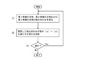
- FIG. 4 is a flow chart showing an example of a processing procedure of a program; A thin film of composition 1 consisting of compound H1, compound DF1 and compound F1, a thin film of composition 2 consisting of compound H1, compound DF2 and compound F1, and a thin film of comparative composition 1 consisting of compound H1, compound DF3 and compound F1.
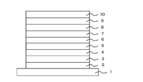
- Emission spectrum. 1 is a schematic diagram showing a laminated structure of an organic electroluminescence element; FIG.
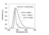
- EL device 2 in which composition 1 was used in the light-emitting layer, EL device 1 in which the concentration of compound F1 was changed to 0.5% by weight, EL device 3 in which the concentration of compound F1 was changed to 2.0% by weight, and compound F1 is an emission spectrum of a comparative EL element 1 that does not contain in the emitting layer.
- the present invention will be described in detail below. Although the constituent elements described below may be described based on representative embodiments and specific examples, the present invention is not limited to such embodiments.
- the numerical range represented by "-" means a range including the numerical values described before and after "-" as lower and upper limits.
- the isotopic species of the hydrogen atoms present in the molecule of the compound used in the present invention is not particularly limited. (deuterium D).
- excitation light used herein refers to light that excites an object to emit light, and light having a wavelength that matches the absorption wavelength of the object can be used.
- the term “host material” refers to a material contained in a mixed film of organic compounds, and an organic compound having the highest lowest excited singlet energy among the organic compounds constituting the mixed film.
- composition contains a first organic compound that satisfies the following conditions (a) to (d), a second organic compound that is a delayed fluorescent material, and a third organic compound that is a fluorescent material.
- E S1 (1) is the lowest excited singlet energy of the first organic compound
- E S1 (2) is the lowest excited singlet energy of the second organic compound
- E S1 (3) is the third organic compound.
- the lowest excited singlet energy, ⁇ E EM (2) is the emission wavelength (unit: nm) on the short wavelength side of the second organic compound, and ⁇ P AB (3) is the peak on the longest wavelength side of the absorption spectrum of the third organic compound.
- the top wavelength (unit: nm) represents the peak top wavelength of the emission spectrum of the second organic compound, and ⁇ P EM (3) represents the peak top wavelength of the emission spectrum of the third organic compound.
- the "delayed fluorescence material" in the present invention is a material that causes reverse intersystem crossing from an excited triplet state to an excited singlet state, and the reverse intersystem crossing occurs due to the absorption of thermal energy, thermally activated A type delayed fluorescence material is preferable.
- a delayed fluorescent material means that when the emission transient decay curve of a thin film (single film) made of the delayed fluorescent material or a mixed film made of the delayed fluorescent material and the host material is observed at 20 ° C., the emission life is short. , and fluorescence with a long emission lifetime (delayed fluorescence) are both observed.
- the “fluorescent material” in the present invention means that when the emission of a thin film (single film) made of the fluorescent material or a mixed film made of the fluorescent material and the host material is observed at 20 ° C., the emission intensity of fluorescence is higher than that of phosphorescence. It is a luminescent material with a higher intensity.
- the "fluorescent material” in the present invention may be a fluorescent material that does not emit delayed fluorescence, or a fluorescent material that emits delayed fluorescence (delayed fluorescent material).
- a fluorescent material that does not emit delayed fluorescence is a fluorescent material from which only fluorescence with a short emission lifetime is observed at 20°C.
- the measurement temperature of the "absorption spectrum” at ⁇ P AB (3) and the "emission spectrum” at ⁇ E EM (2), ⁇ P EM (2) and ⁇ P EM (3) defined in the present invention is 20°C. It is assumed that For specific explanations of the "absorption spectrum” and "emission spectrum”, reference can be made to the explanations in the definitions of physical property values below.
- the lowest excited singlet energy of the first organic compound (E S1 (1)), “the lowest excited singlet energy of the second organic compound” (E S1 (2)), “the lowest Excitation singlet energy” (E S1 (3)) is obtained by measuring the fluorescence spectrum of each thin film of the first organic compound, the second organic compound and the third organic compound (single film of each organic compound) as a measurement sample, It is a value obtained by converting the wavelength ⁇ E EM at the end of the spectrum on the short wave side into an energy value.
- the fluorescence spectrum is a graph showing the emission intensity detected by irradiating the measurement sample with excitation light at 20° C. on the vertical axis and the emission wavelength on the horizontal axis.
- a tangent line is drawn to the rising edge of the fluorescence spectrum on the short wavelength side, and the wavelength ( ⁇ E EM ) [nm] at the intersection of the tangent line and the horizontal axis (end of the fluorescence spectrum on the short wavelength side) is calculated using the following conversion formula.
- the value E S1 converted into an energy value is set to E S1 (1), E S1 (2), or E S1 (3).
- Conversion formula: E S1 [eV] 1239.85/ ⁇ E EM
- the “light emission wavelength on the short wavelength side of the second organic compound (unit: nm)” ( ⁇ E EM (2)) is obtained by using a thin film made of the second organic compound (a single film of the second organic compound) as a measurement sample.
- the emission spectrum is a graph showing the emission intensity detected by irradiating a measurement sample with light while continuously changing the wavelength in the range of 900 to 190 nm on the vertical axis and the wavelength on the horizontal axis.
- a tangent line is drawn to the rising edge of the emission spectrum on the short wavelength side, and the wavelength at the intersection of the tangent line and the horizontal axis (end of the emission spectrum on the short wavelength side) is defined as the wavelength ⁇ E EM (2) [nm].
- the “wavelength of the peak top on the longest wavelength side of the absorption spectrum of the third organic compound (unit nm)” ( ⁇ P AB (3)) in the present invention is a measurement sample of a 10 ⁇ 5 M toluene solution of the third organic compound. It is the maximum absorption wavelength of the absorption peak located on the longest wavelength side in the absorption spectrum measured as . For example, when there are a plurality of absorption peaks in the absorption spectrum, the maximum absorption wavelength of the absorption peak located on the longest wavelength side among them is defined as the wavelength ⁇ P AB (3).
- the “peak top wavelength of the emission spectrum of the second organic compound” ( ⁇ P EM (2)) in the present invention is the emission peak emission of the emission spectrum measured using a mixed film of the second organic compound and the host material as a measurement sample. It is the maximum wavelength.
- the “host material” is an organic compound having a lowest excited singlet energy higher than the lowest excited singlet energy E S1 (2) of the second organic compound, and the concentration of the second organic compound in the mixed film is 30%. % by weight.
- the maximum emission wavelength of the emission peak with the highest intensity is ⁇ P EM (2).
- the “peak top wavelength of the emission spectrum of the third organic compound” ( ⁇ P EM (3)) in the present invention is the emission peak emission of the emission spectrum measured using a mixed film of the third organic compound and the host material as a measurement sample. It is the maximum wavelength.
- the “host material” is an organic compound having a lowest excited singlet energy higher than the lowest excited singlet energy E S1 (3) of the third organic compound, and the concentration of the third organic compound in the mixed film is 1 % by weight.
- the maximum emission wavelength of the emission peak with the highest intensity is ⁇ P EM (3).
- the lower limit of ⁇ P EM (3) is not particularly limited, it is preferably 430 nm or more.
- the composition of the present invention has a TAF (TADF-assisted fluorescent) mechanism and exhibits particularly high-efficiency and high-color-purity light emission, particularly in the wavelength range of less than 480n. provides high color purity.
- TAF TADF-assisted fluorescent
- the mechanism will be described by taking as an example the case where the composition is caused to emit light by current excitation.
- the term “TAF-assisted fluorescent” as used herein means that reverse intersystem crossing occurs in a delayed fluorescent material, thereby converting excited triplet energy into excited singlet energy, and the excited singlet Energy is Förster transferred to the fluorescent material and utilized for fluorescence emission.
- the excited singlet energy generated in the third organic compound transfers Forster to the second organic compound and the third organic compound, and the excited singlet energy generated in the second organic compound , and the excited singlet energy received by the second organic compound from the first organic compound is Förster-transferred to the third organic compound.
- the third organic compound Upon receiving the excited singlet energy, the third organic compound emits fluorescence due to radiation deactivation from the excited singlet state.
- the excited triplet state generated in the second organic compound undergoes reverse intersystem crossing to the excited singlet state, and the excited singlet energy is also applied to the third organic compound. star move. That is, here, the second organic compound functions as an assist dopant that converts excited triplet energy into excited singlet energy and supplies it to the third organic compound. Therefore, in this composition, not only the excited singlet state energy generated by direct excitation, but also the excited triplet energy generated by direct excitation is used for fluorescence emission of the third organic compound, so a delayed fluorescence material is used. A higher luminous efficiency can be obtained as compared with the fluorescent composition without.
- the third organic compound satisfies the condition (d), and the second organic compound and the third organic compound satisfy the conditions (a) and (c), whereby the third organic compound is
- the emitted fluorescence peak has a peak top in a wavelength range of less than 480 nm, and has a narrower peak width than the emission peak when the second organic compound emits light.
- the emission band of the second organic compound and the absorption peak on the longest wavelength side of the third organic compound overlap.
- the composition of the present invention by satisfying the conditions (a) to (d), exhibits particularly high efficiency and high color purity emission, and in particular high color purity in the wavelength range of less than 480 nm. .
- the conditions (a) to (d) are objective indices indicated by numerical magnitude relationships, it is possible to clearly determine whether or not the conditions are satisfied. Therefore, by selecting the first organic compound, the second organic compound, and the third organic compound using the conditions (a) to (d) as indicators, it is possible to reliably realize a composition exhibiting the above characteristics. can be done.
- the second organic compound and the third organic compound preferably satisfy the following condition (b1), and more preferably satisfy the following conditions (b2) to (b4).
- Condition (b1) ⁇ E EM (2) ⁇ ⁇ P AB (3) - 12 nm
- Condition (b2) ⁇ E EM (2) ⁇ ⁇ P AB (3) - 15 nm
- Condition (b3) ⁇ E EM (2) ⁇ ⁇ P AB (3) - 18 nm
- (b4) ⁇ E EM (2) ⁇ ⁇ P AB (3) - 20 nm
- the composition preferably satisfies the following condition (e), and more preferably satisfies the following condition (e1).
- a composition that satisfies the following conditions has a narrow tail width of the emission peak, and therefore exhibits light emission with high color purity.
- Condition (e) FW 0.3M ⁇ 40nm
- Condition (e1) FW 0.3M ⁇ 32nm (In the above formula, FW 0.3M represents the spectral width at a relative intensity of 30% with respect to the emission peak of the emission spectrum of the composition.)
- the second organic compound and the third organic compound preferably satisfy the following conditions (f) and (g).
- electrons and holes are more likely to be injected into the second organic compound than into the third organic compound, and the assist dopant function of the second organic compound can be effectively exhibited.
- Condition (f) LUMO(2) ⁇ LUMO(3)
- Condition (g) HOMO (2) ⁇ HOMO (3) In the above formula, LUMO (2) is the LUMO (Lowest Unoccupied Molecular Orbital) energy of the second organic compound, LUMO (3) is the LUMO energy of the third organic compound, and HOMO (2) is the HOMO of the second organic compound.
- HOMO (3) represents the HOMO energy of the third organic compound.
- the LUMO energy is a value obtained by subtracting the bandgap from the ionization potential measured for a thin film made of the compound to be measured (single film of the compound to be measured), and is a value obtained by adding a “-” sign. is the ionization potential with a minus sign.
- the bandgap is estimated from the wavelength at the end of the absorption spectrum on the longer wavelength side.
- the ionization potential is measured by photoelectron spectroscopy, and for the measurement, for example, a photoelectric spectrometer (manufactured by Riken Keiki Co., Ltd.: AC-3) can be used.
- Condition (h) R 0 (2-3)>6.5 nm (In the above formula, R 0 (2-3) represents the Förster radius between the second organic compound and the third organic compound.)
- the second organic compound and the third organic compound satisfy all of the following conditions (h1), (i1) and (j1).
- R 0 (2-3) r(2-3) and k FRET (2-3) refer to the corresponding definitions of conditions (h), (i) and (j) be able to.
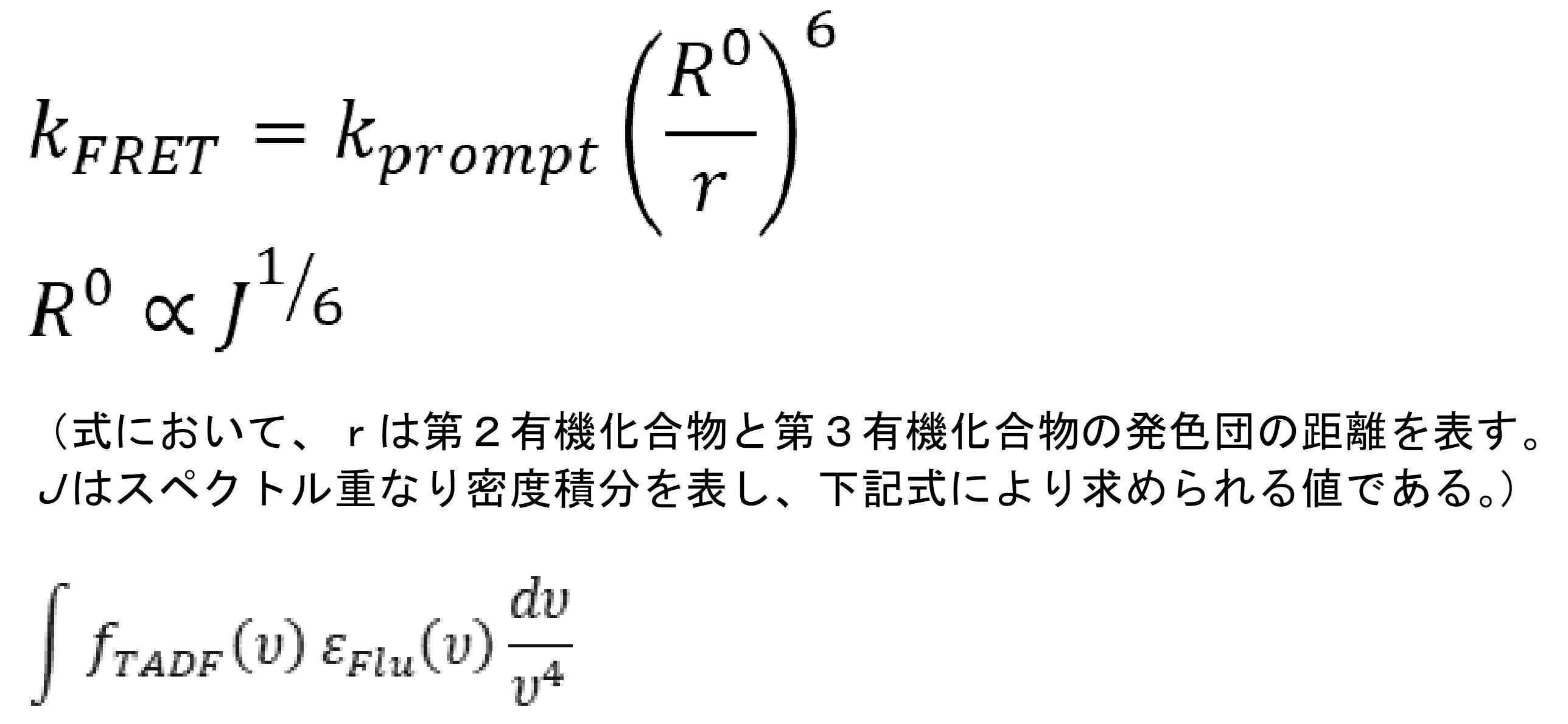
- the “Forster radius between the second organic compound and the third organic compound” (R 0 (2-3)) is a value obtained by the following formula.
- c is the speed of light
- ⁇ PL is the luminous efficiency of the second organic compound
- n is the refractive index of the first organic compound
- NA is the Avogadro constant
- f TADF (v) is the emission spectrum of the second organic compound
- ⁇ Flu (v) represents the absorption spectrum of the third organic compound
- ⁇ represents the wave number.
- the LAMMPS program was used as the MD calculation method, and the most stable structure obtained from the first-principles calculation was used as the initial structure of the molecular structure of each material.
- Gaussian09 a quantum chemical calculation program, was used for the first-principles calculation, and the restabilized structure was calculated by the density approximation method (DFT).
- the distance at which the coordination number is 1 by MD calculation is the value of R 0 (2-3).
- “Förster energy transfer rate k FRET (2-3)” is a value calculated by the following formula.
- the luminescence from the composition of the present invention includes fluorescence from the third organic compound.
- Light emission from the composition of the present invention may contain only the fluorescent component from the third organic compound, or may partially contain the light emitting component from the first organic compound and the second organic compound.
- the largest component of light emission from the composition is preferably fluorescence from the third organic compound.
- the maximum component of light emission from the composition is fluorescence from the third organic compound when the area of the emission peak derived from the third organic compound is more than 50% of the total emission peak area in the emission spectrum of the composition. It can be confirmed by
- the proportion of the fluorescent component derived from the third organic compound in light emitted from the composition is more preferably greater than 60%, more preferably greater than 70%, even more preferably greater than 80%, and 90%. % is particularly preferred.
- Examples of compounds that can be used as the second organic compound include compounds represented by the following general formula (1).
- D represents a substituted or unsubstituted carbazol-9-yl group.
- D may be an unsubstituted carbazol-9-yl group or a carbazol-9-yl group in which at least one of the hydrogen atoms is substituted with a substituent (substituted carbazol-9-yl group).
- the four D's all have the same chemical structure.
- the number of substituents in the substituted carbazol-9-yl group is not particularly limited, and may be 1-8.
- the position of the substituent is not particularly limited, but at least one of the 3- and 6-positions is preferably a substituent.
- a substituted carbazol-9-yl group has two or more substituents
- the multiple substituents may be the same or different.
- substituents in the substituted carbazol-9-yl group include alkyl groups, aryl groups and heteroaryl groups, and these substituents are further substituted with alkyl groups, aryl groups and heteroaryl groups. good too. Adjacent substituents of the carbazol-9-yl group may be bonded to each other to form a cyclic structure.
- Examples of a cyclic structure formed by bonding substituents together include a benzofuran ring, a benzothiophene ring, and an indole ring, and these cyclic structures may be substituted with an alkyl group or an aryl group.
- the alkyl group as a substituent of the carbazol-9-yl group may be linear, branched or cyclic.
- the number of carbon atoms is preferably 1-20, more preferably 1-10, still more preferably 1-6. Examples include methyl group, ethyl group, n-propyl group and isopropyl group.
- the aromatic ring constituting the aryl group may be a single ring, a condensed ring in which two or more aromatic rings are condensed, or a linked ring in which two or more aromatic rings are linked. When two or more aromatic rings are linked, they may be linked in a straight chain or may be linked in a branched form.
- the number of carbon atoms in the aromatic ring constituting the arylene group is preferably 6 to 40, more preferably 6 to 22, even more preferably 6 to 18, and even more preferably 6 to 14. 6 to 10 are particularly preferred.
- Specific examples of aryl groups include phenyl, naphthalenyl, and biphenyl groups.
- a heterocyclic ring constituting a heteroaryl group may be a monocyclic ring or a condensed ring in which one or more heterocyclic rings and one or more aromatic or heterocyclic rings are condensed.
- the heterocyclic ring constituting the heteroaryl group preferably has 3 to 40 carbon atoms, more preferably 5 to 22 carbon atoms, still more preferably 5 to 18 carbon atoms, and even more preferably 5 to 14 carbon atoms. 5 to 12 is particularly preferred.
- a heteroatom constituting the heterocyclic ring is preferably at least one of a nitrogen atom, an oxygen atom and a sulfur atom.
- heteroaryl group examples include carbazol-9-yl group, 10H-phenoxazin-10-yl group, 10H-phenothiazin-10-yl group, 9,10-dihydroacridin-10-yl group, and the like.
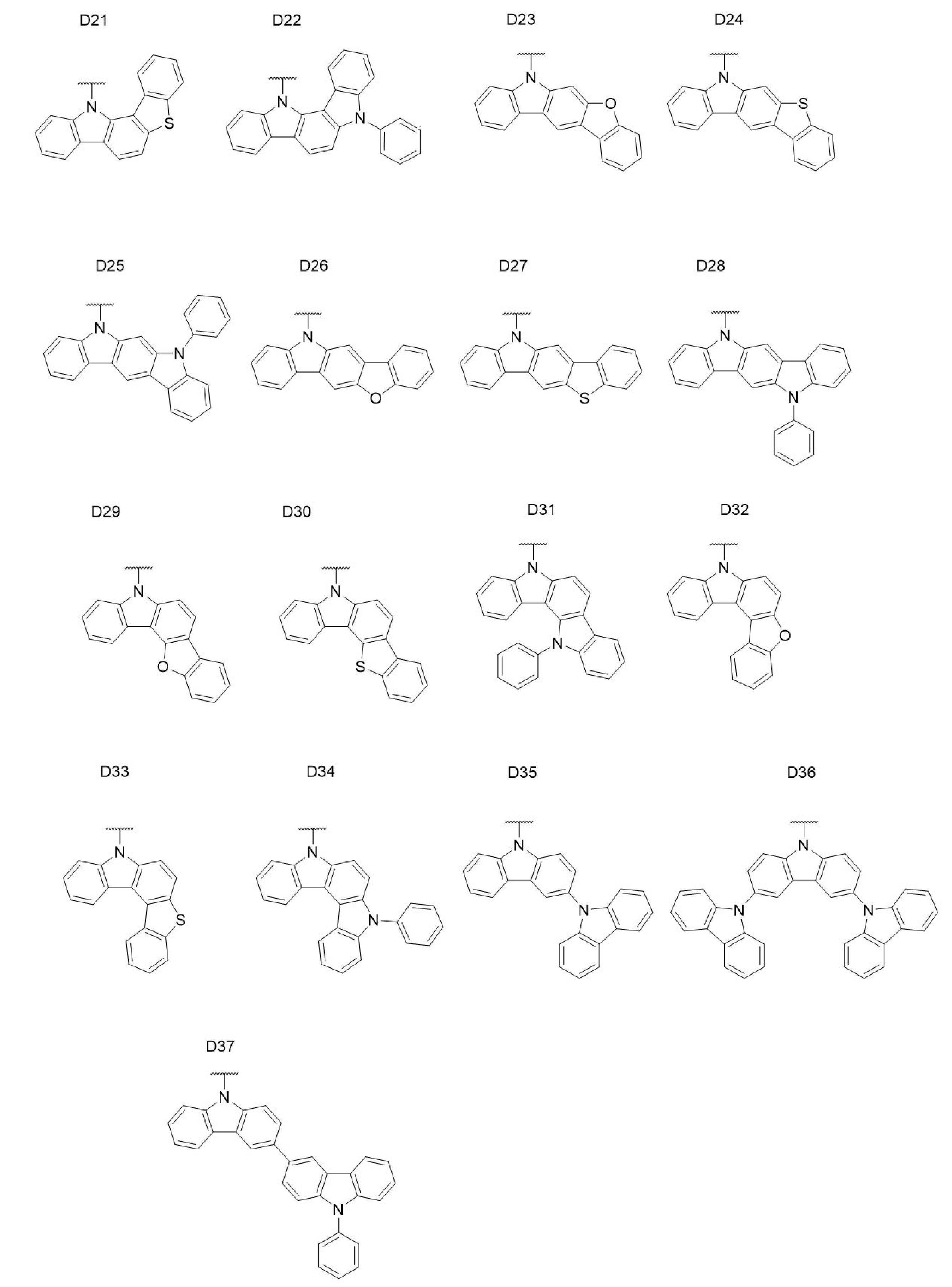
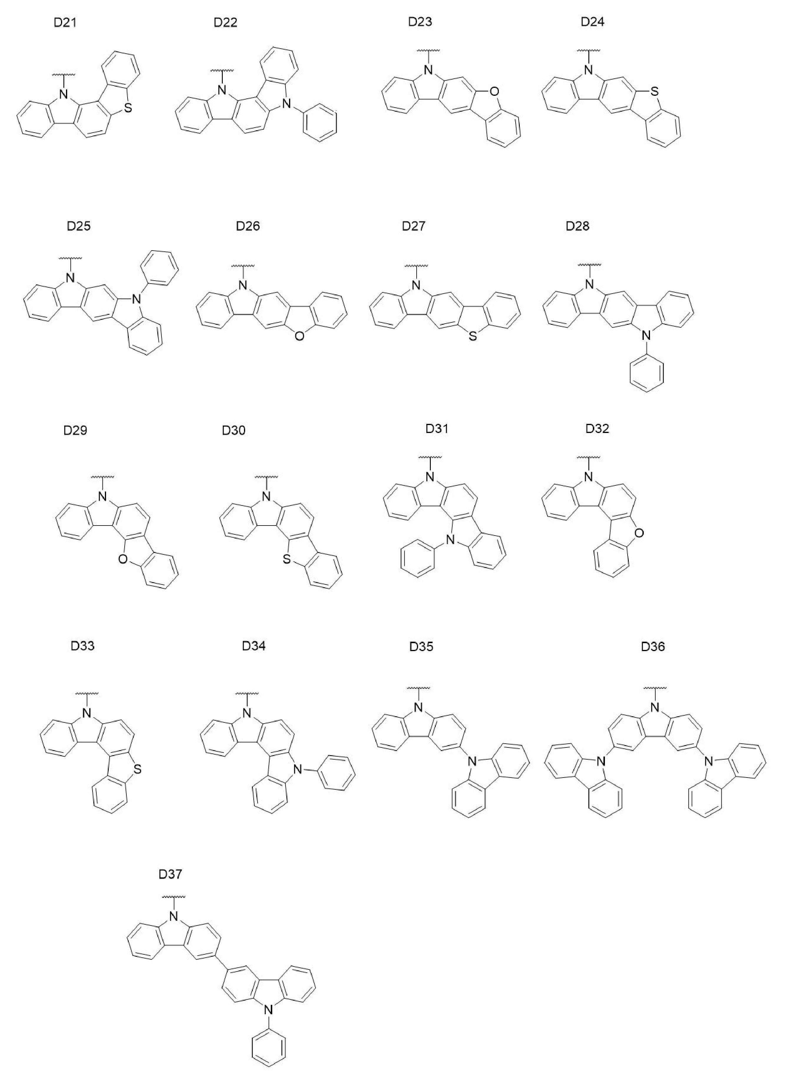
- the substituted carbazol-9-yl group for D preferably has a structure represented by any one of D1 to D37 below.
- the wavy lines in D1 to D37 below represent substitution positions on the benzene ring.
- Ph represents a phenyl group optionally substituted with at least one group selected from the group consisting of an alkyl group, an aryl group and a group to which these are linked.
- at least one group selected from the group consisting of an alkyl group, an aryl group and a group to which these are linked may be referred to as "substituent A”.
- the phenyl group in Ph may be unsubstituted or may be a phenyl group in which at least one hydrogen atom is substituted with a substituent A (substituted phenyl group).
- the number of substituents A is not particularly limited and may be 1-5.
- the position of the substituent A is not particularly limited, and may be any of 2-6 positions.
- the phenyl group has two or more substituents A
- the multiple substituents A may be the same or different.
- preferred range, and specific examples of the alkyl group and aryl group the description, preferred range, and specific examples of the alkyl group and aryl group exemplified as the substituent of the carbazol-9-yl group can be referred to.
- a group in which an alkyl group and an aryl group are linked may be an arylalkyl group or an alkylaryl group.
- the number of aryl groups with which an alkyl group is substituted and the number of alkyl groups with which an aryl group is substituted may be one or two or more.
- the aryl groups may be the same or different.
- the alkyl groups may be the same or different.
- the aryl group as the substituent of the alkyl group and the alkyl group as the substituent of the aryl group may be further substituted with one or more alkyl groups and one or more aryl groups.
- the substitution positions of the four D and Ph on the benzene ring are not particularly limited.
- the substitution position of Ph may be ortho, meta or para to the CN group, preferably para.
- the remaining substitutable positions on the benzene ring are the four D substitution positions regardless of the position of the Ph substitution.
- the compound used as the second organic compound is preferably a compound represented by the following general formula (1a).
- D 1 represents a substituted or unsubstituted carbazol-9-yl group. All four D1's are identical in chemical structure to each other.
- Ph represents a phenyl group optionally substituted with at least one group selected from the group consisting of an alkyl group, an aryl group and a group to which these are linked.
- the description, preferred range, and specific examples of D in the above general formula (1) can be referred to, and the description of Ph With respect to the preferred range and specific examples, the description, preferred range, and specific examples of Ph in the above general formula (1) can be referred to except for the description of the substitution position.
- Examples of compounds that can be used as the second organic compound include compounds represented by the following general formula (2).
- D 1 represents a substituted or unsubstituted carbazol-9-yl group
- D 2 represents a substituted or unsubstituted carbazol-9-yl group different from D 1 .
- the two D2s are identical in chemical structure to each other.
- D 1 and D 2 may be an unsubstituted carbazol-9-yl group or a carbazol-9-yl group in which at least one of the hydrogen atoms is substituted with a substituent (substituted carbazol-9-yl group).
- substituent substituted carbazol-9-yl group
- D 2 in general formula (2) represents a substituted or unsubstituted carbazol-9-yl group different from D 1 .
- the substituted or unsubstituted carbazol-9-yl group represented by D 1 and the substituted or unsubstituted carbazol-9-yl group represented by D 2 have Any of the positions may be different.
- Each of two Ph's independently represents a phenyl group optionally substituted with at least one group selected from the group consisting of an alkyl group, an aryl group and a group to which these are linked. Two Phs may be the same or different.
- a phenyl group optionally substituted with at least one group selected from the group consisting of an alkyl group, an aryl group, and a group to which these are linked represented by Ph
- preferred ranges, and specific examples are described in the above general Description of the "phenyl group optionally substituted with at least one group selected from the group consisting of an alkyl group, an aryl group, and a group to which these are linked” represented by Ph in formula (1), preferred ranges, and specific examples can be referred to.
- the substitution positions of D 1 , D 2 and Ph on the benzene ring are not particularly limited.
- the two Ph substitution positions may be ortho, meta, or para to the CN group, respectively, and in any case, the remaining substitutable positions are D 1 and two D 2 be the replacement position.
- Preferred substitution positions for the two Ph include the ortho and para positions relative to the CN group.
- a preferred substitution position for D2 is the meta position relative to the CN group.
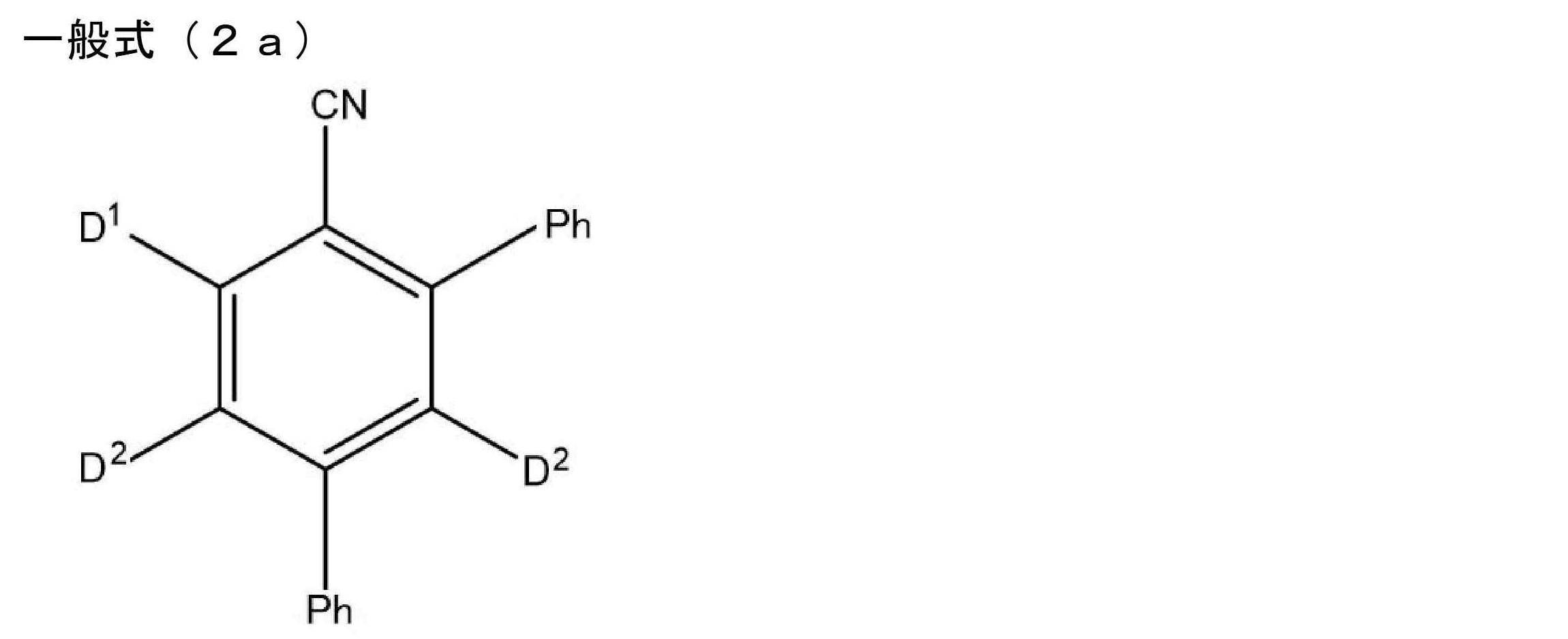
- the compound used as the second organic compound is also preferably a compound represented by the following general formula (2a).
- D 1 represents a substituted or unsubstituted carbazol-9-yl group
- D 2 represents a substituted or unsubstituted carbazol-9-yl group different from D 1 .
- the two D2s have the same chemical structure as each other.
- Each of two Ph's independently represents a phenyl group optionally substituted with at least one group selected from the group consisting of an alkyl group, an aryl group and a group to which these are linked. Two Phs may be the same or different.
- D 1 , D 2 and Ph the description of D 1 , D 2 and Ph in the above general formula (2) can be referred to except for the description of the substitution positions on the benzene ring.
- the third organic compound is preferably a multiple resonance fluorescent material, more preferably a multiple resonance delayed fluorescence material.
- the third organic compound is preferably a compound having multiple resonance between one or more atoms selected from the group consisting of nitrogen atoms, oxygen atoms and sulfur atoms and boron atoms. Cited here as part of the present specification, compounds represented by the general formula and specific compounds described in paragraphs [0011] to [0032] of WO 2020/039930, and represented by the following formula can be preferably used as the third organic compound.
- the first organic compound is an organic compound having a lowest excited singlet energy higher than that of the second organic compound and the second organic compound, and can be selected from known host materials and used, for example. Specific examples of compounds that can be used as the third organic compound are illustrated below. However, the third organic compound that can be used in the present invention should not be construed as being limited by these specific examples.
- the mixing ratio of the first organic compound, the second organic compound and the third organic compound is not particularly limited, but the content of the second organic compound is less than the content of the first organic compound, It is preferable that the content is greater than the content of the third organic compound, that is, the relationship of "content of third organic compound ⁇ content of second organic compound ⁇ content of first organic compound" is satisfied.
- the content of the second organic compound in the composition is preferably less than 50% by weight with respect to the total amount of the first organic compound, the second organic compound and the third organic compound.
- the upper limit of the content of the second organic compound is preferably less than 40% by weight, for example less than 30% by weight, with respect to the total amount of the first organic compound, the second organic compound, and the third organic compound. It may be less than 20% by weight, or less than 10% by weight.
- the lower limit is preferably 0.1% by weight or more, and may be, for example, more than 1% by weight or more than 3% by weight.
- the content of the third organic compound in the composition may be 0.1% by weight or more, or 1% by weight or more with respect to the total amount of the first organic compound, the second organic compound, and the third organic compound. .
- the content of the third organic compound in the composition may be 30% by weight or less, 20% by weight or less, or 10% by weight or less.
- composition of the present invention may consist only of the first organic compound, the second organic compound and the third organic compound, or may contain other components.
- the composition of the present invention exhibits particularly high efficiency and high color purity of light emission, and high color purity is obtained especially in the wavelength range of less than 480 nm. Therefore, the composition of the present invention can be effectively used as a luminescent composition.
- the mode of use is not particularly limited. and a mode in which the composition is dissolved in a solvent and used as a liquid light-emitting material.
- the descriptions in the following sections ⁇ Film> and ⁇ Light-emitting film> can be referred to.
- the membrane of the invention is characterized by comprising the composition of the invention.
- the description in the ⁇ Composition> section above can be referred to.
- the composition of the present invention exhibits luminescence with particularly high efficiency and high color purity, and particularly high color purity in the wavelength range of less than 480 nm. Shows excellent characteristics reflecting the characteristics of
- the film of the present invention can be formed as follows.
- films comprising compositions of the invention can be formed in a wet process.
- a solution of the composition of the invention is applied to the surface and a film is formed after removal of the solvent.
- wet processes include spin coating, slit coating, inkjet (spray), gravure printing, offset printing, and flexographic printing, but are not limited to these.
- a suitable organic solvent is selected and used that is capable of dissolving the composition of the present invention.
- organic compounds included in the composition can be introduced with substituents (eg, alkyl groups) that increase solubility in organic solvents.
- films comprising compositions of the invention can be formed in a dry process.
- the dry process can be vacuum deposition, but is not limited to this.
- each organic compound constituting the composition may be co-deposited from individual deposition sources, or may be co-deposited from a single deposition source in which each organic compound is mixed.
- a single vapor deposition source is used, a mixed powder obtained by mixing powders of the respective organic compounds may be used, a compression molding obtained by compressing the mixed powder may be used, or each organic compound may be heated and melted. A cooled mixture may be used.
- the vapor deposition rate (weight reduction rate) of the plurality of organic compounds contained in a single vapor deposition source is the same or substantially the same, so that the vapor deposition rate of the plurality of organic compounds contained in the vapor deposition source is reduced.
- a film having a composition ratio corresponding to the composition ratio can be formed.
- a film having a desired composition ratio can be easily formed by mixing a plurality of organic compounds at the same composition ratio as that of the film to be formed and using the mixture as an evaporation source.
- the temperature at which each co-evaporated organic compound has the same weight loss rate can be identified and used as the temperature during co-evaporation.
- the membranes of the present invention may be of single-layer or multi-layer construction.
- the layers may differ in at least one of the first organic compound, the second organic compound and the third organic compound, or may differ in composition ratio. or the presence or absence of other components may differ from each other.
- the thickness of the film of the present invention is preferably 10-100 nm, more preferably 20-60 nm, even more preferably 30-50 nm.
- the preferred thickness range of each film is the above thickness range.
- the films of the present invention exhibit particularly efficient and highly chromatically pure light emission, particularly in the wavelength range below 480 nm. Therefore, the film of the present invention can be effectively used as a light-emitting film.
- the description in the above ⁇ film> section can be referred to.
- the light-emitting film of the present invention can be effectively used as a light-emitting layer of an organic light-emitting device.
- the description in the section ⁇ Organic Light-Emitting Device> below can be referred to.
- the composition of the present invention contains the first organic compound, the second organic compound, and the third organic compound that satisfy predetermined conditions, the TAF mechanism works to exhibit light emission with particularly high efficiency and high color purity, particularly at 480 nm. High color purity is obtained in the wavelength range of Therefore, the composition of the present invention can be effectively used as a material for a light-emitting layer of a TAF type organic light-emitting device, and is particularly suitable as a material for a light-emitting layer of an organic electroluminescence device.
- the ratio of the fluorescent component derived from the third organic compound in the light emitted from the device is more preferably over 60%, more preferably over 70%, even more preferably over 80%, and even more preferably over 90%. More than is particularly preferred.
- the wavelength of the emission peak derived from the third organic compound is not limited, but in a preferred embodiment it is in the blue emission region (400 nm to 490 nm), and in a more preferred embodiment it is 420 nm to 480 nm.
- the organic layer includes at least a light-emitting layer, may consist of only the light-emitting layer, or may have one or more organic layers in addition to the light-emitting layer. There may be.
- Such other organic layers can include hole transport layers, hole injection layers, electron blocking layers, hole blocking layers, electron injection layers, electron transport layers, exciton blocking layers, and the like.
- the hole transport layer may be a hole injection transport layer having a hole injection function
- the electron transport layer may be an electron injection transport layer having an electron injection function.
- the organic electroluminescence device of the present invention may be of the bottom emission type in which light is emitted from the substrate side, or may be of the top emission type in which light is emitted from the side opposite to the substrate, but is of the top emission type. is preferred.
- the electrode (one electrode) on the substrate side of the pair of electrodes is composed of a transparent electrode
- the substrate and the The electrode on the opposite side (one electrode) is composed of a transparent electrode.
- the other electrode may be a transparent electrode, a semi-transparent electrode, or a reflective electrode.
- a reflective layer formed of a single metal or an alloy is adjacent to the electrode. may be provided.
- materials that can be used for organic electroluminescence elements are specifically exemplified below.
- materials that can be used in the present invention are not limited to the following exemplary compounds.
- compounds exemplified as materials having specific functions can be used as materials having other functions.
- the following compounds can be preferably used as electron blocking materials.
- the following compounds are preferably used as hole blocking materials.
- the first organic compound, the second organic compound as the delayed fluorescent material, and the third organic compound as the fluorescent material are selected so as to satisfy the above conditions (a) to (d).
- a method of designing a composition comprising a first organic compound, a second organic compound and a third organic compound, characterized by:
- the first organic compound, the second organic compound, and the third organic compound are preferably selected so as to satisfy the above conditions (f) and (g). It is also preferable to satisfy at least one of (h), (i) and (j), and more preferably to satisfy all of the above conditions (h1), (i1) and (j1).
- the selection of the first organic compound, the second organic compound, and the third organic compound may be performed so as to satisfy the above conditions (a) to (d). It is preferable that conditions (f) and (g) are also satisfied, or at least one of conditions (h), (i) and (j) is also satisfied, conditions (f) and (g) are also satisfied, and conditions More preferably, at least one of (h), (i) and (j) is also satisfied, conditions (f) and (g) are also satisfied, and conditions (h1), (i1) and (j1) It is particularly preferable to do so that all are satisfied.
- conditions (a) to (d), (f) to (j), and (h1) to (j1) For the description of the conditions (a) to (d), (f) to (j), and (h1) to (j1), the description in the ⁇ Composition> section above can be referred to.
- a composition of organic compounds satisfying conditions (a) to (d), preferably conditions (a) to (d) and conditions (f) to (j), (h1) to (j1) ) exhibits particularly high efficiency and high color purity, and high color purity can be obtained particularly in the wavelength range of less than 480 nm.
- conditions (a) to (d), (f) to (j) and (h1) to (j1) are objective indexes indicated by numerical magnitude relationships, and thus satisfy the conditions.
- the first organic compound, the second organic compound, and the third organic compound are selected so as to satisfy conditions (a) to (d), conditions (f) to (j), and (h1) to (j1).
- the population from which the first organic compound, the second organic compound and the third organic compound are to be selected includes the above [first organic compound], [second organic compound] and [third organic compound].
- Compound groups exemplified in the column can be used.
- the selection targets used in the designing method of the present invention should not be construed as limited by these compound examples.
- the program of the present invention is a program for carrying out the method of designing the composition of the present invention.
- the description in the section ⁇ Method for designing composition> can be referred to.
- the program of the present invention includes, for example, a database storing compound group E S1 (1) that can be used as the first organic compound, compound group E S1 (2) that can be used as the second organic compound, ⁇ E EM (2), and With reference to a database storing ⁇ P EM (2) and a database storing compound groups E S1 (3), ⁇ P AB (3) and ⁇ P EM (3) that can be used as the third organic compound, the conditions A step of selecting a combination of the first organic compound, the second organic compound, and the third organic compound that satisfies (a) to (d).
- the program of the present invention performs R 0 (2-3), r(2-3) and k FRET (2-3) for the combination of the second organic compound and the third organic compound selected in the above steps.
- step S1 and step S2 are repeated for one cycle or more (S3).
- the judgment result can be displayed on a display or printed out.
- the determination result may be output for each cycle of steps S1 and S2, or may be collectively output after all cycles are completed.
- the subprogram may determine whether the cycle should be repeated. For example, it is possible to use a subprogram that issues a command to repeat the cycle until a specified number or more of combinations satisfying all of the conditions (a) to (d) are found. If the cycle is to be repeated one or more times, step S1 assumes a new combination different from the previously assumed combination. At this time, any one of the first organic compound, the second organic compound and the third organic compound may be changed, any two may be changed, or all three may be changed. may Alternatively, a subprogram may be used in step S1 in which candidate first organic compounds, second organic compounds, and third organic compounds are read in advance, and combinations of these candidate compounds are sequentially output. In addition, modifications that are obvious to those skilled in the art can be made as appropriate.
- the emission characteristics were evaluated using an absorption spectrometer (SHIMAZU: UV-2550) and an absolute PL quantum yield spectrometer (Hamamatsu Photonics), and optical calculations were performed using optical calculation software (FLUXiM : setfos) using the refractive index of the material, the luminous efficiency of the luminescent material actually measured with an integrating sphere, and the PL spectrum data actually measured.
- the compounds used in the following Examples and Comparative Examples are shown below.
- the compound H1 shown in the column of host material corresponds to the first organic compound
- the compound DF1 or DF2 shown in the column of delayed fluorescent material corresponds to the second organic compound
- the compound shown in the column of fluorescent material corresponds to the second organic compound.
- Compound F1 corresponds to the third organic compound.
- Tables 1 to 3 show the physical properties of the compounds used in each example and each comparative example.
- Table 4 shows the compositions of the compositions used in each example and each comparative example.
- composition 1 and composition 2 are compositions that satisfy all conditions (f) to (j) in addition to conditions (a) to (d) defined in the present invention.
- Example 1 Preparation and evaluation of thin film (Example 1) Preparation of thin film of composition 1 Using a vacuum deposition method, under conditions of a degree of vacuum of 1 ⁇ 10 -6 Pa, a compound H1, a compound DF1, and a compound are formed on a quartz substrate. F1 was deposited from a different deposition source to form a 40 nm thick thin film (Composition 1). At this time, the composition ratio of each compound (compound H1:compound DF1:compound F1) was 69:30:1.0 (weight ratio).
- composition 2 Preparation of thin film of composition 2
- composition 2 was formed in the same manner as in Example 1, except that compound DF2 was used instead of compound DF1.
- Comparative Example 1 Preparation of Thin Film of Comparative Composition 1 A thin film (comparative composition 1) was formed in the same manner as in Example 1, except that compound DF3 was used instead of compound DF1.
- Comparative Example 2 Preparation of Thin Film of Comparative Composition 2
- compound H2 was used instead of compound H1
- compound DF4 was used instead of compound DF1
- compound F2 was used instead of compound F1.
- a thin film was formed in the same manner.
- Table 5 shows the measurement results of the chromaticity coordinates.
- the luminescence observed in the thin films of composition 1 and composition 2 had a FW of 0.3M of less than 40 nm and a small y value of the chromaticity coordinate, indicating high color purity.
- the emission from Comparative Composition 1, which did not satisfy the condition (b) had a broad peak shape, a wide FW of 0.3M of 54.5 nm, and low color purity.
- the thin film of Comparative Composition 2 that did not satisfy the condition (b) was also measured for the emission spectrum with excitation light of 365 nm, it was found to have a broad peak shape with a widened tail. From this, it can be seen that the color purity is greatly improved by forming a composition using three types of organic compounds that satisfy the conditions (a) to (d), compared to a composition that does not satisfy the condition (b). I found out.
- Example 3 Production of an organic electroluminescence device using composition 1 for a light-emitting layer Each thin film was vacuum-coated on a glass substrate 1 on which an anode 2 made of indium tin oxide (ITO) with a thickness of 50 nm was formed. Lamination was performed at a degree of vacuum of 1 ⁇ 10 ⁇ 6 Pa by a vapor deposition method. First, HATCN was deposited on ITO to a thickness of 10 nm to form the hole injection layer 3 .
- ITO indium tin oxide
- ⁇ -NPD was deposited to a thickness of 35 nm to form a first hole transport layer 4, and TrisPCz was deposited thereon to a thickness of 10 nm to form a second hole transport layer 5.
- an electron blocking layer 6 was formed by vapor-depositing mCBP to a thickness of 5 nm.
- a light-emitting layer made of Composition 1 was formed. Specifically, the compound H1, the compound DF1, and the compound F1 were co-evaporated from different evaporation sources to form a layer having a thickness of 40 nm to form the light-emitting layer 7 .
- the composition ratio of each compound was 69:30:1.0 (weight ratio).
- the compound a was deposited to a thickness of 10 nm to form a hole blocking layer 8, and the compound a and Liq were co-deposited thereon from different deposition sources to form a hole transport layer having a thickness of 30 nm. 9 was formed.
- the composition ratio (compound a:Liq) of each compound was 70:30 (weight ratio).
- Liq was vapor-deposited to a thickness of 2 nm to form an electron injection layer 10
- Al was vapor-deposited to a thickness of 100 nm to form a cathode 11 thereon.
- Example 4 Preparation of organic electroluminescence devices with different composition ratios of light-emitting layers
- the composition ratio of the light-emitting layers (compound H1: compound DF1: compound F1) was 69.5:30:0.5 (weight ratio).
- An organic electroluminescence device (EL device 2) was produced in the same manner as in Example 3, except that Separately from this, organic electroluminescence was performed in the same manner as in Example 3, except that the composition ratio of the light-emitting layer (compound H1: compound DF1: compound F1) was 68:30:2.0 (weight ratio).
- An element (EL element 3) was produced.
- Comparative Example 4 Production of an organic electroluminescence device using Comparative Composition 1 for the light-emitting layer The procedure of Example 3 was repeated except that the composition of Comparative Composition 1 was used instead of Composition 1 to form a light-emitting layer. An organic electroluminescence device (comparative EL device 2) was produced.
- FIG. 4 shows emission spectra measured for each of the EL devices produced in Examples 3 to 5 and Comparative Example 3.
- FIG. 4 the numbers in parentheses indicate the concentration of compound F1 in the light-emitting layer.
- the driving voltage, external quantum efficiency (EQE), CIE chromaticity coordinates and emission peak top wavelength (emission maximum wavelength) are shown in Table 6.
- the emission peaks of EL devices 1 to 3 clearly have narrower peak widths than the emission peak of comparative EL device 1 .
- EL devices 1 to 3 have higher external quantum efficiencies than comparative EL device 1, and have smaller y values in the chromaticity coordinates than comparative EL devices 1 and 2. indicated purity. From this, it can be seen that by configuring the light-emitting layer using three kinds of organic compounds that satisfy the conditions (a) to (d), the efficiency and color purity are improved compared to the device that does not use the third organic compound. It was found that the color purity is improved as compared with the element that uses the organic compound of the above type but does not satisfy the condition (b).
- the top emission type EL elements are top emission type organic electroluminescence elements in which the following layer structure is laminated on a glass substrate. In the layer structure below, “/" indicates the boundary between layers, and the numbers in parentheses are the thickness of each layer.
- the “APC reflective layer” is an alloy layer having a composition of Ag: 98% by weight, Pd: 1% by weight, Cu: 1% by weight, and the APC reflective layer side is arranged on the glass substrate side. .
- the “composition” is the composition constituting the light-emitting layer, which is composition 1 for EL device 5, composition 2 for EL device 6, and comparative composition 1 for comparative EL device 3.
- EL device 1 using composition 1 and EL device 4 using composition 2 have higher color purity than comparative EL device 2 using comparative composition 1 (the y value of the chromaticity coordinates is EL element 5 using composition 1 and EL element 6 using composition 2 have higher color purity than comparative EL element 3 using comparative composition 1 (the y value of the chromaticity coordinate is smaller).
- the top emission type EL elements 5 and 6 are greatly improved in emission intensity compared to the top emission type comparative EL element 3 . From this, when the light-emitting layer is formed using three types of organic compounds that satisfy the conditions (a) to (d), the color purity is improved compared to those that do not satisfy the condition (b), especially in the top emission type. , the emission intensity was greatly improved.
- the materials of the organic electroluminescence device used in layers other than the light-emitting layer are shown below.
- the composition of the present invention is a composition that emits light by the TAF mechanism, and exhibits light emission with high efficiency and high color purity. Therefore, by using the composition of the present invention, a TAF-type organic light-emitting device with high efficiency and high color purity can be easily realized. Therefore, the present invention has high industrial applicability.
Landscapes
- Chemical & Material Sciences (AREA)
- Engineering & Computer Science (AREA)
- Materials Engineering (AREA)
- Physics & Mathematics (AREA)
- Spectroscopy & Molecular Physics (AREA)
- Organic Chemistry (AREA)
- Optics & Photonics (AREA)
- Electroluminescent Light Sources (AREA)
Abstract
Description
すなわち、有機発光素子の発光層で電子と正孔が再結合すると、スピン統計則に従って励起一重項状態と励起三重項状態が25%:75%の確率で生成する。ここで、通常の蛍光材料では、励起三重項状態は熱を放出して無輻射失活するため、25%相当分の励起一重項エネルギーしか発光に利用されず、発光効率に理論上の限界がある。一方、遅延蛍光材料は、励起三重項状態から励起一重項状態への逆項間交差を起こす有機化合物である。そのため、遅延蛍光材料と蛍光材料を組み合わせて発光層に用いると、遅延蛍光材料にて励起三重項エネルギーが励起一重項エネルギーに変換されて蛍光材料にフェルスター移動し、そのエネルギーを受け取った蛍光材料も励起一重項状態から輻射失活して発光する。こうしたメカニズムにより、TAF型有機発光素子では、直接励起により生成した励起一重項エネルギーとともに、直接励起により生成した励起三重項エネルギーも蛍光発光に利用されるため、高い発光効率を示す。
そして、近年では、さらに遅延蛍光材料と発光材料の組み合わせを工夫することにより、より優れたTAF型有機発光素子が提案されている。
非特許文献1には、青色、緑色、黄色および赤色の汎用の蛍光材料と、特定の遅延蛍光材料を組み合わせて用いたTAF型有機発光素子において、遅延蛍光材料から蛍光材料へのエネルギー移動が効率よく起こり、高い発光効率を示したことが記載されている。
非特許文献2には、特定の黄色蛍光材料と、4つの3,6-ジメチルカルバゾール-9-イル基で置換されたジシアノベンゼンを遅延蛍光材料として組み合わせたTAF型有機発光素子において、励起一重項エネルギーのフェルスター移動が効率よく起こり、動作安定性が向上したことが記載されている。
条件(a) ES1(1)> ES1(2)> ES1(3)
条件(b) λE EM(2)< λP AB(3)-10nm
条件(c) λP EM(3)< λP EM(2)
条件(d) λP EM(3)< 480nm
(上式において、ES1(1)は前記第1有機化合物の最低励起一重項エネルギー、ES1(2)は前記第2有機化合物の最低励起一重項エネルギー、ES1(3)は前記第3有機化合物の最低励起一重項エネルギー、λE EM(2)は前記第2有機化合物の短波長側の発光波長(単位nm)、λP AB(3)は前記第3有機化合物の吸収スペクトルの最も長波長側のピークトップの波長(単位nm)、λP EM(2)は前記第2有機化合物の発光スペクトルのピークトップの波長、λP EM(3)は前記第3有機化合物の発光スペクトルのピークトップの波長を表す。)
[2] 下記条件(e)を満たす、[1]に記載の組成物。
条件(e) FW0.3M < 40nm
(上式において、FW0.3M は前記組成物の発光スペクトルの発光ピークに対する相対強度が30%におけるスペクトル幅を表す。)
[3] 下記条件(e1)を満たす、[2]に記載の組成物。
条件(e1) FW0.3M < 32nm
[4] 下記条件(f)および(g)を満たす、[1]~[3]のいずれか1項に記載の組成物。
条件(f) LUMO(2)≦ LUMO(3)
条件(g) HOMO(2)≦ HOMO(3)
(上式において、LUMO(2)は前記第2有機化合物のLUMOのエネルギー、LUMO(3)は前記第3有機化合物のLUMOのエネルギー、HOMO(2)は前記第2有機化合物のHOMOのエネルギー、HOMO(3)は前記第3有機化合物のHOMOのエネルギーを表す。)
[5] 下記条件(h)を満たす、[1]~[4]のいずれか1項に記載の組成物。
条件(h) R0(2-3)> 6.5nm
(上式において、R0(2-3)は、前記第2有機化合物と前記第3有機化合物との間のフェルスター半径を表す。)
[6] 下記条件(i)を満たす、[1]~[5]のいずれか1項に記載の組成物。
条件(i) r(2-3)< 3.91nm
(上式において、r(2-3)は、前記第2有機化合物と前記第3有機化合物との間の分子間距離を表す。)
[7] 下記条件(j)を満たす、[1]~[6]のいずれか1項に記載の組成物。
条件(j) kFRET(2-3)> 1.5×10⁹s-1
(上式において、kFRET(2-3)は、前記第2有機化合物と前記第3有機化合物との間のフェルスターエネルギー移動速度定数を表す。)
[8] 下記条件(h1)、(i1)および(j1)を満たす、[1]~[4]のいずれか1項に記載の組成物。
条件(h1) R0(2-3)≧ 7.3nm
条件(i1) r(2-3)≦ 3.71nm
条件(j1) kFRET(2-3)≧ 6.1×10⁹s-1
(上式において、
R0(2-3)は、前記第2有機化合物と前記第3有機化合物との間のフェルスター半径、r(2-3)は、前記第2有機化合物と前記第3有機化合物との間の分子間距離、kFRET(2-3)は、前記第2有機化合物と前記第3有機化合物との間のフェルスターエネルギー移動速度定数を表す。)
[9] 前記有機第2化合物が下記一般式(1)で表される構造を有する、[1]~[8]のいずれか1項に記載の組成物。
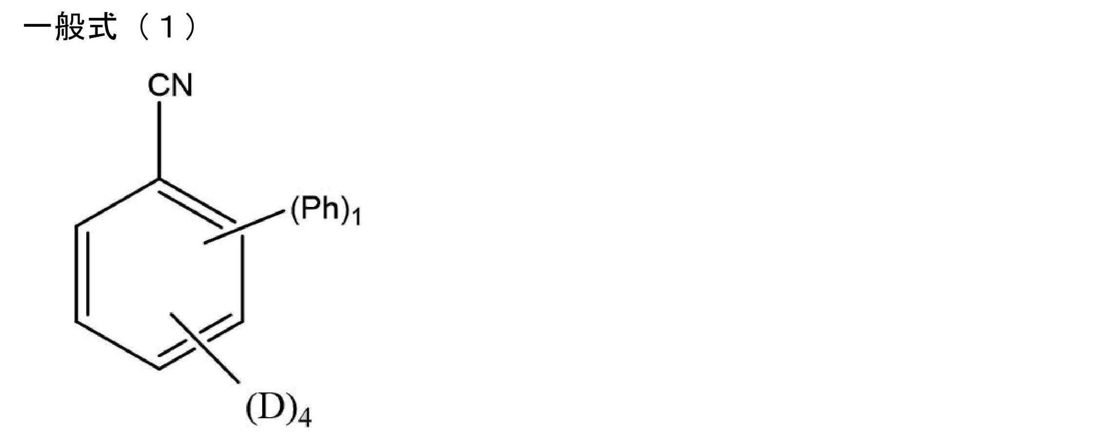
[10] 前記有機第2化合物が下記一般式(1a)で表される構造を有する、[9]に記載の組成物。

[11] 前記有機第2化合物が下記一般式(2)で表される構造を有する、[1]~[8]のいずれか1項に記載の組成物。

[12] 前記有機第2化合物が下記一般式(2a)で表される構造を有する、[11]に記載の組成物。
[13] D、D1およびD2が、各々独立に下記D1~D37のいずれかで表される構造を有する、[9]~[12]のいずれか1項に記載の組成物。

[15] [1]~[13]のいずれか1項に記載の組成物の発光組成物を含む膜。
[16] [15]に記載の膜の発光膜としての使用。
[17] 陽極、陰極、および前記陽極と前記陰極の間に発光層を含む少なくとも一層の有機層を有する有機エレクトロルミネッセンス素子であって、前記発光層は、[1]~[13]のいずれか1項に記載の組成物を含み、前記素子からの発光の最大成分は前記第3有機化合物からの蛍光である、有機エレクトロルミネッセンス素子。
[18] トップエミッション型である、[17]に記載の有機エレクトロルミネッセンス素子。
[19] 上記条件(a)~(d)を満たすように第1有機化合物と遅延蛍光材料である第2有機化合物と蛍光材料である第3有機化合物を選択することを特徴とする、第1有機化合物と第2有機化合物と第3有機化合物を含む組成物の設計方法。
[20] 前記選択を、上記条件(f)および(g)も満たすように行う、[19]に記載の組成物の設計方法。
[21] 前記選択を、上記条件(h)も満たすように行う、[19]または[20]に記載の組成物の設計方法。
条件(h) R0(2-3)> 6.5nm
(上式において、R0(2-3)は、前記第2有機化合物と前記第3有機化合物との間のフェルスター半径を表す。)
[22] 前記選択を、上記条件(i)も満たすように行う、[19]~[21]のいずれか1項に記載の組成物の設計方法。
[23] 前記選択を、上記条件(j)も満たすように行う、[19]~[22]のいずれか1項に記載の組成物の設計方法。
[24] 前記選択を、上記条件(h1)、(i1)および(j1)も満たすように行う、[19]に記載の組成物の設計方法。
[25] [19]~[24]のいずれか1項に記載の組成物の設計方法を実施するためのプログラム。
本明細書における「励起光」とは、対象物に励起を引き起こして発光を生じさせる光であり、その対象物の吸収波長に一致する波長の光を用いることができる。
本明細書における「ホスト材料」とは、有機化合物の混合膜に含まれる材料であって、混合膜を構成する有機化合物の中で、最低励起一重項エネルギーが最も高い有機化合物のことをいう。
本発明の組成物は、下記条件(a)~(d)を満たす第1有機化合物と遅延蛍光材料である第2有機化合物と蛍光材料である第3有機化合物を含むものである。
条件(a) ES1(1)> ES1(2)> ES1(3)
条件(b) λE EM(2)< λP AB(3)-10nm
条件(c) λP EM(3)< λP EM(2)
条件(d) λP EM(3)< 480nm
(上式において、ES1(1)は第1有機化合物の最低励起一重項エネルギー、ES1(2)は第2有機化合物の最低励起一重項エネルギー、ES1(3)は第3有機化合物の最低励起一重項エネルギー、λE EM(2)は第2有機化合物の短波長側の発光波長(単位nm)、λP AB(3)は第3有機化合物の吸収スペクトルの最も長波長側のピークトップの波長(単位nm)、λP EM(2)は第2有機化合物の発光スペクトルのピークトップの波長、λP EM(3)は第3有機化合物の発光スペクトルのピークトップの波長を表す。)
本発明における「遅延蛍光材料」とは、励起三重項状態から励起一重項状態への逆項間交差を起こす材料であり、逆項間交差が熱エネルギーの吸収に起因して起こる、熱活性化型遅延蛍光材料であることが好ましい。遅延蛍光材料であることは、その遅延蛍光材料からなる薄膜(単独膜)またはその遅延蛍光材料とホスト材料からなる混合膜の発光過渡減衰曲線を20℃で観測したとき、発光寿命が短い蛍光と、発光寿命が長い蛍光(遅延蛍光)の両方が観測されることをもって判定することとする。
本発明における「蛍光材料」とは、その蛍光材料からなる薄膜(単独膜)またはその蛍光材料とホスト材料からなる混合膜の発光を20℃で観測したとき、燐光の発光強度よりも蛍光の発光強度の方が高い発光材料である。通常の蛍光(遅延蛍光ではない蛍光)は、発光寿命がnsオーダーであり、燐光は、通常、発光寿命がmsオーダーであるため、蛍光と燐光とは発光寿命により区別することができる。本発明における「蛍光材料」は、遅延蛍光を放射しない蛍光材料であってもよいし、遅延蛍光を放射する蛍光材料(遅延蛍光材料)であってもよい。ここで、「遅延蛍光を放射しない蛍光材料」とは、20℃で発光寿命が短い蛍光のみが観測される蛍光材料である。
本発明で規定するλP AB(3)における「吸収スペクトル」、λE EM(2)、λP EM(2)およびλP EM(3)における「発光スペクトル」の測定温度は20℃であることとする。「吸収スペクトル」および「発光スペクトル」の具体的な説明については、下記の物性値の定義における説明を参照することができる。
換算式:ES1[eV]=1239.85/λE EM
本発明における「第2有機化合物の短波長側の発光波長(単位nm)」(λE EM(2))は、第2有機化合物からなる薄膜(第2有機化合物の単独膜)を測定試料として測定した発光スペクトルの短波長側のスペクトル端の波長である。発光スペクトルは、900~190nmの範囲で波長を連続的に変化させながら、測定試料に光照射して検出される発光強度を縦軸、波長を横軸に示したグラフである。その発光スペクトルの短波長側の立ち上がりに対して接線を引き、その接線と横軸との交点(短波長側の発光スペクトル端)における波長を波長λE EM(2)[nm]とする。
本発明における「第3有機化合物の吸収スペクトルの最も長波長側のピークトップの波長(単位nm)」(λP AB(3))は、第3有機化合物の10-5Mトルエン溶液を測定試料として測定した吸収スペクトルの中で、最も長波長側に位置する吸収ピークの吸収極大波長である。例えば、吸収スペクトルに吸収ピークが複数存在する場合には、その中で、最も長波長側に位置する吸収ピークの吸収極大波長を波長λP AB(3)とする。
本発明における「第2有機化合物の発光スペクトルのピークトップの波長」(λP EM(2))は、第2有機化合物とホスト材料の混合膜を測定試料として測定した発光スペクトルの発光ピークの発光極大波長である。ここで、「ホスト材料」は、第2有機化合物の最低励起一重項エネルギーES1(2)よりも高い最低励起一重項エネルギーを有する有機化合物であり、混合膜における第2有機化合物の濃度は30重量%とする。発光スペクトルに複数の発光ピークが存在するときは、最も強度が大きな発光ピークの発光極大波長がλP EM(2)であることとする。
本発明における「第3有機化合物の発光スペクトルのピークトップの波長」(λP EM(3))は、第3有機化合物とホスト材料の混合膜を測定試料として測定した発光スペクトルの発光ピークの発光極大波長である。ここで、「ホスト材料」は、第3有機化合物の最低励起一重項エネルギーES1(3)よりも高い最低励起一重項エネルギーを有する有機化合物であり、混合膜における第3有機化合物の濃度は1重量%とする。発光スペクトルに複数の発光ピークが存在するときは、最も強度が大きな発光ピークの発光極大波長がλP EM(3)であることとする。λP EM(3)の下限は特に制限されないが、430nm以上であることが好ましい。
まず、本発明の組成物に電子と正孔が注入されると、その電子と正孔の再結合により、各有機化合物において励起一重項状態と励起三重項状態が25:75の生成確率で生成する。ここで、条件(a)を満たすことにより、第3有機化合物で生成した励起一重項エネルギーは第2有機化合物と第3有機化合物にフェルスター移動し、第2有機化合物で生成した励起一重項エネルギー、および、第2有機化合物が第1有機化合物から受け取った励起一重項エネルギーは、第3有機化合物にフェルスター移動する。そして、励起一重項エネルギーを受け取った第3有機化合物は、励起一重項状態からの輻射失活により蛍光を放射する。また、第2有機化合物は遅延蛍光材料であるため、第2有機化合物で生成した励起三重項状態は励起一重項状態へと逆項間交差し、その励起一重項エネルギーも第3有機化合物にフェルスター移動する。すなわち、ここでは、第2有機化合物が励起三重項エネルギーを励起一重項エネルギーに変換して第3有機化合物へ供給するアシストドーパントとして機能する。したがって、この組成物では、直接励起により生成した励起一重項状態のエネルギーのみならず、直接励起により生成した励起三重項エネルギーも第3有機化合物の蛍光発光に利用されるため、遅延蛍光材料を用いない蛍光組成物に比べて高い発光効率が得られる。
ここで、本発明の組成物では、第3有機化合物が条件(d)を満たし、第2有機化合物と第3有機化合物が条件(a)および(c)を満たすことにより、第3有機化合物が放射する蛍光のピークは480nm未満の波長範囲にピークトップを有し、且つ、第2有機化合物が光を放射する場合の発光ピークよりもピーク幅が狭い。また、条件(b)を満たすことにより、第2有機化合物の発光帯と第3有機化合物の最長波長側吸収ピークに重なりが生じる。そのため、第3有機化合物にフェルスター移動すべき励起一重項エネルギーが第2有機化合物へフェルスター移動して輻射失活するといったエネルギー移動の競合が回避され、組成物の発光スペクトル形状が、第2有機化合物からの光の影響を受けてブロード化することが抑えられる。
以上のことから、本発明の組成物は、条件(a)~(d)を満たすことにより、特に高効率で高色純度の発光を示し、特に480nm未満の波長範囲で高い色純度が得られる。
また、条件(a)~(d)は数値の大小関係で示された客観的な指標であるため、条件を満たすものであるか否かを明確に判別することができる。そのため、条件(a)~(d)を指標にして、第1有機化合物と第2有機化合物と第3有機化合物を選択することにより、上記のような特性を示す組成物を確実に実現することができる。
条件(b1) λE EM(2)< λP AB(3)-12nm
条件(b2) λE EM(2)< λP AB(3)-15nm
条件(b3) λE EM(2)< λP AB(3)-18nm
条件(b4) λE EM(2)< λP AB(3)-20nm
条件(e) FW0.3M < 40nm
条件(e1) FW0.3M < 32nm
(上式において、FW0.3M は組成物の発光スペクトルの発光ピークに対する相対強度が30%におけるスペクトル幅を表す。)
条件(f) LUMO(2)≦ LUMO(3)
条件(g) HOMO(2)≦ HOMO(3)
(上式において、LUMO(2)は第2有機化合物のLUMO(Lowest Unoccupied Molecular Orbital)のエネルギー、LUMO(3)は第3有機化合物のLUMOのエネルギー、HOMO(2)は第2有機化合物のHOMO(Highest Occupied Molecular Orbital)のエネルギー、HOMO(3)は第3有機化合物のHOMOのエネルギーを表す。)
ここで、LUMOのエネルギーは、測定対象化合物からなる薄膜(測定対象化合物の単独膜)について測定したイオン化ポテンシャルからバンドギャップを差し引いた値に「-」の符号を付した値であり、HOMOのエネルギーは、そのイオン化ポテンシャルに「-」の符号を付した値である。バンドギャップは、長波長側の吸収スペクトル端の波長から見積もることとする。また、イオン化ポテンシャルは光電子分光法で測定することとし、その測定には例えば光電分光装置(理研計器社製:AC-3)を用いることができる。
条件(h) R0(2-3)> 6.5nm
(上式において、R0(2-3)は、第2有機化合物と第3有機化合物との間のフェルスター半径を表す。)
条件(i) r(2-3)< 3.91nm
(上式において、r(2-3)は、第2有機化合物と第3有機化合物との間の分子間距離を表す。)
条件(j) kFRET(2-3)> 1.5×10⁹s-1
(上式において、kFRET(2-3)は、第2有機化合物と第3有機化合物との間のフェルスターエネルギー移動速度定数を表す。)
条件(h1) R0(2-3)≧ 7.3nm
条件(i1) r(2-3)≦ 3.71nm
条件(j1) kFRET(2-3)≧ 6.1×10⁹s-1
上式において、R0(2-3)、r(2-3)およびkFRET(2-3)の定義については、条件(h)、(i)および(j)の対応する定義を参照することができる。
ここで、「第2有機化合物と第3有機化合物との間のフェルスター半径」(R0(2-3))は、下記式により求められる値である。

「第2有機化合物と第3有機化合物との間の分子間距離」(R0(2-3))は、古典分子動力学法(MD)を用いて第1有機化合物、第2有機化合物、第3有機化合物の座標を求めることにより決定した。MD計算方法としてLAMMPSプログラムを用い、各材料の分子構造の初期構造は第一原理計算から得られた最安定構造を用いた。第一原理計算として量子化学計算プログラムのGaussian09を使用し、再安定構造を密度凡関数法(DFT)で計算した。MD計算により配位数1となる距離がR0(2-3)の値である。
「フェルスターエネルギー移動速度kFRET(2-3)」は下記式の計算により求められる値である。
第2有機化合物として用いうる化合物の例として、下記一般式(1)で表される化合物を挙げることができる。

カルバゾール-9-イル基の置換基としてのアルキル基は、直鎖状、分枝状、環状のいずれであってもよい。好ましい炭素数は1~20であり、より好ましくは1~10であり、さらに好ましくは1~6である。例えば、メチル基、エチル基、n-プロピル基、イソプロピル基などを例示することができる。
アリール基を構成する芳香環は、単環であっても、2以上の芳香環が縮合した縮合環であっても、2以上の芳香環が連結した連結環であってもよい。2以上の芳香環が連結している場合は、直鎖状に連結したものであってもよいし、分枝状に連結したものであってもよい。アリーレン基を構成する芳香環の炭素数は、6~40であることが好ましく、6~22であることがより好ましく、6~18であることがさらに好ましく、6~14であることがさらにより好ましく、6~10であることが特に好ましい。アリール基の具体例として、フェニル基、ナフタレニル基、ビフェニル基を挙げることができる。
ヘテロアリール基を構成する複素環は、単環であっても、1以上の複素環と1以上の芳香環または複素環が縮合した縮合環であってもよい。ヘテロアリール基を構成する複素環の炭素数は3~40であることが好ましく、5~22であることがより好ましく、5~18であることがさらに好ましく、5~14であることがさらにより好ましく、5~12であることが特に好ましい。複素環を構成する複素原子は窒素原子、酸素原子、硫黄原子の少なくとも1つであることが好ましい。ヘテロアリール基の具体例として、カルバゾール-9-イル基、10H-フェノキサジン-10-イル基、10H-フェノチアジン-10-イル基、9,10-ジヒドロアクリジン-10-イル基などを挙げることができる。
また、Dにおける置換カルバゾール-9-イル基は、下記D1~D37のいずれかで表される構造を有することが好ましい。下記D1~D37における波線はベンゼン環への置換位置を表す。

アルキル基およびアリール基の説明と好ましい範囲、具体例については、上記のカルバゾール-9-イル基の置換基として例示したアルキル基、アリール基の説明と好ましい範囲、具体例を参照することができる。
アルキル基とアリール基が連結した基は、アリールアルキル基であってもアルキルアリール基であってもよい。アルキル基に置換するアリール基の数、および、アリール基に置換するアルキル基の数は1つであっても2つ以上であってもよい。アルキル基が2つ以上のアリール基で置換されているとき、複数のアリール基は互いに同一であっても異なっていてもよい。アリール基が2つ以上のアルキル基で置換されているとき、複数のアルキル基は互いに同一であっても異なっていてもよい。また、アルキル基の置換基としてのアリール基、および、アリール基の置換基としてのアルキル基には、さらに1つ以上のアルキル基、1つ以上のアリール基が置換していてもよい。アルキル基およびアリール基の説明と好ましい範囲、具体例については、カルバゾール-9-イル基の置換基として例示したアルキル基、アリール基の説明と好ましい範囲、具体例を参照することができる。
一般式(1)において、4つのDおよびPhのベンゼン環における置換位置は特に制限されない。例えば、Phの置換位置は、CN基に対するオルト位、メタ位、パラ位のいずれであってもよいが、パラ位であることが好ましい。Phの置換位置がいずれの位置である場合も、ベンゼン環の残りの置換可能位置が4つのDの置換位置になる。
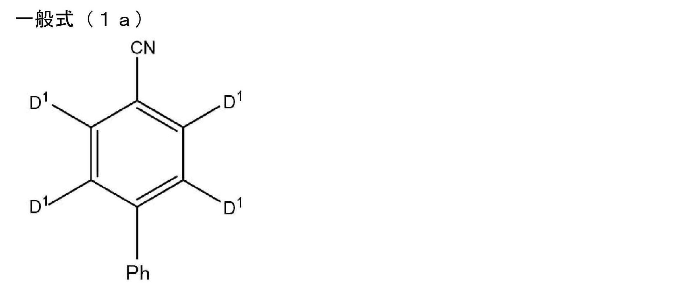
D1の説明の好ましい範囲、具体例については、その置換位置の説明を除いて、上記の一般式(1)のDについての説明と好ましい範囲、具体例を参照することができ、Phの説明と好ましい範囲、具体例については、その置換位置の説明を除いて、上記の一般式(1)のPhについての説明と好ましい範囲、具体例を参照することができる。

D1およびD2は、無置換のカルバゾール-9-イル基であっても、水素原子の少なくとも1つが置換基で置換されたカルバゾール-9-イル基(置換カルバゾール-9-イル基)であってもよい。置換カルバゾール-9-イル基の説明と好ましい範囲、具体例については、上記のDにおける置換カルバゾール-9-イル基についての説明と好ましい範囲、具体例を参照することができる。ただし、一般式(2)のD2は、D1とは異なる置換もしくは無置換のカルバゾール-9-イル基を表す。D1が表す置換もしくは無置換のカルバゾール-9-イル基と、D2が表す置換もしくは無置換のカルバゾール-9-イル基は、置換基の有無、置換基の数、置換基の構造および置換位置のいずれが異なっていてもよい。
2つのPhは各々独立に、アルキル基、アリール基およびこれらが連結した基からなる群より選択される少なくとも1つの基で置換されていてもよいフェニル基を表す。2つのPhは互いに同一であっても異なっていてもよい。Phが表す「アルキル基、アリール基およびこれらが連結した基からなる群より選択される少なくとも1つの基で置換されていてもよいフェニル基」の説明と好ましい範囲、具体例については、上記の一般式(1)のPhが表す「アルキル基、アリール基およびこれらが連結した基からなる群より選択される少なくとも1つの基で置換されていてもよいフェニル基」についての説明と好ましい範囲、具体例を参照することができる。
一般式(2)において、D1、D2およびPhのベンゼン環における置換位置は特に制限されない。例えば、2つのPhの置換位置は、それぞれCN基に対するオルト位、メタ位、パラ位のいずれであってもよく、いずれの場合も、その残りの置換可能位置がD1および2つのD2の置換位置になる。2つのPhの好ましい置換位置として、CN基に対するオルト位およびパラ位を挙げることができる。D2の好ましい置換位置として、CN基に対するメタ位を挙げることができる。

D1、D2、Phの説明については、ベンゼン環における置換位置の説明を除いて、上記の一般式(2)のD1、D2、Phの説明を参照することができる。
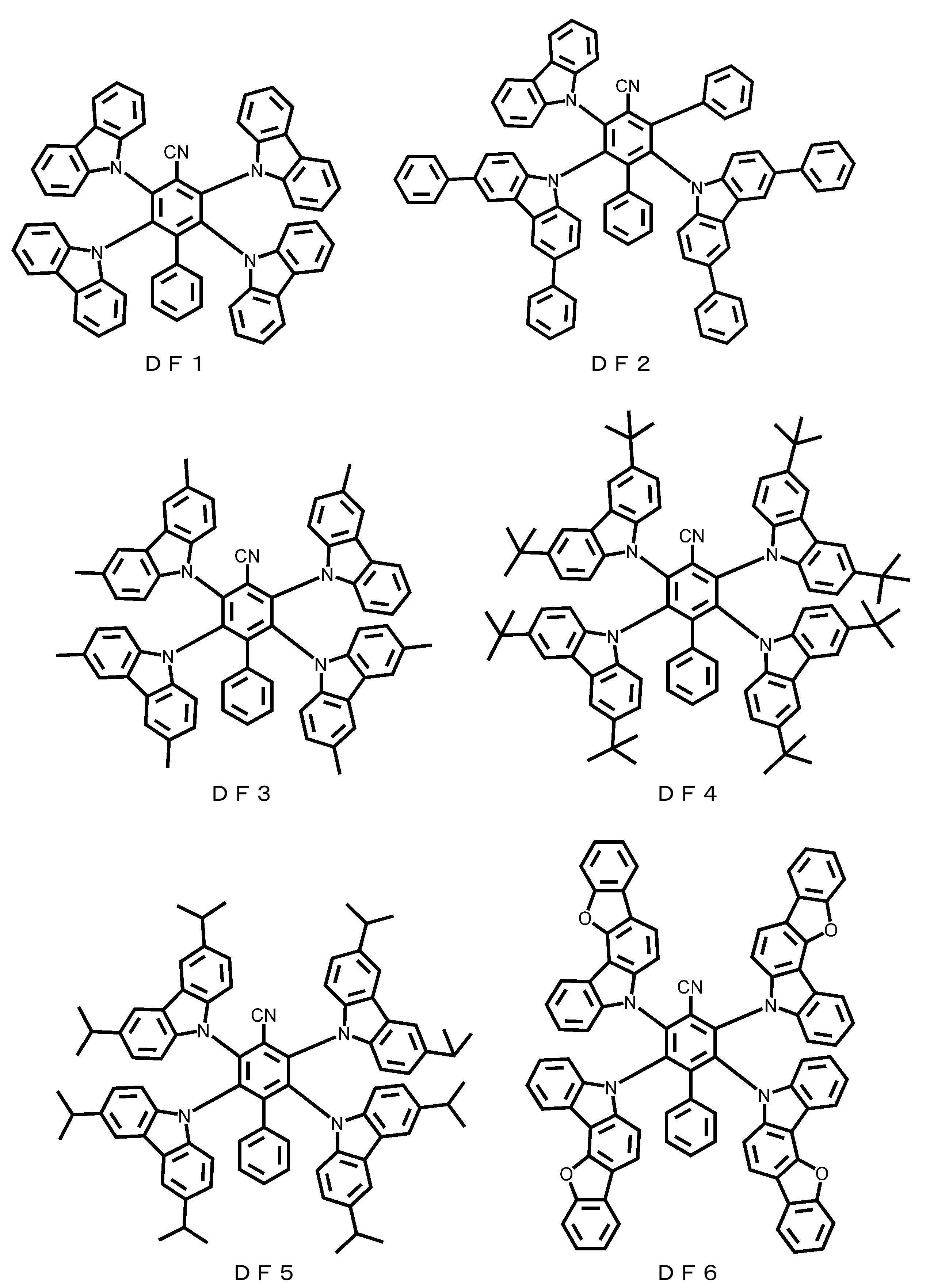


第3有機化合物は多重共鳴型蛍光材料であることが好ましく、多重共鳴型遅延蛍光材料であることがより好ましい。
第3有機化合物は、窒素原子、酸素原子および硫黄原子からなる群より選択される1種以上の原子とホウ素原子との間で多重共鳴する化合物であることが好ましい。
本明細書の一部としてここに引用する、国際公開第2020/039930の段落[0011]~[0032]に記載される一般式で表される化合物や具体的な化合物、および下記式で表される化合物を第3有機化合物として好ましく用いることができる。
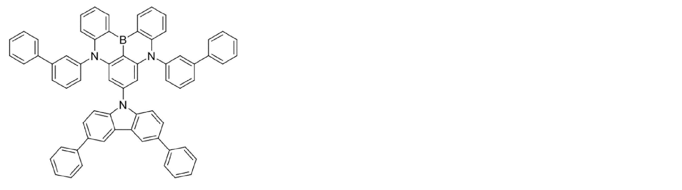
第1有機化合物は、第2有機化合物および第2有機化合物よりも最低励起一重項エネルギーが高い有機化合物であり、例えば公知のホスト材料の中から選択して用いることができる。
以下において、第3有機化合物として用いうる化合物の具体例を例示する。ただし、本発明において用いることができる第3有機化合物は、これらの具体例によって限定的に解釈されるべきものではない。

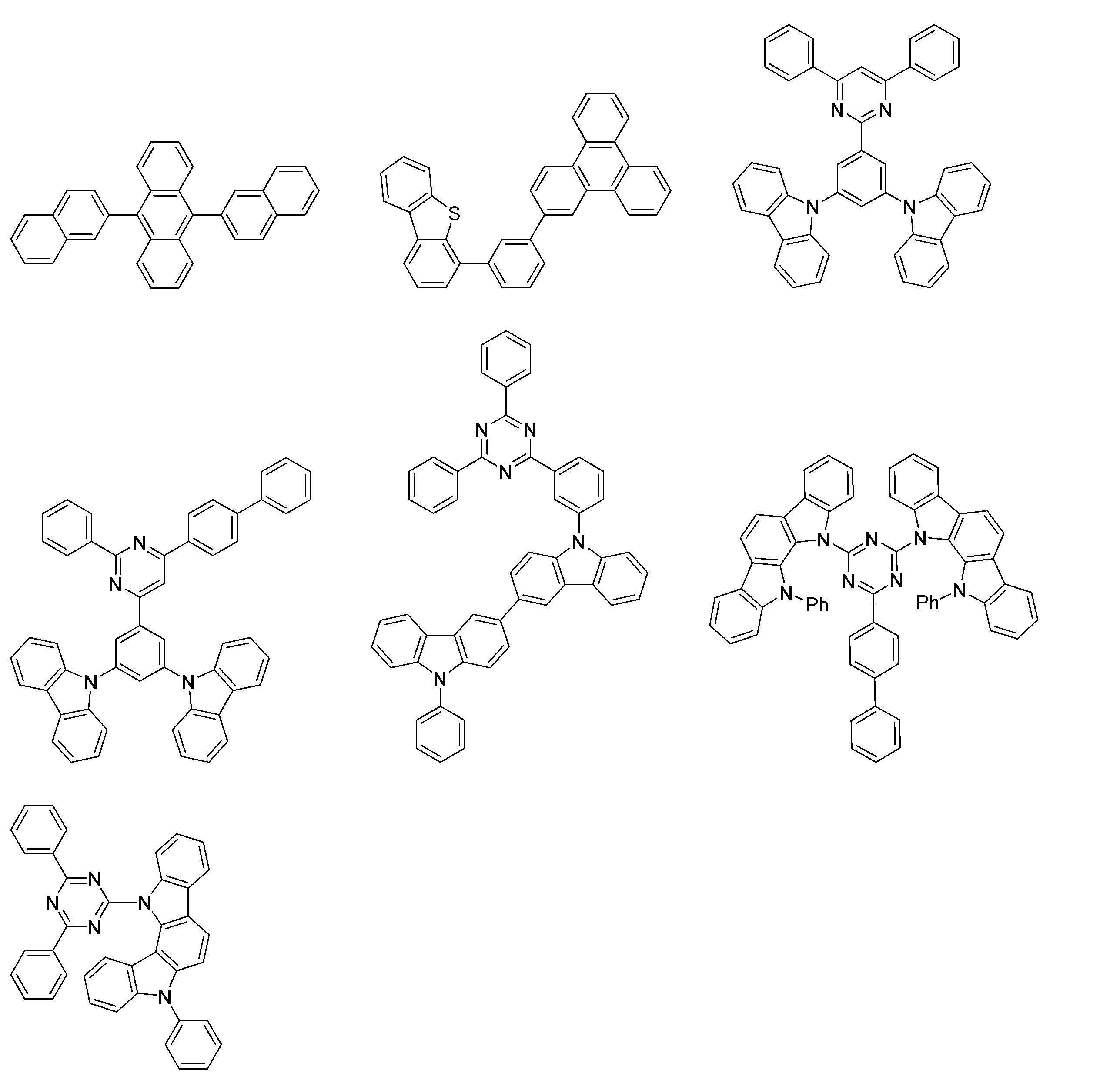
本発明の組成物において、第1有機化合物と第2有機化合物と第3有機化合物の配合比は特に制限されないが、第2有機化合物の含有量は、第1有機化合物の含有量よりも少なく、第3有機化合物の含有量よりも多いこと、すなわち、「第3有機化合物の含有量<第2有機化合物の含有量<第1有機化合物の含有量」の関係を満たすことが好ましい。
具体的には、組成物における第2有機化合物の含有量は、第1有機化合物と第2有機化合物と第3有機化合物の合計量に対して50重量%未満とすることが好ましい。さらに、第2有機化合物の含有量の上限値は、第1有機化合物と第2有機化合物と第3有機化合物の合計量に対して40重量%未満とすることが好ましく、例えば30重量%未満、20重量%未満、10重量%未満とすることもできる。下限値は0.1重量%以上とすることが好ましく、例えば1重量%超、3重量%超とすることもできる。
また、組成物における第3有機化合物の含有量は、第1有機化合物と第2有機化合物と第3有機化合物の合計量に対して0.1重量%以上、1重量%以上とすることもできる。また、組成物における第3有機化合物の含有量は、30重量%以下、20重量%以下、10重量%以下とすることもできる。
本発明の組成物は、第1有機化合物と第2有機化合物と第3有機化合物のみから構成されていてもよいし、その他の成分を含んでいてもよい。
上記のように、本発明の組成物は、特に高効率で高色純度の発光を示し、特に480nm未満の波長範囲で高い色純度が得られる。そのため、本発明の組成物は発光組成物として効果的に用いることができる。本発明の組成物を発光組成物として用いる場合の使用態様は特に制限されないが、例えば組成物を膜状に成形して発光膜として用いる態様や、その発光膜を有機発光素子の発光層として用いる態様、組成物を溶媒に溶解して液状の発光材料として用いる態様などが挙げられる。本発明の組成物を用いた発光膜の構成については、下記の<膜>および<発光膜>の欄の記載を参照することができ、本発明の組成物を発光層に用いた有機発光素子の構成については、下記の<有機発光素子>の欄の記載を参照することができる。
次に、本発明の膜について説明する。
本発明の膜は、本発明の組成物を含むことを特徴とする。
本発明の組成物の説明については、上記の<組成物>の欄の記載を参照することができる。
上記のように、本発明の組成物は、特に高効率で高色純度の発光を示し、特に480nm未満の波長範囲で高い色純度が得られるため、この組成物を含む膜も、その組成物の特性を反映して優れた特性を示す。
ある実施形態では、本発明の組成物を含む膜は、湿式工程で形成することができる。湿式工程では、本発明の組成物を溶解した溶液を面に塗布し、溶媒の除去後にフィルムを形成する。湿式工程として、スピンコート法、スリットコート法、インクジェット法(スプレー法)、グラビア印刷法、オフセット印刷法、フレキソ印刷法を挙げることができるが、これらに限定されるものではない。湿式工程では、本発明の組成物を溶解することができる適切な有機溶媒を選択して用いる。ある実施形態では、組成物に含まれる有機化合物に、有機溶媒に対する溶解性を上げる置換基(例えばアルキル基)を導入することができる。
ある実施形態では、本発明の組成物を含む膜は、乾式工程で形成することができる。ある実施形態では、乾式工程として真空蒸着法を採用することができる、これに限定されるものではない。真空蒸着法を採用する場合は、組成物を構成する各有機化合物を個別の蒸着源から共蒸着させてもよいし、各有機化合物を混合した単一の蒸着源から共蒸着させてもよい。単一の蒸着源を用いる場合は、各有機化合物の粉末を混合した混合粉を用いてもよいし、その混合粉を圧縮した圧縮成形体を用いてもよいし、各有機化合物を加熱溶融して冷却した混合物を用いてもよい。ある実施形態では、単一の蒸着源に含まれる複数の有機化合物の蒸着速度(重量減少速度)が一致ないしほぼ一致する条件で共蒸着を行うことにより、蒸着源に含まれる複数の有機化合物の組成比に対応する組成比の膜を形成することができる。形成される膜の組成比と同じ組成比で複数の有機化合物を混合して蒸着源とすれば、所望の組成比を有する膜を簡便に形成することができる。ある実施形態では、共蒸着される各有機化合物が同じ重量減少率になる温度を特定して、その温度を共蒸着時の温度として採用することができる。
本発明の膜の厚さは、10~100nmであることが好ましく、20~60nmであることがより好ましく、30~50nmであることがさらに好ましい。本発明の膜が多層構成である場合、それぞれの膜の厚さの好ましい範囲が、上記の厚さ範囲であることとする。
上記のように、本発明の膜は、特に高効率で高色純度の発光を示し、特に480nm未満の波長範囲で高い色純度が得られる。そのため、本発明の膜は発光膜として効果的に用いることができる。
本発明の膜の説明については、上記の<膜>の欄の記載を参照することができる。
本発明の発光膜は、有機発光素子の発光層として効果的に用いることができる。本発明の発光膜を発光層として用いた有機発光素子の構成については、下記の<有機発光素子>の欄の記載を参照することができる。
本発明の組成物は、所定の条件を満たす第1有機化合物と第2有機化合物と第3有機化合物を含むことによりTAF機構が働いて、特に高効率で高色純度の発光を示し、特に480nm未満の波長範囲で高い色純度が得られる。そのため、本発明の組成物は、TAF型有機発光素子の発光層の材料として効果的に用いることができ、特に有機エレクトロルミネッセンス素子の発光層の材料として好適である。
ここで、US2020/0168814A1の[0141]~[0169]および[0192]~[0242]に記載される使用例、デバイス、ディスプレイ、スクリーン等の説明は、「発光層」の材料を「本発明の組成物」に書き換えて、その全体を本明細書の一部としてここに引用し、本発明の説明とする。
本発明の組成物の説明については、上記の<組成物>の欄の記載を参照することができる。
素子からの発光の最大成分が第3有機化合物からの蛍光であることは、有機エレクトロルミネッセンス素子の発光スペクトルにおいて、第3有機化合物由来の発光ピークの面積が全発光ピーク面積の50%超であることをもって確認することができる。素子からの発光における第3有機化合物由来の蛍光成分の割合は、60%超であることがより好ましく、70%超であることがさらに好ましく、80%超であることがさらにより好ましく、90%超であることが特に好ましい。第3有機化合物由来の発光ピークの波長(有機エレクトロルミネッセンス素子の発光ピークの波長)は制限されないが、好ましい態様では青色発光領域(400nm~490nm)であり、より好ましい態様では420nm~480nmである。
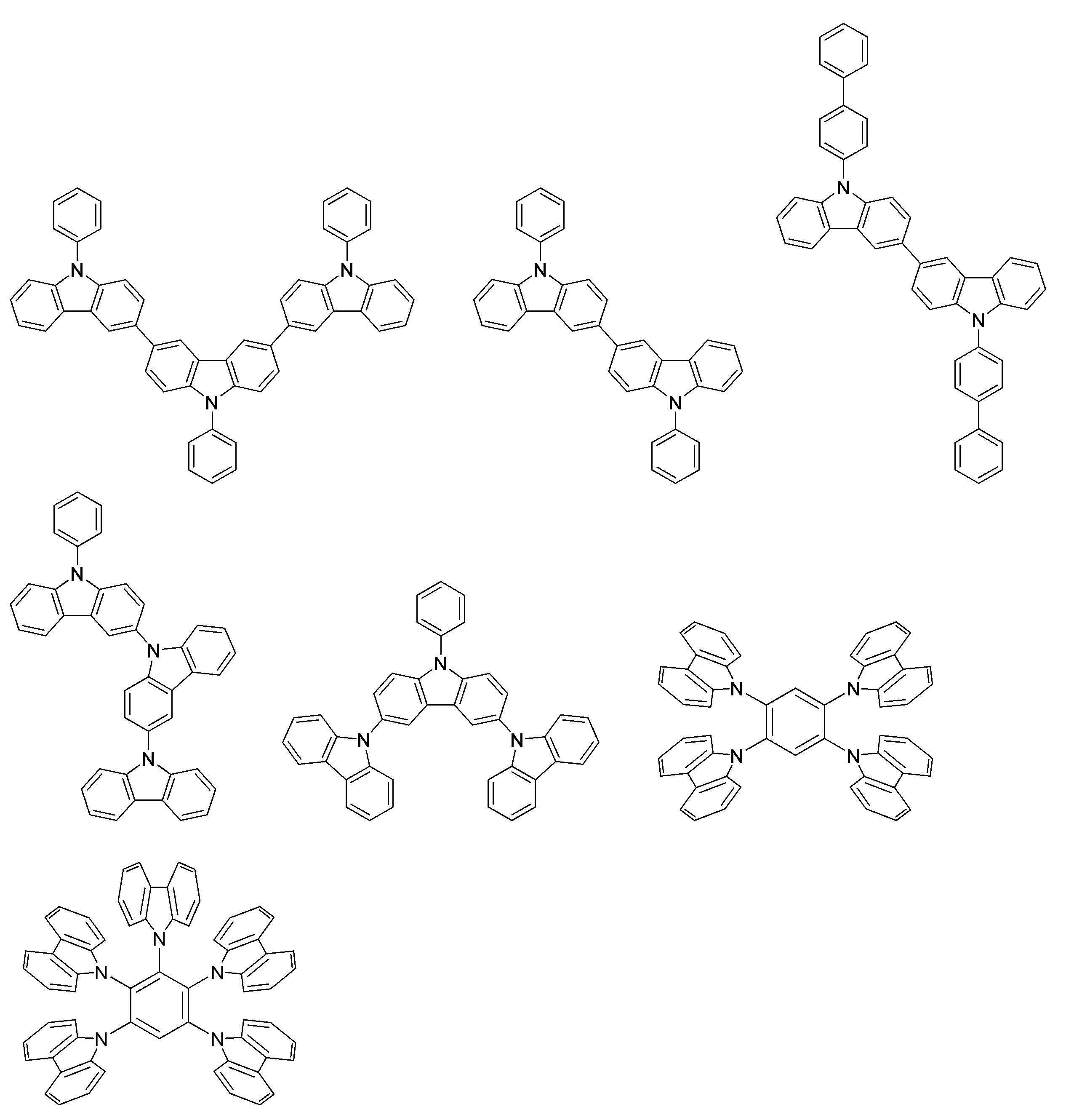
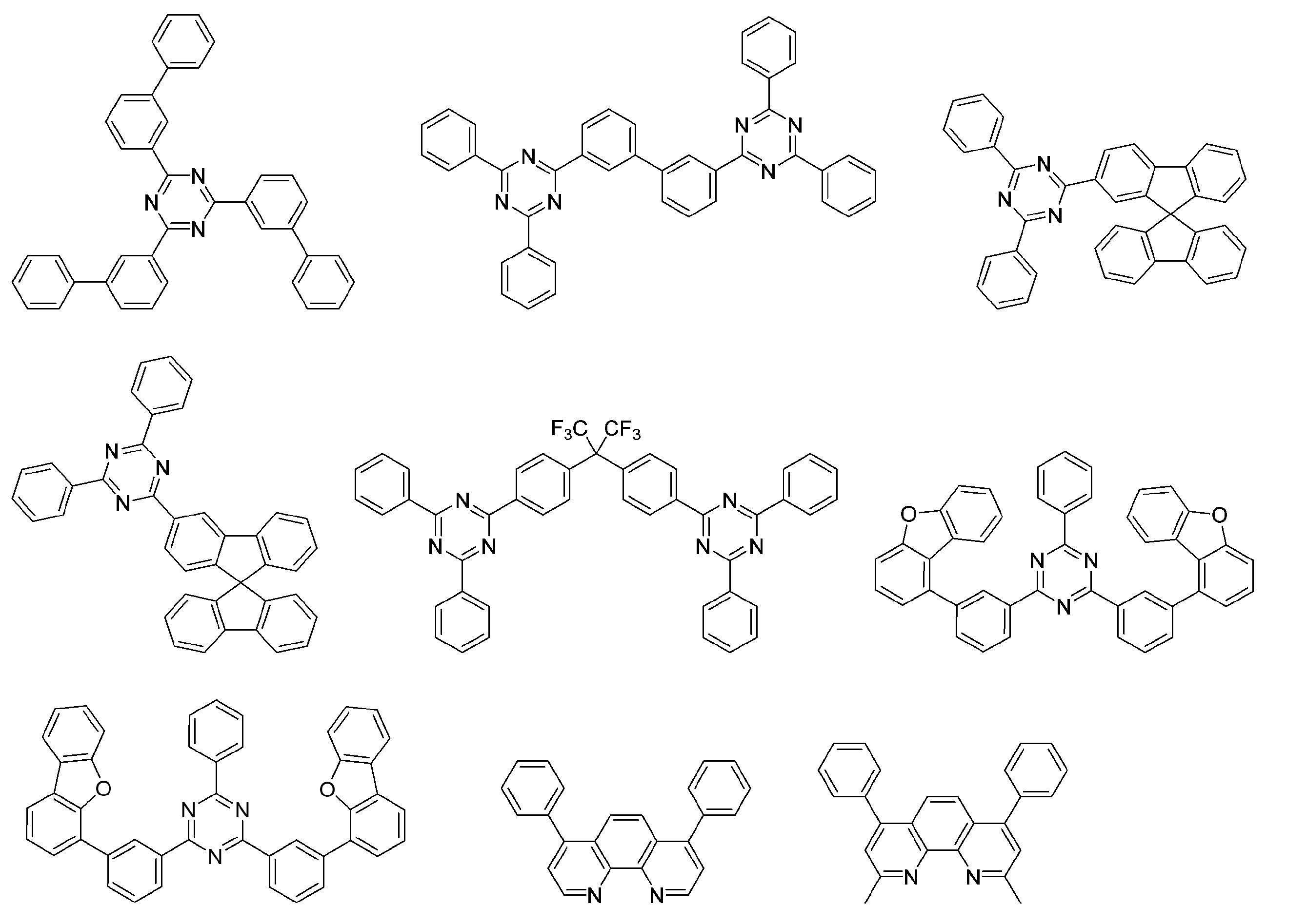
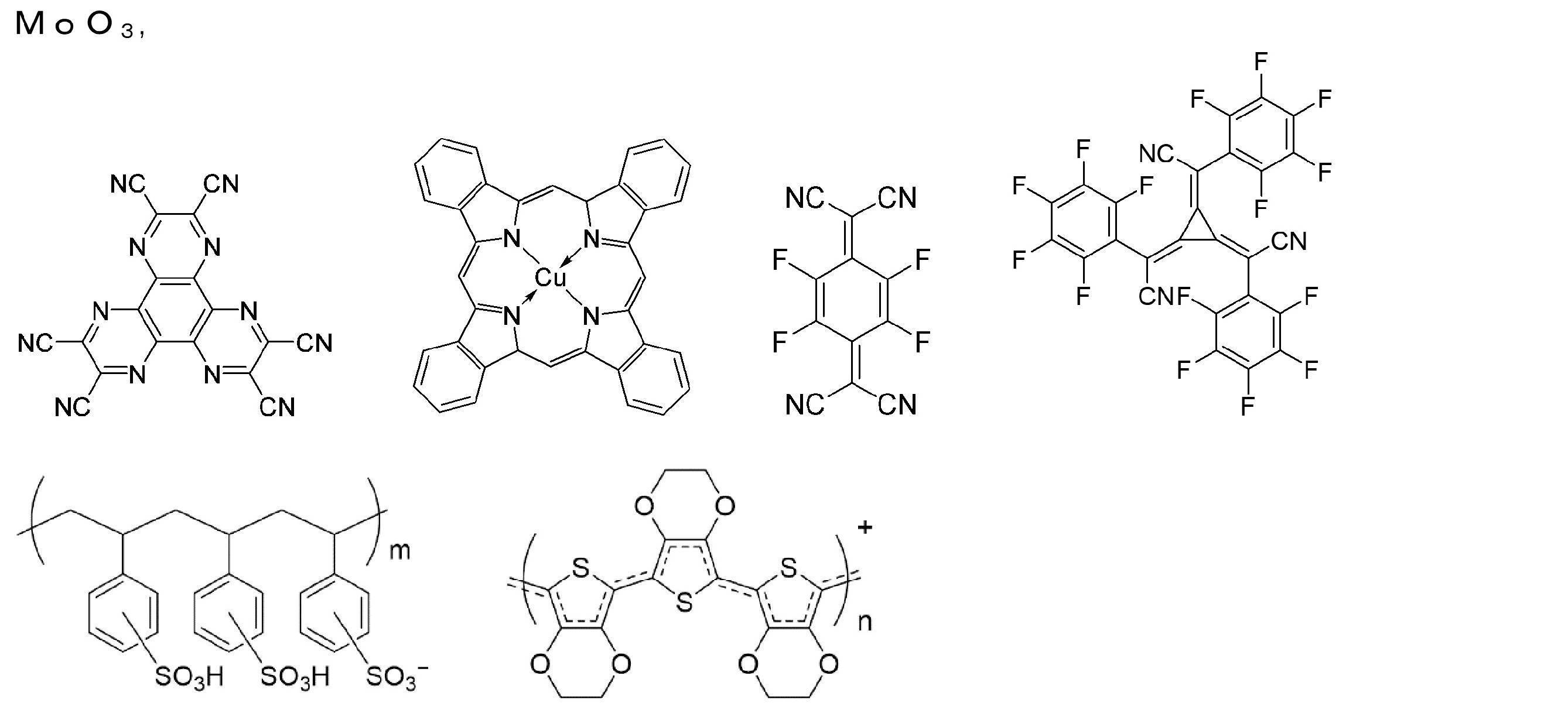


本発明の組成物の設計方法は、上記の条件(a)~(d)を満たすように第1有機化合物と遅延蛍光材料である第2有機化合物と蛍光材料である第3有機化合物を選択することを特徴とする、第1有機化合物と第2有機化合物と第3有機化合物を含む組成物の設計方法である。
本発明の組成物の設計方法では、第1有機化合物と第2有機化合物と第3有機化合物の選択を、上記の条件(f)および(g)も満たすように行うことが好ましく、上記の条件(h)、(i)および(j)の少なくとも1つも満たすように行うことも好ましく、上記の条件(h1)、(i1)および(j1)の全ても満たすように行うことがより好ましい。
すなわち、本発明の組成物の設計方法では、第1有機化合物と第2有機化合物と第3有機化合物の選択を、上記の条件(a)~(d)を満たすように行えばよく、さらに、条件(f)および(g)も満たすか、条件(h)、(i)および(j)の少なくとも1つも満たすように行うことが好ましく、条件(f)および(g)も満たし、且つ、条件(h)、(i)および(j)の少なくとも1つも満たすように行うことがより好ましく、条件(f)および(g)も満たし、且つ、条件(h1)、(i1)および(j1)の全ても満たすように行うことが特に好ましい。
条件(a)~(d)、(f)~(j)、(h1)~(j1)の説明については、上記の<組成物>の欄の記載を参照することができる。
上記のように、条件(a)~(d)を満たす有機化合物の組成物、好ましくは、条件(a)~(d)、および、条件(f)~(j)、(h1)~(j1)を満たす有機化合物の組成物は、特に高効率で高色純の発光を示し、特に480nm未満の波長範囲で高色純度が得られる。また、条件(a)~(d)、(f)~(j)および(h1)~(j1)は、数値の大小関係で示された客観的な指標であるため、条件を満たすものであるか否かを明確に判別することができる。そのため、条件(a)~(d)、条件(f)~(j)、(h1)~(j1)を満たすように、第1有機化合物と第2有機化合物と第3有機化合物を選択することにより、上記のような特性を示す組成物を確実に実現することができる。
ここで、第1有機化合物、第2有機化合物および第3有機化合物の選択対象となる母集団には、上記の[第1有機化合物]、[第2有機化合物]および[第3有機化合物]の欄に例示した化合物群を用いることができる。ただし、本発明の設計方法で用いる選択対象は、これらの化合物例によって限定的に解釈されるべきものではない。
本発明のプログラムは、本発明の組成物の設計方法を実施するためのプログラムである。
本発明の組成物の設計方法の説明については、上記の<組成物の設計方法>の欄の記載を参照することができる。
本発明のプログラムは、例えば第1有機化合物として用いうる化合物群のES1(1)を蓄積したデータベース、第2有機化合物として用いうる化合物群のES1(2)、λE EM(2)およびλP EM(2)を蓄積したデータベース、第3有機化合物として用いうる化合物群のES1(3)、λP AB(3)およびλP EM(3)を蓄積したデータベースを参照して、条件(a)~(d)を満たす第1有機化合物と第2有機化合物と第3有機化合物の組み合わせを選定するステップを有する。
第2有機化合物のデータベースには、その化合物群のLUMO(2)とHOMO(2)も蓄積し、第3有機化合物のデータベースには、その化合物群のLUMO(3)とHOMO(3)も蓄積して、上記のステップにおいて、これらのデータも参照して、条件(a)~(d)とともに、条件(f)および(g)を満たす第1有機化合物と第2有機化合物と第3有機化合物の組み合わせを選定することが好ましい。
また、本発明のプログラムは、上記のステップで選定した第2有機化合物と第3有機化合物の組み合わせについて、R0(2-3)、r(2-3)およびkFRET(2-3)の少なくとも1つを計算するステップと、その組み合わせの中から、条件(h)~(j)の少なくとも1つを満たすものを選択するステップを有することも好ましい。
本発明のプログラムの処理手順例を図1を参照しながら説明する。好ましいプログラムの一態様では、図1に示すようにまず第1有機化合物、第2有機化合物および第3有機化合物の組み合わせを1つ以上想定し(S1)、その各組み合わせについて条件(a)~(d)を満たすか否かを判定する(S2)。その後、さらに他の組み合わせについても判定したい場合は、ステップS1とステップS2を1サイクル以上繰り返す(S3)。判定結果についてはディスプレイに表示したり、印刷したりして出力することができる。その判定結果は、ステップS1とステップS2のサイクルごとに出力してもよいし、すべてのサイクルが終了した後にまとめて出力してもよい。ステップS3では、さらにサイクルを繰り返すか否かの判断をサブプログラムにより行ってもよい。例えば、条件(a)~(d)のすべてを満たす組み合わせが特定の個数以上見いだされるまでサイクルを繰り返す指令を出すサブプログラムを用いることができる。サイクルを1回以上繰り返す場合、ステップS1では前に想定した組み合わせとは異なる組み合わせを新たに想定する。このとき、第1有機化合物、第2有機化合物および第3有機化合物のいずれか1種だけを変更してもよいし、いずれか2種を変更してもよいし、3種のすべてを変更してもよい。また、候補となる第1有機化合物、第2有機化合物および第3有機化合物をあらかじめ読み込ませておき、それらの候補化合物の組み合わせを順に出力するサブプログラムをステップS1で使用してもよい。その他、当業者に自明な改変を適宜行うことができる。
下記の各実施例および各比較例で使用した化合物を以下に示す。各実施例では、ホスト材料の欄に示した化合物H1が第1有機化合物に対応し、遅延蛍光材料の欄に示した化合物DF1またはDF2が第2有機化合物に対応し、蛍光材料の欄に示した化合物F1が第3有機化合物に対応する。
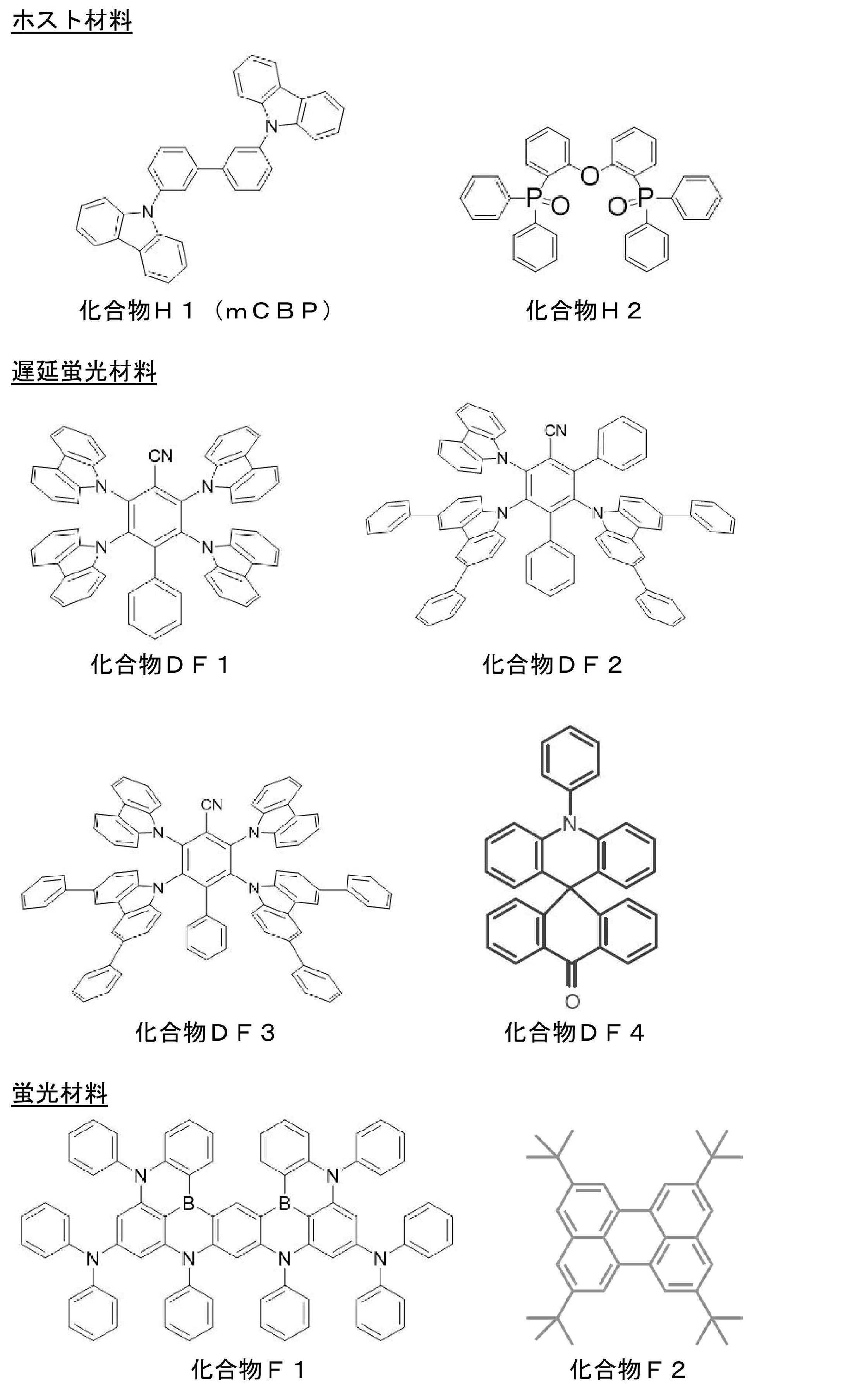




(実施例1) 組成物1の薄膜の作製
真空蒸着法を用い、真空度1×10⁻⁶Paの条件で、石英基板上に、化合物H1と化合物DF1と化合物F1とを異なる蒸着源から蒸着して40nm厚の薄膜(組成物1)を形成した。このとき、各化合物の組成比(化合物H1:化合物DF1:化合物F1)は69:30:1.0(重量比)とした。
化合物DF1の代わりに化合物DF2を用いること以外は、実施例1と同様にして薄膜(組成物2)を形成した。
化合物DF1の代わりに化合物DF3を用いること以外は、実施例1と同様にして薄膜(比較組成物1)を形成した。
化合物H1の代わりに化合物H2を用い、化合物DF1の代わりに化合物DF4を用い、化合物F1の代わりに化合物F2を用いること以外は、実施例1と同様にして薄膜(比較組成物2)を形成した。
実施例1、2および比較例1で作製した各薄膜について、365nm励起光で測定した発光スペクトルを図2に示し、発光極大波長、フォトルミネッセンス量子収率(PLQY)、FW0.3Mおよび、CIE色度座標の測定結果を表5に示す。

また、条件(b)を満たさない比較組成物2の薄膜についても、365nm励起光による発光スペクトルを測定したところ、裾が広がったブロードなピーク形状であった。
このことから、条件(a)~(d)を満たす3種類の有機化合物を用いて組成物を構成することにより、条件(b)を満たさない組成物に比べて色純度が大きく改善されることがわかった。
下記の実施例3~5および比較例3、4では図3に示す積層構造を有するボトムエミッション型の有機エレクトロルミネッセンス素子を作製した。
(実施例3) 組成物1を発光層に用いた有機エレクトロルミネッセンス素子の作製
膜厚50nmのインジウム・スズ酸化物(ITO)からなる陽極2が形成されたガラス基板1上に、各薄膜を真空蒸着法にて、真空度1×10-6Paで積層した。まず、ITO上にHATCNを10nmの厚さに蒸着して正孔注入層3を形成した。続いて、α-NPDを35nmの厚さに蒸着して第1正孔輸送層4を形成し、その上に、TrisPCzを10nmの厚さに蒸着して第2正孔輸送層5を形成した。さらに、mCBPを5nmの厚さに蒸着して電子ブロック層6を形成した。次に、組成物1からなる発光層を形成した。具体的には、化合物H1と化合物DF1と化合物F1を異なる蒸着源から共蒸着し、40nmの厚さの層を形成して発光層7とした。このとき、各化合物の組成比(化合物H1:化合物DF1:化合物F1)は69:30:1.0(重量比)とした。次に、化合物aを10nmの厚さに蒸着して正孔ブロック層8を形成し、その上に、化合物aとLiqを異なる蒸着源から共蒸着して、30nmの厚さの正孔輸送層9を形成した。このとき、各化合物の組成比(化合物a:Liq)は70:30(重量比)とした。続いて、Liqを2nmの厚さに蒸着して電子注入層10を形成し、その上に、Alを100nmの厚さに蒸着して陰極11を形成した。以上の工程で、組成物1を発光層に用いた有機エレクトロルミネッセンス素子(EL素子1)を作製した。
発光層の組成比(化合物H1:化合物DF1:化合物F1)を69.5:30:0.5(重量比)としたこと以外は、実施例3と同様にして有機エレクトロルミネッセンス素子(EL素子2)を作製した。
また、これとは別に、発光層の組成比(化合物H1:化合物DF1:化合物F1)を68:30:2.0(重量比)としたこと以外は、実施例3と同様にして有機エレクトロルミネッセンス素子(EL素子3)を作製した。
化合物F1を用いずに、化合物H1:化合物DF1を70:30(重量比)として発光層を形成したこと以外は、実施例3と同様にして有機エレクトロルミネッセンス素子(比較EL素子1)を作製した。
組成物1の代わりに比較組成物1の組成で発光層を形成したこと以外は、実施例3と同様にして有機エレクトロルミネッセンス素子(比較EL素子2)を作製した。
実施例3~5および比較例3で作製した各EL素子について測定した発光スペクトルを図4に示す。図4中、括弧内の数値は発光層における化合物F1の濃度を示す。また、実施例3~5および比較例3、4で作製した各EL素子について、1000cd/m2で測定した駆動電圧、外部量子効率(EQE)、CIE色度座標および発光のピークトップ波長(発光極大波長)を表6に示す。

このことから、条件(a)~(d)を満たす3種類の有機化合物を用いて発光層を構成することにより、第3有機化合物を用いない素子に比べて効率と色純度が向上し、3種類の有機化合物を用いているが条件(b)を満たさない素子に比べて色純度が向上することがわかった。
実施例3で作製したボトムエミッション型のEL素子1、EL素子1の組成物1の代わりに組成物2を発光層に用いるEL素子4、および比較例4で作製したボトムエミッション型の比較EL素子2について、計算による光学シミュレーションを行って素子特性を評価した。また、組成物1を発光層に用いるトップエミッション型のEL素子5、組成物2を発光層に用いるトップエミッション型のEL素子6、比較組成物1を発光層に用いるトップエミッション型の比較EL素子3についても、計算による光学シミュレーションを行って素子特性を評価した。その結果を表7に示す。
トップエミッション型のEL素子(EL素子5、6、比較EL素子3)は、ガラス基板の上に、下記の層構成が積層されたトップエミッション型有機エレクトロルミネッセンス素子である。下記層構成において、「/」は層同士の間の境界を示し、丸括弧内の数値は各層の厚さである。また、「APC反射層」は、Ag:98重量%、Pd:1重量%、Cu:1重量%の組成を有する合金層であり、APC反射層側がガラス基板側に配置していることとする。「組成物」は発光層を構成する組成物であり、EL素子5では組成物1、EL素子6では組成物2、比較EL素子3では比較組成物1である。
APC反射層(150nm)/ITO陽極(10nm)/HATCNの正孔注入層(10nm)/α-NPDの第1正孔輸送層(35nm)/TrisPCzの第2正孔輸送層(10nm)/mCBPの電子ブロック層(5nm)/組成物からなる発光層(40nm)/化合物aの正孔ブロック層(10nm)/化合物a(70重量%):Liq(30重量%)の電子輸送層(30nm)/Liqの電子注入層(2nm)/MgAg陰極(15nm)/α-NPD(105nm)

以下において、発光層以外で用いた有機エレクトロルミネッセンス素子の材料を示す。

2 陽極
3 正孔注入層
4 第1正孔輸送層
5 第2正孔輸送層
6 電子ブロック層
7 発光層
8 正孔ブロック層
9 正孔輸送層
10 陰極
Claims (25)
- 下記条件(a)~(d)を満たす第1有機化合物と遅延蛍光材料である第2有機化合物と蛍光材料である第3有機化合物を含む組成物。
条件(a) ES1(1)> ES1(2)> ES1(3)
条件(b) λE EM(2)< λP AB(3)-10nm
条件(c) λP EM(3)< λP EM(2)
条件(d) λP EM(3)< 480nm
(上式において、
ES1(1)は前記第1有機化合物の最低励起一重項エネルギー、
ES1(2)は前記第2有機化合物の最低励起一重項エネルギー、
ES1(3)は前記第3有機化合物の最低励起一重項エネルギー、
λE EM(2)は前記第2有機化合物の短波長側の発光波長(単位nm)、
λP AB(3)は前記第3有機化合物の吸収スペクトルの最も長波長側のピークトップの波長(単位nm)、
λP EM(2)は前記第2有機化合物の発光スペクトルのピークトップの波長、
λP EM(3)は前記第3有機化合物の発光スペクトルのピークトップの波長
を表す。) - 下記条件(e)を満たす、請求項1に記載の組成物。
条件(e) FW0.3M < 40nm
(上式において、FW0.3M は前記組成物の発光スペクトルの発光ピークに対する相対強度が30%におけるスペクトル幅を表す。) - 下記条件(e1)を満たす、請求項2に記載の組成物。
条件(e1) FW0.3M < 32nm - 下記条件(f)および(g)を満たす、請求項1~3のいずれか1項に記載の組成物。
条件(f) LUMO(2)≦ LUMO(3)
条件(g) HOMO(2)≦ HOMO(3)
(上式において、
LUMO(2)は前記第2有機化合物のLUMOのエネルギー、
LUMO(3)は前記第3有機化合物のLUMOのエネルギー、
HOMO(2)は前記第2有機化合物のHOMOのエネルギー、
HOMO(3)は前記第3有機化合物のHOMOのエネルギー
を表す。) - 下記条件(h)を満たす、請求項1~4のいずれか1項に記載の組成物。
条件(h) R0(2-3)> 6.5nm
(上式において、R0(2-3)は、前記第2有機化合物と前記第3有機化合物との間のフェルスター半径を表す。) - 下記条件(i)を満たす、請求項1~5のいずれか1項に記載の組成物。
条件(i) r(2-3)< 3.91nm
(上式において、r(2-3)は、前記第2有機化合物と前記第3有機化合物との間の分子間距離を表す。) - 下記条件(j)を満たす、請求項1~6のいずれか1項に記載の組成物。
条件(j) kFRET(2-3)> 1.5×10⁹s-1
(上式において、kFRET(2-3)は、前記第2有機化合物と前記第3有機化合物との間のフェルスターエネルギー移動速度定数を表す。) - 下記条件(h1)、(i1)および(j1)を満たす、請求項1~4のいずれか1項に記載の組成物。
条件(h1) R0(2-3)≧ 7.3nm
条件(i1) r(2-3)≦ 3.71nm
条件(j1) kFRET(2-3)≧ 6.1×10⁹s-1
(上式において、
R0(2-3)は、前記第2有機化合物と前記第3有機化合物との間のフェルスター半径、
r(2-3)は、前記第2有機化合物と前記第3有機化合物との間の分子間距離、
kFRET(2-3)は、前記第2有機化合物と前記第3有機化合物との間のフェルスターエネルギー移動速度定数
を表す。) - 前記有機第2化合物が下記一般式(1)で表される構造を有する、請求項1~8のいずれか1項に記載の組成物。

- 前記有機第2化合物が下記一般式(1a)で表される構造を有する、請求項9に記載の組成物。
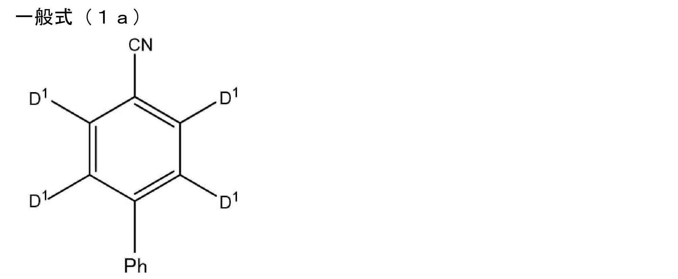
- 前記有機第2化合物が下記一般式(2)で表される構造を有する、請求項1~8のいずれか1項に記載の組成物。
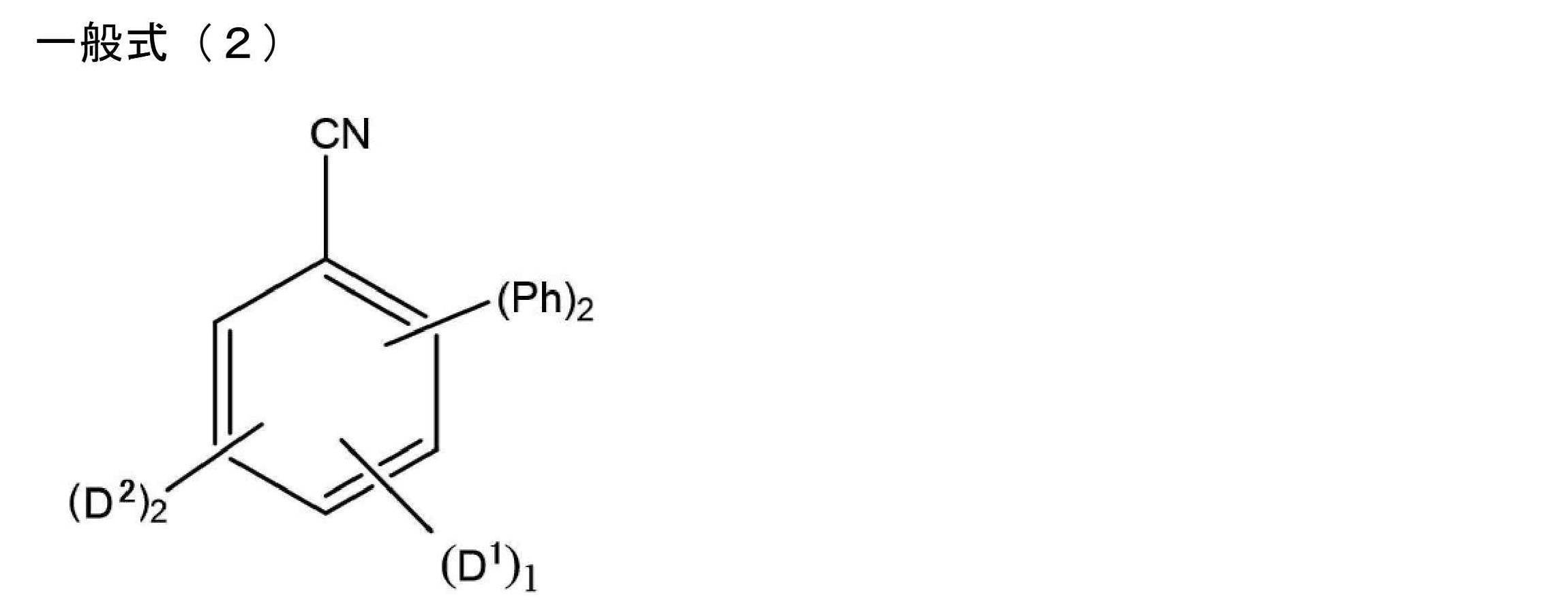
- 前記有機第2化合物が下記一般式(2a)で表される構造を有する、請求項11に記載の組成物。

- D、D1およびD2が、各々独立に下記D1~D37のいずれかで表される構造を有する、請求項9~12のいずれか1項に記載の組成物。
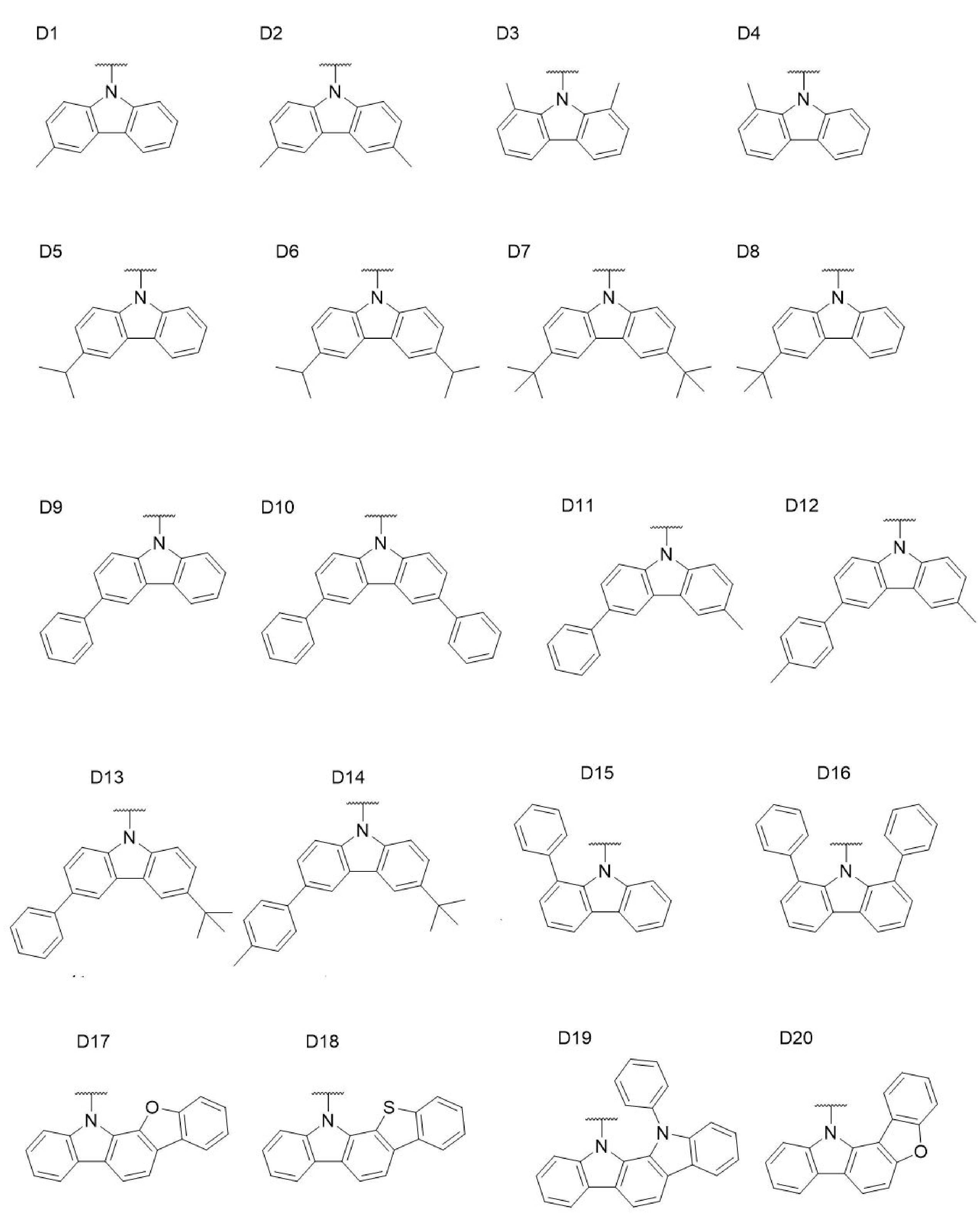
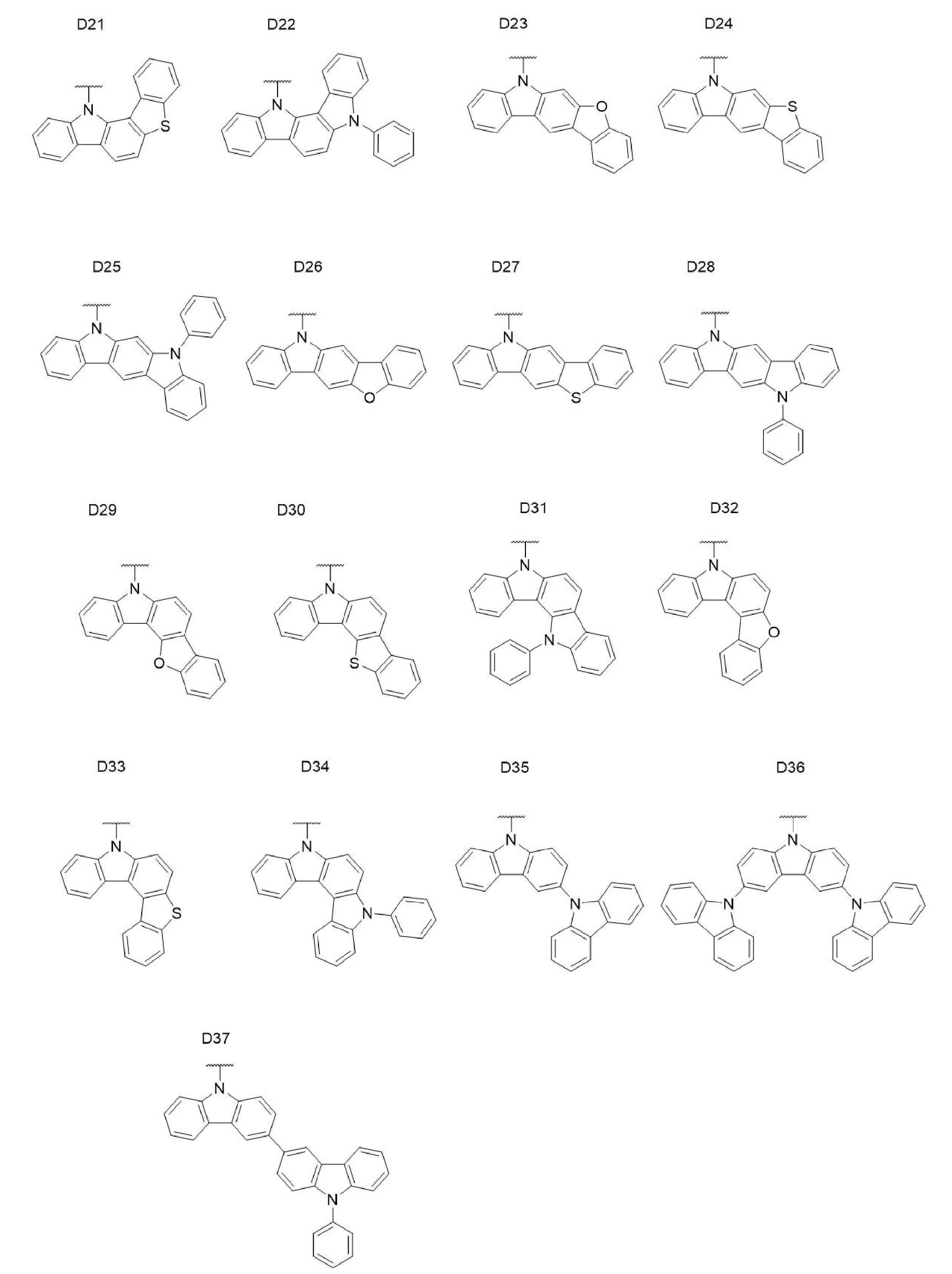
- 請求項1~13のいずれか1項に記載の組成物の発光組成物としての使用。
- 請求項1~13のいずれか1項に記載の組成物の発光組成物を含む膜。
- 請求項15に記載の膜の発光膜としての使用。
- 陽極、陰極、および前記陽極と前記陰極の間に発光層を含む少なくとも一層の有機層を有する有機エレクトロルミネッセンス素子であって、
前記発光層は、請求項1~13のいずれか1項に記載の組成物を含み、
前記素子からの発光の最大成分は前記第3有機化合物からの蛍光である、有機エレクトロルミネッセンス素子。 - トップエミッション型である、請求項17に記載の有機エレクトロルミネッセンス素子。
- 下記条件(a)~(d)を満たすように第1有機化合物と遅延蛍光材料である第2有機化合物と蛍光材料である第3有機化合物を選択することを特徴とする、第1有機化合物と第2有機化合物と第3有機化合物を含む組成物の設計方法。
条件(a) ES1(1)> ES1(2)> ES1(3)
条件(b) λE EM(2)< λP AB(3)-10nm
条件(c) λP EM(3)< λP EM(2)
条件(d) λP EM(3)< 480nm
(上式において、
ES1(1)は前記第1有機化合物の最低励起一重項エネルギー、
ES1(2)は前記第2有機化合物の最低励起一重項エネルギー、
ES1(3)は前記第3有機化合物の最低励起一重項エネルギー、
λE EM(2)は前記第2有機化合物の短波長側の発光波長(単位nm)、
λP AB(3)は前記第3有機化合物の吸収スペクトルの最も長波長側のピークトップの波長(単位nm)、
λP EM(2)は前記第2有機化合物の発光スペクトルのピークトップの波長、
λP EM(3)は前記第3有機化合物の発光スペクトルのピークトップの波長
を表す。) - 前記選択を、下記条件(f)および(g)も満たすように行う、請求項19に記載の組成物の設計方法。
条件(f) LUMO(2)≦ LUMO(3)
条件(g) HOMO(2)≦ HOMO(3)
(上式において、
LUMO(2)は前記第2有機化合物のLUMOのエネルギー、
LUMO(3)は前記第3有機化合物のLUMOのエネルギー、
HOMO(2)は前記第2有機化合物のHOMOのエネルギー、
HOMO(3)は前記第3有機化合物のHOMOのエネルギー
を表す。) - 前記選択を、下記条件(h)も満たすように行う、請求項19または20に記載の組成物の設計方法。
条件(h) R0(2-3)> 6.5nm
(上式において、R0(2-3)は、前記第2有機化合物と前記第3有機化合物との間のフェルスター半径を表す。) - 前記選択を、下記条件(i)も満たすように行う、請求項19~21のいずれか1項に記載の組成物の設計方法。
条件(i) r(2-3)< 3.91nm
(上式において、r(2-3)は、前記第2有機化合物と前記第3有機化合物との間の分子間距離を表す。) - 前記選択を、下記条件(j)も満たすように行う、請求項19~22のいずれか1項に記載の組成物の設計方法。
条件(j) kFRET(2-3)> 1.5×10⁹s-1
(上式において、kFRET(2-3)は、前記第2有機化合物と前記第3有機化合物との間のフェルスターエネルギー移動速度定数を表す。) - 前記選択を、下記条件(h1)、(i1)および(j1)も満たすように行う、請求項19に記載の組成物の設計方法。
条件(h1) R0(2-3)≧ 7.3nm
条件(i1) r(2-3)≦ 3.71nm
条件(j1) kFRET(2-3)≧ 6.1×10⁹s-1
(上式において、
R0(2-3)は、前記第2有機化合物と前記第3有機化合物との間のフェルスター半径、
r(2-3)は、前記第2有機化合物と前記第3有機化合物との間の分子間距離、
kFRET(2-3)は、前記第2有機化合物と前記第3有機化合物との間のフェルスターエネルギー移動速度定数
を表す。) - 請求項19~24のいずれか1項に記載の組成物の設計方法を実施するためのプログラム。
Priority Applications (4)
| Application Number | Priority Date | Filing Date | Title |
|---|---|---|---|
| CN202280021215.4A CN117121651A (zh) | 2021-03-16 | 2022-03-14 | 组合物、将该组合物作为发光组合物的用途、膜、将该膜作为发光膜的用途、有机电致发光元件、组合物的设计方法及用于实施该设计方法的程序 |
| EP22771349.2A EP4310930A4 (en) | 2021-03-16 | 2022-03-14 | COMPOSITION, USE OF SAID COMPOSITION AS ELECTROLUMINESCENT COMPOSITION, FILM, USE OF SAID FILM AS ELECTROLUMINESCENT FILM, ORGANIC ELECTROLUMINESCENT ELEMENT, METHOD FOR DESIGNING THE COMPOSITION AND PROGRAM FOR IMPLEMENTING SAID DESIGN METHOD |
| US18/550,531 US20240188436A1 (en) | 2021-03-16 | 2022-03-14 | Composition, use of said composition as light-emitting composition, film, use of said film as light-emitting film, organic electroluminescent element, method for designing composition, and program for implementing said design method |
| KR1020237031682A KR20230156073A (ko) | 2021-03-16 | 2022-03-14 | 조성물, 그 조성물의 발광 조성물로서의 사용, 막, 그 막의 발광막으로서의 사용, 유기 일렉트로 루미네선스 소자, 조성물의 설계 방법 및 그 설계 방법을 실시하기 위한 프로그램 |
Applications Claiming Priority (2)
| Application Number | Priority Date | Filing Date | Title |
|---|---|---|---|
| JP2021-042437 | 2021-03-16 | ||
| JP2021042437A JP7674727B2 (ja) | 2021-03-16 | 2021-03-16 | 組成物、その組成物の発光組成物としての使用、膜、その膜の発光膜としての使用、有機エレクトロルミネッセンス素子、組成物の設計方法およびその設計方法を実施するためのプログラム |
Publications (1)
| Publication Number | Publication Date |
|---|---|
| WO2022196603A1 true WO2022196603A1 (ja) | 2022-09-22 |
Family
ID=83320363
Family Applications (1)
| Application Number | Title | Priority Date | Filing Date |
|---|---|---|---|
| PCT/JP2022/011169 Ceased WO2022196603A1 (ja) | 2021-03-16 | 2022-03-14 | 組成物、その組成物の発光組成物としての使用、膜、その膜の発光膜としての使用、有機エレクトロルミネッセンス素子、組成物の設計方法およびその設計方法を実施するためのプログラム |
Country Status (6)
| Country | Link |
|---|---|
| US (1) | US20240188436A1 (ja) |
| EP (1) | EP4310930A4 (ja) |
| JP (1) | JP7674727B2 (ja) |
| KR (1) | KR20230156073A (ja) |
| CN (1) | CN117121651A (ja) |
| WO (1) | WO2022196603A1 (ja) |
Cited By (1)
| Publication number | Priority date | Publication date | Assignee | Title |
|---|---|---|---|---|
| WO2024143996A1 (ko) * | 2022-12-28 | 2024-07-04 | 덕산네오룩스 주식회사 | 유기전기 소자용 화합물을 이용한 유기전기소자 및 그 전자 장치 |
Families Citing this family (1)
| Publication number | Priority date | Publication date | Assignee | Title |
|---|---|---|---|---|
| US20230091551A1 (en) * | 2021-09-23 | 2023-03-23 | The Regents Of The University Of Michigan | White organic light emitting device with stable spectrum employing transport barrier layers |
Citations (5)
| Publication number | Priority date | Publication date | Assignee | Title |
|---|---|---|---|---|
| WO2019009307A1 (ja) * | 2017-07-03 | 2019-01-10 | 三菱ケミカル株式会社 | Oled素子形成用組成物及びoled素子 |
| JP2020031162A (ja) * | 2018-08-23 | 2020-02-27 | 国立大学法人九州大学 | 有機エレクトロルミネッセンス素子 |
| WO2020039930A1 (ja) | 2018-08-23 | 2020-02-27 | 国立大学法人九州大学 | 有機発光素子、組成物および膜 |
| WO2020067143A1 (ja) * | 2018-09-25 | 2020-04-02 | 国立大学法人京都大学 | 化合物、発光材料、遅延蛍光体、有機発光素子、酸素センサー、分子の設計方法およびプログラム |
| US20200168814A1 (en) | 2018-11-27 | 2020-05-28 | Kyulux, Inc. | Composition of matter for use in organic light-emitting diodes |
Family Cites Families (2)
| Publication number | Priority date | Publication date | Assignee | Title |
|---|---|---|---|---|
| CN119277888A (zh) * | 2018-11-30 | 2025-01-07 | 九州有机光材股份有限公司 | 有机发光元件 |
| JP7515098B2 (ja) * | 2019-02-13 | 2024-07-12 | 学校法人関西学院 | 多環芳香族化合物およびその多量体 |
-
2021
- 2021-03-16 JP JP2021042437A patent/JP7674727B2/ja active Active
-
2022
- 2022-03-14 US US18/550,531 patent/US20240188436A1/en active Pending
- 2022-03-14 CN CN202280021215.4A patent/CN117121651A/zh active Pending
- 2022-03-14 WO PCT/JP2022/011169 patent/WO2022196603A1/ja not_active Ceased
- 2022-03-14 EP EP22771349.2A patent/EP4310930A4/en active Pending
- 2022-03-14 KR KR1020237031682A patent/KR20230156073A/ko active Pending
Patent Citations (5)
| Publication number | Priority date | Publication date | Assignee | Title |
|---|---|---|---|---|
| WO2019009307A1 (ja) * | 2017-07-03 | 2019-01-10 | 三菱ケミカル株式会社 | Oled素子形成用組成物及びoled素子 |
| JP2020031162A (ja) * | 2018-08-23 | 2020-02-27 | 国立大学法人九州大学 | 有機エレクトロルミネッセンス素子 |
| WO2020039930A1 (ja) | 2018-08-23 | 2020-02-27 | 国立大学法人九州大学 | 有機発光素子、組成物および膜 |
| WO2020067143A1 (ja) * | 2018-09-25 | 2020-04-02 | 国立大学法人京都大学 | 化合物、発光材料、遅延蛍光体、有機発光素子、酸素センサー、分子の設計方法およびプログラム |
| US20200168814A1 (en) | 2018-11-27 | 2020-05-28 | Kyulux, Inc. | Composition of matter for use in organic light-emitting diodes |
Non-Patent Citations (3)
| Title |
|---|
| NATURE COMMUN. |
| SCI. REP. |
| See also references of EP4310930A4 |
Cited By (1)
| Publication number | Priority date | Publication date | Assignee | Title |
|---|---|---|---|---|
| WO2024143996A1 (ko) * | 2022-12-28 | 2024-07-04 | 덕산네오룩스 주식회사 | 유기전기 소자용 화합물을 이용한 유기전기소자 및 그 전자 장치 |
Also Published As
| Publication number | Publication date |
|---|---|
| CN117121651A (zh) | 2023-11-24 |
| TW202244244A (zh) | 2022-11-16 |
| EP4310930A4 (en) | 2024-10-16 |
| JP2022142304A (ja) | 2022-09-30 |
| EP4310930A1 (en) | 2024-01-24 |
| US20240188436A1 (en) | 2024-06-06 |
| KR20230156073A (ko) | 2023-11-13 |
| JP7674727B2 (ja) | 2025-05-12 |
Similar Documents
| Publication | Publication Date | Title |
|---|---|---|
| JP6095643B2 (ja) | 発光材料および有機発光素子 | |
| KR102113251B1 (ko) | 발광 소자 | |
| JP7021332B2 (ja) | 発光素子、発光装置、照明装置及び電子機器 | |
| CN105074951B (zh) | 有机电致发光元件 | |
| TW201443072A (zh) | 電荷輸送材料、主體材料、薄膜及有機發光元件 | |
| CN107112421B (zh) | 有机发光元件 | |
| JP7554209B2 (ja) | 有機電界発光素子 | |
| KR20130095620A (ko) | 유기 일렉트로 루미네선스 소자 | |
| JP6567504B2 (ja) | 有機発光素子 | |
| JP4227628B2 (ja) | 化合物および有機発光素子 | |
| KR20240089499A (ko) | 유기 일렉트로루미네센스 소자 및 전자 기기 | |
| JP7674727B2 (ja) | 組成物、その組成物の発光組成物としての使用、膜、その膜の発光膜としての使用、有機エレクトロルミネッセンス素子、組成物の設計方法およびその設計方法を実施するためのプログラム | |
| JP6034604B2 (ja) | 有機電界発光素子 | |
| CN111066167A (zh) | 主体材料、膜及有机发光元件 | |
| TW201531586A (zh) | 發光層之製造方法、發光層及有機發光元件 | |
| JP3848646B2 (ja) | 有機発光素子 | |
| CN100494209C (zh) | 一种有机电致发光材料及其应用 | |
| JP4577458B1 (ja) | 共役系高分子共重合体を含む色変換膜、およびそれを用いた多色発光有機elデバイス | |
| JP2007314512A (ja) | 有機化合物及び有機発光素子 | |
| WO2024058146A1 (ja) | 発光材料、及び有機電界発光素子 | |
| KR20220067943A (ko) | 다환고리 화합물을 포함하는 유기전계발광소자 및 이의 제조방법 | |
| WO2023171769A1 (ja) | 組成物、有機エレクトロルミネッセンス素子及び電子機器 | |
| JP2026046735A (ja) | ホウ素含有化合物、発光材料、有機エレクトロルミネッセンス素子、及び電子機器 | |
| CN118102760A (zh) | 发光器件和显示装置 | |
| JP2023134130A (ja) | 有機el素子 |
Legal Events
| Date | Code | Title | Description |
|---|---|---|---|
| 121 | Ep: the epo has been informed by wipo that ep was designated in this application |
Ref document number: 22771349 Country of ref document: EP Kind code of ref document: A1 |
|
| WWE | Wipo information: entry into national phase |
Ref document number: 18550531 Country of ref document: US |
|
| ENP | Entry into the national phase |
Ref document number: 20237031682 Country of ref document: KR Kind code of ref document: A |
|
| WWE | Wipo information: entry into national phase |
Ref document number: 2022771349 Country of ref document: EP |
|
| NENP | Non-entry into the national phase |
Ref country code: DE |
|
| ENP | Entry into the national phase |
Ref document number: 2022771349 Country of ref document: EP Effective date: 20231016 |